megawatt solid-state electronics gan thyristors and...
TRANSCRIPT
MEGAWATT SOLID-STATE ELECTRONICS
University of Florida / MCNC / SRI / Sandia National Laboratories
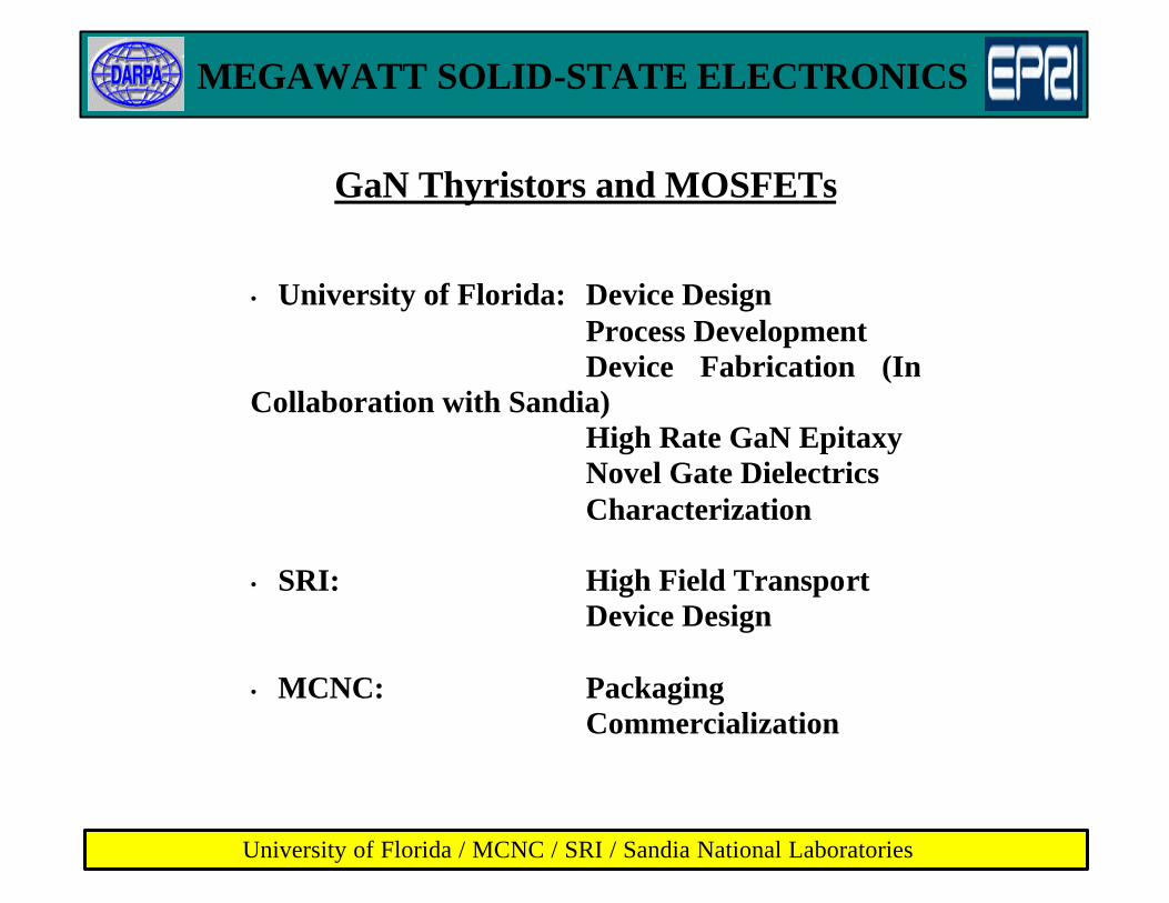
GaN Thyristors and MOSFETs
• University of Florida: Device DesignProcess DevelopmentDevice Fabrication (In
Collaboration with Sandia)High Rate GaN EpitaxyNovel Gate DielectricsCharacterization
• SRI: High Field TransportDevice Design
• MCNC: PackagingCommercialization
MEGAWATT SOLID-STATE ELECTRONICS
University of Florida / MCNC / SRI / Sandia National Laboratories
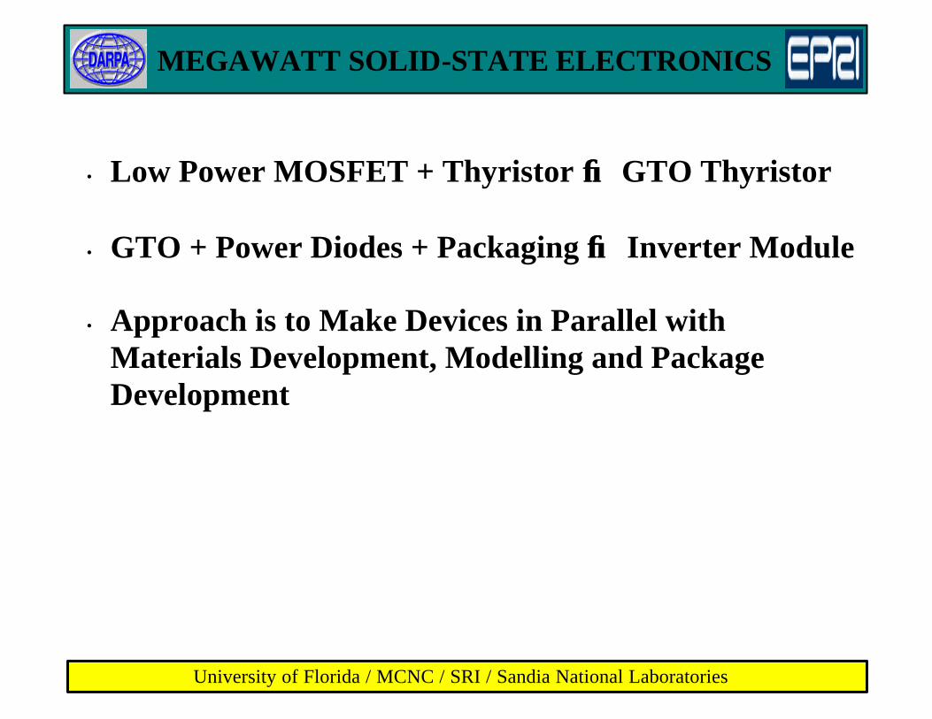
• Low Power MOSFET + Thyristor →→ GTO Thyristor
• GTO + Power Diodes + Packaging →→ Inverter Module
• Approach is to Make Devices in Parallel withMaterials Development, Modelling and PackageDevelopment
MEGAWATT SOLID-STATE ELECTRONICS
University of Florida / MCNC / SRI / Sandia National Laboratories
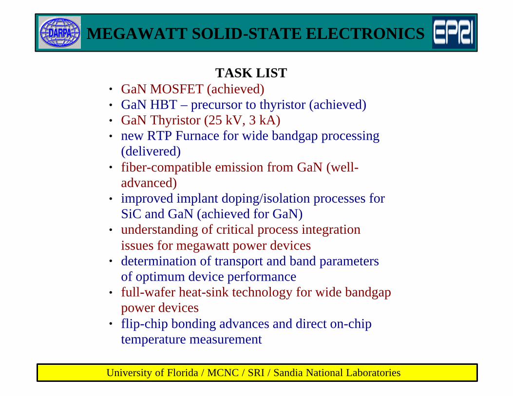
TASK LIST• GaN MOSFET (achieved)• GaN HBT – precursor to thyristor (achieved)• GaN Thyristor (25 kV, 3 kA)• new RTP Furnace for wide bandgap processing
(delivered)• fiber-compatible emission from GaN (well-
advanced)• improved implant doping/isolation processes for
SiC and GaN (achieved for GaN)• understanding of critical process integration
issues for megawatt power devices• determination of transport and band parameters
of optimum device performance• full-wafer heat-sink technology for wide bandgap
power devices• flip-chip bonding advances and direct on-chip
temperature measurement
MEGAWATT SOLID-STATE ELECTRONICS
University of Florida / MCNC / SRI / Sandia National Laboratories
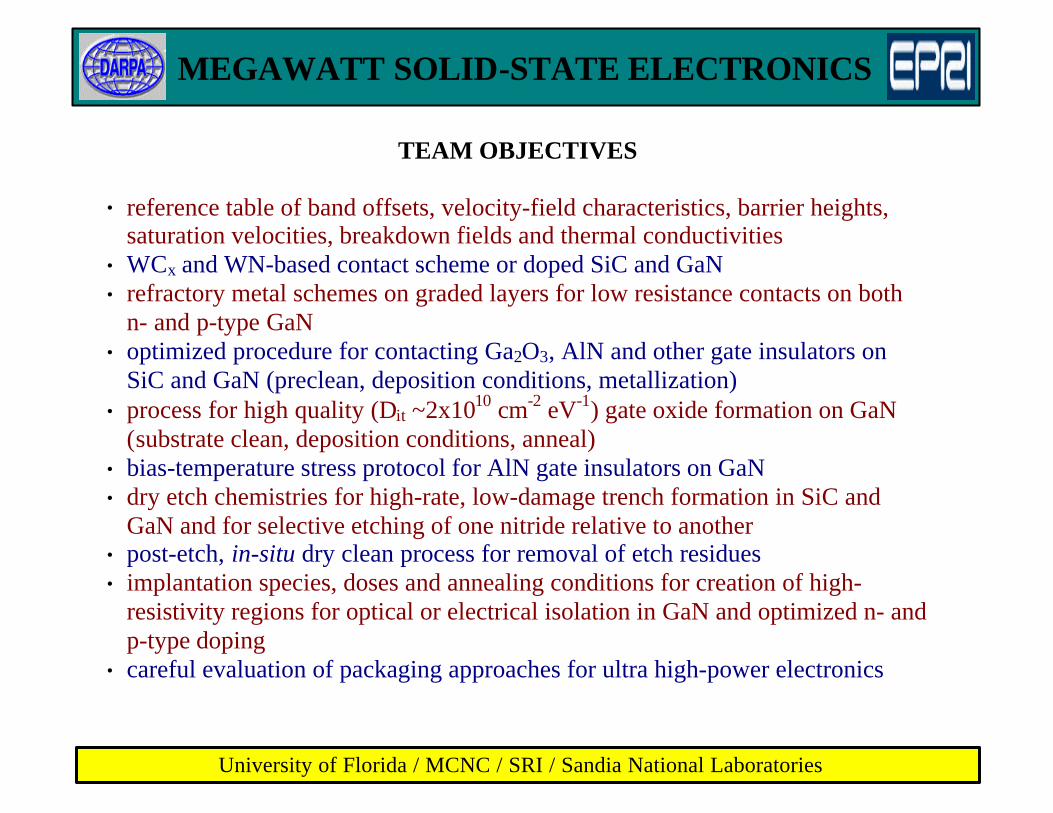
TEAM OBJECTIVES
• reference table of band offsets, velocity-field characteristics, barrier heights,saturation velocities, breakdown fields and thermal conductivities
• WCx and WN-based contact scheme or doped SiC and GaN• refractory metal schemes on graded layers for low resistance contacts on both
n- and p-type GaN• optimized procedure for contacting Ga2O3, AlN and other gate insulators on
SiC and GaN (preclean, deposition conditions, metallization)• process for high quality (Dit⋅~2x1010 cm-2 eV-1) gate oxide formation on GaN
(substrate clean, deposition conditions, anneal)• bias-temperature stress protocol for AlN gate insulators on GaN• dry etch chemistries for high-rate, low-damage trench formation in SiC and
GaN and for selective etching of one nitride relative to another• post-etch, in-situ dry clean process for removal of etch residues• implantation species, doses and annealing conditions for creation of high-
resistivity regions for optical or electrical isolation in GaN and optimized n- andp-type doping
• careful evaluation of packaging approaches for ultra high-power electronics
MEGAWATT SOLID-STATE ELECTRONICS
University of Florida / MCNC / SRI / Sandia National Laboratories
Highlights
• GaN/AlGaN HBT (precursor to thyristor)- operates at 300oC, ∃∃ = 10
• Further characterization of GaN MOSFET- operates at 400oC
• Velocity-Field characteristics for GaN
• Packaging approaches for megawatt electronics
MEGAWATT SOLID-STATE ELECTRONICS
University of Florida / MCNC / SRI / Sandia National Laboratories
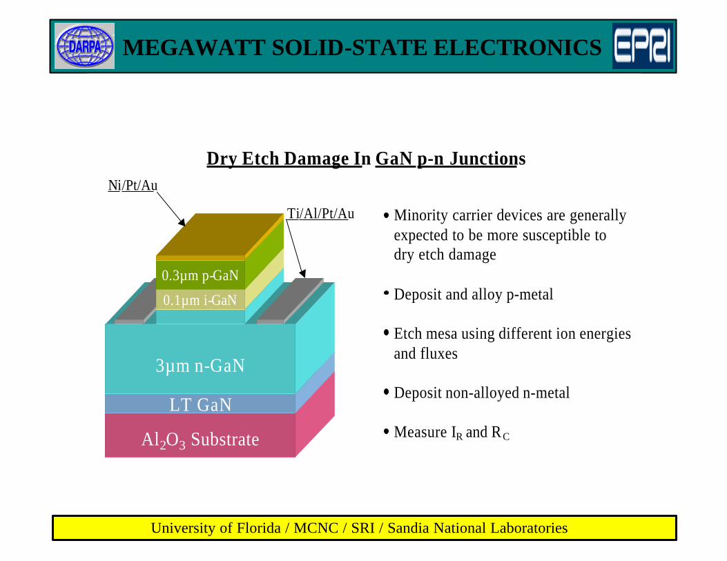
0.1µm i-GaN
0.3µm p-GaN
Al2O3 Substrate
LT GaN
3µm n-GaN
Ni/Pt/Au
Ti/Al/Pt/Au
Dry Etch Damage In GaN p-n Junctions
Minority carrier devices are generallyexpected to be more susceptible todry etch damage
Deposit and alloy p-metal
Etch mesa using different ion energiesand fluxes
Deposit non-alloyed n-metal
Measure IR and RC
MEGAWATT SOLID-STATE ELECTRONICS
University of Florida / MCNC / SRI / Sandia National Laboratories
MEGAWATT SOLID-STATE ELECTRONICS
University of Florida / MCNC / SRI / Sandia National Laboratories
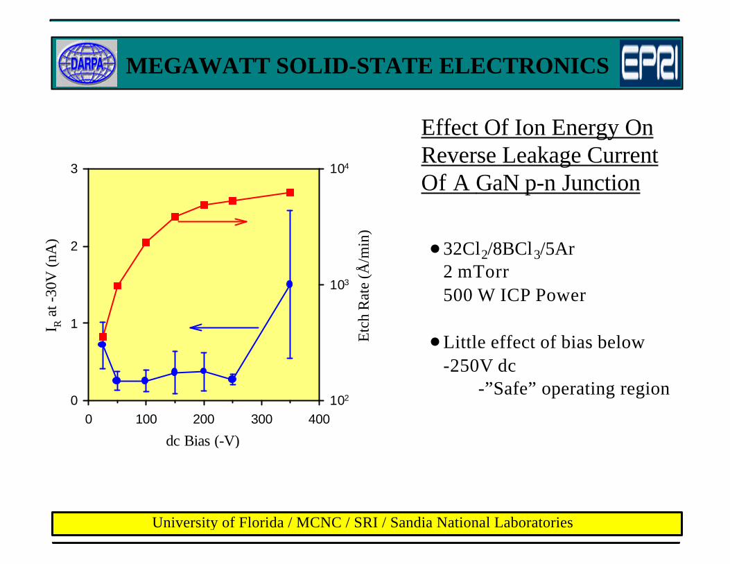
Effect Of Ion Energy OnReverse Leakage CurrentOf A GaN p-n Junction
32Cl2/8BCl3/5Ar2 mTorr500 W ICP Power
Little effect of bias below-250V dc -”Safe” operating region
dc Bias (-V)
0 100 200 300 400
I R a
t -30
V (
nA)
0
1
2
3
Etc
h R
ate
(Å/m
in)
102
103
104
MEGAWATT SOLID-STATE ELECTRONICS
University of Florida / MCNC / SRI / Sandia National Laboratories
MEGAWATT SOLID-STATE ELECTRONICS
University of Florida / MCNC / SRI / Sandia National Laboratories
ICP Power (W)
0 400 800 1200
I R a
t -3
0V (
nA)
10-1
100
101
102
103
Etc
h R
ate
(Å/m
in)
1000
2000
3000
4000
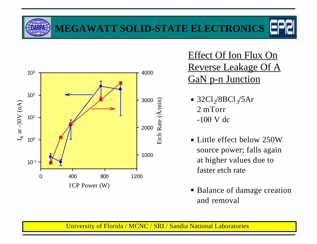
Effect Of Ion Flux OnReverse Leakage Of AGaN p-n Junction
32Cl2/8BCl 3/5Ar2 mTorr-100 V dc
Little effect below 250Wsource power; falls againat higher values due tofaster etch rate
Balance of damage creationand removal
MEGAWATT SOLID-STATE ELECTRONICS
University of Florida / MCNC / SRI / Sandia National Laboratories
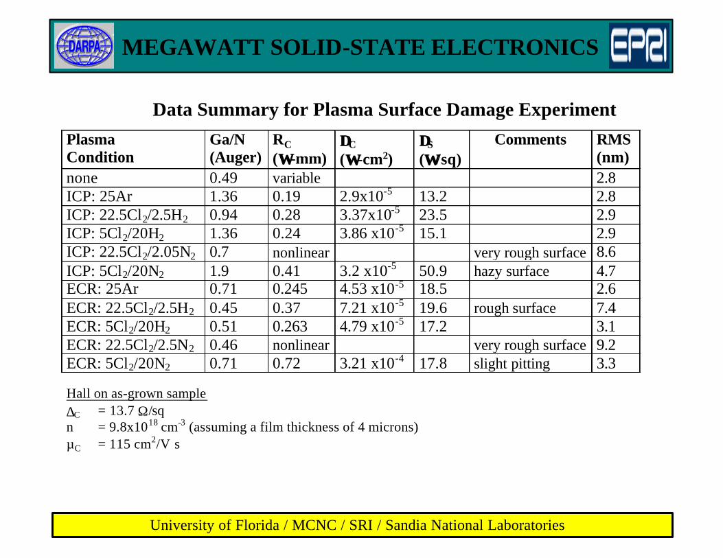
Data Summary for Plasma Surface Damage Experiment
PlasmaCondition
Ga/N(Auger)
RC
(ΩΩ-mm)∆∆C
(ΩΩ-cm2)∆∆S
(ΩΩ/sq)Comments RMS
(nm)none 0.49 variable 2.8ICP: 25Ar 1.36 0.19 2.9x10⁻⁵ 13.2 2.8ICP: 22.5Cl2/2.5H2 0.94 0.28 3.37x10⁻⁵ 23.5 2.9ICP: 5Cl2/20H2 1.36 0.24 3.86 x10⁻⁵ 15.1 2.9ICP: 22.5Cl2/2.05N2 0.7 nonlinear very rough surface 8.6ICP: 5Cl2/20N2 1.9 0.41 3.2 x10⁻⁵ 50.9 hazy surface 4.7ECR: 25Ar 0.71 0.245 4.53 x10⁻⁵ 18.5 2.6ECR: 22.5Cl2/2.5H2 0.45 0.37 7.21 x10⁻⁵ 19.6 rough surface 7.4ECR: 5Cl2/20H2 0.51 0.263 4.79 x10⁻⁵ 17.2 3.1ECR: 22.5Cl2/2.5N2 0.46 nonlinear very rough surface 9.2ECR: 5Cl2/20N2 0.71 0.72 3.21 x10⁻⁴ 17.8 slight pitting 3.3
Hall on as-grown sample∆C = 13.7 Ω/sqn = 9.8x1018 cm-3 (assuming a film thickness of 4 microns)µC = 115 cm2/V s
MEGAWATT SOLID-STATE ELECTRONICS
University of Florida / MCNC / SRI / Sandia National Laboratories
MEGAWATT SOLID-STATE ELECTRONICS
University of Florida / MCNC / SRI / Sandia National Laboratories
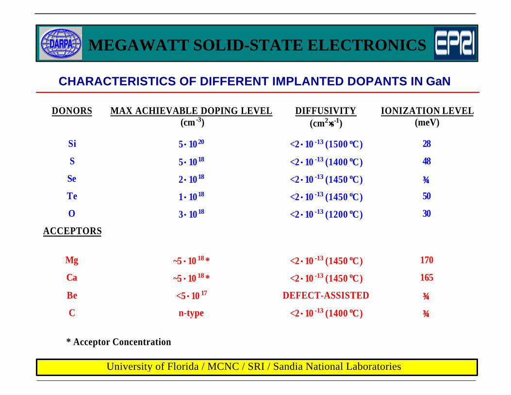
CHARACTERISTICS OF DIFFERENT IMPLANTED DOPANTS IN GaN
DONORS MAX ACHIEVABLE DOPING LEVEL (cm -3)
DIFFUSIVITY(cm2⋅⋅s-1)
IONIZATION LEVEL(meV)
Si 5××1020 <2 ××10 -13 (1500 oC) 28
S 5××1018 <2 ××10 -13 (1400 oC) 48
Se 2××1018 <2 ××10 -13 (1450 oC)
Te 1××1018 <2 ××10 -13 (1450 oC) 50
O 3××1018 <2 ××10 -13 (1200 oC) 30
ACCEPTORS
Mg ~5 ××10 18 * <2 ××10 -13 (1450 oC) 170
Ca ~5 ××10 18 * <2 ××10 -13 (1450 oC) 165
Be <5 ××10 17 DEFECT-ASSISTED
C n-type <2 ××10 -13 (1400 oC)
* Acceptor Concentration
MEGAWATT SOLID-STATE ELECTRONICS
University of Florida / MCNC / SRI / Sandia National Laboratories
MEGAWATT SOLID-STATE ELECTRONICS
University of Florida / MCNC / SRI / Sandia National Laboratories
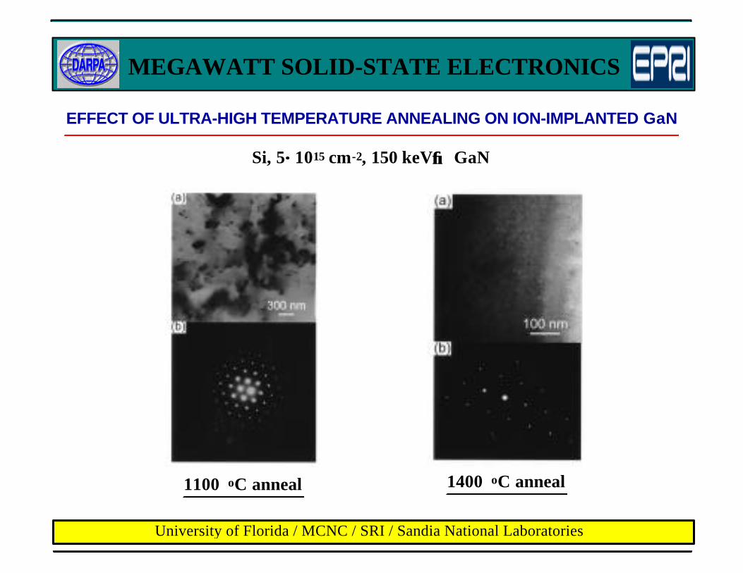
EFFECT OF ULTRA-HIGH TEMPERATURE ANNEALING ON ION-IMPLANTED GaN
Si, 5××1015 cm-2, 150 keV→→ GaN
1100 oC anneal 1400 oC anneal
MEGAWATT SOLID-STATE ELECTRONICS
University of Florida / MCNC / SRI / Sandia National Laboratories
Summary
• Fabricated GaN/AlGaN Heterojunction Bipolar Transistor- Gain of 10 at 300oC- Performance limited by base resistance
• GaN MOSFET- Further development of GdOX, AlN
• High temperature stable WSix Ohmic contacts
• Dry etch damage study
• Velocity-Field characteristics in hexagonal GaN
• Packaging strategies
MEGAWATT SOLID-STATE ELECTRONICS
University of Florida / MCNC / SRI / Sandia National Laboratories
Motivation
• High breakdown voltage and high temperature device
• Develop lower ohmic contact resistivity, thermal
stability, surface morphology, and edge definition
• Gate Recess Process
• Schottky gate vs. MOS gate - complementary circuits,
low power consumption, and single supply voltage
MEGAWATT SOLID-STATE ELECTRONICS
University of Florida / MCNC / SRI / Sandia National Laboratories
• The composite metal layers for the n-type GaN -Au/Ti/WSi/Ti/GaN (60/25/50/40nm)-Au/Ti/WSi/Ti-Al/GaN (60/25/50/10-30nm)
• The composite metal layers for the p-type GaN-Au/Ti/WSi/Pd/GaN (60/25/50/30nm)-Au/Ti/WSi/Ni/GaN (60/25/50/30nm)
• Au, Ti, Al, Pd, Ni deposited by e-beam deposition
• WSi sputtered from composite target with Arplasma
Experimental for Ohmic Contacts
MEGAWATT SOLID-STATE ELECTRONICS
University of Florida / MCNC / SRI / Sandia National Laboratories
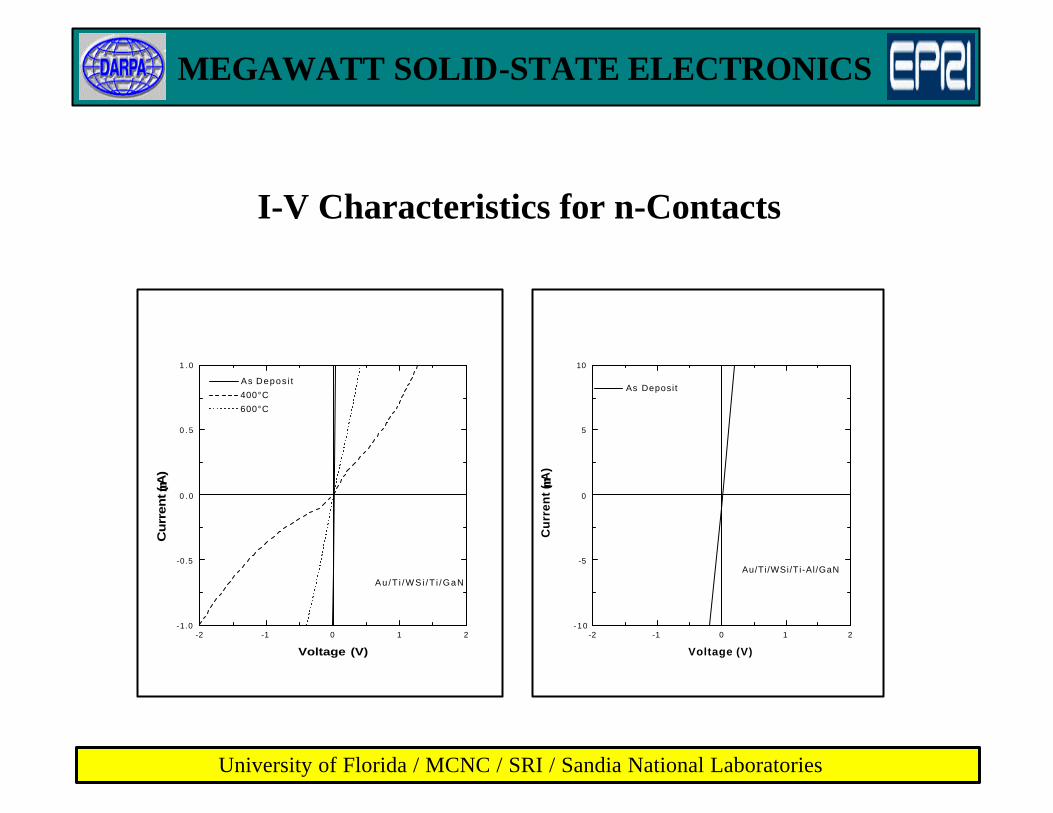
-2 -1 0 1 2- 1 0
-5
0
5
10
Au/Ti/WSi/Ti-Al/GaN
As Deposi t
Cu
rren
t ( µµ
A)
Voltage (V)
-2 -1 0 1 2-1.0
-0.5
0 . 0
0 . 5
1 . 0
Au/T i /WS i /T i /GaN
As Depos i t
400°C
600°C
Cu
rren
t ( µµA
)
Voltage (V)
I-V Characteristics for n-Contacts
MEGAWATT SOLID-STATE ELECTRONICS
University of Florida / MCNC / SRI / Sandia National Laboratories
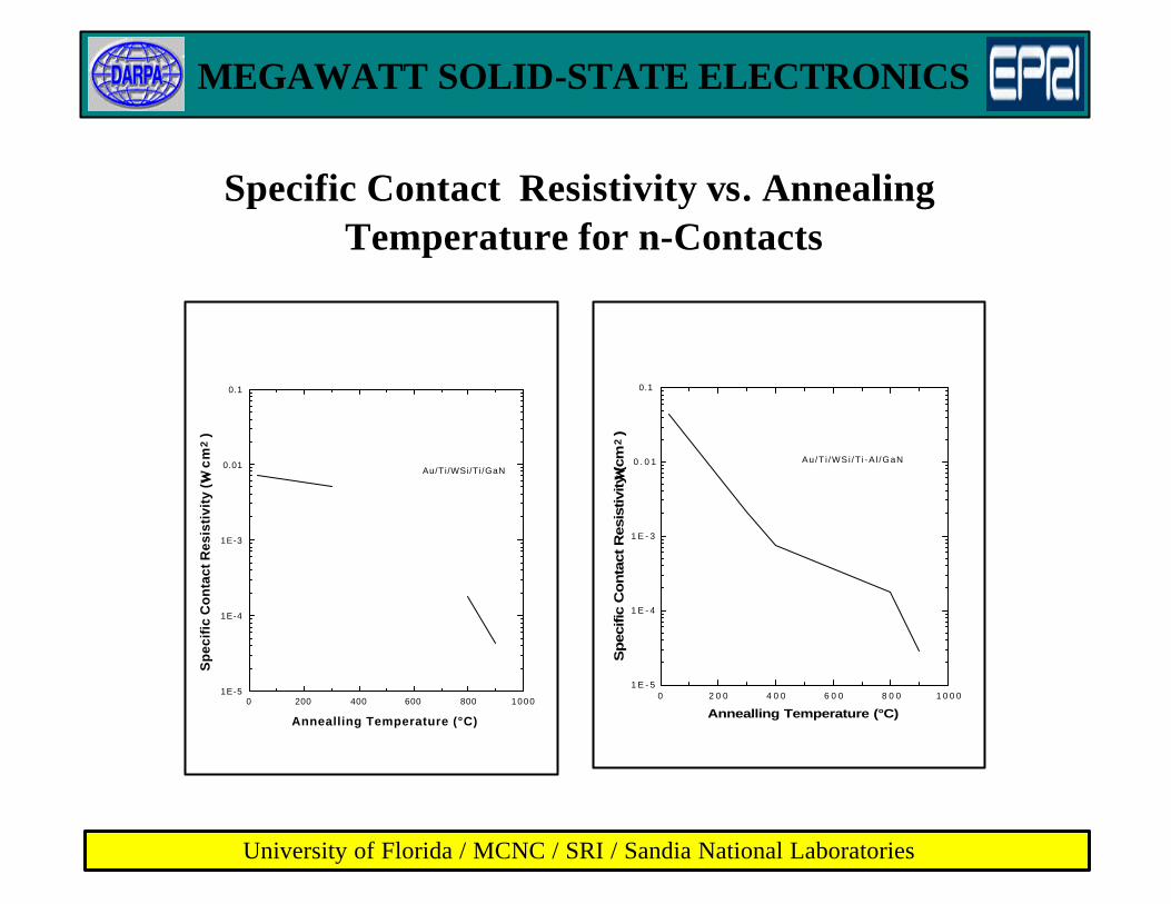
0 2 0 0 4 0 0 6 0 0 8 0 0 1 0 0 01 E - 5
1 E - 4
1 E - 3
0 . 0 1
0.1
Au/T i /WSi /T i -A l /GaN
Sp
ecific
Co
nta
ct R
esis
tivi
ty (
ΩΩ c
m 2
)
Annealling Temperature (°C)0 200 400 600 800 1000
1E-5
1E-4
1E-3
0.01
0.1
Au/Ti/WSi/Ti/GaN
Sp
ecif
ic C
on
tact
Res
isti
vity
( ΩΩ
cm
2 )
Annealling Temperature (°C)
Specific Contact Resistivity vs. Annealing Temperature for n-Contacts
MEGAWATT SOLID-STATE ELECTRONICS
University of Florida / MCNC / SRI / Sandia National Laboratories
0 50 1 0 0 1 5 0 2 0 0 2 5 0 3 0 0 3 5 0 4 0 01E-4
1E-3
0.01
0.1
Chuck Temperature (°C)
Sp
ecifi
c C
on
tact
Res
istiv
ity (
ΩΩ c
m 2
)
5 0 0
7 0 0
9 0 0
1100
1300
1500
Au/Ti/WSi/Ti-Al/n-GaN
Annealled @400°C
Sh
eet Resistan
ce ( Ω/
Ω/ sq
uare)
1 5 0 2 0 0 2 5 0 3 0 0 3 5 01 E - 4
1 E - 3
0.01
0 . 1
Chuck Temperature (°C)
Sp
ecif
ic C
on
tact
Resis
tivit
y (
ΩΩ
cm
2 )
5 0 0
7 0 0
9 0 0
1100
1300
1500
A u / T i / W S i / T i / n - G a N
A n n e a l l e d @ 4 0 0 ° C
Sh
eet R
esis
tan
ce ( ΩΩ/ sq
uare )
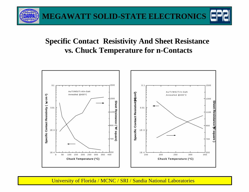
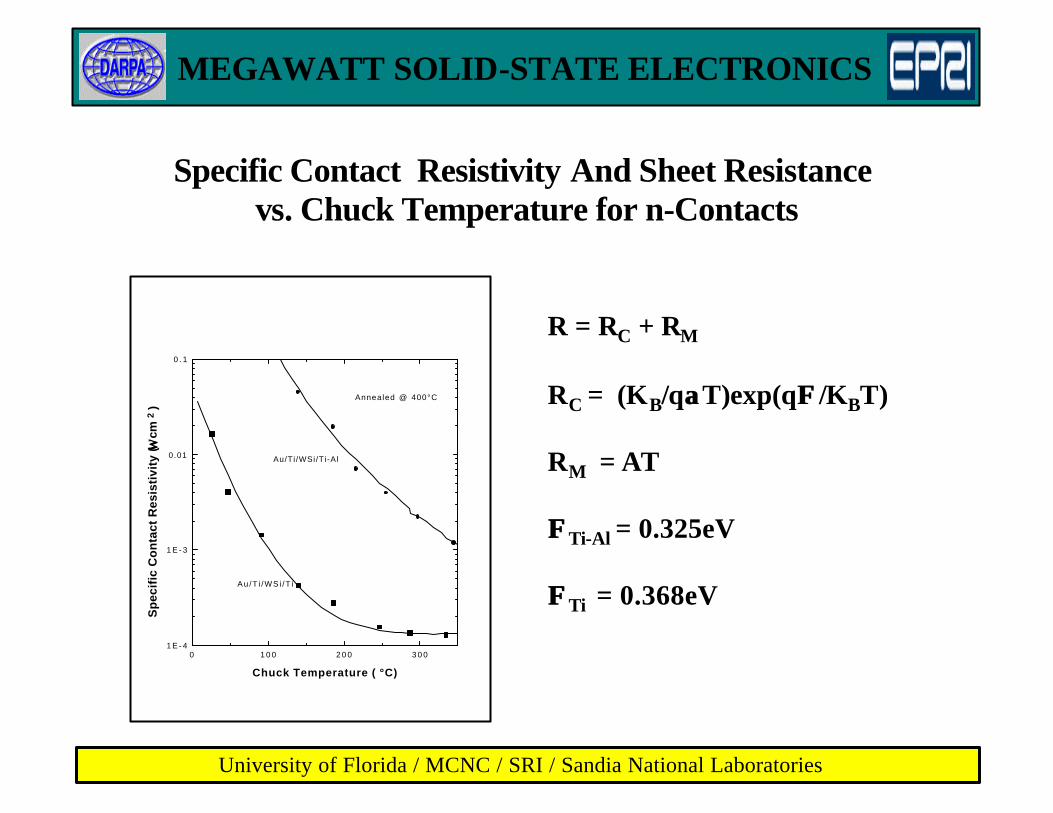
Specific Contact Resistivity And Sheet Resistance vs. Chuck Temperature for n-Contacts
MEGAWATT SOLID-STATE ELECTRONICS
University of Florida / MCNC / SRI / Sandia National Laboratories
R = RC + RM
RC = (KB/qααT)exp(qΦΦ/KBT)
RM = AT
ΦΦTi-Al = 0.325eV
ΦΦTi = 0.368eV
0 1 0 0 2 0 0 3 0 01 E - 4
1 E - 3
0.01
0 . 1
Annealed @ 400°C
Au/T i /WSi /T i
Au/Ti /WSi/Ti-Al
Sp
ecif
ic C
on
tact
Res
isti
vity
( ΩΩ c
m 2
)
Chuck Temperature ( °C)
Specific Contact Resistivity And Sheet Resistance vs. Chuck Temperature for n-Contacts
MEGAWATT SOLID-STATE ELECTRONICS
University of Florida / MCNC / SRI / Sandia National Laboratories
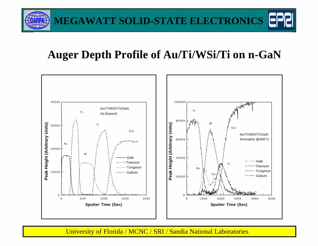
Auger Depth Profile of Au/Ti/WSi/Ti on n-GaN
0 1000 2000 3000 4000 50000
2 0 0 0 0
4 0 0 0 0
6 0 0 0 0
8 0 0 0 0
1 0 0 0 0 0
G a
T i
Au
Au
W
T i
Au/Ti/WSi/Ti/GaN
Annealed @900°C
Gold
Titanium
Tungstun
Galium
Pea
k H
eig
ht (
Arb
itra
ry U
nit
s)
Sputter Time (Sec)
0 5 0 0 1000 1500 20000
1 0 0 0 0
2 0 0 0 0
3 0 0 0 0
4 0 0 0 0
G a
T i
W
T i
Au
Au/Ti/WSi/Ti/GaN
As Deposit
Gold
Titanium
Tungstun
Galium
Pea
k H
eig
ht (
Arb
itra
ry U
nit
s)
Sputter Time (Sec)
MEGAWATT SOLID-STATE ELECTRONICS
University of Florida / MCNC / SRI / Sandia National Laboratories
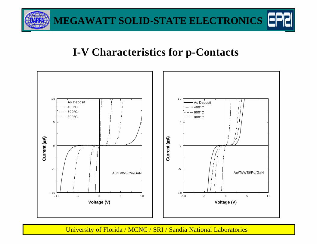
- 1 0 -5 0 5 1 0- 1 0
-5
0
5
1 0
Au/Ti/WSi/Ni/GaN
As Deposit
400°C
600°C
800°C
Cur
rent
( µµA)
Voltage (V)
- 1 0 -5 0 5 1 0- 1 0
-5
0
5
1 0
Au/Ti/WSi/Pd/GaN
As Deposit
400°C
600°C
800°C
Cur
rent
( µµA)
Voltage (V)
I-V Characteristics for p-Contacts
MEGAWATT SOLID-STATE ELECTRONICS
University of Florida / MCNC / SRI / Sandia National Laboratories
-2 -1 0 1 2-10
-5
0
5
1 0
Voltage (V)
Ni/WSi/Ni/Au
Annealled @ 400°C
As Deposit
101°C
193°C
332°C
Cu
rre
nt
( µµA
)
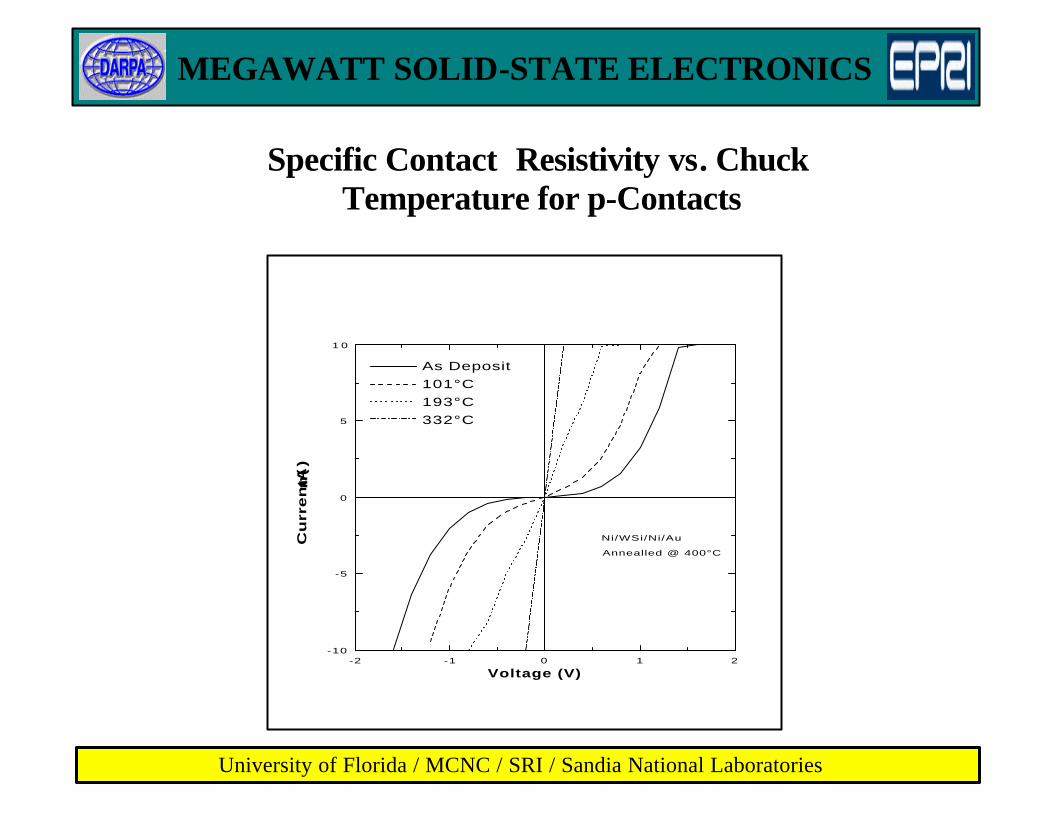
Specific Contact Resistivity vs. Chuck Temperature for p-Contacts
MEGAWATT SOLID-STATE ELECTRONICS
University of Florida / MCNC / SRI / Sandia National Laboratories
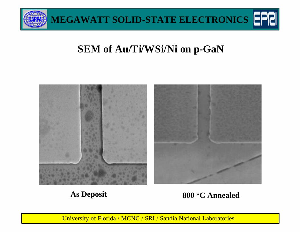
As Deposit 800 °C Annealed
SEM of Au/Ti/WSi/Ni on p-GaN
MEGAWATT SOLID-STATE ELECTRONICS
University of Florida / MCNC / SRI / Sandia National Laboratories
0 5 0 0 1000 1500 20000
5000
10000
15000
20000
25000
30000
35000
Ga
N i
W
Au
T iAu/Ti/WSi/Ni/GaN
As Deposit
Gold
Titanium
Tungstun
Nicke l
Gall ium
Pea
k H
eigh
t (A
rbitr
ary
Uni
ts)
Sputter Time (Sec)
0 1000 2000 3000 40000
15000
30000
45000
60000
75000
90000
G a
W
N i
Au
T i
Au/Ti/WSi/Ni/GaN
Annealed @900°C
Gold
Titanium
Tungstun
Nicke l
Gall ium
Pea
k H
eigh
t (A
rbitr
ary
Uni
ts)
Sputter Time (Sec)
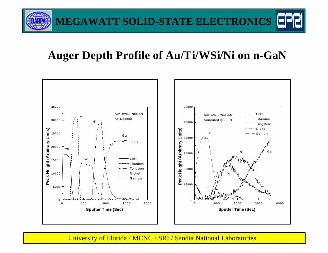
Auger Depth Profile of Au/Ti/WSi/Ni on n-GaN
MEGAWATT SOLID-STATE ELECTRONICS
University of Florida / MCNC / SRI / Sandia National Laboratories
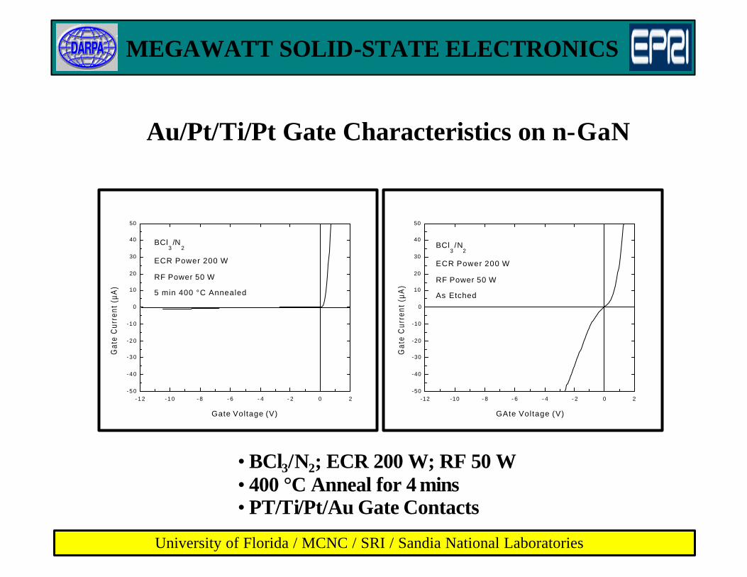
• BCl3/N2; ECR 200 W; RF 50 W• 400 °C Anneal for 4 mins• PT/Ti/Pt/Au Gate Contacts
-12 -10 - 8 - 6 - 4 - 2 0 2-50
-40
-30
-20
-10
0
10
20
30
40
50
BCl3/N
2
ECR Power 200 W
RF Power 50 W
As Etched
Ga
te C
urr
en
t (µ
A)
GAte Voltage (V)
- 1 2 - 1 0 - 8 - 6 - 4 - 2 0 2- 5 0
- 4 0
- 3 0
- 2 0
- 1 0
0
10
20
30
40
50
BCl3/N
2
ECR Power 200 W
RF Power 50 W
5 min 400 °C Annealed
Gat
e C
urre
nt (
µA
)
Gate Voltage (V)
Au/Pt/Ti/Pt Gate Characteristics on n-GaN
MEGAWATT SOLID-STATE ELECTRONICS
University of Florida / MCNC / SRI / Sandia National Laboratories
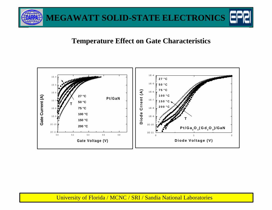
0 1 21E-11
1E-10
1 E - 9
1 E - 8
1 E - 7
1 E - 6
1 E - 5
1 E - 4
T
2 7 ° C
5 0 ° C
7 5 ° C
1 0 0 ° C
1 5 0 ° C
2 0 0 ° C
P t / G a2O
3( G d
2O
3) /GaN
Dio
de
Crr
en
t (A
)D i o d e V o l t a g e ( V )
0.0 0.2 0.4 0.6 0.81 E - 1 1
1 E - 1 0
1 E - 9
1 E - 8
1 E - 7
1 E - 6
1 E - 5
1 E - 4
T
27 °C
50 °C
75 °C
100 °C
150 °C
200 °C
P t / G a N
Gat
e C
urre
nt (A
)
Gate Voltage (V)
Temperature Effect on Gate Characteristics
MEGAWATT SOLID-STATE ELECTRONICS
University of Florida / MCNC / SRI / Sandia National Laboratories
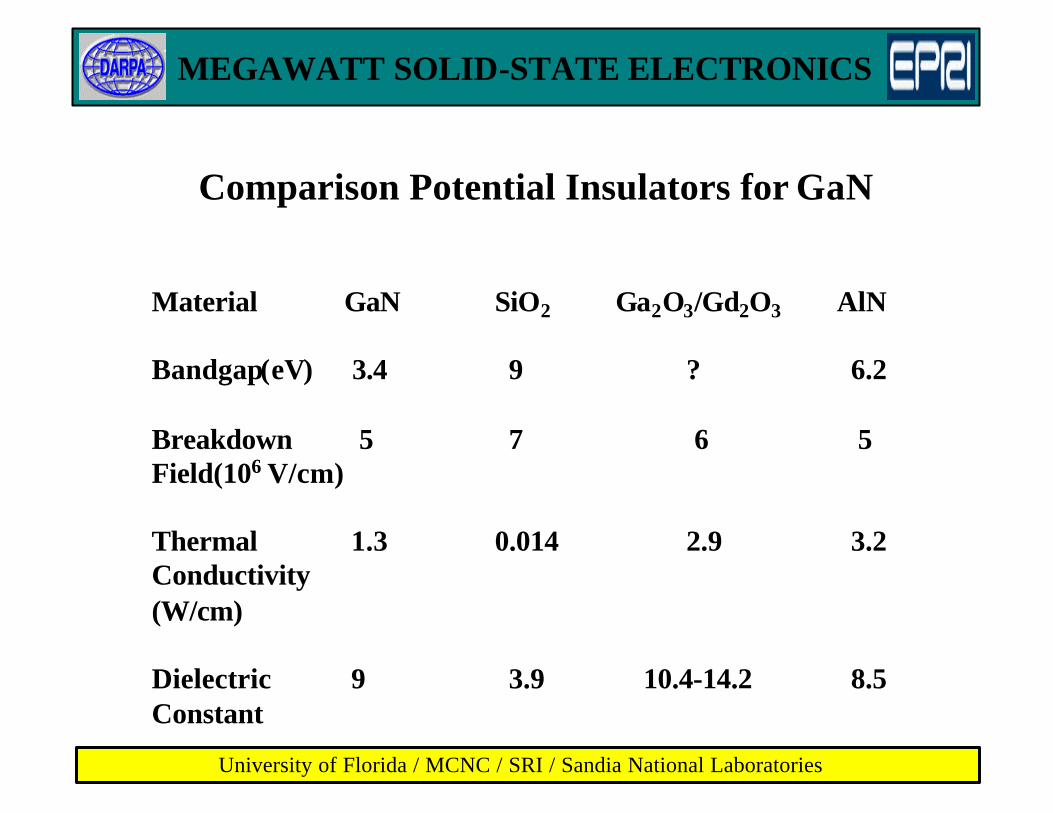
Material GaN SiO2 Ga2O3/Gd2O3 AlN
Bandgap(eV) 3.4 9 ? 6.2
Breakdown 5 7 6 5Field(106 V/cm)
Thermal 1.3 0.014 2.9 3.2Conductivity(W/cm)
Dielectric 9 3.9 10.4-14.2 8.5Constant
Comparison Potential Insulators for GaN
MEGAWATT SOLID-STATE ELECTRONICS
University of Florida / MCNC / SRI / Sandia National Laboratories
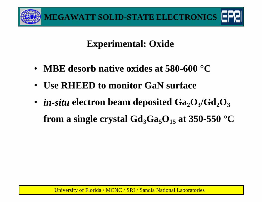
Experimental: Oxide
• MBE desorb native oxides at 580-600 °C
• Use RHEED to monitor GaN surface
• in-situ electron beam deposited Ga2O3/Gd2O3
from a single crystal Gd3Ga5O15 at 350-550 °C
MEGAWATT SOLID-STATE ELECTRONICS
University of Florida / MCNC / SRI / Sandia National Laboratories
-4 -2 0 2 4
1 E - 1 3
1 E - 1 2
1 E - 1 1
1 E - 1 0
1 E - 9
1 E - 8
1 E - 7
1 E - 6
1 E - 5
1 E - 4
1 E - 3
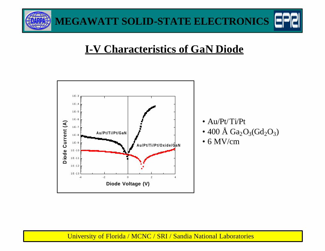
Au/Pt /T i /Pt /GaN
Au/Pt /T i /P t /Ox ide /GaN
Dio
de
Cu
rren
t (A
)
Diode Voltage (V)
I-V Characteristics of GaN Diode
• Au/Pt/Ti/Pt• 400 Å Ga2O3(Gd2O3)• 6 MV/cm
MEGAWATT SOLID-STATE ELECTRONICS
University of Florida / MCNC / SRI / Sandia National Laboratories
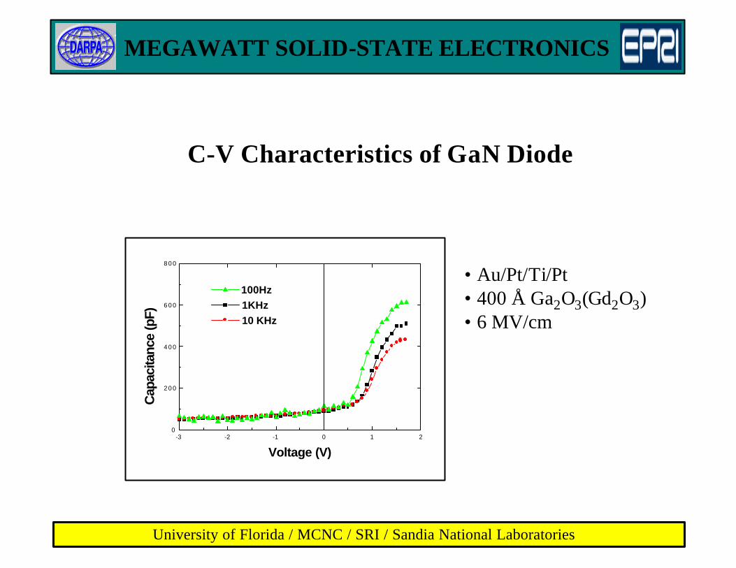
-3 -2 -1 0 1 20
2 0 0
4 0 0
6 0 0
8 0 0
100Hz 1KHz 10 KHz
Cap
acita
nce
(pF)
Voltage (V)
C-V Characteristics of GaN Diode
• Au/Pt/Ti/Pt• 400 Å Ga2O3(Gd2O3)• 6 MV/cm
MEGAWATT SOLID-STATE ELECTRONICS
University of Florida / MCNC / SRI / Sandia National Laboratories
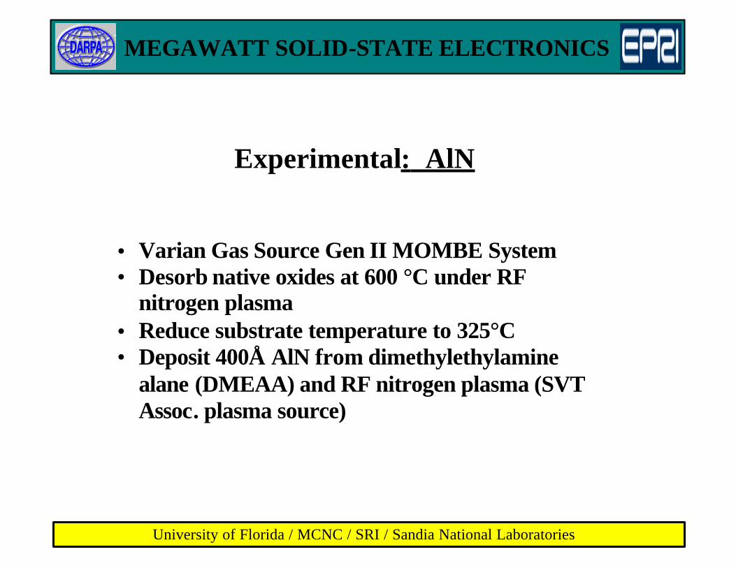
• Varian Gas Source Gen II MOMBE System• Desorb native oxides at 600 °C under RF
nitrogen plasma• Reduce substrate temperature to 325°C• Deposit 400Å AlN from dimethylethylamine
alane (DMEAA) and RF nitrogen plasma (SVTAssoc. plasma source)
Experimental: AlN
MEGAWATT SOLID-STATE ELECTRONICS
University of Florida / MCNC / SRI / Sandia National Laboratories
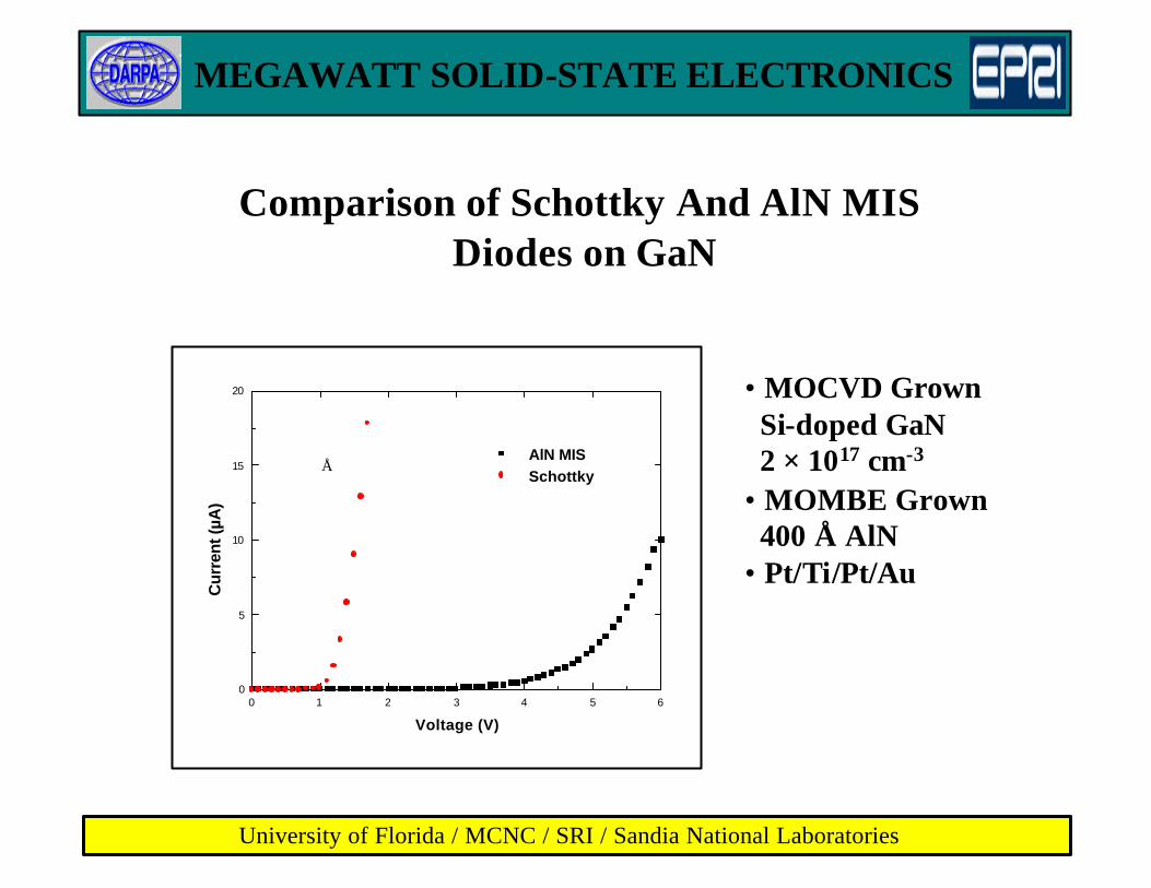
Comparison of Schottky And AlN MIS Diodes on GaN
0 1 2 3 4 5 60
5
10
15
20
AlN MIS Schottky
Cur
rent
(µA
)
Voltage (V)
• MOCVD Grown Si-doped GaN 2 × 1017 cm-3
• MOMBE Grown 400 Å AlN• Pt/Ti/Pt/Au
Å
MEGAWATT SOLID-STATE ELECTRONICS
University of Florida / MCNC / SRI / Sandia National Laboratories
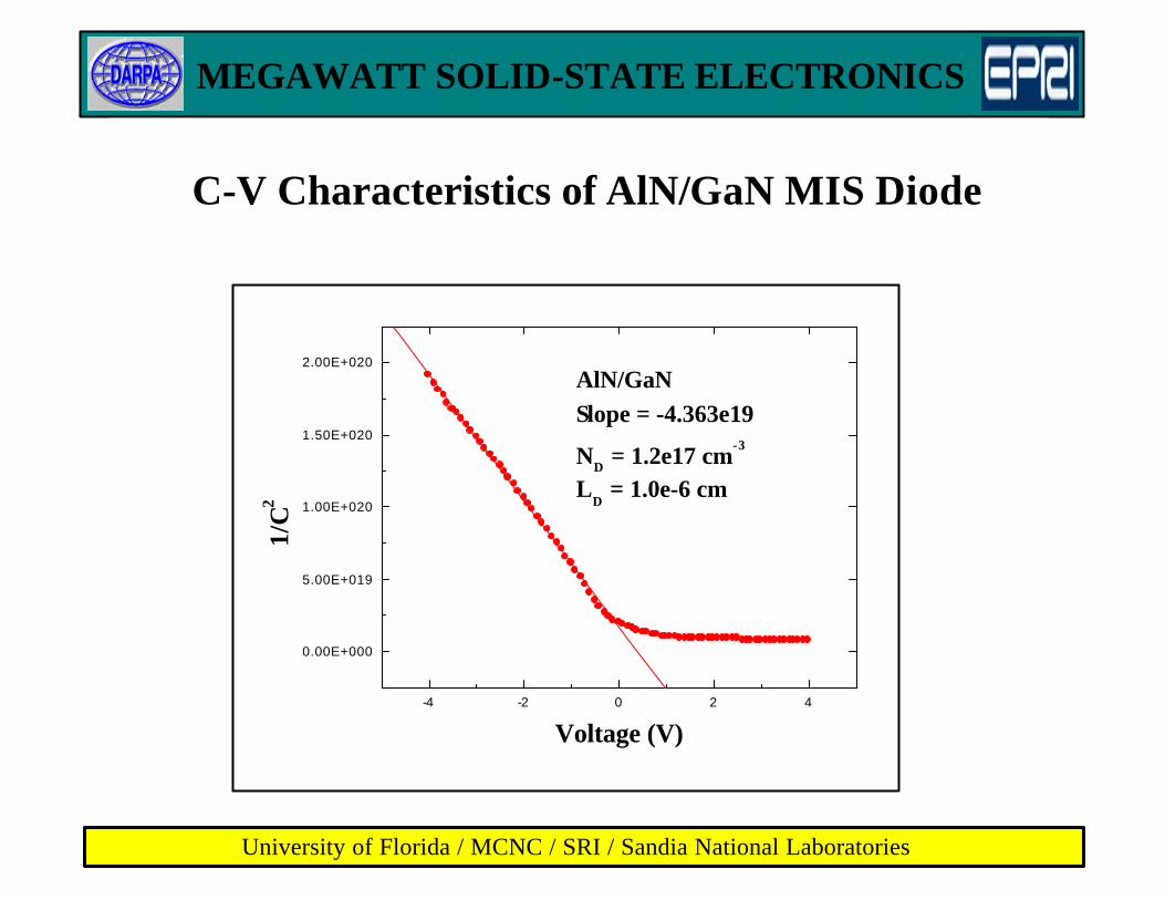
-4 -2 0 2 4
0.00E+000
5.00E+019
1.00E+020
1.50E+020
2.00E+020
AlN/GaN
Slope = -4.363e19
ND = 1.2e17 cm
-3
LD = 1.0e-6 cm
1/C
2
Voltage (V)
C-V Characteristics of AlN/GaN MIS Diode
MEGAWATT SOLID-STATE ELECTRONICS
University of Florida / MCNC / SRI / Sandia National Laboratories
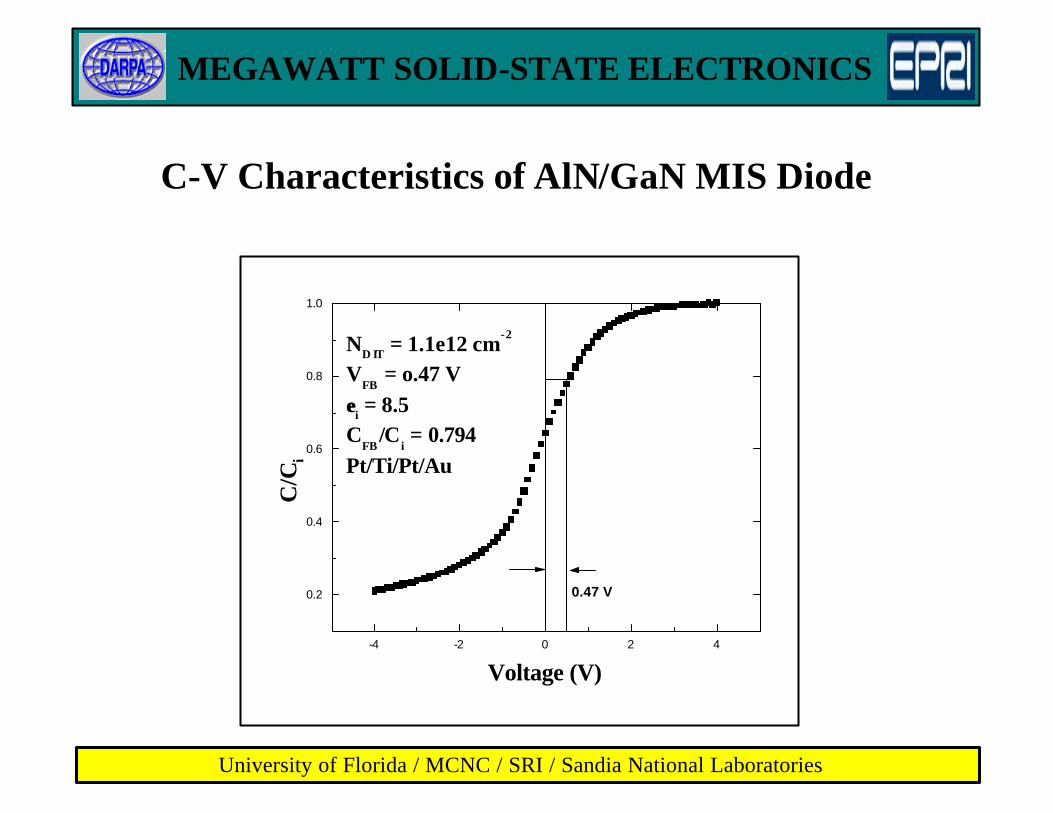
C-V Characteristics of AlN/GaN MIS Diode
-4 -2 0 2 4
0.2
0.4
0.6
0.8
1.0
0.47 V
ND IT
= 1.1e12 cm-2
VFB
= o.47 V
εεi = 8.5
CFB
/Ci = 0.794
Pt/Ti/Pt/Au
C/C
i
Voltage (V)
MEGAWATT SOLID-STATE ELECTRONICS
University of Florida / MCNC / SRI / Sandia National Laboratories
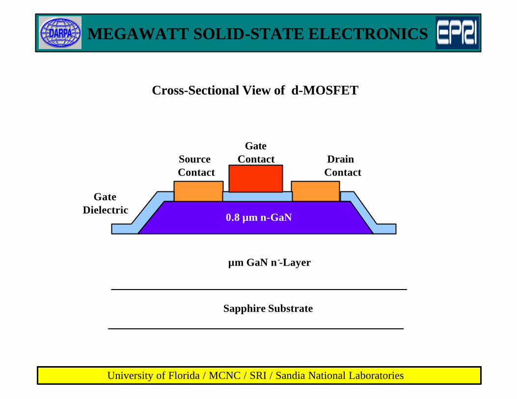
Gate Dielectric
GateContactSource
Contact
2 µm GaN n --Layer
Drain Contact
Cross-Sectional View of d-MOSFET
Sapphire Substrate
0.8 µm n-GaN
MEGAWATT SOLID-STATE ELECTRONICS
University of Florida / MCNC / SRI / Sandia National Laboratories
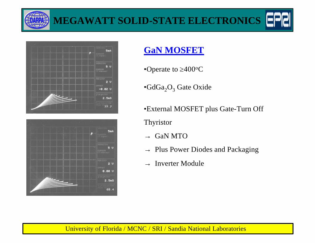
GaN MOSFET
•Operate to ≥400oC
•GdGa2O3 Gate Oxide
•External MOSFET plus Gate-Turn Off
Thyristor
→ GaN MTO
→ Plus Power Diodes and Packaging
→ Inverter Module
MEGAWATT SOLID-STATE ELECTRONICS
University of Florida / MCNC / SRI / Sandia National Laboratories
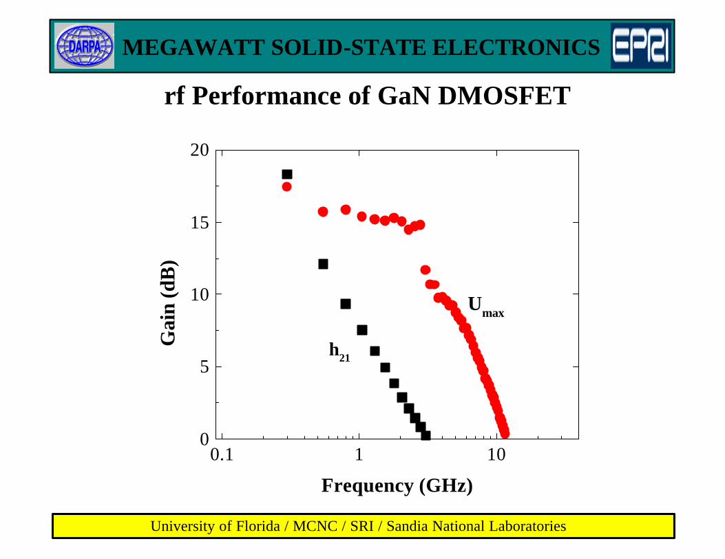
0.1 1 100
5
10
15
20
Umax
h21
Gai
n (d
B)
Frequency (GHz)
rf Performance of GaN DMOSFET
MEGAWATT SOLID-STATE ELECTRONICS
University of Florida / MCNC / SRI / Sandia National Laboratories
MEGAWATT SOLID-STATE ELECTRONICS
University of Florida / MCNC / SRI / Sandia National Laboratories
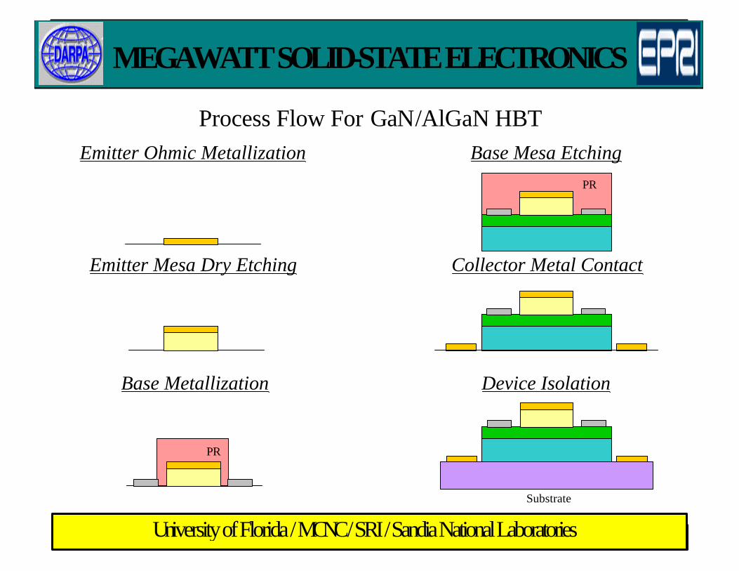
Emitter Ohmic Metallization Base Mesa Etching
Emitter Mesa Dry Etching Collector Metal Contact
Base Metallization Device Isolation
Process Flow For GaN/AlGaN HBT
Substrate
PR
PR
MEGAWATT SOLID-STATE ELECTRONICS
University of Florida / MCNC / SRI / Sandia National Laboratories
MEGAWATT SOLID-STATE ELECTRONICS
University of Florida / MCNC / SRI / Sandia National Laboratories
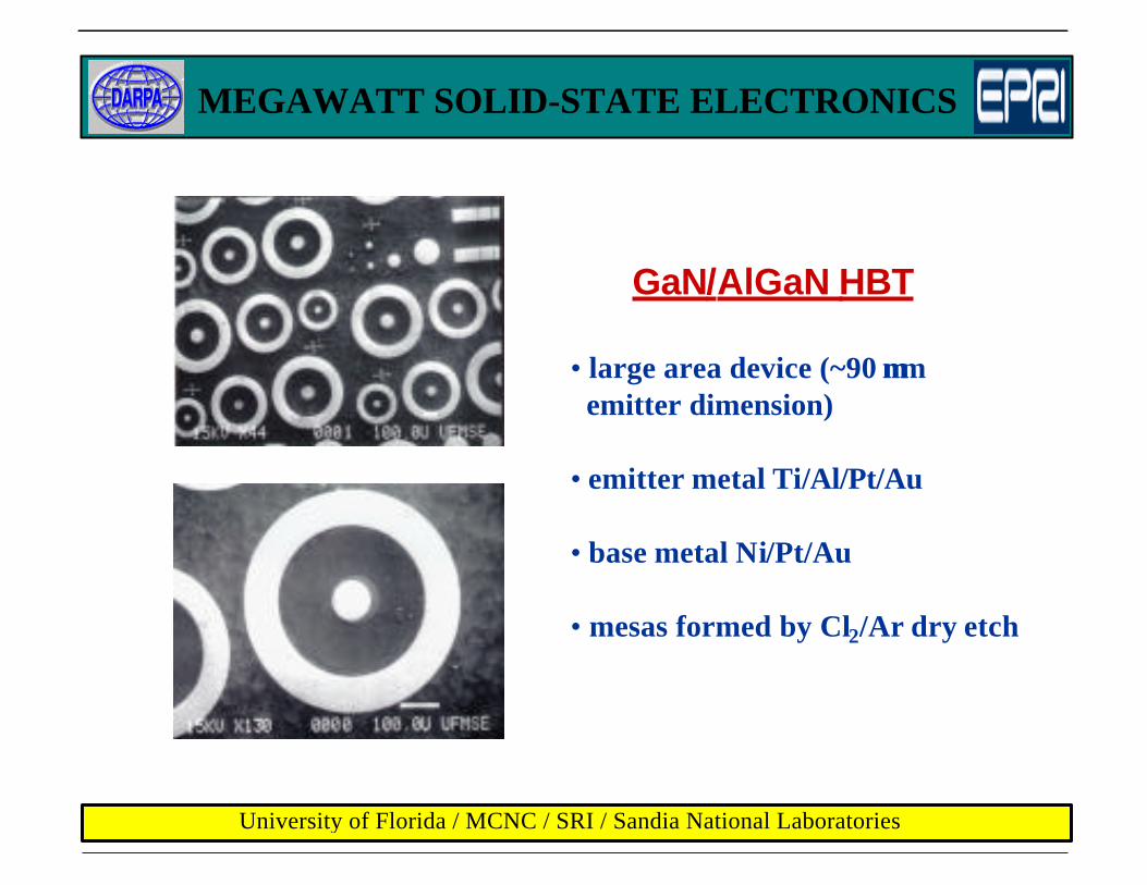
GaN/AlGaN HBT
• large area device (~90 µµm emitter dimension)
• emitter metal Ti/Al/Pt/Au
• base metal Ni/Pt/Au
• mesas formed by Cl2/Ar dry etch
MEGAWATT SOLID-STATE ELECTRONICS
University of Florida / MCNC / SRI / Sandia National Laboratories
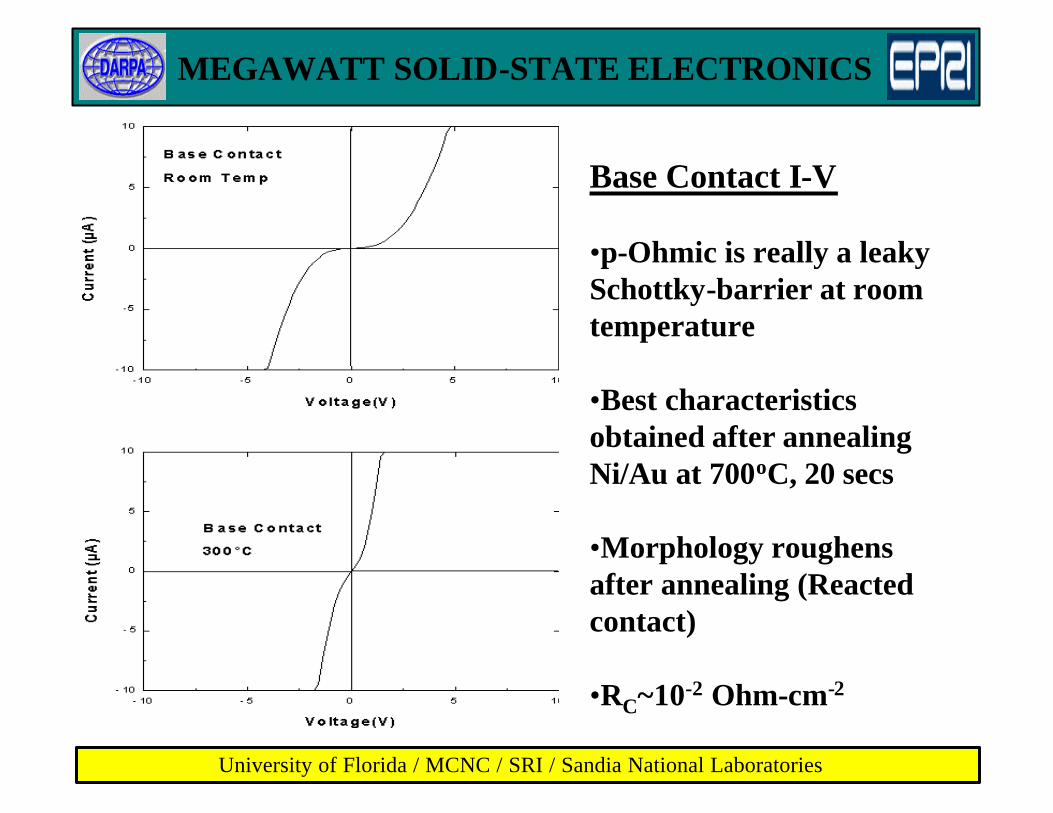
Base Contact I-V
•p-Ohmic is really a leaky Schottky-barrier at room temperature
•Best characteristics obtained after annealing Ni/Au at 700oC, 20 secs
•Morphology roughens after annealing (Reacted contact)
•RC~10-2 Ohm-cm-2
MEGAWATT SOLID-STATE ELECTRONICS
University of Florida / MCNC / SRI / Sandia National Laboratories
MEGAWATT SOLID-STATE ELECTRONICS
University of Florida / MCNC / SRI / Sandia National Laboratories
Voltage (V)
-0.4 -0.2 0.0 0.2 0.4
WSi/p-GaNC
urr
ent
(A)
W/p-GaN
Au/Ni/p-GaN
-4 x 10⁻⁶
0
4 x 10⁻⁶
1.2 x 10⁻⁵
0
-1.2 x 10⁻⁵
2 x 10⁻⁵
0
-2 x 10⁻⁵
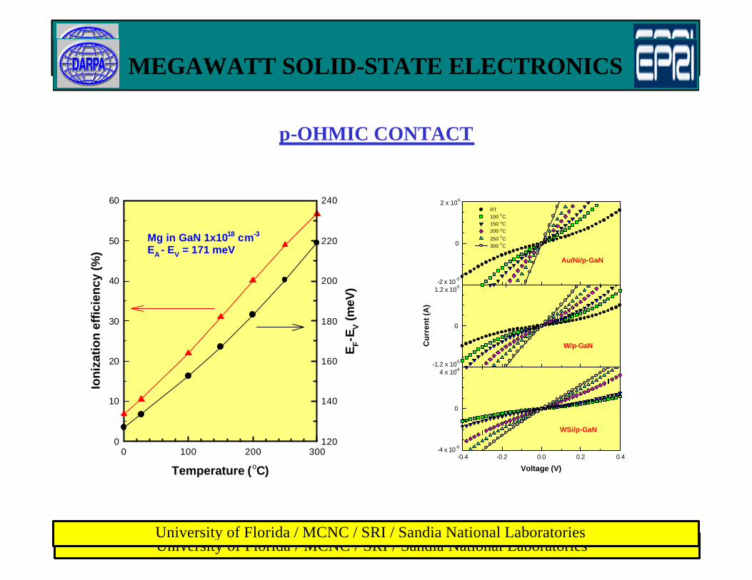
RT
100 oC
150 oC
200 oC
250 oC
300 oC
Temperature (oC)
0 100 200 300
Ion
izat
ion
eff
icie
ncy
(%)
0
10
20
30
40
50
60
EF-E
V (
meV
)
120
140
160
180
200
220
240
Mg in GaN 1x1018 cm-3
EA - EV = 171 meV
p-OHMIC CONTACT
MEGAWATT SOLID-STATE ELECTRONICS
University of Florida / MCNC / SRI / Sandia National Laboratories
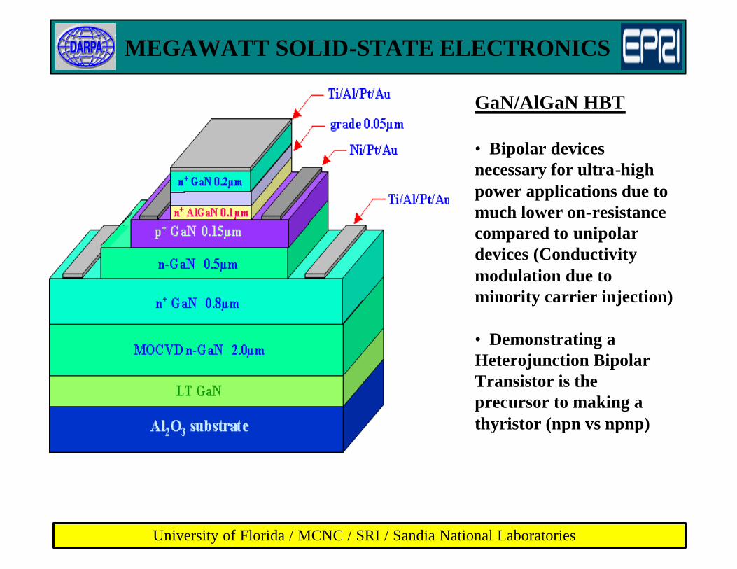
GaN/AlGaN HBT
• Bipolar devices necessary for ultra-high power applications due to much lower on-resistance compared to unipolardevices (Conductivity modulation due to minority carrier injection)
• Demonstrating a Heterojunction Bipolar Transistor is the precursor to making a thyristor (npn vs npnp)
MEGAWATT SOLID-STATE ELECTRONICS
University of Florida / MCNC / SRI / Sandia National Laboratories
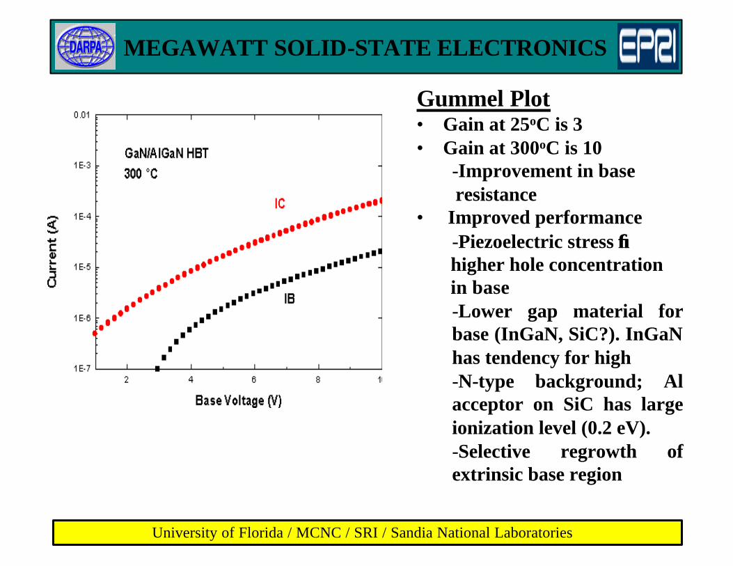
Gummel Plot• Gain at 25oC is 3• Gain at 300oC is 10
-Improvement in baseresistance
• Improved performance-Piezoelectric stress →→higher hole concentration in base-Lower gap material for base (InGaN, SiC?). InGaN has tendency for high -N-type background; Al acceptor on SiC has large ionization level (0.2 eV).-Selective regrowth of extrinsic base region
MEGAWATT SOLID-STATE ELECTRONICS
University of Florida / MCNC / SRI / Sandia National Laboratories
MEGAWATT SOLID-STATE ELECTRONICS
University of Florida / MCNC / SRI / Sandia National Laboratories
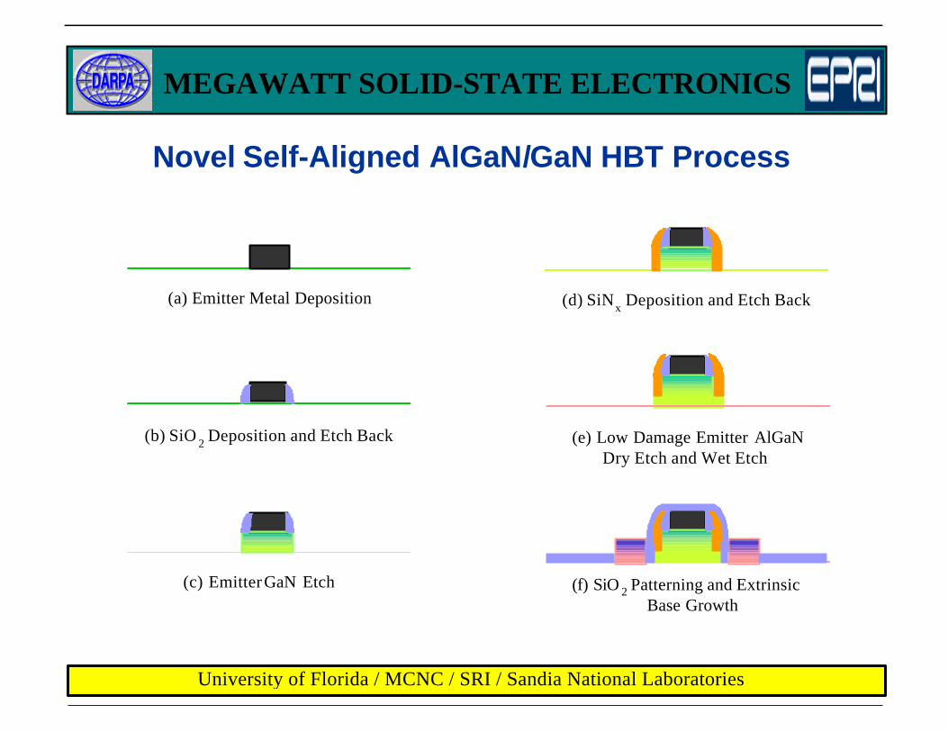
Novel Self-Aligned AlGaN/GaN HBT Process
(a) Emitter Metal Deposition
(f) SiO 2 Patterning and Extrinsic Base Growth
(b) SiO 2 Deposition and Etch Back
(c) Emitter GaN Etch
(d) SiNx Deposition and Etch Back
(e) Low Damage Emitter AlGaN Dry Etch and Wet Etch
MEGAWATT SOLID-STATE ELECTRONICS
University of Florida / MCNC / SRI / Sandia National Laboratories
MEGAWATT SOLID-STATE ELECTRONICS
University of Florida / MCNC / SRI / Sandia National Laboratories
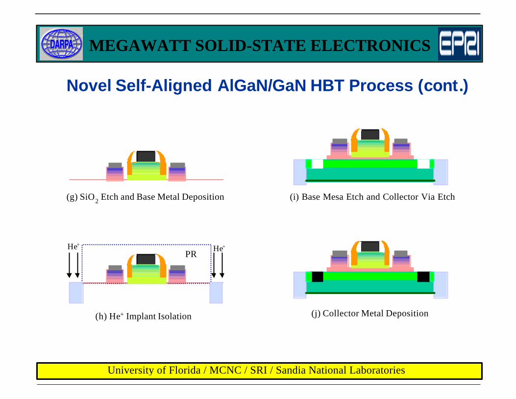
Novel Self-Aligned AlGaN/GaN HBT Process (cont.)
(g) SiO2 Etch and Base Metal Deposition
(h) He+ Implant Isolation
(i) Base Mesa Etch and Collector Via Etch
(j) Collector Metal Deposition
He+ He+
PR
MEGAWATT SOLID-STATE ELECTRONICS
University of Florida / MCNC / SRI / Sandia National Laboratories
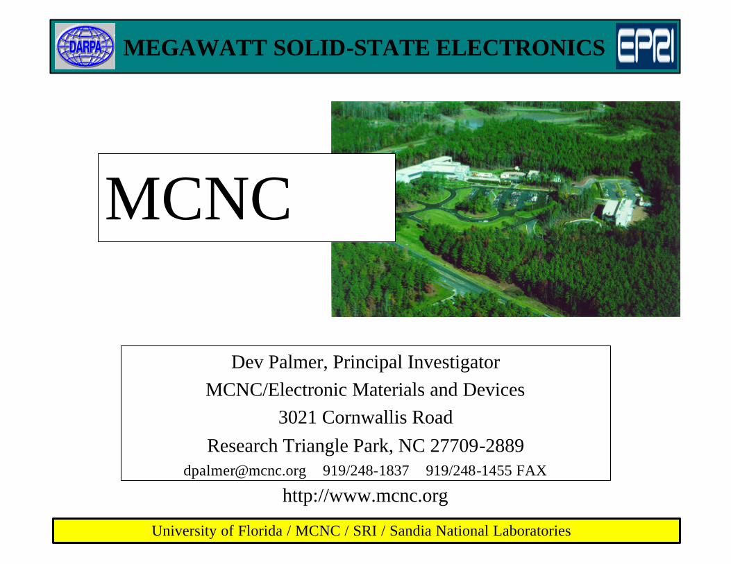
Dev Palmer, Principal Investigator
MCNC/Electronic Materials and Devices
3021 Cornwallis Road
Research Triangle Park, NC [email protected] 919/248-1837 919/248-1455 FAX
http://www.mcnc.org
MCNC
MEGAWATT SOLID-STATE ELECTRONICS
University of Florida / MCNC / SRI / Sandia National Laboratories
MCNC Information Technologies
• North Carolina Research and Education Network– Internet, Internet 2, Network Security
• North Carolina Supercomputing Center– Heterogeneous, high performance computing
environment for academic/industrial users
– Time is available on a CPU-hour basis
– Cray Research T916 parallel vector processor
MEGAWATT SOLID-STATE ELECTRONICS
University of Florida / MCNC / SRI / Sandia National Laboratories
MCNC Electronic Technologies• Electronic Materials and Devices
– AES, SIMS, XPS, and TEM composition and structure analysis
– Design and fabrication facilities
• Advanced Packaging and Interconnect– Thermal, Mechanical, and Electrical modeling
software
– Reliability test facilities
• Corporate– Marketing experience and expertise
MEGAWATT SOLID-STATE ELECTRONICS
University of Florida / MCNC / SRI / Sandia National Laboratories
MCNC Team Members• Dev Palmer - Principal Investigator
• Dorota Temple - Materials Scientist
• Richard LaBennet - Packaging Engineer
• Mark Ray - AES/SIMS Analyst
• John Lannon - XPS Analyst
• Mike Lamvik - TEM Microscopist
• Jesko von Windheim - Marketing
• Gary McGuire - Director, Electronic Materials And Devices
MEGAWATT SOLID-STATE ELECTRONICS
University of Florida / MCNC / SRI / Sandia National Laboratories
MCNC Team FocusYear 1 – Analysis of film microstructure and morphology
– Dopant depth profiling
– Market analysis
Year 2 – Materials analysis
– Test structure and device layout
– High-power package design
– Market applications analysis
Year 3 – Materials analysis
– Test structure and device fabrication
– Device packaging
– Customer development
MEGAWATT SOLID-STATE ELECTRONICS
University of Florida / MCNC / SRI / Sandia National Laboratories
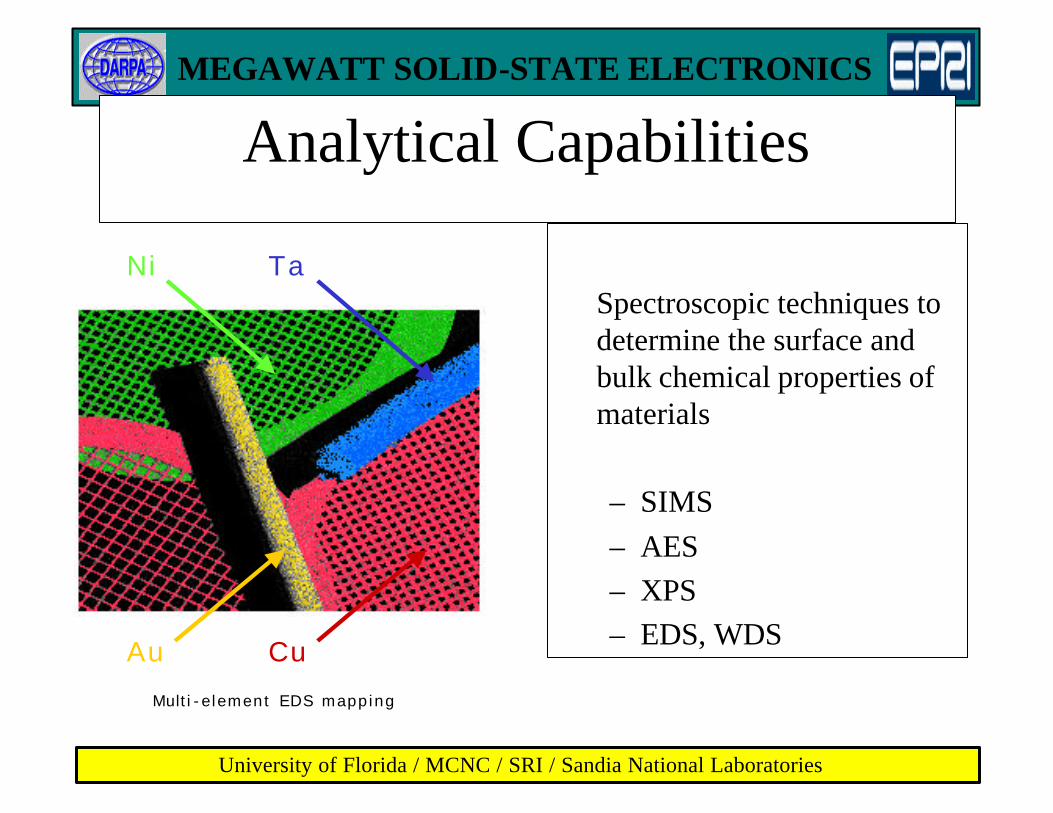
Ni Ta
Au C u
Analytical Capabilities
Spectroscopic techniques to determine the surface and bulk chemical properties of materials
– SIMS
– AES– XPS– EDS, WDS
Multi - e lement EDS mapp ing
MEGAWATT SOLID-STATE ELECTRONICS
University of Florida / MCNC / SRI / Sandia National Laboratories
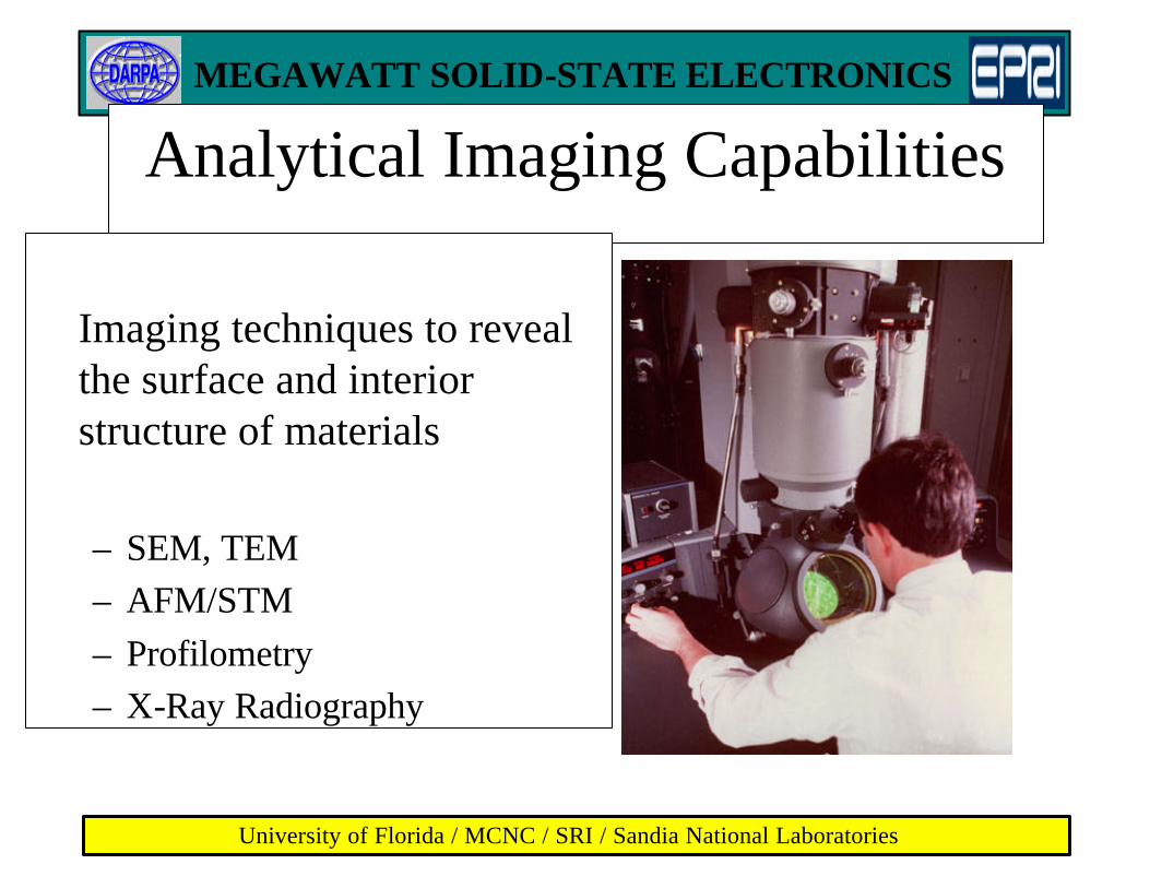
Analytical Imaging Capabilities
Imaging techniques to reveal the surface and interior structure of materials
– SEM, TEM– AFM/STM
– Profilometry– X-Ray Radiography
MEGAWATT SOLID-STATE ELECTRONICS
University of Florida / MCNC / SRI / Sandia National Laboratories
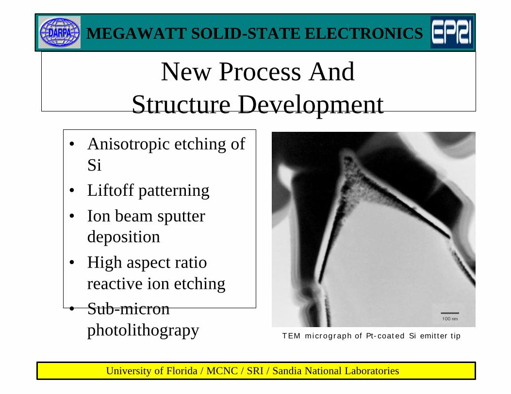
New Process AndStructure Development
• Anisotropic etching of Si
• Liftoff patterning
• Ion beam sputter deposition
• High aspect ratio reactive ion etching
• Sub-micron photolithograpy T E M micrograph of Pt- coated Si emitter tip
MEGAWATT SOLID-STATE ELECTRONICS
University of Florida / MCNC / SRI / Sandia National Laboratories
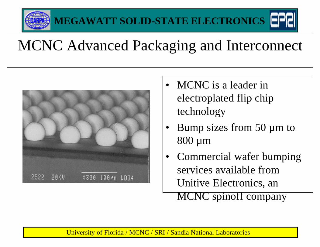
MCNC Advanced Packaging and Interconnect
• MCNC is a leader in electroplated flip chip technology
• Bump sizes from 50 µm to 800 µm
• Commercial wafer bumping services available fromUnitive Electronics, an MCNC spinoff company
MEGAWATT SOLID-STATE ELECTRONICS
University of Florida / MCNC / SRI / Sandia National Laboratories
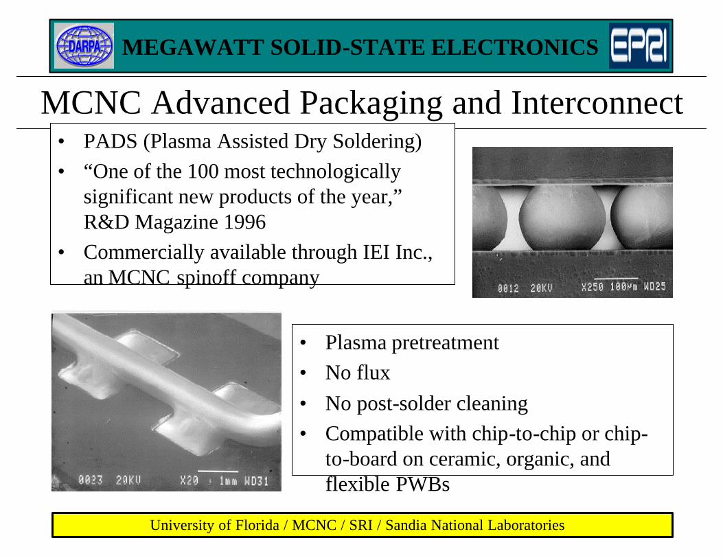
MCNC Advanced Packaging and Interconnect• PADS (Plasma Assisted Dry Soldering)• “One of the 100 most technologically
significant new products of the year,” R&D Magazine 1996
• Commercially available through IEI Inc., an MCNC spinoff company
• Plasma pretreatment• No flux
• No post-solder cleaning• Compatible with chip-to-chip or chip-
to-board on ceramic, organic, and flexible PWBs
MEGAWATT SOLID-STATE ELECTRONICS
University of Florida / MCNC / SRI / Sandia National Laboratories
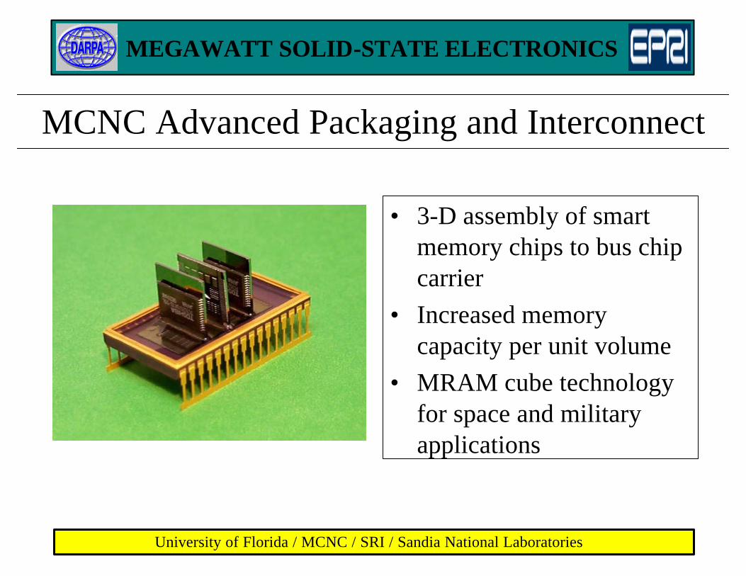
MCNC Advanced Packaging and Interconnect
• 3-D assembly of smart memory chips to bus chip carrier
• Increased memory capacity per unit volume
• MRAM cube technology for space and military applications
MEGAWATT SOLID-STATE ELECTRONICS
University of Florida / MCNC / SRI / Sandia National Laboratories
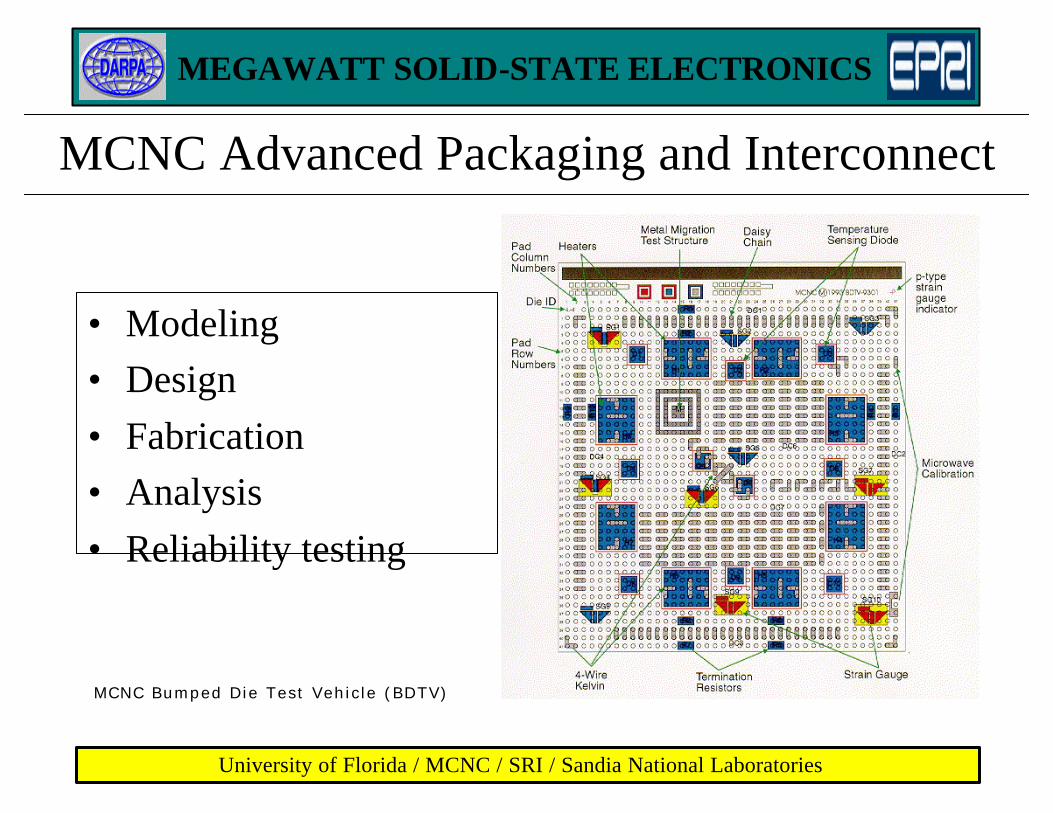
MCNC Advanced Packaging and Interconnect
• Modeling
• Design
• Fabrication
• Analysis
• Reliability testing
MCNC Bumped D i e Tes t Veh i c l e (BDTV)
MEGAWATT SOLID-STATE ELECTRONICS
University of Florida / MCNC / SRI / Sandia National Laboratories
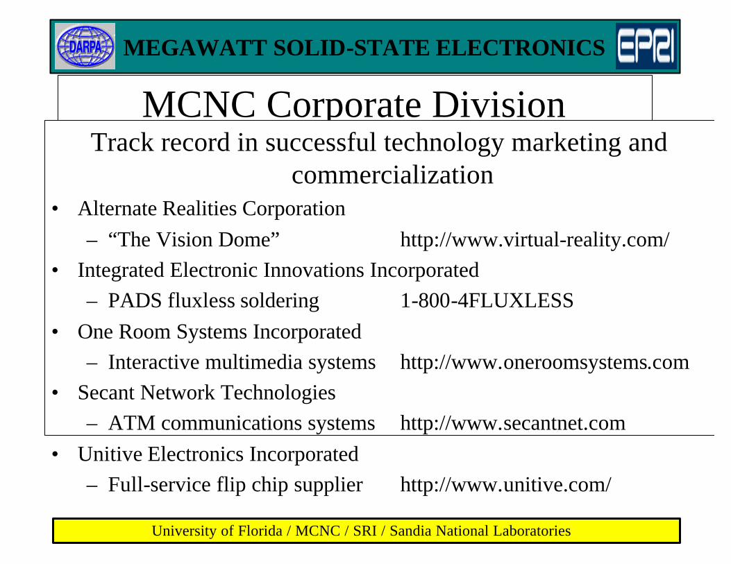
MCNC Corporate DivisionTrack record in successful technology marketing and
commercialization• Alternate Realities Corporation
– “The Vision Dome” http://www.virtual-reality.com/• Integrated Electronic Innovations Incorporated
– PADS fluxless soldering 1-800-4FLUXLESS
• One Room Systems Incorporated– Interactive multimedia systems http://www.oneroomsystems.com
• Secant Network Technologies– ATM communications systems http://www.secantnet.com
• Unitive Electronics Incorporated– Full-service flip chip supplier http://www.unitive.com/
MEGAWATT SOLID-STATE ELECTRONICS
University of Florida / MCNC / SRI / Sandia National Laboratories
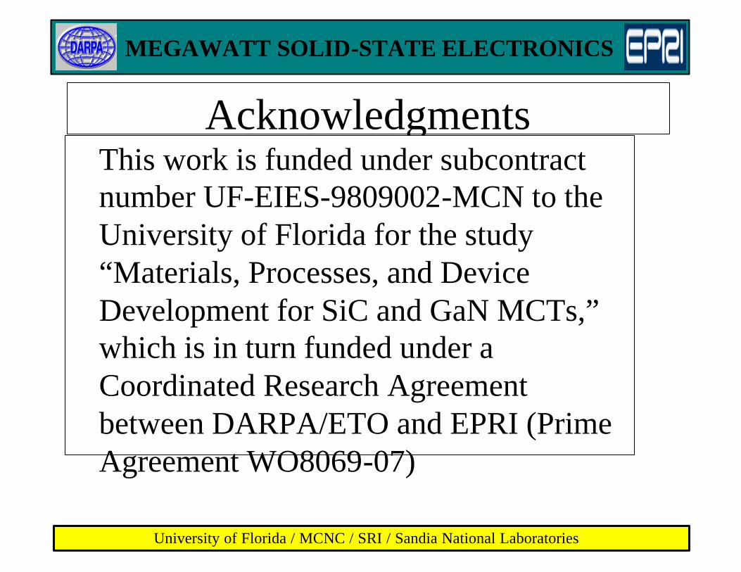
AcknowledgmentsThis work is funded under subcontract number UF-EIES-9809002-MCN to the University of Florida for the study “Materials, Processes, and Device Development for SiC and GaN MCTs,” which is in turn funded under a Coordinated Research Agreement between DARPA/ETO and EPRI (Prime Agreement WO8069-07)