ltc6803-2/ltc6803-4 - multicell battery stack...
TRANSCRIPT
LTC6803-2/LTC6803-4
1680324fa
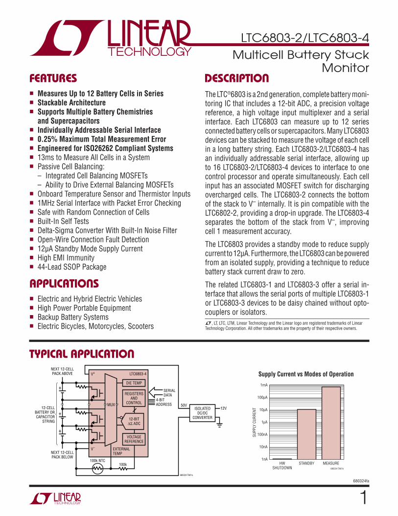
TYPICAL APPLICATION
FEATURES DESCRIPTION
Multicell Battery Stack Monitor
The LTC®6803 is a 2nd generation, complete battery moni-toring IC that includes a 12-bit ADC, a precision voltage reference, a high voltage input multiplexer and a serial interface. Each LTC6803 can measure up to 12 series connected battery cells or supercapacitors. Many LTC6803 devices can be stacked to measure the voltage of each cell in a long battery string. Each LTC6803-2/LTC6803-4 has an individually addressable serial interface, allowing up to 16 LTC6803-2/LTC6803-4 devices to interface to one control processor and operate simultaneously. Each cell input has an associated MOSFET switch for discharging overcharged cells. The LTC6803-2 connects the bottom of the stack to V– internally. It is pin compatible with the LTC6802-2, providing a drop-in upgrade. The LTC6803-4 separates the bottom of the stack from V–, improving cell 1 measurement accuracy.
The LTC6803 provides a standby mode to reduce supply current to 12µA. Furthermore, the LTC6803 can be powered from an isolated supply, providing a technique to reduce battery stack current draw to zero.
The related LTC6803-1 and LTC6803-3 offer a serial in-terface that allows the serial ports of multiple LTC6803-1 or LTC6803-3 devices to be daisy chained without opto-couplers or isolators.
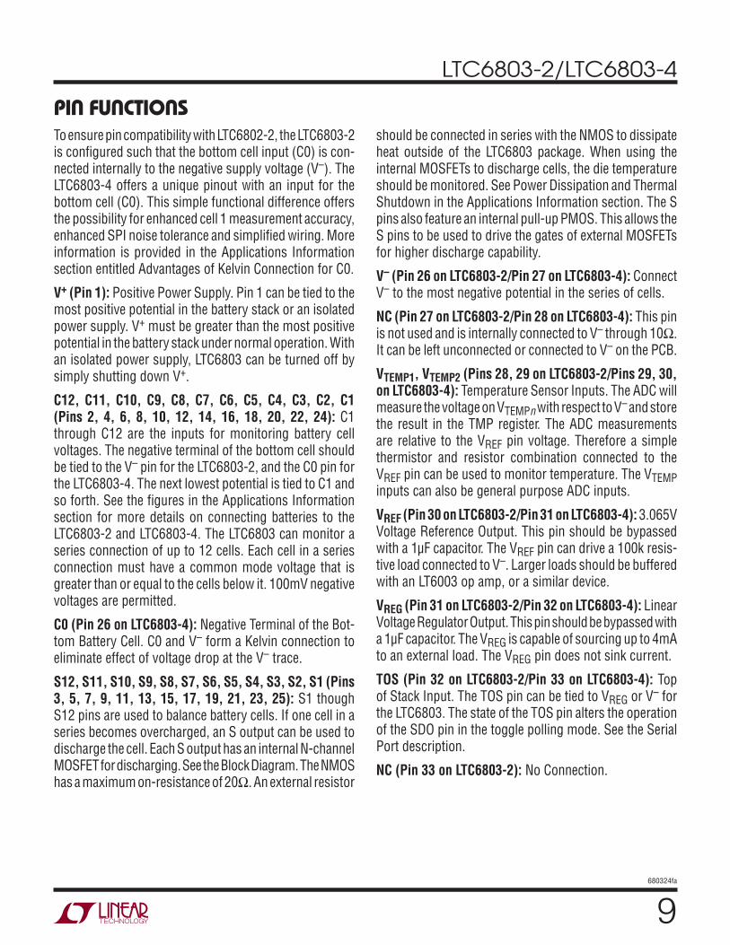
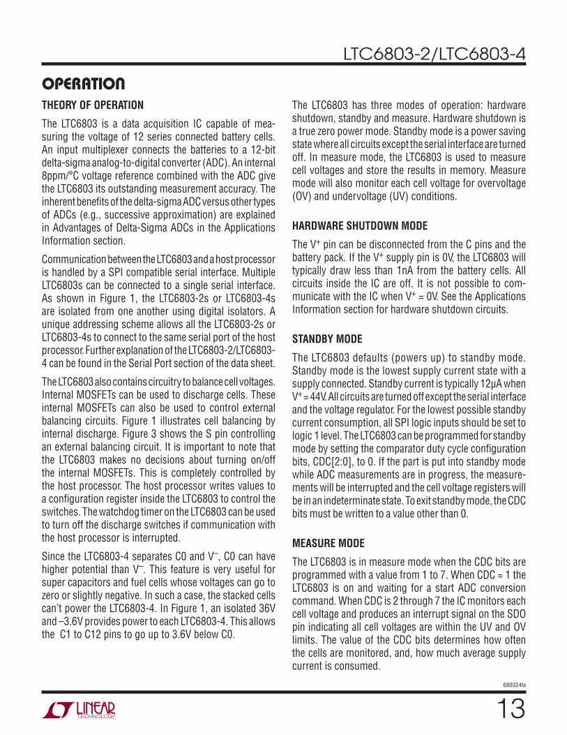
Supply Current vs Modes of Operation
APPLICATIONS
n Measures Up to 12 Battery Cells in Series n Stackable Architecturen Supports Multiple Battery Chemistries
and Supercapacitorsn Individually Addressable Serial Interfacen 0.25% Maximum Total Measurement Errorn Engineered for ISO26262 Compliant Systemsn 13ms to Measure All Cells in a Systemn Passive Cell Balancing: – Integrated Cell Balancing MOSFETs – Ability to Drive External Balancing MOSFETsn Onboard Temperature Sensor and Thermistor Inputsn 1MHz Serial Interface with Packet Error Checkingn Safe with Random Connection of Cellsn Built-In Self Testsn Delta-Sigma Converter With Built-In Noise Filtern Open-Wire Connection Fault Detectionn 12µA Standby Mode Supply Currentn High EMI Immunityn 44-Lead SSOP Package
n Electric and Hybrid Electric Vehiclesn High Power Portable Equipmentn Backup Battery Systemsn Electric Bicycles, Motorcycles, Scooters L, LT, LTC, LTM, Linear Technology and the Linear logo are registered trademarks of Linear
Technology Corporation. All other trademarks are the property of their respective owners.
+
+
+
REGISTERSAND
CONTROL
NEXT 12-CELLPACK BELOW
NEXT 12-CELLPACK ABOVE
DIE TEMP
VOLTAGEREFERENCE
100k
12V50V
SERIALDATA
4-BITADDRESS
12-CELLBATTERY ORCAPACITOR
STRING
100k NTC
12-BIT∆Σ ADC
MUX
LTC6803-4V+
V–
680324 TA01a
EXTERNALTEMP
ISOLATEDDC/DC
CONVERTER
HWSHUTDOWN
1nA
SUPP
LY C
URRE
NT
1µA
1mA
STANDBY MEASURE680324 TA01b
100nA
10nA
10µA
100µA
LTC6803-2/LTC6803-4
2680324fa
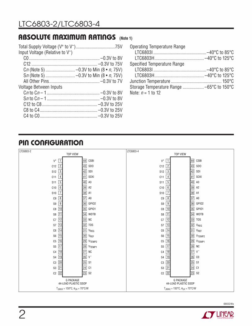
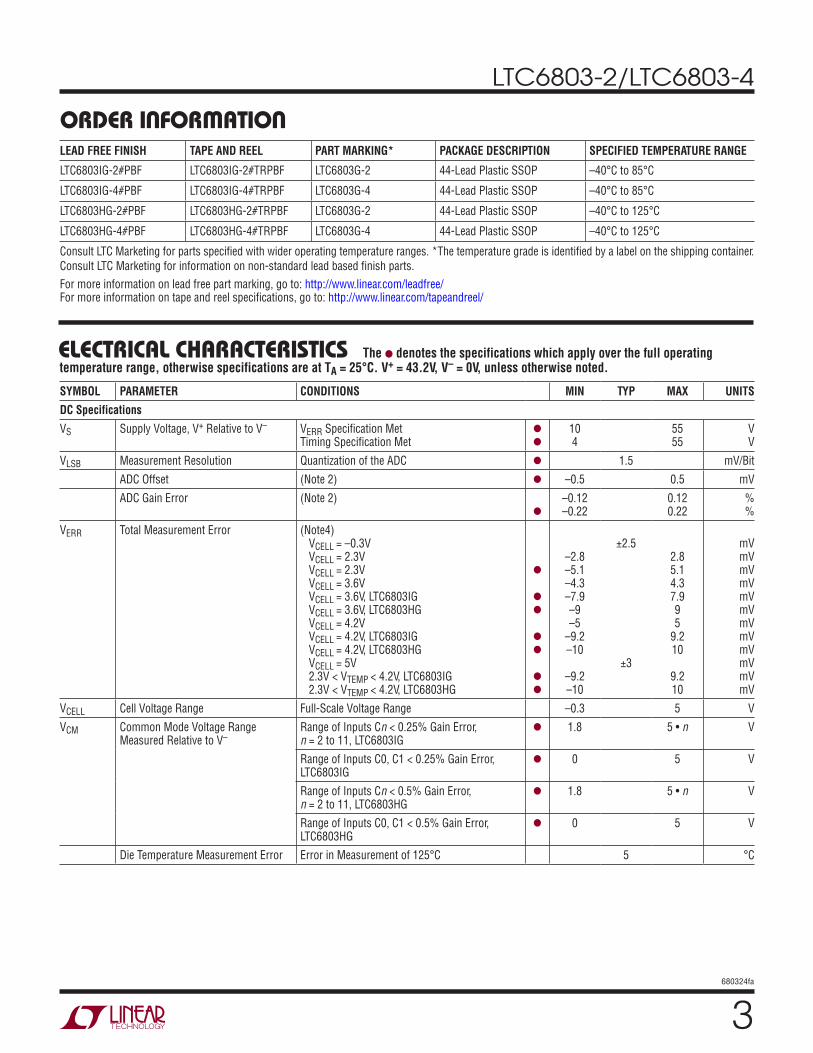
ABSOLUTE MAXIMUM RATINGSTotal Supply Voltage (V+ to V–) .................................75VInput Voltage (Relative to V–) C0 ............................................................ –0.3V to 8V C12 ........................................................ –0.3V to 75V Cn (Note 5) ......................... –0.3V to Min (8 • n, 75V) Sn (Note 5) ......................... –0.3V to Min (8 • n, 75V) All Other Pins ........................................... –0.3V to 7VVoltage Between Inputs Cn to Cn – 1 ............................................. –0.3V to 8V Sn to Cn – 1 ............................................. –0.3V to 8V C12 to C8 ............................................... –0.3V to 25V C8 to C4 ................................................. –0.3V to 25V C4 to C0 ................................................. –0.3V to 25V
(Note 1)
Operating Temperature Range LTC6803I .............................................–40°C to 85°C LTC6803H .......................................... –40°C to 125°CSpecified Temperature Range LTC6803I .............................................–40°C to 85°C LTC6803H .......................................... –40°C to 125°CJunction Temperature ........................................... 150°CStorage Temperature Range .................. –65°C to 150°CNote: n = 1 to 12
LTC6803-2 LTC6803-4
1
2
3
4
5
6
7
8
9
10
11
12
13
14
15
16
17
18
19
20
21
22
TOP VIEW
G PACKAGE44-LEAD PLASTIC SSOP
44
43
42
41
40
39
38
37
36
35
34
33
32
31
30
29
28
27
26
25
24
23
V+
C12
S12
C11
S11
C10
S10
C9
S9
C8
S8
C7
S7
C6
S6
C5
S5
C4
S4
C3
S3
C2
CSBI
SDO
SDI
SCKI
A3
A2
A1
A0
GPIO2
GPIO1
WDTB
NC
TOS
VREG
VREF
VTEMP2
VTEMP1
NC
V–
S1
C1
S2
TJMAX = 150°C, θJA = 70°C/W
1
2
3
4
5
6
7
8
9
10
11
12
13
14
15
16
17
18
19
20
21
22
TOP VIEW
G PACKAGE44-LEAD PLASTIC SSOP
44
43
42
41
40
39
38
37
36
35
34
33
32
31
30
29
28
27
26
25
24
23
V+
C12
S12
C11
S11
C10
S10
C9
S9
C8
S8
C7
S7
C6
S6
C5
S5
C4
S4
C3
S3
C2
CSBI
SDO
SDI
SCKI
A3
A2
A1
A0
GPIO2
GPIO1
WDTB
TOS
VREG
VREF
VTEMP2
VTEMP1
NC
V–
C0
S1
C1
S2
TJMAX = 150°C, θJA = 70°C/W
PIN CONFIGURATION
LTC6803-2/LTC6803-4
3680324fa
ORDER INFORMATIONLEAD FREE FINISH TAPE AND REEL PART MARKING* PACKAGE DESCRIPTION SPECIFIED TEMPERATURE RANGE
LTC6803IG-2#PBF LTC6803IG-2#TRPBF LTC6803G-2 44-Lead Plastic SSOP –40°C to 85°C
LTC6803IG-4#PBF LTC6803IG-4#TRPBF LTC6803G-4 44-Lead Plastic SSOP –40°C to 85°C
LTC6803HG-2#PBF LTC6803HG-2#TRPBF LTC6803G-2 44-Lead Plastic SSOP –40°C to 125°C
LTC6803HG-4#PBF LTC6803HG-4#TRPBF LTC6803G-4 44-Lead Plastic SSOP –40°C to 125°C
Consult LTC Marketing for parts specified with wider operating temperature ranges. *The temperature grade is identified by a label on the shipping container.Consult LTC Marketing for information on non-standard lead based finish parts.For more information on lead free part marking, go to: http://www.linear.com/leadfree/ For more information on tape and reel specifications, go to: http://www.linear.com/tapeandreel/
ELECTRICAL CHARACTERISTICS The l denotes the specifications which apply over the full operating temperature range, otherwise specifications are at TA = 25°C. V+ = 43.2V, V– = 0V, unless otherwise noted.
SYMBOL PARAMETER CONDITIONS MIN TYP MAX UNITS
DC Specifications
VS Supply Voltage, V+ Relative to V– VERR Specification Met Timing Specification Met
l
l
10 4
55 55
V V
VLSB Measurement Resolution Quantization of the ADC l 1.5 mV/Bit
ADC Offset (Note 2) l –0.5 0.5 mV
ADC Gain Error (Note 2)
l
–0.12 –0.22
0.12 0.22
% %
VERR Total Measurement Error (Note4) VCELL = –0.3V VCELL = 2.3V VCELL = 2.3V VCELL = 3.6V VCELL = 3.6V, LTC6803IG VCELL = 3.6V, LTC6803HG VCELL = 4.2V VCELL = 4.2V, LTC6803IG VCELL = 4.2V, LTC6803HG VCELL = 5V 2.3V < VTEMP < 4.2V, LTC6803IG 2.3V < VTEMP < 4.2V, LTC6803HG
l
l
l
l
l
l
l
–2.8 –5.1 –4.3 –7.9 –9 –5
–9.2 –10
–9.2 –10
±2.5
±3
2.8 5.1 4.3 7.9 9 5
9.2 10
9.2 10
mV mV mV mV mV mV mV mV mV mV mV mV
VCELL Cell Voltage Range Full-Scale Voltage Range –0.3 5 V
VCM Common Mode Voltage Range Measured Relative to V–
Range of Inputs Cn < 0.25% Gain Error, n = 2 to 11, LTC6803IG
l 1.8 5 • n V
Range of Inputs C0, C1 < 0.25% Gain Error, LTC6803IG
l 0 5 V
Range of Inputs Cn < 0.5% Gain Error, n = 2 to 11, LTC6803HG
l 1.8 5 • n V
Range of Inputs C0, C1 < 0.5% Gain Error, LTC6803HG
l 0 5 V
Die Temperature Measurement Error Error in Measurement of 125°C 5 °C
LTC6803-2/LTC6803-4
4680324fa
ELECTRICAL CHARACTERISTICS The l denotes the specifications which apply over the full operating temperature range, otherwise specifications are at TA = 25°C. V+ = 43.2V, V– = 0V, unless otherwise noted.
SYMBOL PARAMETER CONDITIONS MIN TYP MAX UNITS
VREF Reference Pin Voltage RLOAD = 100k to V–
l
3.020 3.015
3.065 3.065
3.110 3.115
V V
Reference Voltage Temperature Coefficient
8 ppm/°C
Reference Voltage Thermal Hysteresis 25°C to 85°C and 25°C to –40°C 100 ppm
Reference Voltage Long-Term Drift 60 ppm/√kHr
VREF2 2nd Reference Voltage
l
2.25 2.1
2.5 2.5
2.75 2.9
V V
VREG Regulator Pin Voltage 10V < V+ < 50V, No Load ILOAD = 4mA
l
l
4.5 4.5
5.0 5.0
5.5 V V
Regulator Pin Short-Circuit Limit l 8 mA
IB Input Bias Current In/Out of Pins C1 Through C12 When Measuring Cell When Not Measuring Cell
–10
1
10
µA nA
IS Supply Current, Measure Mode (Note 7)
Current Into the V+ Pin When Measuring Continuous Measuring (CDC = 2) Continuous Measuring (CDC = 2) Measure Every 130ms (CDC = 5) Measure Every 500ms (CDC = 6) Measure Every 2 Seconds (CDC = 7)
l
l
l
l
620 600 190 140 55
780 780 250 175 70
1000 1150 360 250 105
µA µA µA µA µA
IQS Supply Current, Standby Current Into V+ Pin When In Standby, All Serial Port Pin at Logic “1” LTC6803IG LTC6803HG
l
l
8 6 6
12
12 12
16.5
18 19
µA
µA µA
ISD Supply Current, Hardware Shutdown Current Out of V–, VC12 = 43.2V, V+ Floating (Note 8)
l 0.001 1 µA
Discharge Switch-On Resistance VCELL > 3V (Note 3) l 10 20 Ω
IOW Current Used for Open-Wire Detection l 70 110 140 µA
Thermal Shutdown Temperature 145 °C
Thermal Shutdown Hysteresis 5 °C
Voltage Mode Timing Specifications
tCYCLE Measurement Cycling Time Required to Measure 12 Cells Time Required to Measure 10 Cells Time Required to Measure 3 Temperatures Time Required to Measure 1 Cell or Temperature
l
l
l
l
11 9
2.8 1.0
13 11 3.4 1.2
15 13 4.1 1.4
ms ms ms ms
t1 SDI Valid to SCKI Rising Setup l 10 ns
t2 SDI Valid to SCKI Rising Hold l 250 ns
t3 SCKI Low l 400 ns
t4 SCKI High l 400 ns
t5 CSBI Pulse Width l 400 ns
t6 CSBI Falling to SCKI Rising l 100 ns
t7 CSBI Falling to SDO Valid l 100 ns
t8 SCKI Falling to SDO Valid l 250 ns
Clock Frequency l 1 MHz
Watchdog Timer Timeout Period l 1 2.5 Seconds
LTC6803-2/LTC6803-4
5680324fa
Note 1: Stresses beyond those listed under Absolute Maximum Ratings may cause permanent damage to the device. Exposure to any Absolute Maximum Rating condition for extended periods may affect device reliability and lifetime.Note 2: The ADC specifications are guaranteed by the Total Measurement Error (VERR) specification.Note 3: Due to the contact resistance of the production tester, this specification is tested to relaxed limits. The 20Ω limit is guaranteed by design.Note 4: VCELL refers to the voltage applied across Cn to Cn – 1 for n = 1 to 12. VTEMP refers to the voltage applied from VTEMP1 or VTEMP2 to V–.
Note 5: These absolute maximum ratings apply provided that the voltage between inputs do not exceed the absolute maximum ratings.Note 6: Supply current is tested during continuous measuring. The supply current during periodic measuring (130ms, 500ms, 2s) is guaranteed by design.Note 7: The CDC = 5, 6 and 7 supply currents are not measured. They are guaranteed by the CDC = 2 supply current measurement.Note 8: Limit is determined by high speed automated test capability.
ELECTRICAL CHARACTERISTICS The l denotes the specifications which apply over the full operating temperature range, otherwise specifications are at TA = 25°C. V+ = 43.2V, V– = 0V, unless otherwise noted.
SYMBOL PARAMETER CONDITIONS MIN TYP MAX UNITS
Voltage Mode Digital I/O
VIH Digital Input Voltage High Pins SCKI, SDI and CSBI l 2 V
VIL Digital Input Voltage Low Pins SCKI, SDI and CSBI l 0.8 V
VOL Digital Output Voltage Low Pin SDO, Sinking 500µA l 0.3 V
IIN Digital Input Current VMODE, TOS, SCKI, SDI, CSBI l 10 µA
TYPICAL PERFORMANCE CHARACTERISTICS
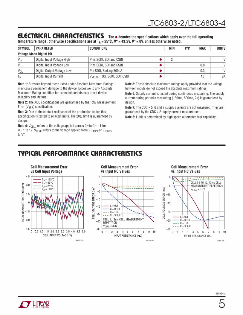
Cell Measurement Error vs Cell Input Voltage
Cell Measurement Error vs Input RC Values
Cell Measurement Error vs Input RC Values
CELL INPUT VOLTAGE (V)
–4.5
TOTA
L UN
ADJU
STED
ERR
OR (m
V)
–1.5
1.5
4.5
–3.0
0
3.0
1.0 2.0 3.0 4.0
680324 G01
5.00.50 1.5 2.5 3.5 4.5
TA = 125°CTA = 85°CTA = 25°CTA = –40°C
INPUT RESISTANCE (kΩ)0
–30
CELL
VOL
TAGE
ERR
OR (m
V)
–25
–15
–10
–5
5
1 5 7
680324 G02
–20
0
4 9 102 3 6 8
C = 0µFC = 0.1µFC = 1µFC = 3.3µF
CELL 1, 13ms CELL MEASUREMENT REPETITIONVCELL = 3.3V
INPUT RESISTANCE (kΩ)0
–30
CELL
VOL
TAGE
ERR
OR (m
V)
–25
–15
–10
–5
0
1 5 7
680324 G03
–20
4 9 102 3 6 8
C = 0µFC = 0.1µFC = 1µFC = 3.3µF
CELLS 2 TO 12, 13ms CELL MEASUREMENT REPETITIONVCELL = 3.3V
LTC6803-2/LTC6803-4
6680324fa
TYPICAL PERFORMANCE CHARACTERISTICS
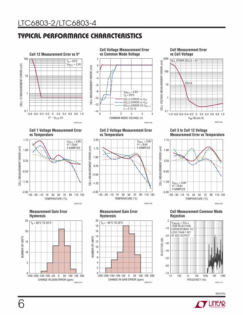
Cell Voltage Measurement Error vs Common Mode Voltage
Cell Measurement Error vs Cell Voltage
Cell 1 Voltage Measurement Error vs Temperature
Cell 12 Measurement Error vs V+
Cell 2 Voltage Measurement Error vs Temperature
Cell 3 to Cell 12 Voltage Measurement Error vs Temperature
Measurement Gain Error Hysteresis
Cell Measurement Common Mode Rejection
Measurement Gain Error Hysteresis
V+ – VC12 (V)–0.8 –0.6 –0.4
CELL
12
MEA
SURE
MEN
T ER
ROR
(mV)
1
10
100
–0.2 0 0.2 0.4 0.6 1.00.8
680324 G04
0.1
TA = 25°CVCELL = 3.3V
COMMON MODE VOLTAGE (V)0
CELL
MEA
SURE
MEN
T ER
ROR
(mV)
–8
–6
–4
3 5
680324 G05
–10
–12
–141 2 4
–2
0
2
CELL2 ERROR vs VC1CELL3 ERROR vs VC2CELLn ERROR VS VCn–1, n = 4 TO 12
VCELL = 3.6VTA = 25°C
VIN CELL6 (V)
1
CELL
VOL
TAGE
MEA
SURE
MEN
T ER
ROR
(mV)
10
100
1000
–1.0 –0.2 0.2 0.60.1
–0.6 1.0–0.4 0 0.4–0.8 0.8
680324 G06
CELL6
ALL OTHER CELLS = 3V
TEMPERATURE (°C)–50
–2.00
CELL
MEA
SURE
MEN
T ER
ROR
(mV)
–1.25
0.25
1.00
1.75
–10 30 50 130
680324 G07
–0.50
–30 10 70 90 110
VCELL = 0.8VV+ = 9.6V4 SAMPLES
TEMPERATURE (°C)–50
–2.00
CELL
MEA
SURE
MEN
T ER
ROR
(mV)
–1.25
0.25
1.00
2.50
1.75
–10 30 50 130
680324 G08
–0.50
–30 10 70 90 110
VCELL = 0.8VV+ = 9.6V4 SAMPLES
TEMPERATURE (°C)–50
–2.00
CELL
MEA
SURE
MEN
T ER
ROR
(mV)
–1.25
0.25
1.00
1.75
–10 30 50 130
680324 G09
–0.50
–30 10 70 90 110
VCELL = 0.8VV+ = 9.6V4 SAMPLES
CHANGE IN GAIN ERROR (ppm)–250
NUM
BER
OF U
NITS
25
20
15
10
5
0–50 150–150 50
680324 G10
200–100 100–200 0
TA = 85°C TO 25°C
CHANGE IN GAIN ERROR (ppm)–250
NUM
BER
OF U
NITS
20
16
12
8
4
18
14
10
6
2
0–50 150–150 50
680324 G11
200–100 100–200 0
TA = –45°C TO 25°C0
–10
–30
–50
–20
–40
–60
–70
FREQUENCY (Hz)
REJE
CTIO
N (d
B)
680324 G12
10 10k 10M1M100k1k100
VCM(IN) = 5VP-P72dB REJECTION CORRESPONDS TO LESS THAN 1 BITAT ADC OUTPUT
LTC6803-2/LTC6803-4
7680324fa
TYPICAL PERFORMANCE CHARACTERISTICS
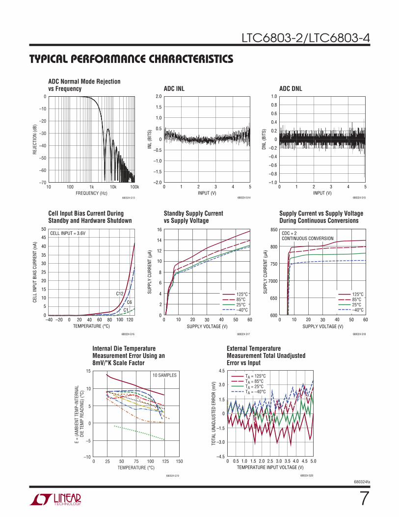
Internal Die Temperature Measurement Error Using an 8mV/°K Scale Factor
External Temperature Measurement Total Unadjusted Error vs Input
ADC INL ADC DNL
Cell Input Bias Current During Standby and Hardware Shutdown
ADC Normal Mode Rejection vs Frequency
Standby Supply Current vs Supply Voltage
Supply Current vs Supply Voltage During Continuous Conversions
0
–10
–30
–50
–20
–40
–60
–70
FREQUENCY (Hz)
REJE
CTIO
N (d
B)
680324 G13
10 10k 100k1k100INPUT (V)
0
INL
(BIT
S)
2.0
1.5
0.5
1.0
0
–1.0
–0.5
–1.5
–2.01 2 4
680324 G14
53INPUT (V)
0
DNL
(BIT
S)
1.0
0.8
0.2
0.4
0.6
0
–0.6
–0.4
–0.2
–0.8
–1.01 2 4
680324 G15
53
TEMPERATURE (°C)–40
0
CELL
INPU
T BI
AS C
URRE
NT (n
A)
5
15
20
25
50
35
0 40 60
680324 G16
10
40
45
30
–20 20 80 100 120
C12
C6
C1
CELL INPUT = 3.6V
SUPPLY VOLTAGE (V)0
SUPP
LY C
URRE
NT (µ
A)
6
8
10
30 50
680324 G17
4
2
010 20 40
12
14
16
60
125°C85°C25°C–40°C
SUPPLY VOLTAGE (V)0
SUPP
LY C
URRE
NT (µ
A)
650
7000
30 50
680324 G18
60010 20 40
750
800
850
60
125°C85°C25°C–40°C
CDC = 2CONTINUOUS CONVERSION
TEMPERATURE INPUT VOLTAGE (V)
–4.5
TOTA
L UN
ADJU
STED
ERR
OR (m
V)
–1.5
1.5
4.5
–3.0
0
3.0
1.0 2.0 3.0 4.0
680324 G20
5.00.50 1.5 2.5 3.5 4.5
TA = 125°CTA = 85°CTA = 25°CTA = –40°C
TEMPERATURE (°C)0
–10
E =
(AM
BIEN
T TE
MP-
INTE
RNAL
DI
E TE
MP
READ
ING)
(°C)
–5
0
5
10
15
25 50 75 100
680324 G19
125 150
10 SAMPLES
LTC6803-2/LTC6803-4
8680324fa
TYPICAL PERFORMANCE CHARACTERISTICS
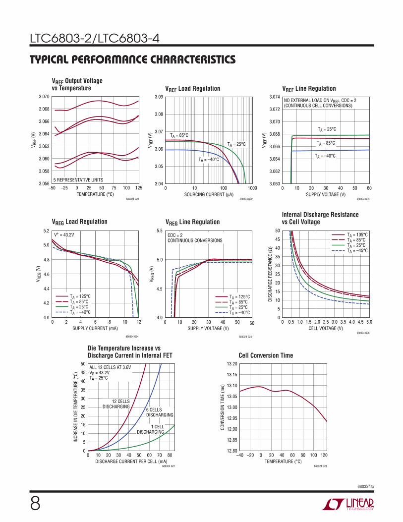
VREF Line Regulation
VREG Load Regulation
VREF Load RegulationVREF Output Voltage vs Temperature
VREG Line RegulationInternal Discharge Resistance vs Cell Voltage
Die Temperature Increase vs Discharge Current in Internal FET Cell Conversion Time
TEMPERATURE (°C)–50
V REF
(V)
3.070
3.068
3.064
3.060
3.066
3.062
3.058
3.056500 100
680324 G21
12525–25 75
5 REPRESENTATIVE UNITS
SOURCING CURRENT (µA)0
V REF
(V)
3.09
3.08
3.07
3.06
3.04
3.05
10 100
680324 G22
1000
TA = 85°C
TA = –40°C
TA = 25°C
SUPPLY VOLTAGE (V)0
V REF
(V)
3.074
3.072
3.070
3.068
3.066
3.064
3.062
3.06020 4010 30 50
680324 G23
60
TA = 85°C
TA = –40°C
TA = 25°C
NO EXTERNAL LOAD ON VREF, CDC = 2 (CONTINUOUS CELL CONVERSIONS)
SUPPLY CURRENT (mA)0
4.0
V REG
(V)
4.2
4.4
4.6
4.8
5.2
2 4 6 8
680324 G24
10 12
5.0
TA = 125°CTA = 85°CTA = 25°CTA = –40°C
V+ = 43.2V
SUPPLY VOLTAGE (V)0
4.0
V REG
(V)
4.5
5.0
5.5
10 20 30 40
680324 G25
50 60
TA = 125°CTA = 85°CTA = 25°CTA = –40°C
CDC = 2CONTINUOUS CONVERSIONS
CELL VOLTAGE (V)0
DISC
HARG
E RE
SIST
ANCE
(Ω)
50
5
45
35
25
15
40
30
20
10
02.5 4.51.5 3.5
680324 G26
5.02.0 4.01.0 3.00.5
TA = 105°CTA = 85°CTA = 25°CTA = –45°C
DISCHARGE CURRENT PER CELL (mA)0
INCR
EASE
IN D
IE T
EMPE
RATU
RE (°
C)
50
5
45
35
25
15
40
30
20
10
040 8020 60
680324 G27
30 7010 50
1 CELLDISCHARGING
6 CELLSDISCHARGING
12 CELLSDISCHARGING
ALL 12 CELLS AT 3.6VVS = 43.2VTA = 25°C
TEMPERATURE (°C)–40
CONV
ERSI
ON T
IME
(ms)
13.20
13.15
13.10
13.05
13.00
12.80
12.85
12.90
12.95
20–20 400 80 10060
680324 G28
120
LTC6803-2/LTC6803-4
9680324fa
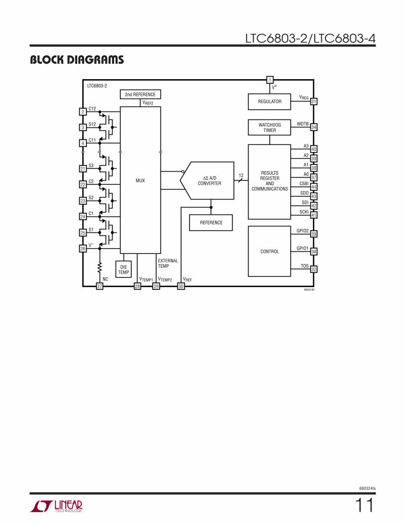
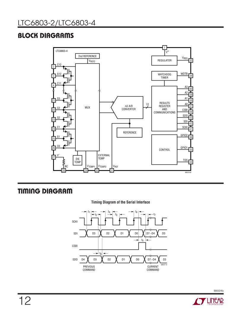
To ensure pin compatibility with LTC6802-2, the LTC6803-2 is configured such that the bottom cell input (C0) is con-nected internally to the negative supply voltage (V–). The LTC6803-4 offers a unique pinout with an input for the bottom cell (C0). This simple functional difference offers the possibility for enhanced cell 1 measurement accuracy, enhanced SPI noise tolerance and simplified wiring. More information is provided in the Applications Information section entitled Advantages of Kelvin Connection for C0.
V+ (Pin 1): Positive Power Supply. Pin 1 can be tied to the most positive potential in the battery stack or an isolated power supply. V+ must be greater than the most positive potential in the battery stack under normal operation. With an isolated power supply, LTC6803 can be turned off by simply shutting down V+.
C12, C11, C10, C9, C8, C7, C6, C5, C4, C3, C2, C1 (Pins 2, 4, 6, 8, 10, 12, 14, 16, 18, 20, 22, 24): C1 through C12 are the inputs for monitoring battery cell voltages. The negative terminal of the bottom cell should be tied to the V– pin for the LTC6803-2, and the C0 pin for the LTC6803-4. The next lowest potential is tied to C1 and so forth. See the figures in the Applications Information section for more details on connecting batteries to the LTC6803-2 and LTC6803-4. The LTC6803 can monitor a series connection of up to 12 cells. Each cell in a series connection must have a common mode voltage that is greater than or equal to the cells below it. 100mV negative voltages are permitted.
C0 (Pin 26 on LTC6803-4): Negative Terminal of the Bot-tom Battery Cell. C0 and V– form a Kelvin connection to eliminate effect of voltage drop at the V– trace.
S12, S11, S10, S9, S8, S7, S6, S5, S4, S3, S2, S1 (Pins 3, 5, 7, 9, 11, 13, 15, 17, 19, 21, 23, 25): S1 though S12 pins are used to balance battery cells. If one cell in a series becomes overcharged, an S output can be used to discharge the cell. Each S output has an internal N-channel MOSFET for discharging. See the Block Diagram. The NMOS has a maximum on-resistance of 20Ω. An external resistor
PIN FUNCTIONSshould be connected in series with the NMOS to dissipate heat outside of the LTC6803 package. When using the internal MOSFETs to discharge cells, the die temperature should be monitored. See Power Dissipation and Thermal Shutdown in the Applications Information section. The S pins also feature an internal pull-up PMOS. This allows the S pins to be used to drive the gates of external MOSFETs for higher discharge capability.
V– (Pin 26 on LTC6803-2/Pin 27 on LTC6803-4): Connect V– to the most negative potential in the series of cells.
NC (Pin 27 on LTC6803-2/Pin 28 on LTC6803-4): This pin is not used and is internally connected to V– through 10Ω. It can be left unconnected or connected to V– on the PCB.
VTEMP1, VTEMP2 (Pins 28, 29 on LTC6803-2/Pins 29, 30, on LTC6803-4): Temperature Sensor Inputs. The ADC will measure the voltage on VTEMPn with respect to V– and store the result in the TMP register. The ADC measurements are relative to the VREF pin voltage. Therefore a simple thermistor and resistor combination connected to the VREF pin can be used to monitor temperature. The VTEMP inputs can also be general purpose ADC inputs.
VREF (Pin 30 on LTC6803-2/Pin 31 on LTC6803-4): 3.065V Voltage Reference Output. This pin should be bypassed with a 1µF capacitor. The VREF pin can drive a 100k resis-tive load connected to V–. Larger loads should be buffered with an LT6003 op amp, or a similar device.
VREG (Pin 31 on LTC6803-2/Pin 32 on LTC6803-4): Linear Voltage Regulator Output. This pin should be bypassed with a 1µF capacitor. The VREG is capable of sourcing up to 4mA to an external load. The VREG pin does not sink current.
TOS (Pin 32 on LTC6803-2/Pin 33 on LTC6803-4): Top of Stack Input. The TOS pin can be tied to VREG or V– for the LTC6803. The state of the TOS pin alters the operation of the SDO pin in the toggle polling mode. See the Serial Port description.
NC (Pin 33 on LTC6803-2): No Connection.
LTC6803-2/LTC6803-4
10680324fa
PIN FUNCTIONSWDTB (Pin 34): Watchdog Timer Output (Active Low). If there is no valid command received in 1 to 2.5 seconds, the WDTB output is asserted. The WDTB pin is an open-drain NMOS output. When asserted it pulls the output down to V– and resets the configuration register to its default state.
GPIO1, GPIO2 (Pins 35, 36): General Purpose Input/Output. By writing a “0” to a GPIO configuration register bit, the open-drain output is activated and the pin is pulled to V–. By writing a logic “1” to the configuration register bit, the corresponding GPIO pin is high impedance. An external resistor is required to pull the pin up to VREG. By reading the configuration register locations GPIO1 and GPIO2, the state of the pins can be determined. For example, if a “0” is written to register bit GPIO1, a “0” is always read back because the output N-channel MOSFET pulls Pin 35 to V–. If a “1” is written to register bit GPIO1, the pin becomes high impedance. Either a “1” or a “0” is read back, depending on the voltage present at Pin 35. The GPIOs makes it possible to turn-on/off circuitry around the LTC6803-4, or read logic values from a circuit around the LTC6803-4. The GPIO pins should be connected to V– if not used.
A0, A1, A2, A3 (Pins 37, 38, 39, 40): Address Inputs. These pins are tied to VREG or V–. The state of the address pins (VREG = 1, V– = 0) determines the LTC6803 address. See Address Commands in the Serial Port subsection of the Applications Information section.
SCKI (Pin 41): Serial Clock Input. The SCKI pin inter-faces to any logic gate (TTL levels). See Serial Port in the Applications Information section.
SDI (Pin 42): Serial Data Input. The SDI pin interfaces to any logic gate (TTL levels). See Serial Port in the Applica-tions Information section.
SDO (Pin 43): Serial Data Output. The SDO pin is an NMOS open-drain output. A pull-up resistor is needed on SDO. See Serial Port in the Applications Information section.
CSBI (Pin 44): Chip Select (Active Low) Input. The CSBI pin interfaces to any logic gate (TTL levels). See Serial Port in the Applications Information section.
LTC6803-2/LTC6803-4
11680324fa
BLOCK DIAGRAMS
2C12
VREF2
LTC6803-2
4C11
3S12
2237
C2
21S3
24C1
23S2
26V–
27 28
NC VTEMP1
25S1
MUX12
CSBI
A0
44SDO
43
42SDI
40A3
34WDTB
39A2
38A1
41SCKI
∆Σ A/DCONVERTER
RESULTSREGISTER
ANDCOMMUNICATIONS
68032 BD
32TOS
39GPIO2
38GPIO1
CONTROL
WATCHDOGTIMER
31
1
VREG
V+
REGULATOR
REFERENCE
DIETEMP
VTEMP2
EXTERNALTEMP
29
VREF
30
2nd REFERENCE
LTC6803-2/LTC6803-4
12680324fa
BLOCK DIAGRAMS
TIMING DIAGRAMTiming Diagram of the Serial Interface
2C12
LTC6803-4
4C11
3S12
2244
37C2
21S3
24C1
23S2
26C0
27
29
V–
VTEMP1
28NC
25S1
MUX12
CSBI
43SDO
42SDI
40A3
34WDTB
39A2
38A1
A0
41SCKI
∆Σ A/DCONVERTER
RESULTSREGISTER
ANDCOMMUNICATIONS
68033 BD
33TOS
36GPIO2
35GPIO1
CONTROL
WATCHDOGTIMER
32
1
VREG
V+
REGULATOR
REFERENCE
DIETEMP
VTEMP2
EXTERNALTEMP
30
VREF
31
VREF2
2nd REFERENCE
SCKI
t1
t8
t4 t6t3
t5
t7t2
SDI
SDO D4 D3 D2 D1 D0 D3
68034 TD
D7···D4
D3 D2 D1 D0 D3D7···D4
PREVIOUSCOMMAND
CURRENTCOMMAND
CSBI
LTC6803-2/LTC6803-4
13680324fa
OPERATIONTHEORY OF OPERATION
The LTC6803 is a data acquisition IC capable of mea-suring the voltage of 12 series connected battery cells. An input multiplexer connects the batteries to a 12-bit delta-sigma analog-to-digital converter (ADC). An internal 8ppm/°C voltage reference combined with the ADC give the LTC6803 its outstanding measurement accuracy. The inherent benefits of the delta-sigma ADC versus other types of ADCs (e.g., successive approximation) are explained in Advantages of Delta-Sigma ADCs in the Applications Information section.
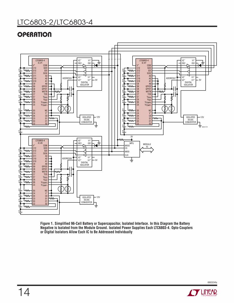
Communication between the LTC6803 and a host processor is handled by a SPI compatible serial interface. Multiple LTC6803s can be connected to a single serial interface. As shown in Figure 1, the LTC6803-2s or LTC6803-4s are isolated from one another using digital isolators. A unique addressing scheme allows all the LTC6803-2s or LTC6803-4s to connect to the same serial port of the host processor. Further explanation of the LTC6803-2/LTC6803-4 can be found in the Serial Port section of the data sheet.
The LTC6803 also contains circuitry to balance cell voltages. Internal MOSFETs can be used to discharge cells. These internal MOSFETs can also be used to control external balancing circuits. Figure 1 illustrates cell balancing by internal discharge. Figure 3 shows the S pin controlling an external balancing circuit. It is important to note that the LTC6803 makes no decisions about turning on/off the internal MOSFETs. This is completely controlled by the host processor. The host processor writes values to a configuration register inside the LTC6803 to control the switches. The watchdog timer on the LTC6803 can be used to turn off the discharge switches if communication with the host processor is interrupted.
Since the LTC6803-4 separates C0 and V–, C0 can have higher potential than V–. This feature is very useful for super capacitors and fuel cells whose voltages can go to zero or slightly negative. In such a case, the stacked cells can’t power the LTC6803-4. In Figure 1, an isolated 36V and –3.6V provides power to each LTC6803-4. This allows the C1 to C12 pins to go up to 3.6V below C0.
The LTC6803 has three modes of operation: hardware shutdown, standby and measure. Hardware shutdown is a true zero power mode. Standby mode is a power saving state where all circuits except the serial interface are turned off. In measure mode, the LTC6803 is used to measure cell voltages and store the results in memory. Measure mode will also monitor each cell voltage for overvoltage (OV) and undervoltage (UV) conditions.
HARDWARE SHUTDOWN MODE
The V+ pin can be disconnected from the C pins and the battery pack. If the V+ supply pin is 0V, the LTC6803 will typically draw less than 1nA from the battery cells. All circuits inside the IC are off. It is not possible to com-municate with the IC when V+ = 0V. See the Applications Information section for hardware shutdown circuits.
STANDBY MODE
The LTC6803 defaults (powers up) to standby mode. Standby mode is the lowest supply current state with a supply connected. Standby current is typically 12µA when V+ = 44V. All circuits are turned off except the serial interface and the voltage regulator. For the lowest possible standby current consumption, all SPI logic inputs should be set to logic 1 level. The LTC6803 can be programmed for standby mode by setting the comparator duty cycle configuration bits, CDC[2:0], to 0. If the part is put into standby mode while ADC measurements are in progress, the measure-ments will be interrupted and the cell voltage registers will be in an indeterminate state. To exit standby mode, the CDC bits must be written to a value other than 0.
MEASURE MODE
The LTC6803 is in measure mode when the CDC bits are programmed with a value from 1 to 7. When CDC = 1 the LTC6803 is on and waiting for a start ADC conversion command. When CDC is 2 through 7 the IC monitors each cell voltage and produces an interrupt signal on the SDO pin indicating all cell voltages are within the UV and OV limits. The value of the CDC bits determines how often the cells are monitored, and, how much average supply current is consumed.
LTC6803-2/LTC6803-4
14680324fa
OPERATION
Figure 1. Simplified 96-Cell Battery or Supercapacitor, Isolated Interface. In this Diagram the Battery Negative is Isolated from the Module Ground. Isolated Power Supplies Each LTC6803-4. Opto-Couplers or Digital Isolators Allow Each IC to Be Addressed Individually
+
+
+
+
+
+
+
+
+
+
+
V+
C12S12C11S11C10S10C9S9C8S8C7S7C6S6C5
S5C4S4C3S3C2
CSBISDOSDI
SCKIA3A2A1A0
GPIO2GPIO1WDTB
TOSVREGVREF
VTEMP2VTEMP1
NCV–
C0S1C1S2
LTC6803-4IC #1
V2–
V2–
V2+ 3VADDRESS1
ADDRESS0
OE2
DIGITALISOLATOR
V1–
V1–
V1+
OE1
+
+
+
+
+
+
+
+
+
+
+
+
V+
C12S12C11S11C10S10C9S9C8S8C7S7C6S6C5
S5C4S4C3S3C2
CSBISDOSDI
SCKIA3A2A1A0
GPIO2GPIO1WDTB
TOSVREGVREF
VTEMP2VTEMP1
NCV–
C0S1C1S2
LTC6803-4IC #0
V2–
V2–
V2+ 3V
OE2
DIGITALISOLATOR
V1–
V1–
V1+
OE1
+
+
+
+
+
+
+
+
+
+
+
+
V+
C12S12C11S11C10S10C9S9C8S8C7S7C6S6C5
S5C4S4C3S3C2
CSBISDOSDI
SCKIA3A2A1A0
GPIO2GPIO1WDTB
TOSVREGVREF
VTEMP2VTEMP1
NCV–
C0S1C1S2
LTC6803-4IC #7
V2–
V2–
V2+ 3V
OE2
DIGITALISOLATOR
V1–
V1–
V1+
OE1
680324 F01
MPU
3V
MODULEIO
CSMISO
M0SI
CLK
ADDRESS7
12VISOLATEDDC/DC
CONVERTER
12VISOLATEDDC/DC
CONVERTER
12VISOLATEDDC/DC
CONVERTER
LTC6803-2/LTC6803-4
15680324fa
OPERATIONThere are two methods for indicating the UV/OV inter-rupt status: toggle polling (using a 1kHz output signal) and level polling (using a high or low output signal). The polling methods are described in the Serial Port section. The UV/OV limits are set by the VUV and VOV values in the configuration registers. When a cell voltage exceeds the UV/OV limits a bit is set in the flag register. The UV and OV flag status for each cell can be determined using the Read Flag Register Group.
An ADC measurement can be requested at any time when the IC is in measure mode. To initiate cell voltage measure-ments while in measure mode, a Start A/D Conversion command is sent. After the command has been sent, the LTC6803 will indicate the A/D converter status via toggle polling or level polling (as described in the Serial Port section). During cell voltage measurement commands, the UV and OV flags (within the flag register group) are also updated. When the measurements are complete, the part will continue monitoring UV and OV conditions at the rate designated by the CDC bits. Note that there is a 5µs window during each UV/OV comparison cycle where an ADC measurement request may be missed. This is an unlikely event. For example, the comparison cycle is 2 seconds when CDC = 7. Use the CLEAR command to detect missing ADC commands.
Operating with Less than 12 Cells
If fewer than 12 cells are connected to the LTC6803, the unused input channels must be masked. The MCxI bits in the configuration registers are used to mask channels. In addition, the LTC6803 can be configured to automatically bypass the measurements of the top 2 cells, reducing power consumption and measurement time. If the CELL10 bit is high, the inputs for cell 11 and cell 12 are masked and only the bottom 10-cell voltages will be measured. By default, the CELL10 bit is low, enabling measurement of all 12-cell voltages. Additional information regarding operation with less than 12 cells is provided in the applications section.
ADC RANGE AND OUTPUT FORMAT
The ADC outputs a 12-bit code with an offset of 0x200 (512 decimal). The input voltage can be calculated as:
VIN = (DOUT – 512) • VLSB; VLSB = 1.5mV
where DOUT is a decimal integer.
For example, a 0V input will have an output reading of 0x200. An ADC reading of 0x000 means the input was –0.768V. The absolute ADC measurement range is –0.768V to 5.376V. The resolution is VLSB = 1.5mV = (5.376 + 0.768)/212. The useful range is –0.3V to 5V. This range allows monitoring supercapacitors which could have small negative voltage. Inputs below –0.3V exceed the absolute maximum rating of the C pins. If all inputs are negative, the ADC range is reduced to –0.1V. Inputs above 5V will have noisy ADC readings (see Typical Performance Characteristics).
ADC MEASUREMENTS DURING CELL BALANCING
The primary cell voltage ADC measurement commands (STCVAD and STOWAD) automatically turn off a cell’s discharge switch while its voltage is being measured. The discharge switches for the cell above and the cell below will also be turned off during the measurement. For example, discharge switches S4, S5 and S6 will be off while cell 5 is being measured. The UV/OV comparison conversions in CDC modes 2 through 7 also cause a momentary turn-off of the discharge switch. For example, switches S4, S5 and S6 will be off while cell 5 is checked for a UV/OV condition.
In some systems it may be desirable to allow discharging to continue during cell voltage measurements. The cell voltage ADC conversion commands STCVDC and STOWDC allow the discharge switches to remain on during cell voltage measurements. This feature allows the system to perform a self test to verify the discharge functionality.
LTC6803-2/LTC6803-4
16680324fa
OPERATIONADC REGISTER CLEAR COMMAND
The clear command can be used to clear the cell voltage registers and temperature registers. The clear command will set all registers to 0xFFF. This command is used to make sure conversions are being made. When cell volt-ages are stable, ADC results could stay the same. If a start ADC conversion command is sent to the LTC6803 but the PEC fails to match then the command is ignored and the voltage register contents also will not change. Sending a clear command then reading back register contents is a way to make sure LTC6803 is accepting commands and performing new measurements. The clear command takes 1ms to execute.
ADC CONVERTER SELF TEST
Two self-test commands can be used to verify the func-tionality of the digital portions of the ADC. The self tests also verify the cell voltage registers and temperature monitoring registers. During these self tests a test signal is applied to the ADC. If the circuitry is working properly all cell voltage and temperature registers will contain 0x555 or 0xAAA. The time required for the self-test function is the same as required to measure all cell voltages or all temperature sensors.
MULTIPLEXER AND REFERENCE SELF TEST
The LTC6803 uses a multiplexer to measure the 12 bat-tery cell inputs as well as the temperature signals. A diagnostic command is used to validate the function of the multiplexer, the temperature sensor, and the precision reference circuit. Diagnostic registers will be updated after each diagnostic test. The muxfail bit of the registers will be 1 if the multiplexer self test fails.
A constant voltage generated by the 2nd reference circuit will be measured by the ADC and the results written to the diagnostic register. The voltage reading should be 2.5V ±16%. Readings outside this range indicate a failure of the temperature sensor circuit, the precision reference circuit, or the analog portion of the ADC. The DAGN com-mand executes in 16.4ms, which is the sum of the 12-cell tCYCLE and the 3 temperature tCYCLE. The diagnostic read command can be used to read the registers.
USING THE GENERAL PURPOSE INPUTS/OUTPUTS (GPIO1, GPIO2)
The LTC6803 has two general purpose digital input/output pins. By writing a GPIO configuration register bit to a logic low, the open-drain output can be activated. The GPIOs give the user the ability to turn on/off circuitry around the LTC6803. One example might be a circuit to verify the operation of the system.
When a GPIO configuration bit is written to a logic high, the corresponding GPIO pin may be used as an input. The read back value of that bit will be the logic level that appears at the GPIO pins.
WATCHDOG TIMER CIRCUIT
The LTC6803 includes a watchdog timer circuit. The watchdog timer is on for all modes except CDC = 0. The watchdog timer times out if no valid command is received for 1 to 2.5 seconds. When the watchdog timer circuit times out, the WDTB open-drain output is asserted low and the configuration register bits are reset to their default (power-up) state. In the power-up state, CDC is 0, the S outputs are off and the IC is in the low power standby mode. The WDTB pin remains low until a valid command is received. The watchdog timer provides a means to turn off cell discharging should communications to the MPU be interrupted. There is no need for the watchdog timer at CDC = 0 since discharging is off. The open-drain WDTB output can be wire ORd with other external open-drain signals. Pulling the WDTB signal low will not initiate a watchdog event, but the CNFGO bit 7 will reflect the state of this signal. Therefore, the WDTB pin can be used to monitor external digital events if desired.
SERIAL PORT
Overview
The LTC6803-2/LTC6803-4 has an SPI bus compatible serial port. Devices can be connected in parallel, using digital isolators. Multiple devices are uniquely identified by a part address determined by the A0 to A3 pins. Physical Layer on the LTC6803-2/LTC6803-4, four pins comprise the serial interface: CSBI, SCKI, SDI and SDO. The SDO
LTC6803-2/LTC6803-4
17680324fa
OPERATIONand SDI may be tied together, if desired, to form a single, bi-directional port. Four address pins (A0 to A3) set the part address for address commands. The TOS pin desig-nates the top device (logic high) for polling commands. All interface pins are voltage mode, with voltage levels sensed with respect to the V– supply. See Figure 1.
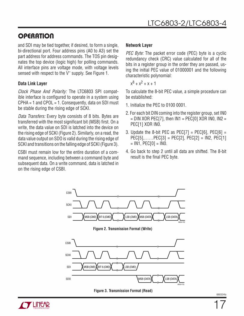
Data Link Layer
Clock Phase And Polarity: The LTC6803 SPI compat-ible interface is configured to operate in a system using CPHA = 1 and CPOL = 1. Consequently, data on SDI must be stable during the rising edge of SCKI.
Data Transfers: Every byte consists of 8 bits. Bytes are transferred with the most significant bit (MSB) first. On a write, the data value on SDI is latched into the device on the rising edge of SCKI (Figure 2). Similarly, on a read, the data value output on SDO is valid during the rising edge of SCKI and transitions on the falling edge of SCKI (Figure 3).
CSBI must remain low for the entire duration of a com-mand sequence, including between a command byte and subsequent data. On a write command, data is latched in on the rising edge of CSBI.
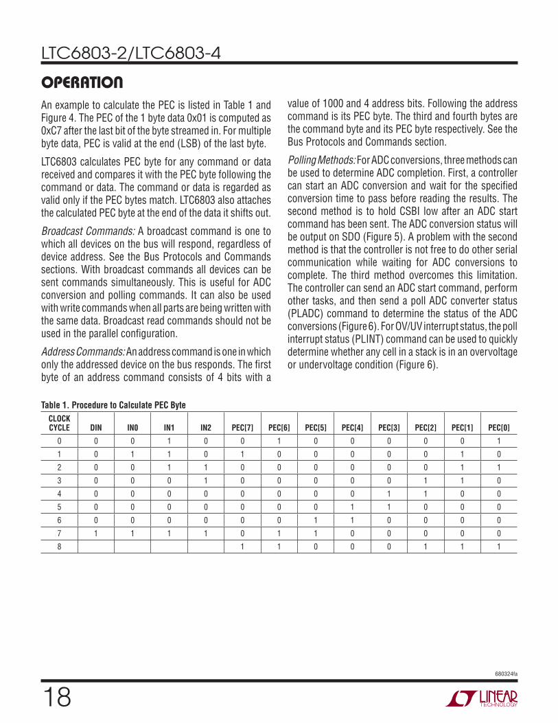
Network Layer
PEC Byte: The packet error code (PEC) byte is a cyclic redundancy check (CRC) value calculated for all of the bits in a register group in the order they are passed, us-ing the initial PEC value of 01000001 and the following characteristic polynomial:
x8 + x2 + x + 1
To calculate the 8-bit PEC value, a simple procedure can be established:
1. Initialize the PEC to 0100 0001.
2. For each bit DIN coming into the register group, set IN0 = DIN XOR PEC[7], then IN1 = PEC[0] XOR IN0, IN2 = PEC[1] XOR IN0.
3. Update the 8-bit PEC as PEC[7] = PEC[6], PEC[6] = PEC[5],……PEC[3] = PEC[2], PEC[2] = IN2, PEC[1] = IN1, PEC[0] = IN0.
4. Go back to step 2 until all data are shifted. The 8-bit result is the final PEC byte.
Figure 2. Transmission Format (Write)
Figure 3. Transmission Format (Read)
SDI MSB (CMD) BIT 6 (CMD) LSB (CMD) MSB (DATA) LSB (DATA)
68034 F02
SCKI
CSBI
SDI
SDO
MSB (CMD) BIT 6 (CMD) LSB (CMD)
MSB (DATA) LSB (DATA)
68034 F03
SCKI
CSBI
LTC6803-2/LTC6803-4
18680324fa
An example to calculate the PEC is listed in Table 1 and Figure 4. The PEC of the 1 byte data 0x01 is computed as 0xC7 after the last bit of the byte streamed in. For multiple byte data, PEC is valid at the end (LSB) of the last byte.
LTC6803 calculates PEC byte for any command or data received and compares it with the PEC byte following the command or data. The command or data is regarded as valid only if the PEC bytes match. LTC6803 also attaches the calculated PEC byte at the end of the data it shifts out.
Broadcast Commands: A broadcast command is one to which all devices on the bus will respond, regardless of device address. See the Bus Protocols and Commands sections. With broadcast commands all devices can be sent commands simultaneously. This is useful for ADC conversion and polling commands. It can also be used with write commands when all parts are being written with the same data. Broadcast read commands should not be used in the parallel configuration.
Address Commands: An address command is one in which only the addressed device on the bus responds. The first byte of an address command consists of 4 bits with a
Table 1. Procedure to Calculate PEC ByteCLOCK CYCLE DIN IN0 IN1 IN2 PEC[7] PEC[6] PEC[5] PEC[4] PEC[3] PEC[2] PEC[1] PEC[0]
0 0 0 1 0 0 1 0 0 0 0 0 1
1 0 1 1 0 1 0 0 0 0 0 1 0
2 0 0 1 1 0 0 0 0 0 0 1 1
3 0 0 0 1 0 0 0 0 0 1 1 0
4 0 0 0 0 0 0 0 0 1 1 0 0
5 0 0 0 0 0 0 0 1 1 0 0 0
6 0 0 0 0 0 0 1 1 0 0 0 0
7 1 1 1 1 0 1 1 0 0 0 0 0
8 1 1 0 0 0 1 1 1
value of 1000 and 4 address bits. Following the address command is its PEC byte. The third and fourth bytes are the command byte and its PEC byte respectively. See the Bus Protocols and Commands section.
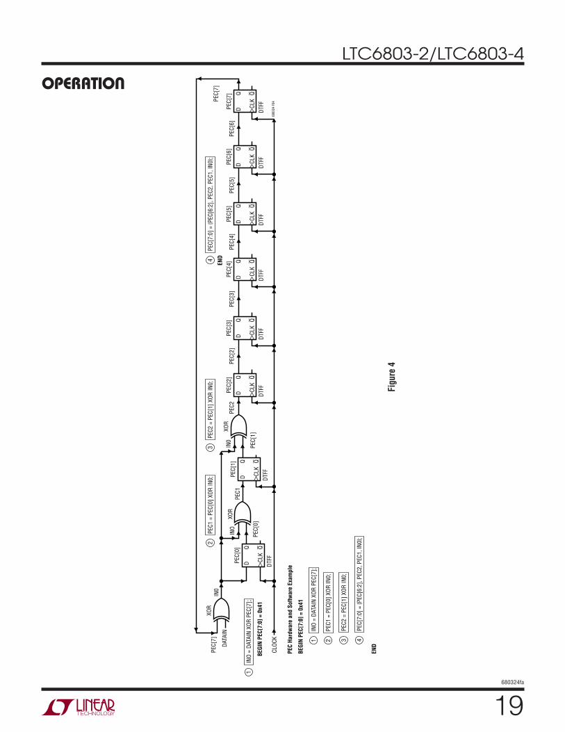
Polling Methods: For ADC conversions, three methods can be used to determine ADC completion. First, a controller can start an ADC conversion and wait for the specified conversion time to pass before reading the results. The second method is to hold CSBI low after an ADC start command has been sent. The ADC conversion status will be output on SDO (Figure 5). A problem with the second method is that the controller is not free to do other serial communication while waiting for ADC conversions to complete. The third method overcomes this limitation. The controller can send an ADC start command, perform other tasks, and then send a poll ADC converter status (PLADC) command to determine the status of the ADC conversions (Figure 6). For OV/UV interrupt status, the poll interrupt status (PLINT) command can be used to quickly determine whether any cell in a stack is in an overvoltage or undervoltage condition (Figure 6).
OPERATION
LTC6803-2/LTC6803-4
19680324fa
OPERATION
Figu
re 4
XOR
BEGI
N PE
C[7:
0] =
0x4
1
PEC
Hard
war
e an
d So
ftwar
e Ex
ampl
e
BEGI
N PE
C[7:
0] =
0x4
1
END
IN0
INO
IN0
PEC2
XOR
XOR
PEC[
0]PE
C[1]
PEC1
PEC[
7]
DATA
IN
CLOC
K
PEC[
0]
CLK
DTFF
DQ Q
PEC[
1]
CLK
DTFF
DQ Q
PEC[
2]
CLK
DTFF
DQ Q
1IN
O =
DATA
IN X
OR P
EC[7
];
1IN
O =
DATA
IN X
OR P
EC[7
];
2PE
C1 =
PEC
[0] X
OR IN
0;
2PE
C1 =
PEC
[0] X
OR IN
0;
3PE
C2 =
PEC
[1] X
OR IN
0;
3PE
C2 =
PEC
[1] X
OR IN
0;
4PE
C[7:
0] =
{PEC
[6:2
], PE
C2, P
EC1,
IN0}
;
4PE
C[7:
0] =
{PEC
[6:2
], PE
C2, P
EC1,
IN0}
;
PEC[
2]PE
C[3]
PEC[
4]
END
PEC[
5]PE
C[6]
PEC[
7]
6803
24 F
04
PEC[
3]
CLK
DTFF
DQ Q
PEC[
4]
CLK
DTFF
DQ Q
PEC[
5]
CLK
DTFF
DQ Q
PEC[
6]
CLK
DTFF
DQ Q
PEC[
7]
CLK
DTFF
DQ Q
LTC6803-2/LTC6803-4
20680324fa
Toggle Polling: Toggle polling allows a robust determina-tion both of device states and of the integrity of the con-nections between the devices in a stack. Toggle polling is enabled when the LVLPL bit is low. After entering a polling command, the data out line will be driven by the slave devices based on their status. When polling for the ADC converter status, data out will be low when any device is busy performing an ADC conversion and will toggle at 1kHz when no device is busy. Similarly, when polling for interrupt status, the output will be low when any device has an interrupt condition and will toggle at 1kHz when none has an interrupt condition.
Toggle Polling—Address Polling: The addressed device drives the SDO line based on its state alone—low for busy/in interrupt, toggling at 1kHz for not busy/not in interrupt.
Toggle Polling—Parallel Broadcast Polling: No part ad-dress is sent, so all devices respond simultaneously. If a device is busy/in interrupt, it will pull SDO low. If a device is not busy/not in interrupt, then it will release the SDO line (TOS = 0) or attempt to toggle the SDO line at 1kHz (TOS = 1).The master controller pulls CSBI high to exit polling.
CSBI
SCKI
SDI
SDO
MSB (CMD) BIT6 (CMD) LSB (PEC)
TOGGLE OR LEVEL POLL
tCYCLE
680324 F05
CSBI
SCKI
SDI
SDO
MSB (CMD) BIT6 (CMD) LSB (PEC)
TOGGLE OR LEVEL POLL680324 F06
Figure 5. Transmission Format (ADC Conversion and Poll)
Figure 6. Transmission Format (PLADC Conversion or PLINT)
Level Polling: Level polling is enabled when the LVLPL bit is high. After entering a polling command, the data out line will be driven by the slave devices based on their status. When polling for the ADC converter status, data out will be low when any device is busy performing an ADC conversion and will be high when no device is busy. Similarly, when polling for interrupt status, the output will be low when any device has an interrupt condition and will be high when none has an interrupt condition.
Level Polling—Address Polling: The addressed device drives the SDO line based on its state alone—pulled low for busy/in interrupt, released for not busy/not in interrupt.
Level polling—Parallel Broadcast Polling: No part address is sent, so all devices respond simultaneously. If a device is busy/in interrupt, it will pull SDO low. If a device is not busy/not in interrupt, then it will release the SDO line. If any device is busy or in interrupt the SDO signal will be low. If all devices are not busy/not in interrupt, the SDO signal will be high. The master controller pulls CSBI high to exit polling.
OPERATION
LTC6803-2/LTC6803-4
21680324fa
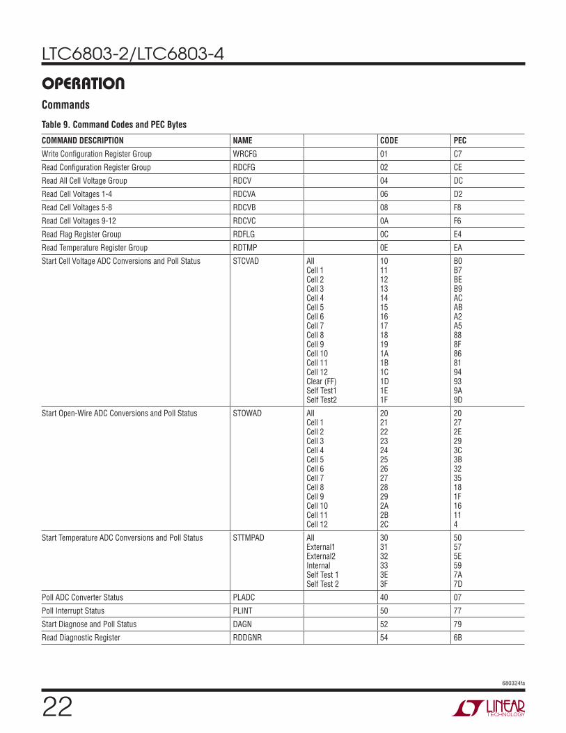
OPERATIONRevision Code
The diagnostic register group contains a 2-bit revision code. If software detection of device revision is neces-sary, then contact the factory for details. Otherwise, the code can be ignored. In all cases, however, the values of all bits must be used when calculating the packet error code (PEC) byte on data reads.
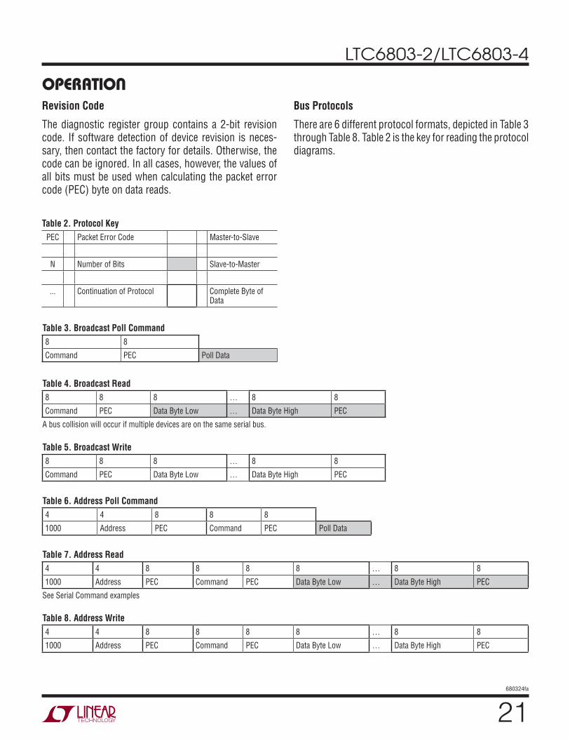
Bus Protocols
There are 6 different protocol formats, depicted in Table 3 through Table 8. Table 2 is the key for reading the protocol diagrams.
Table 6. Address Poll Command 4 4 8 8 8
1000 Address PEC Command PEC Poll Data
Table 7. Address Read 4 4 8 8 8 8 … 8 8
1000 Address PEC Command PEC Data Byte Low … Data Byte High PEC
See Serial Command examples
Table 8. Address Write 4 4 8 8 8 8 … 8 8
1000 Address PEC Command PEC Data Byte Low … Data Byte High PEC
Table 4. Broadcast Read 8 8 8 … 8 8
Command PEC Data Byte Low … Data Byte High PEC
A bus collision will occur if multiple devices are on the same serial bus.
Table 5. Broadcast Write 8 8 8 … 8 8
Command PEC Data Byte Low … Data Byte High PEC
Table 2. Protocol KeyPEC Packet Error Code Master-to-Slave
N Number of Bits Slave-to-Master
... Continuation of Protocol Complete Byte of Data
Table 3. Broadcast Poll Command 8 8
Command PEC Poll Data
LTC6803-2/LTC6803-4
22680324fa
Commands
OPERATION
COMMAND DESCRIPTION NAME CODE PEC
Write Configuration Register Group WRCFG 01 C7
Read Configuration Register Group RDCFG 02 CE
Read All Cell Voltage Group RDCV 04 DC
Read Cell Voltages 1-4 RDCVA 06 D2
Read Cell Voltages 5-8 RDCVB 08 F8
Read Cell Voltages 9-12 RDCVC 0A F6
Read Flag Register Group RDFLG 0C E4
Read Temperature Register Group RDTMP 0E EA
Start Cell Voltage ADC Conversions and Poll Status STCVAD All Cell 1 Cell 2 Cell 3 Cell 4 Cell 5 Cell 6 Cell 7 Cell 8 Cell 9 Cell 10 Cell 11 Cell 12 Clear (FF) Self Test1 Self Test2
10 11 12 13 14 15 16 17 18 19 1A 1B 1C 1D 1E 1F
B0 B7 BE B9 AC AB A2 A5 88 8F 86 81 94 93 9A 9D
Start Open-Wire ADC Conversions and Poll Status STOWAD All Cell 1 Cell 2 Cell 3 Cell 4 Cell 5 Cell 6 Cell 7 Cell 8 Cell 9 Cell 10 Cell 11 Cell 12
20 21 22 23 24 25 26 27 28 29 2A 2B 2C
20 27 2E 29 3C 3B 32 35 18 1F 16 11 4
Start Temperature ADC Conversions and Poll Status STTMPAD All External1 External2 Internal Self Test 1 Self Test 2
30 31 32 33 3E 3F
50 57 5E 59 7A 7D
Poll ADC Converter Status PLADC 40 07
Poll Interrupt Status PLINT 50 77
Start Diagnose and Poll Status DAGN 52 79
Read Diagnostic Register RDDGNR 54 6B
Table 9. Command Codes and PEC Bytes
LTC6803-2/LTC6803-4
23680324fa
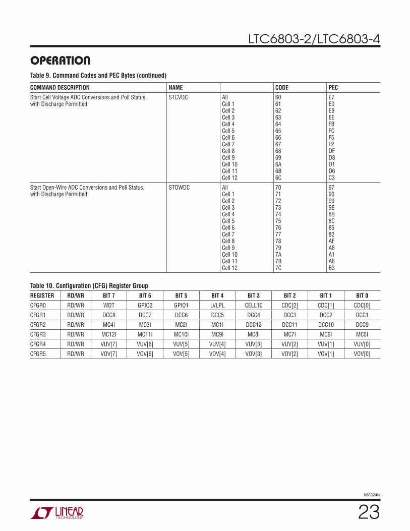
OPERATION
COMMAND DESCRIPTION NAME CODE PEC
Start Cell Voltage ADC Conversions and Poll Status, with Discharge Permitted
STCVDC All Cell 1 Cell 2 Cell 3 Cell 4 Cell 5 Cell 6 Cell 7 Cell 8 Cell 9 Cell 10 Cell 11 Cell 12
60 61 62 63 64 65 66 67 68 69 6A 6B 6C
E7 E0 E9 EE FB FC F5 F2 DF D8 D1 D6 C3
Start Open-Wire ADC Conversions and Poll Status, with Discharge Permitted
STOWDC All Cell 1 Cell 2 Cell 3 Cell 4 Cell 5 Cell 6 Cell 7 Cell 8 Cell 9 Cell 10 Cell 11 Cell 12
70 71 72 73 74 75 76 77 78 79 7A 7B 7C
97 90 99 9E 8B 8C 85 82 AF A8 A1 A6 B3
Table 10. Configuration (CFG) Register GroupREGISTER RD/WR BIT 7 BIT 6 BIT 5 BIT 4 BIT 3 BIT 2 BIT 1 BIT 0
CFGR0 RD/WR WDT GPIO2 GPIO1 LVLPL CELL10 CDC[2] CDC[1] CDC[0]
CFGR1 RD/WR DCC8 DCC7 DCC6 DCC5 DCC4 DCC3 DCC2 DCC1
CFGR2 RD/WR MC4I MC3I MC2I MC1I DCC12 DCC11 DCC10 DCC9
CFGR3 RD/WR MC12I MC11I MC10I MC9I MC8I MC7I MC6I MC5I
CFGR4 RD/WR VUV[7] VUV[6] VUV[5] VUV[4] VUV[3] VUV[2] VUV[1] VUV[0]
CFGR5 RD/WR VOV[7] VOV[6] VOV[5] VOV[4] VOV[3] VOV[2] VOV[1] VOV[0]
Table 9. Command Codes and PEC Bytes (continued)
LTC6803-2/LTC6803-4
24680324fa
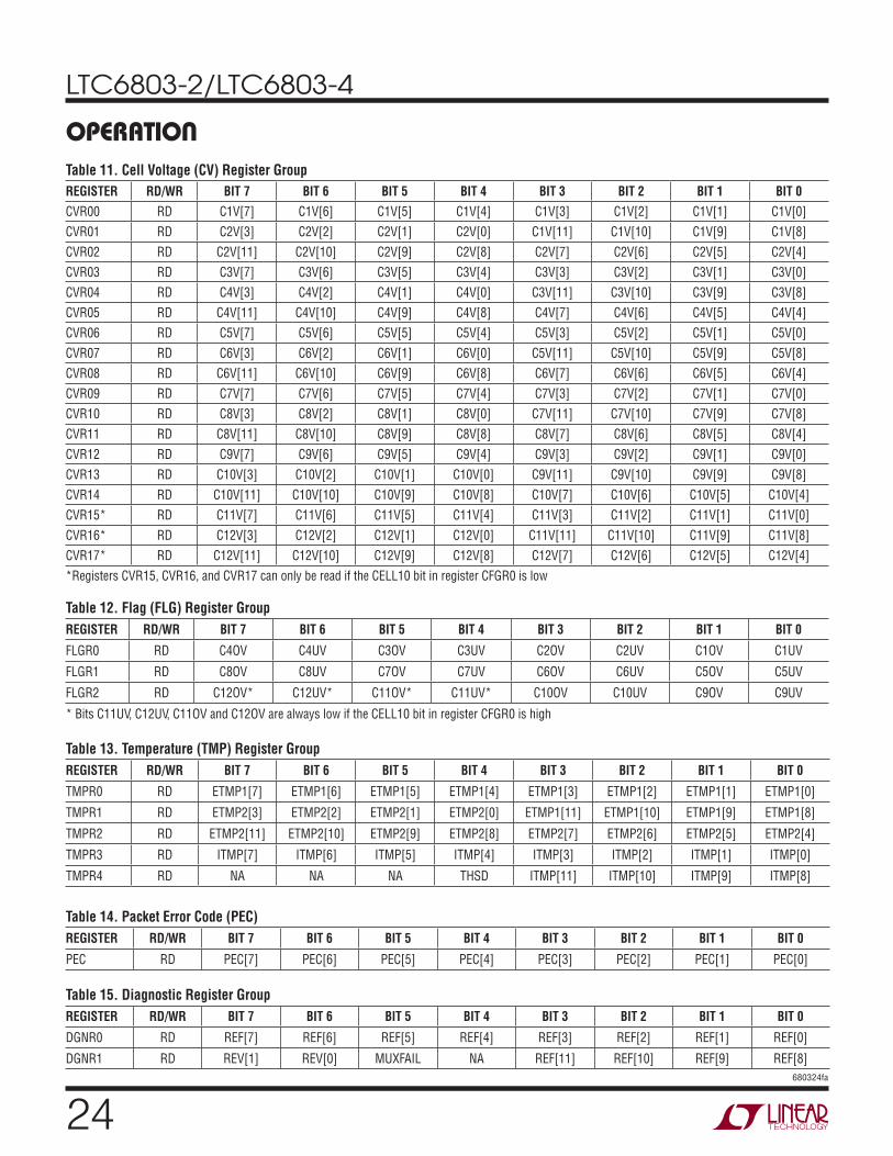
Table 11. Cell Voltage (CV) Register GroupREGISTER RD/WR BIT 7 BIT 6 BIT 5 BIT 4 BIT 3 BIT 2 BIT 1 BIT 0CVR00 RD C1V[7] C1V[6] C1V[5] C1V[4] C1V[3] C1V[2] C1V[1] C1V[0]CVR01 RD C2V[3] C2V[2] C2V[1] C2V[0] C1V[11] C1V[10] C1V[9] C1V[8]CVR02 RD C2V[11] C2V[10] C2V[9] C2V[8] C2V[7] C2V[6] C2V[5] C2V[4]CVR03 RD C3V[7] C3V[6] C3V[5] C3V[4] C3V[3] C3V[2] C3V[1] C3V[0]CVR04 RD C4V[3] C4V[2] C4V[1] C4V[0] C3V[11] C3V[10] C3V[9] C3V[8]CVR05 RD C4V[11] C4V[10] C4V[9] C4V[8] C4V[7] C4V[6] C4V[5] C4V[4]CVR06 RD C5V[7] C5V[6] C5V[5] C5V[4] C5V[3] C5V[2] C5V[1] C5V[0]CVR07 RD C6V[3] C6V[2] C6V[1] C6V[0] C5V[11] C5V[10] C5V[9] C5V[8]CVR08 RD C6V[11] C6V[10] C6V[9] C6V[8] C6V[7] C6V[6] C6V[5] C6V[4]CVR09 RD C7V[7] C7V[6] C7V[5] C7V[4] C7V[3] C7V[2] C7V[1] C7V[0]CVR10 RD C8V[3] C8V[2] C8V[1] C8V[0] C7V[11] C7V[10] C7V[9] C7V[8]CVR11 RD C8V[11] C8V[10] C8V[9] C8V[8] C8V[7] C8V[6] C8V[5] C8V[4]CVR12 RD C9V[7] C9V[6] C9V[5] C9V[4] C9V[3] C9V[2] C9V[1] C9V[0]CVR13 RD C10V[3] C10V[2] C10V[1] C10V[0] C9V[11] C9V[10] C9V[9] C9V[8]CVR14 RD C10V[11] C10V[10] C10V[9] C10V[8] C10V[7] C10V[6] C10V[5] C10V[4]CVR15* RD C11V[7] C11V[6] C11V[5] C11V[4] C11V[3] C11V[2] C11V[1] C11V[0]CVR16* RD C12V[3] C12V[2] C12V[1] C12V[0] C11V[11] C11V[10] C11V[9] C11V[8]CVR17* RD C12V[11] C12V[10] C12V[9] C12V[8] C12V[7] C12V[6] C12V[5] C12V[4]*Registers CVR15, CVR16, and CVR17 can only be read if the CELL10 bit in register CFGR0 is low
OPERATION
Table 12. Flag (FLG) Register GroupREGISTER RD/WR BIT 7 BIT 6 BIT 5 BIT 4 BIT 3 BIT 2 BIT 1 BIT 0
FLGR0 RD C4OV C4UV C3OV C3UV C2OV C2UV C1OV C1UV
FLGR1 RD C8OV C8UV C7OV C7UV C6OV C6UV C5OV C5UV
FLGR2 RD C12OV* C12UV* C11OV* C11UV* C10OV C10UV C9OV C9UV
* Bits C11UV, C12UV, C11OV and C12OV are always low if the CELL10 bit in register CFGR0 is high
Table 13. Temperature (TMP) Register GroupREGISTER RD/WR BIT 7 BIT 6 BIT 5 BIT 4 BIT 3 BIT 2 BIT 1 BIT 0
TMPR0 RD ETMP1[7] ETMP1[6] ETMP1[5] ETMP1[4] ETMP1[3] ETMP1[2] ETMP1[1] ETMP1[0]
TMPR1 RD ETMP2[3] ETMP2[2] ETMP2[1] ETMP2[0] ETMP1[11] ETMP1[10] ETMP1[9] ETMP1[8]
TMPR2 RD ETMP2[11] ETMP2[10] ETMP2[9] ETMP2[8] ETMP2[7] ETMP2[6] ETMP2[5] ETMP2[4]
TMPR3 RD ITMP[7] ITMP[6] ITMP[5] ITMP[4] ITMP[3] ITMP[2] ITMP[1] ITMP[0]
TMPR4 RD NA NA NA THSD ITMP[11] ITMP[10] ITMP[9] ITMP[8]
Table 14. Packet Error Code (PEC)REGISTER RD/WR BIT 7 BIT 6 BIT 5 BIT 4 BIT 3 BIT 2 BIT 1 BIT 0
PEC RD PEC[7] PEC[6] PEC[5] PEC[4] PEC[3] PEC[2] PEC[1] PEC[0]
Table 15. Diagnostic Register GroupREGISTER RD/WR BIT 7 BIT 6 BIT 5 BIT 4 BIT 3 BIT 2 BIT 1 BIT 0
DGNR0 RD REF[7] REF[6] REF[5] REF[4] REF[3] REF[2] REF[1] REF[0]
DGNR1 RD REV[1] REV[0] MUXFAIL NA REF[11] REF[10] REF[9] REF[8]
LTC6803-2/LTC6803-4
25680324fa
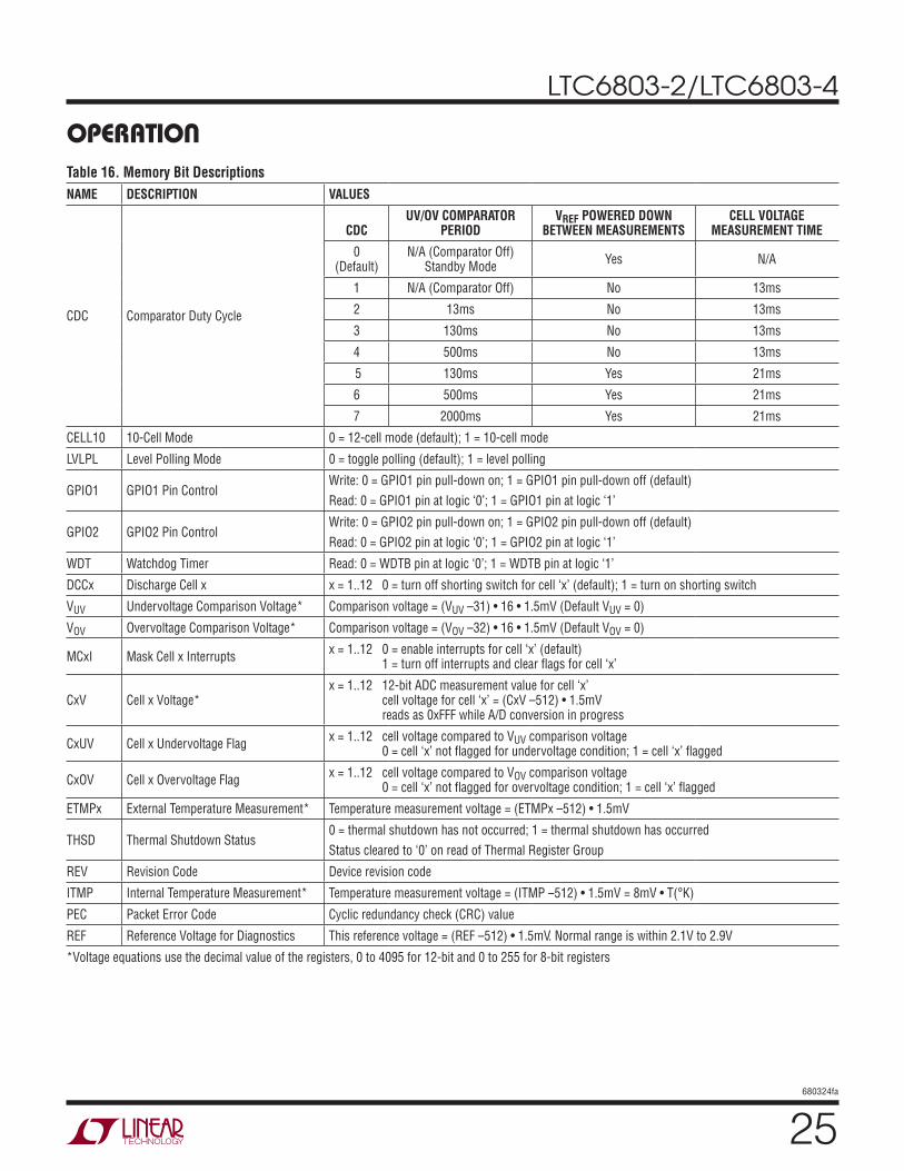
OPERATIONTable 16. Memory Bit DescriptionsNAME DESCRIPTION VALUES
CDC Comparator Duty Cycle
CDCUV/OV COMPARATOR
PERIODVREF POWERED DOWN
BETWEEN MEASUREMENTSCELL VOLTAGE
MEASUREMENT TIME
0 (Default)
N/A (Comparator Off) Standby Mode Yes N/A
1 N/A (Comparator Off) No 13ms
2 13ms No 13ms
3 130ms No 13ms
4 500ms No 13ms
5 130ms Yes 21ms
6 500ms Yes 21ms
7 2000ms Yes 21ms
CELL10 10-Cell Mode 0 = 12-cell mode (default); 1 = 10-cell mode
LVLPL Level Polling Mode 0 = toggle polling (default); 1 = level polling
GPIO1 GPIO1 Pin ControlWrite: 0 = GPIO1 pin pull-down on; 1 = GPIO1 pin pull-down off (default)Read: 0 = GPIO1 pin at logic ‘0’; 1 = GPIO1 pin at logic ‘1’
GPIO2 GPIO2 Pin ControlWrite: 0 = GPIO2 pin pull-down on; 1 = GPIO2 pin pull-down off (default)Read: 0 = GPIO2 pin at logic ‘0’; 1 = GPIO2 pin at logic ‘1’
WDT Watchdog Timer Read: 0 = WDTB pin at logic ‘0’; 1 = WDTB pin at logic ‘1’
DCCx Discharge Cell x x = 1..12 0 = turn off shorting switch for cell ‘x’ (default); 1 = turn on shorting switch
VUV Undervoltage Comparison Voltage* Comparison voltage = (VUV –31) • 16 • 1.5mV (Default VUV = 0)
VOV Overvoltage Comparison Voltage* Comparison voltage = (VOV –32) • 16 • 1.5mV (Default VOV = 0)
MCxI Mask Cell x Interrupts x = 1..12 0 = enable interrupts for cell ‘x’ (default) 1 = turn off interrupts and clear flags for cell ‘x’
CxV Cell x Voltage*x = 1..12 12-bit ADC measurement value for cell ‘x’ cell voltage for cell ‘x’ = (CxV –512) • 1.5mV reads as 0xFFF while A/D conversion in progress
CxUV Cell x Undervoltage Flag x = 1..12 cell voltage compared to VUV comparison voltage 0 = cell ‘x’ not flagged for undervoltage condition; 1 = cell ‘x’ flagged
CxOV Cell x Overvoltage Flag x = 1..12 cell voltage compared to VOV comparison voltage 0 = cell ‘x’ not flagged for overvoltage condition; 1 = cell ‘x’ flagged
ETMPx External Temperature Measurement* Temperature measurement voltage = (ETMPx –512) • 1.5mV
THSD Thermal Shutdown Status0 = thermal shutdown has not occurred; 1 = thermal shutdown has occurredStatus cleared to ‘0’ on read of Thermal Register Group
REV Revision Code Device revision code
ITMP Internal Temperature Measurement* Temperature measurement voltage = (ITMP –512) • 1.5mV = 8mV • T(°K)
PEC Packet Error Code Cyclic redundancy check (CRC) value
REF Reference Voltage for Diagnostics This reference voltage = (REF –512) • 1.5mV. Normal range is within 2.1V to 2.9V
*Voltage equations use the decimal value of the registers, 0 to 4095 for 12-bit and 0 to 255 for 8-bit registers
LTC6803-2/LTC6803-4
26680324fa
SERIAL COMMAND EXAMPLES
LTC6803-2/LTC6803-4 (Addressable Configuration)
Examples below use a configuration of three stacked devices: bottom (B), middle (M), and top (T)
Write Configuration Registers (Figure 7) (Broadcast Write)
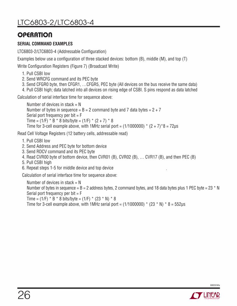
1. Pull CSBI low2. Send WRCFG command and its PEC byte3. Send CFGR0 byte, then CFGR1, …CFGR5, PEC byte (All devices on the bus receive the same data)4. Pull CSBI high; data latched into all devices on rising edge of CSBI. S pins respond as data latched
Calculation of serial interface time for sequence above:
Number of devices in stack = NNumber of bytes in sequence = B = 2 command byte and 7 data bytes = 2 + 7Serial port frequency per bit = FTime = (1/F) * B * 8 bits/byte = (1/F) * (2 + 7) * 8Time for 3-cell example above, with 1MHz serial port = (1/1000000) * (2 + 7)*8 = 72µs
Read Cell Voltage Registers (12 battery cells, addressable read)
1. Pull CSBI low2. Send Address and PEC byte for bottom device3. Send RDCV command and its PEC byte4. Read CVR00 byte of bottom device, then CVR01 (B), CVR02 (B), … CVR17 (B), and then PEC (B)5. Pull CSBI high6. Repeat steps 1-5 for middle device and top device
Calculation of serial interface time for sequence above:
Number of devices in stack = NNumber of bytes in sequence = B = 2 address bytes, 2 command bytes, and 18 data bytes plus 1 PEC byte = 23 * NSerial port frequency per bit = FTime = (1/F) * B * 8 bits/byte = (1/F) * (23 * N) * 8Time for 3-cell example above, with 1MHz serial port = (1/1000000) * (23 * N) * 8 = 552µs
OPERATION
LTC6803-2/LTC6803-4
27680324fa
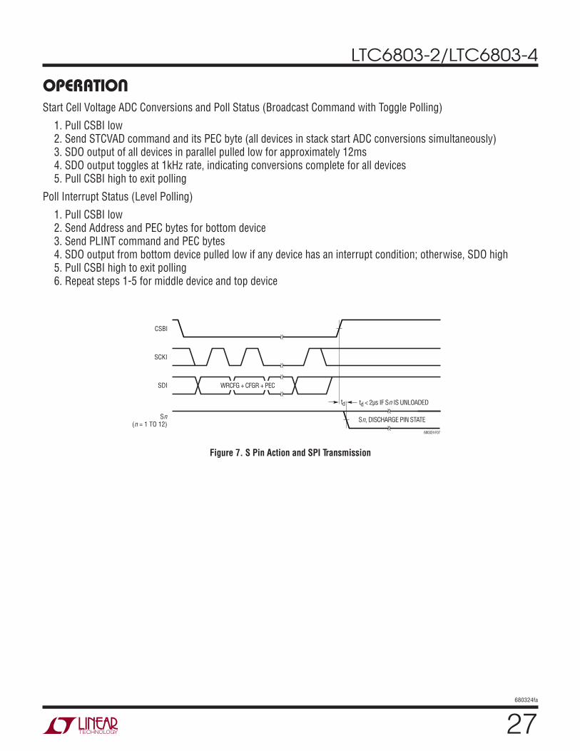
OPERATIONStart Cell Voltage ADC Conversions and Poll Status (Broadcast Command with Toggle Polling)
1. Pull CSBI low2. Send STCVAD command and its PEC byte (all devices in stack start ADC conversions simultaneously)3. SDO output of all devices in parallel pulled low for approximately 12ms 4. SDO output toggles at 1kHz rate, indicating conversions complete for all devices5. Pull CSBI high to exit polling
Poll Interrupt Status (Level Polling)
1. Pull CSBI low2. Send Address and PEC bytes for bottom device3. Send PLINT command and PEC bytes4. SDO output from bottom device pulled low if any device has an interrupt condition; otherwise, SDO high5. Pull CSBI high to exit polling6. Repeat steps 1-5 for middle device and top device
CSBI
SCKI
SDI
Sn(n = 1 TO 12)
Sn, DISCHARGE PIN STATE
td < 2µs IF Sn IS UNLOADEDtd
680324 F07
WRCFG + CFGR + PEC
Figure 7. S Pin Action and SPI Transmission
LTC6803-2/LTC6803-4
28680324fa
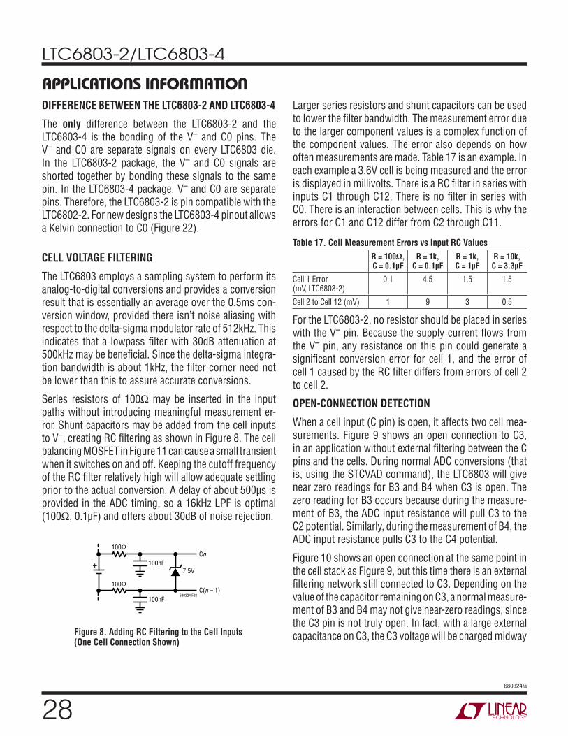
APPLICATIONS INFORMATIONDIFFERENCE BETWEEN THE LTC6803-2 AND LTC6803-4
The only difference between the LTC6803-2 and the LTC6803-4 is the bonding of the V– and C0 pins. The V– and C0 are separate signals on every LTC6803 die. In the LTC6803-2 package, the V– and C0 signals are shorted together by bonding these signals to the same pin. In the LTC6803-4 package, V– and C0 are separate pins. Therefore, the LTC6803-2 is pin compatible with the LTC6802-2. For new designs the LTC6803-4 pinout allows a Kelvin connection to C0 (Figure 22).
CELL VOLTAGE FILTERING
The LTC6803 employs a sampling system to perform its analog-to-digital conversions and provides a conversion result that is essentially an average over the 0.5ms con-version window, provided there isn’t noise aliasing with respect to the delta-sigma modulator rate of 512kHz. This indicates that a lowpass filter with 30dB attenuation at 500kHz may be beneficial. Since the delta-sigma integra-tion bandwidth is about 1kHz, the filter corner need not be lower than this to assure accurate conversions.
Series resistors of 100Ω may be inserted in the input paths without introducing meaningful measurement er-ror. Shunt capacitors may be added from the cell inputs to V–, creating RC filtering as shown in Figure 8. The cell balancing MOSFET in Figure 11 can cause a small transient when it switches on and off. Keeping the cutoff frequency of the RC filter relatively high will allow adequate settling prior to the actual conversion. A delay of about 500µs is provided in the ADC timing, so a 16kHz LPF is optimal (100Ω, 0.1µF) and offers about 30dB of noise rejection.
Larger series resistors and shunt capacitors can be used to lower the filter bandwidth. The measurement error due to the larger component values is a complex function of the component values. The error also depends on how often measurements are made. Table 17 is an example. In each example a 3.6V cell is being measured and the error is displayed in millivolts. There is a RC filter in series with inputs C1 through C12. There is no filter in series with C0. There is an interaction between cells. This is why the errors for C1 and C12 differ from C2 through C11.
Table 17. Cell Measurement Errors vs Input RC ValuesR = 100Ω, C = 0.1µF
R = 1k, C = 0.1µF
R = 1k, C = 1µF
R = 10k, C = 3.3µF
Cell 1 Error (mV, LTC6803-2)
0.1 4.5 1.5 1.5
Cell 2 to Cell 12 (mV) 1 9 3 0.5
For the LTC6803-2, no resistor should be placed in series with the V– pin. Because the supply current flows from the V– pin, any resistance on this pin could generate a significant conversion error for cell 1, and the error of cell 1 caused by the RC filter differs from errors of cell 2 to cell 2.
OPEN-CONNECTION DETECTION
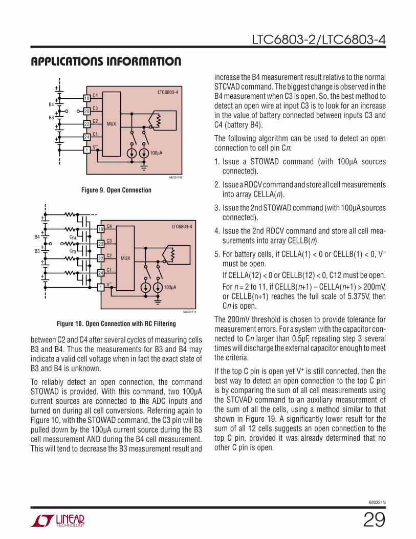
When a cell input (C pin) is open, it affects two cell mea-surements. Figure 9 shows an open connection to C3, in an application without external filtering between the C pins and the cells. During normal ADC conversions (that is, using the STCVAD command), the LTC6803 will give near zero readings for B3 and B4 when C3 is open. The zero reading for B3 occurs because during the measure-ment of B3, the ADC input resistance will pull C3 to the C2 potential. Similarly, during the measurement of B4, the ADC input resistance pulls C3 to the C4 potential.
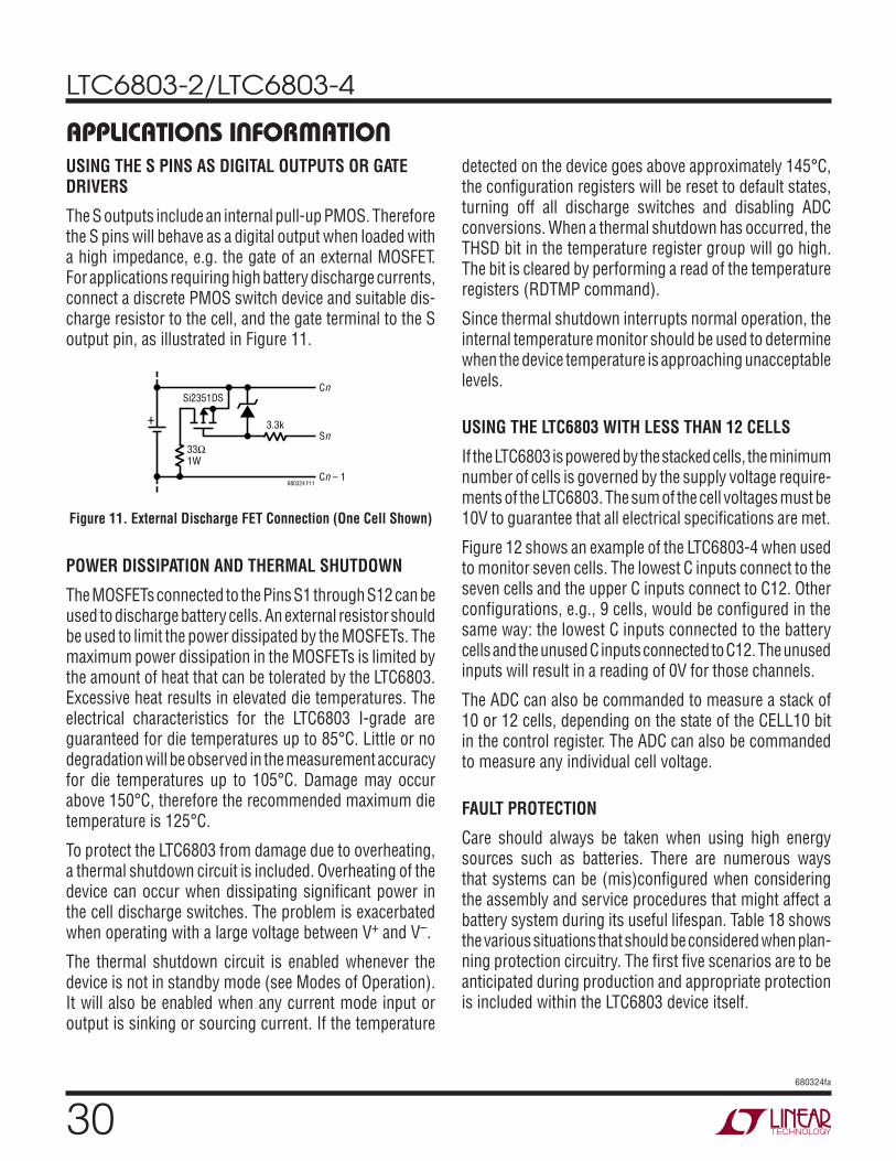
Figure 10 shows an open connection at the same point in the cell stack as Figure 9, but this time there is an external filtering network still connected to C3. Depending on the value of the capacitor remaining on C3, a normal measure-ment of B3 and B4 may not give near-zero readings, since the C3 pin is not truly open. In fact, with a large external capacitance on C3, the C3 voltage will be charged midway Figure 8. Adding RC Filtering to the Cell Inputs
(One Cell Connection Shown)
+ 100nF
100nF680324 F08
7.5V
Cn
C(n – 1)
100Ω
100Ω
LTC6803-2/LTC6803-4
29680324fa
APPLICATIONS INFORMATION
Figure 9. Open Connection
Figure 10. Open Connection with RC Filtering
between C2 and C4 after several cycles of measuring cells B3 and B4. Thus the measurements for B3 and B4 may indicate a valid cell voltage when in fact the exact state of B3 and B4 is unknown.
To reliably detect an open connection, the command STOWAD is provided. With this command, two 100µA current sources are connected to the ADC inputs and turned on during all cell conversions. Referring again to Figure 10, with the STOWAD command, the C3 pin will be pulled down by the 100µA current source during the B3 cell measurement AND during the B4 cell measurement. This will tend to decrease the B3 measurement result and
increase the B4 measurement result relative to the normal STCVAD command. The biggest change is observed in the B4 measurement when C3 is open. So, the best method to detect an open wire at input C3 is to look for an increase in the value of battery connected between inputs C3 and C4 (battery B4).
The following algorithm can be used to detect an open connection to cell pin Cn:
1. Issue a STOWAD command (with 100µA sources connected).
2. Issue a RDCV command and store all cell measurements into array CELLA(n).
3. Issue the 2nd STOWAD command (with 100µA sources connected).
4. Issue the 2nd RDCV command and store all cell mea-surements into array CELLB(n).
5. For battery cells, if CELLA(1) < 0 or CELLB(1) < 0, V– must be open.
If CELLA(12) < 0 or CELLB(12) < 0, C12 must be open. For n = 2 to 11, if CELLB(n+1) – CELLA(n+1) > 200mV,
or CELLB(n+1) reaches the full scale of 5.375V, then Cn is open.
The 200mV threshold is chosen to provide tolerance for measurement errors. For a system with the capacitor con-nected to Cn larger than 0.5µF, repeating step 3 several times will discharge the external capacitor enough to meet the criteria.
If the top C pin is open yet V+ is still connected, then the best way to detect an open connection to the top C pin is by comparing the sum of all cell measurements using the STCVAD command to an auxiliary measurement of the sum of all the cells, using a method similar to that shown in Figure 19. A significantly lower result for the sum of all 12 cells suggests an open connection to the top C pin, provided it was already determined that no other C pin is open.
+
+
+
+
+
100µA
MUXC222
C320
C4
B4
B3
680324 F09
LTC6803-418
V–1
C124
+
+
+
+
+
100µA
MUXC222
C320
C4
B4 CF4
CF3B3
680324 F10
LTC6803-418
V–1
C124
LTC6803-2/LTC6803-4
30680324fa
USING THE S PINS AS DIGITAL OUTPUTS OR GATE DRIVERS
The S outputs include an internal pull-up PMOS. Therefore the S pins will behave as a digital output when loaded with a high impedance, e.g. the gate of an external MOSFET. For applications requiring high battery discharge currents, connect a discrete PMOS switch device and suitable dis-charge resistor to the cell, and the gate terminal to the S output pin, as illustrated in Figure 11.
detected on the device goes above approximately 145°C, the configuration registers will be reset to default states, turning off all discharge switches and disabling ADC conversions. When a thermal shutdown has occurred, the THSD bit in the temperature register group will go high. The bit is cleared by performing a read of the temperature registers (RDTMP command).
Since thermal shutdown interrupts normal operation, the internal temperature monitor should be used to determine when the device temperature is approaching unacceptable levels.
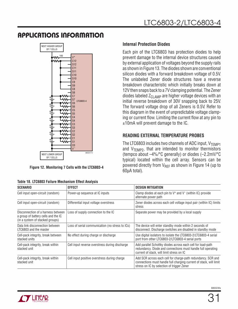
USING THE LTC6803 WITH LESS THAN 12 CELLS
If the LTC6803 is powered by the stacked cells, the minimum number of cells is governed by the supply voltage require-ments of the LTC6803. The sum of the cell voltages must be 10V to guarantee that all electrical specifications are met.
Figure 12 shows an example of the LTC6803-4 when used to monitor seven cells. The lowest C inputs connect to the seven cells and the upper C inputs connect to C12. Other configurations, e.g., 9 cells, would be configured in the same way: the lowest C inputs connected to the battery cells and the unused C inputs connected to C12. The unused inputs will result in a reading of 0V for those channels.
The ADC can also be commanded to measure a stack of 10 or 12 cells, depending on the state of the CELL10 bit in the control register. The ADC can also be commanded to measure any individual cell voltage.
FAULT PROTECTION
Care should always be taken when using high energy sources such as batteries. There are numerous ways that systems can be (mis)configured when considering the assembly and service procedures that might affect a battery system during its useful lifespan. Table 18 shows the various situations that should be considered when plan-ning protection circuitry. The first five scenarios are to be anticipated during production and appropriate protection is included within the LTC6803 device itself.
APPLICATIONS INFORMATION
Figure 11. External Discharge FET Connection (One Cell Shown)
+
680324 F11
Cn
Cn – 1
Sn3.3k
33Ω1W
Si2351DS
POWER DISSIPATION AND THERMAL SHUTDOWN
The MOSFETs connected to the Pins S1 through S12 can be used to discharge battery cells. An external resistor should be used to limit the power dissipated by the MOSFETs. The maximum power dissipation in the MOSFETs is limited by the amount of heat that can be tolerated by the LTC6803. Excessive heat results in elevated die temperatures. The electrical characteristics for the LTC6803 I-grade are guaranteed for die temperatures up to 85°C. Little or no degradation will be observed in the measurement accuracy for die temperatures up to 105°C. Damage may occur above 150°C, therefore the recommended maximum die temperature is 125°C.
To protect the LTC6803 from damage due to overheating, a thermal shutdown circuit is included. Overheating of the device can occur when dissipating significant power in the cell discharge switches. The problem is exacerbated when operating with a large voltage between V+ and V–.
The thermal shutdown circuit is enabled whenever the device is not in standby mode (see Modes of Operation). It will also be enabled when any current mode input or output is sinking or sourcing current. If the temperature
LTC6803-2/LTC6803-4
31680324fa
APPLICATIONS INFORMATION
Table 18. LTC6803 Failure Mechanism Effect AnalysisSCENARIO EFFECT DESIGN MITIGATION
Cell input open-circuit (random) Power-up sequence at IC inputs Clamp diodes at each pin to V+ and V– (within IC) provide alternate power path
Cell input open-circuit (random) Differential input voltage overstress Zener diodes across each cell voltage input pair (within IC) limits stress
Disconnection of a harness between a group of battery cells and the IC (in a system of stacked groups)
Loss of supply connection to the IC Separate power may be provided by a local supply
Data link disconnection between LTC6803 and the master
Loss of serial communication (no stress to ICs) The device will enter standby mode within 2 seconds of disconnect. Discharge switches are disabled in standby mode
Cell-pack integrity, break between stacked units
No effect during charge or discharge Use digital isolators to isolate the LTC6803-2/LTC6803-4 serial port from other LTC6803-2/LTC6803-4 serial ports
Cell-pack integrity, break within stacked unit
Cell input reverse overstress during discharge Add parallel Schottky diodes across each cell for load-path redundancy. Diode and connections must handle full operating current of stack, will limit stress on IC
Cell-pack integrity, break within stacked unit
Cell input positive overstress during charge Add SCR across each cell for charge-path redundancy. SCR and connections must handle full charging current of stack, will limit stress on IC by selection of trigger Zener
Internal Protection Diodes
Each pin of the LTC6803 has protection diodes to help prevent damage to the internal device structures caused by external application of voltages beyond the supply rails as shown in Figure 13. The diodes shown are conventional silicon diodes with a forward breakdown voltage of 0.5V. The unlabeled Zener diode structures have a reverse breakdown characteristic which initially breaks down at 12V then snaps back to a 7V clamping potential. The Zener diodes labeled ZCLAMP are higher voltage devices with an initial reverse breakdown of 30V snapping back to 25V. The forward voltage drop of all Zeners is 0.5V. Refer to this diagram in the event of unpredictable voltage clamp-ing or current flow. Limiting the current flow at any pin to ±10mA will prevent damage to the IC.
READING EXTERNAL TEMPERATURE PROBES
The LTC6803 includes two channels of ADC input, VTEMP1 and VTEMP2, that are intended to monitor thermistors (tempco about –4%/°C generally) or diodes (–2.2mV/°C typical) located within the cell array. Sensors can be powered directly from VREF as shown in Figure 14 (up to 60µA total).
+
+
+
+
+
+
+
V+
C12S12C11S11C10S10C9S9C8S8C7S7C6S6C5S5C4S4C3S3C2S2C1S1C0V–
LTC6803-4
100
NEXT HIGHER GROUPOF 7 CELLS
NEXT LOWER GROUPOF 7 CELLS
680324 F12
Figure 12. Monitoring 7 Cells with the LTC6803-4
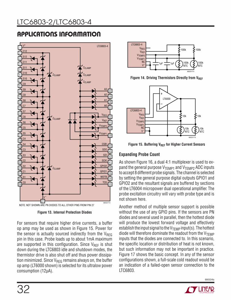
LTC6803-2/LTC6803-4
32680324fa
APPLICATIONS INFORMATION
For sensors that require higher drive currents, a buffer op amp may be used as shown in Figure 15. Power for the sensor is actually sourced indirectly from the VREG pin in this case. Probe loads up to about 1mA maximum are supported in this configuration. Since VREF is shut down during the LTC6803 idle and shutdown modes, the thermistor drive is also shut off and thus power dissipa-tion minimized. Since VREG remains always on, the buffer op amp (LT6000 shown) is selected for its ultralow power consumption (12µA).
Figure 13. Internal Protection Diodes
Expanding Probe Count
As shown Figure 16, a dual 4:1 multiplexer is used to ex-pand the general purpose VTEMP1 and VTEMP2 ADC inputs to accept 8 different probe signals. The channel is selected by setting the general purpose digital outputs GPIO1 and GPIO2 and the resultant signals are buffered by sections of the LT6004 micropower dual operational amplifier. The probe excitation circuitry will vary with probe type and is not shown here.
Another method of multiple sensor support is possible without the use of any GPIO pins. If the sensors are PN diodes and several used in parallel, then the hottest diode will produce the lowest forward voltage and effectively establish the input signal to the VTEMP input(s). The hottest diode will therefore dominate the readout from the VTEMP inputs that the diodes are connected to. In this scenario, the specific location or distribution of heat is not known, but such information may not be important in practice. Figure 17 shows the basic concept. In any of the sensor configurations shown, a full-scale cold readout would be an indication of a failed-open sensor connection to the LTC6803.
Figure 14. Driving Thermistors Directly from VREF
Figure 15. Buffering VREF for Higher Current Sensors
3S12
2C12
1V+
4C11
5S11
6C10 ZCLAMP
LTC6803-4
ZCLAMP
ZCLAMP
ZCLAMP
ZCLAMP
ZCLAMP
7S10
8C9
9S9
10C8
11S8
12C7
13S7
14C6
15S6
16C5
17S5
18C4
19S4
20C3
21S3
22C2
23S2
24C1
25S1
26
27
C0
NOTE: NOT SHOWN ARE PN DIODES TO ALL OTHER PINS FROM PIN 27
V–
44CSBI
43SDO
42SDI
41SCKI
40A3
39A2
38A1
37A0
32VREG
VREF
VTEMP2
VTEMP1
31
30
29
36GPIO2
35GPIO1
34WDTB
33TOS
680324 F13
VREGVREF
VTEMP2VTEMP1
NCV–
LTC6803-4
1µF
680324 F14
1µF 100kNTC
100k 100k
100kNTC
VREGVREF
VTEMP2VTEMP1
NCV–
LTC6803-4
680324 F15
10kNTC
10k 10k
10kNTC
–
+LT6000
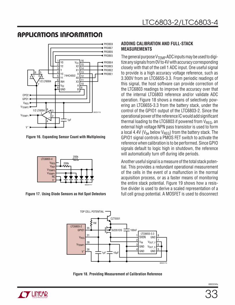
LTC6803-2/LTC6803-4
33680324fa
APPLICATIONS INFORMATIONADDING CALIBRATION AND FULL-STACK MEASUREMENTS
The general purpose VTEMP ADC inputs may be used to digi-tize any signals from 0V to 4V with accuracy corresponding closely with that of the cell 1 ADC input. One useful signal to provide is a high accuracy voltage reference, such as 3.300V from an LTC6655-3.3. From periodic readings of this signal, the host software can provide correction of the LTC6803 readings to improve the accuracy over that of the internal LTC6803 reference and/or validate ADC operation. Figure 18 shows a means of selectively pow-ering an LTC6655-3.3 from the battery stack, under the control of the GPIO1 output of the LTC6803-2. Since the operational power of the reference IC would add significant thermal loading to the LTC6803 if powered from VREG, an external high voltage NPN pass transistor is used to form a local 4.4V (Vbe below VREG) from the battery stack. The GPIO1 signal controls a PMOS FET switch to activate the reference when calibration is to be performed. Since GPIO signals default to logic high in shutdown, the reference will automatically turn off during idle periods.
Another useful signal is a measure of the total stack poten-tial. This provides a redundant operational measurement of the cells in the event of a malfunction in the normal acquisition process, or as a faster means of monitoring the entire stack potential. Figure 19 shows how a resis-tive divider is used to derive a scaled representation of a full cell group potential. A MOSFET is used to disconnect
Figure 16. Expanding Sensor Count with Multiplexing
Figure 17. Using Diode Sensors as Hot Spot Detectors
6
4 8
7
18 3
21µF
680324 F16
4
1/2 LT6004
1/2 LT6004 +–
+–
12345678
161514131211109
Y0Y2YY3Y1INHVEEGND
PROBE8PROBE7PROBE6PROBE5
PROBE4PROBE3PROBE2PROBE1
CPO2GPO1VREG
VTEMP2
VTEMP1
V–
VCCX2X1X
X0X3AB
74HC40525
VREGVREF
VTEMP2VTEMP1
NCV–
LTC6803-4
200k
680324 F17
200k
GPIO135
VREG31
VTEMP128
V– 26
1M
TOP CELL POTENTIAL
Si2351DS 100nFLTC6803-2
SHDN
VIN
GND
GND
GND
VOUT_F
VOUT_S
GND
1
2
3
4
8
7
6
51µF 10µF
680324 F18
LTC6655-3.3
CZT5551
Figure 18. Providing Measurement of Calibration Reference
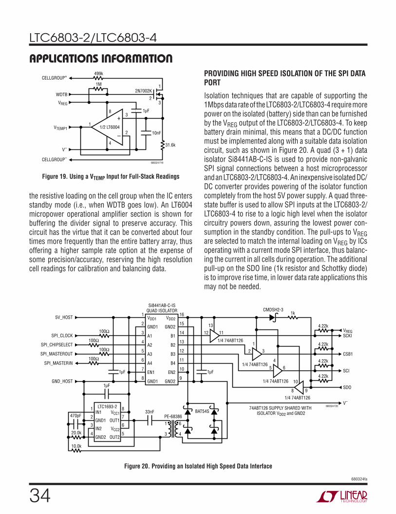
LTC6803-2/LTC6803-4
34680324fa
APPLICATIONS INFORMATION
Figure 19. Using a VTEMP Input for Full-Stack Readings
the resistive loading on the cell group when the IC enters standby mode (i.e., when WDTB goes low). An LT6004 micropower operational amplifier section is shown for buffering the divider signal to preserve accuracy. This circuit has the virtue that it can be converted about four times more frequently than the entire battery array, thus offering a higher sample rate option at the expense of some precision/accuracy, reserving the high resolution cell readings for calibration and balancing data.
Figure 20. Providing an Isolated High Speed Data Interface
–
+1/2 LT6004VTEMP1
VREG
WDTB
V–
CELLGROUP–
CELLGROUP+
1
3
3
1
2
2N7002K
1µF
10nF
680324 F19
31.6k
2
4
8
499k
1M
PROVIDING HIGH SPEED ISOLATION OF THE SPI DATA PORT
Isolation techniques that are capable of supporting the 1Mbps data rate of the LTC6803-2/LTC6803-4 require more power on the isolated (battery) side than can be furnished by the VREG output of the LTC6803-2/LTC6803-4. To keep battery drain minimal, this means that a DC/DC function must be implemented along with a suitable data isolation circuit, such as shown in Figure 20. A quad (3 + 1) data isolator Si8441AB-C-IS is used to provide non-galvanic SPI signal connections between a host microprocessor and an LTC6803-2/LTC6803-4. An inexpensive isolated DC/DC converter provides powering of the isolator function completely from the host 5V power supply. A quad three-state buffer is used to allow SPI inputs at the LTC6803-2/LTC6803-4 to rise to a logic high level when the isolator circuitry powers down, assuring the lowest power con-sumption in the standby condition. The pull-ups to VREG are selected to match the internal loading on VREG by ICs operating with a current mode SPI interface, thus balanc-ing the current in all cells during operation. The additional pull-up on the SDO line (1k resistor and Schottky diode) is to improve rise time, in lower data rate applications this may not be needed.
VDD1
GND1
A1
A2
A3
A4
EN1
GND1
VDD2
GND2
B1
B2
B3
B4
EN2
GND2
1
2
3
4
5
6
7
8
16
15
14
13
12
11
10
9
Si8441AB-C-ISQUAD ISOLATOR 1k
4.22kVREG
SDO
SCKI
CSB1
SCI
V–
1µF1µF
BAT54S
CMDSH2-3
6PE-68386
33nF
• •
4
1
3
12
13
1/4 74ABT126
11
2
1
1/4 74ABT126
3
5
4
1/4 74ABT126
6
8
10
1/4 74ABT126
74ABT126 SUPPLY SHARED WITH ISOLATOR VDD2 and GND2
9
4.22k
4.22k
4.22k
680324 F20
1µF
470pFIN1
GND1
IN2
GND2
8
7
6
5
1
2
3
4
VCC1
OUT1
VCC2
OUT2
LTC1693-2
20.0k
100Ω
5V_HOST
100Ω
100Ω
100Ω
10.0k
SPI_CLOCK
SPI_CHIPSELECT
SPI_MASTEROUT
SPI_MASTERIN
GND_HOST
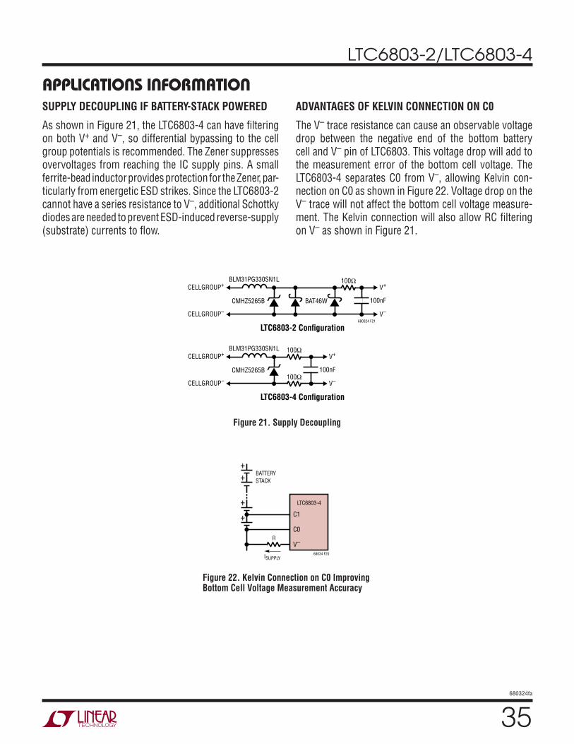
LTC6803-2/LTC6803-4
35680324fa
APPLICATIONS INFORMATIONSUPPLY DECOUPLING IF BATTERY-STACK POWERED
As shown in Figure 21, the LTC6803-4 can have filtering on both V+ and V–, so differential bypassing to the cell group potentials is recommended. The Zener suppresses overvoltages from reaching the IC supply pins. A small ferrite-bead inductor provides protection for the Zener, par-ticularly from energetic ESD strikes. Since the LTC6803-2 cannot have a series resistance to V–, additional Schottky diodes are needed to prevent ESD-induced reverse-supply (substrate) currents to flow.
ADVANTAGES OF KELVIN CONNECTION ON C0
The V– trace resistance can cause an observable voltage drop between the negative end of the bottom battery cell and V– pin of LTC6803. This voltage drop will add to the measurement error of the bottom cell voltage. The LTC6803-4 separates C0 from V–, allowing Kelvin con-nection on C0 as shown in Figure 22. Voltage drop on the V– trace will not affect the bottom cell voltage measure-ment. The Kelvin connection will also allow RC filtering on V– as shown in Figure 21.
Figure 21. Supply Decoupling
Figure 22. Kelvin Connection on C0 Improving Bottom Cell Voltage Measurement Accuracy
CELLGROUP+
CELLGROUP–
CMHZ5265B BAT46W
100Ω
100nF
V+
V–
BLM31PG330SN1L
LTC6803-2 Configuration
CELLGROUP+
CELLGROUP–
CMHZ5265B
100Ω
100Ω100nF
680324 F21
V+
V–
BLM31PG330SN1L
LTC6803-4 Configuration
ISUPPLY68034 F20
BATTERYSTACK
R
+
+
++
C1
C0
V–
LTC6803-4
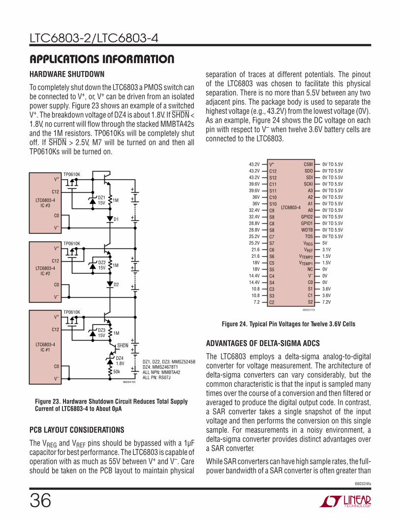
LTC6803-2/LTC6803-4
36680324fa
APPLICATIONS INFORMATIONHARDWARE SHUTDOWN
To completely shut down the LTC6803 a PMOS switch can be connected to V+, or, V+ can be driven from an isolated power supply. Figure 23 shows an example of a switched V+. The breakdown voltage of DZ4 is about 1.8V. If SHDN < 1.8V, no current will flow through the stacked MMBTA42s and the 1M resistors. TP0610Ks will be completely shut off. If SHDN > 2.5V, M7 will be turned on and then all TP0610Ks will be turned on.
separation of traces at different potentials. The pinout of the LTC6803 was chosen to facilitate this physical separation. There is no more than 5.5V between any two adjacent pins. The package body is used to separate the highest voltage (e.g., 43.2V) from the lowest voltage (0V). As an example, Figure 24 shows the DC voltage on each pin with respect to V– when twelve 3.6V battery cells are connected to the LTC6803.
Figure 24. Typical Pin Voltages for Twelve 3.6V Cells
Figure 23. Hardware Shutdown Circuit Reduces Total Supply Current of LTC6803-4 to About 0µA
TP0610K
DZ315V
DZ41.8V DZ1, DZ2, DZ3: MMSZ5245B
DZ4: MMSZ4678T1ALL NPN: MMBTA42ALL PN: RS07J
1M
50k
680324 F23
SHDN
V+
V–
C0
C12
LTC6803-4IC #1
TP0610K
DZ215V 1M
D2
V+
V–
C0
C12
LTC6803-4IC #2
TP0610K
DZ115V 1M
D1
V+
V–
C0
C12
LTC6803-4IC #3
+
++
+
++
+
++
V+
C12S12C11S11C10S10C9S9C8S8C7S7C6S6C5S5C4S4C3S3C2
CSBISDOSDI
SCKIA3A2A1A0
GPIO2GPIO1WDTB
TOSVREGVREF
VTEMP2VTEMP1
NCV–
C0S1C1S2
43.2V43.2V43.2V39.6V39.6V
36V36V
32.4V32.4V28.8V28.8V25.2V25.2V
21.621.618V18V
14.4V14.4V
10.810.87.2
0V TO 5.5V0V TO 5.5V0V TO 5.5V0V TO 5.5V0V TO 5.5V0V TO 5.5V0V TO 5.5V0V TO 5.5V0V TO 5.5V0V TO 5.5V0V TO 5.5V0V TO 5.5V5V3.1V1.5V1.5V0V0V0V3.6V3.6V7.2V
LTC6803-4
680324 F24
PCB LAYOUT CONSIDERATIONS
The VREG and VREF pins should be bypassed with a 1µF capacitor for best performance. The LTC6803 is capable of operation with as much as 55V between V+ and V–. Care should be taken on the PCB layout to maintain physical
ADVANTAGES OF DELTA-SIGMA ADCS
The LTC6803 employs a delta-sigma analog-to-digital converter for voltage measurement. The architecture of delta-sigma converters can vary considerably, but the common characteristic is that the input is sampled many times over the course of a conversion and then filtered or averaged to produce the digital output code. In contrast, a SAR converter takes a single snapshot of the input voltage and then performs the conversion on this single sample. For measurements in a noisy environment, a delta-sigma converter provides distinct advantages over a SAR converter.
While SAR converters can have high sample rates, the full-power bandwidth of a SAR converter is often greater than
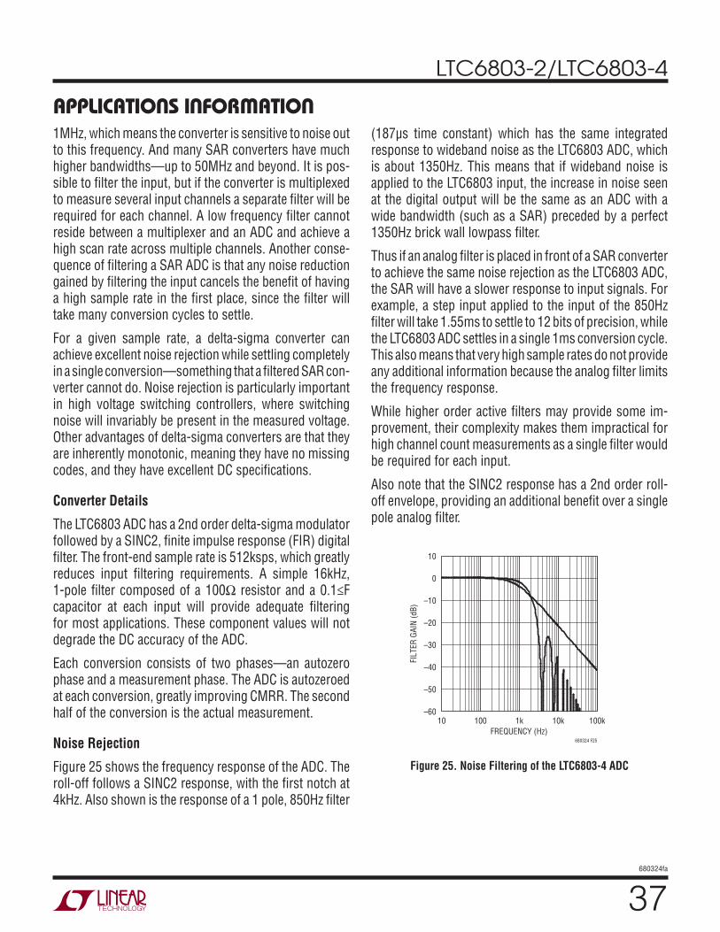
LTC6803-2/LTC6803-4
37680324fa
APPLICATIONS INFORMATION1MHz, which means the converter is sensitive to noise out to this frequency. And many SAR converters have much higher bandwidths—up to 50MHz and beyond. It is pos-sible to filter the input, but if the converter is multiplexed to measure several input channels a separate filter will be required for each channel. A low frequency filter cannot reside between a multiplexer and an ADC and achieve a high scan rate across multiple channels. Another conse-quence of filtering a SAR ADC is that any noise reduction gained by filtering the input cancels the benefit of having a high sample rate in the first place, since the filter will take many conversion cycles to settle.
For a given sample rate, a delta-sigma converter can achieve excellent noise rejection while settling completely in a single conversion—something that a filtered SAR con-verter cannot do. Noise rejection is particularly important in high voltage switching controllers, where switching noise will invariably be present in the measured voltage. Other advantages of delta-sigma converters are that they are inherently monotonic, meaning they have no missing codes, and they have excellent DC specifications.
Converter Details
The LTC6803 ADC has a 2nd order delta-sigma modulator followed by a SINC2, finite impulse response (FIR) digital filter. The front-end sample rate is 512ksps, which greatly reduces input filtering requirements. A simple 16kHz, 1-pole filter composed of a 100Ω resistor and a 0.1≤F capacitor at each input will provide adequate filtering for most applications. These component values will not degrade the DC accuracy of the ADC.
Each conversion consists of two phases—an autozero phase and a measurement phase. The ADC is autozeroed at each conversion, greatly improving CMRR. The second half of the conversion is the actual measurement.
Noise Rejection
Figure 25 shows the frequency response of the ADC. The roll-off follows a SINC2 response, with the first notch at 4kHz. Also shown is the response of a 1 pole, 850Hz filter
(187µs time constant) which has the same integrated response to wideband noise as the LTC6803 ADC, which is about 1350Hz. This means that if wideband noise is applied to the LTC6803 input, the increase in noise seen at the digital output will be the same as an ADC with a wide bandwidth (such as a SAR) preceded by a perfect 1350Hz brick wall lowpass filter.
Thus if an analog filter is placed in front of a SAR converter to achieve the same noise rejection as the LTC6803 ADC, the SAR will have a slower response to input signals. For example, a step input applied to the input of the 850Hz filter will take 1.55ms to settle to 12 bits of precision, while the LTC6803 ADC settles in a single 1ms conversion cycle. This also means that very high sample rates do not provide any additional information because the analog filter limits the frequency response.
While higher order active filters may provide some im-provement, their complexity makes them impractical for high channel count measurements as a single filter would be required for each input.
Also note that the SINC2 response has a 2nd order roll-off envelope, providing an additional benefit over a single pole analog filter.
Figure 25. Noise Filtering of the LTC6803-4 ADC
FILT
ER G
AIN
(dB)
FREQUENCY (Hz)100k10
10
–60100 1k 10k
0
–10
–20
–30
–40
–50
680324 F25
LTC6803-2/LTC6803-4
38680324fa
PACKAGE DESCRIPTIONG Package
44-Lead Plastic SSOP (5.3mm)(Reference LTC DWG # 05-08-1754 Rev Ø)
G44 SSOP 0607 REV Ø
0.10 – 0.25(.004 – .010)
0° – 8°
SEATINGPLANE
0.55 – 0.95**(.022 – .037)
1.25(.0492)
REF
5.00 – 5.60*(.197 – .221)
7.40 – 8.20(.291 – .323)
1 2 3 4 5 6 7 8 9 10 11 12 14 15 16 17 18 19 20 21 2213
44 43 42 41 40 39 38 37 36 35 34 33 31 30 29 28 27 26 25 24 2332
12.50 – 13.10*(.492 – .516)
2.0(.079)MAX
1.65 – 1.85(.065 – .073)
0.05(.002)MIN
0.50(.01968)
BSC0.20 – 0.30†
(.008 – .012)TYP
MILLIMETERS(INCHES)
DIMENSIONS DO NOT INCLUDE MOLD FLASH OR PROTRUSIONS,BUT DO INCLUDE MOLD MISMATCH AND ARE MEASURED ATTHE PARTING LINE. MOLD FLASH SHALL NOT EXCEED .15mm PER SIDELENGTH OF LEAD FOR SOLDERRING TO A SUBSTRATETHE MAXIMUM DIMENSION DOES NOT INCLUDE DAMBAR PROTRUSIONS.DAMBAR PROTRUSIONS DO NOT EXCEED 0.13mm PER SIDE
*
**†
NOTE:1.DRAWING IS NOT A JEDEC OUTLINE2. CONTROLLING DIMENSION: MILLIMETERS
3. DIMENSIONS ARE IN
4. DRAWING NOT TO SCALE5. FORMED LEADS SHALL BE PLANAR WITH RESPECT TO ONE ANOTHER WITHIN 0.08mm AT SEATING PLANE
0.25 ±0.05
PARTINGLINE
0.50BSC
5.3 – 5.77.8 – 8.2
RECOMMENDED SOLDER PAD LAYOUTAPPLY SOLDER MASK TO AREAS THAT ARE NOT SOLDERED
1.25 ±0.12
LTC6803-2/LTC6803-4
39680324fa
Information furnished by Linear Technology Corporation is believed to be accurate and reliable. However, no responsibility is assumed for its use. Linear Technology Corporation makes no representa-tion that the interconnection of its circuits as described herein will not infringe on existing patent rights.
REVISION HISTORYREV DATE DESCRIPTION PAGE NUMBER
A 08/12 Clarification to UV/OV Operation 15
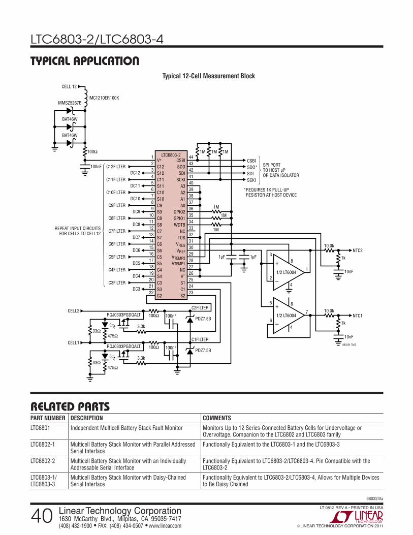
LTC6803-2/LTC6803-4
40680324fa
Linear Technology Corporation1630 McCarthy Blvd., Milpitas, CA 95035-7417 (408) 432-1900 ● FAX: (408) 434-0507 ● www.linear.com LINEAR TECHNOLOGY CORPORATION 2011
LT 0812 REV A • PRINTED IN USA
RELATED PARTS
TYPICAL APPLICATIONTypical 12-Cell Measurement Block
PART NUMBER DESCRIPTION COMMENTS
LTC6801 Independent Multicell Battery Stack Fault Monitor Monitors Up to 12 Series-Connected Battery Cells for Undervoltage or Overvoltage. Companion to the LTC6802 and LTC6803 family
LTC6802-1 Multicell Battery Stack Monitor with Parallel Addressed Serial Interface
Functionally Equivalent to the LTC6803-1 and the LTC6803-3
LTC6802-2 Multicell Battery Stack Monitor with an Individually Addressable Serial Interface
Functionally Equivalent to LTC6803-2/LTC6803-4. Pin Compatible with the LTC6803-2
LTC6803-1/LTC6803-3
Multicell Battery Stack Monitor with Daisy-Chained Serial Interface
Functionality Equivalent to LTC6803-2/LTC6803-4, Allows for Multiple Devices to Be Daisy Chained
V+
C12S12C11S11C10S10C9S9C8S8C7S7C6S6C5S5C4S4C3S3C2
CSBISDOSDI
SCKIA3A2A1A0
GPIO2GPIO1WDTB
NCTOS
VREGVREF
VTEMP2VTEMP1
NCV–
S1C1S2
123456789
10111213141516171819202122
DC12
DC11
DC10
DC9
DC8
DC7
DC6
DC5
DC4
DC3
C12FILTER
C11FILTER
C10FILTER
C9FILTER
C8FILTER
C7FILTER
C6FILTER
C5FILTER
C4FILTER
C3FILTER
44434241403938373635343332313029282726252423
LTC6803-2
REPEAT INPUT CIRCUITSFOR CELL3 TO CELL12
100nF
1µF 1µF
C2FILTER
10nF
NTC2
NTC1
3
1
4
8
2
100Ω 1M 1M 1M
CSBISDO*SDISCKI
BAT46W
BAT46W
MMSZ5267B
CELL 12
IMC1210ER100K
SPI PORTTO HOST µPOR DATA ISOLATOR
*REQUIRES 1K PULL-UP RESISTOR AT HOST DEVICE
1M
10.0k
10.0k
1k
10nF
680324 TA02
1k
1M
1M
100Ω
3.3k
RQJ0303PGDQALT 100nF
100nF
475Ω33Ω
CELL2
CELL1
PDZ7.5B
C1FILTER
100Ω
3.3k
RQJ0303PGDQALT
475Ω33Ω
PDZ7.5B
–
+1/2 LT6004
5
7
4
8
6–
+1/2 LT6004