low-power circuit techniques for battery …jungfrau.usc.edu/pubs/jay-thesis.pdf · iii...
TRANSCRIPT

LOW-POWER CIRCUIT TECHNIQUES FOR BATTERY-POWERED
DSP APPLICATIONS
by
Joong-Seok Moon
______________________________________________________________
A Dissertation Presented to the FACULTY OF THE GRADUATE SCHOOL
UNIVERISITY OF SOUTHERN CALIFORNIA In Partial Fulfillment of the Requirement for the Degree
DOCTOR OF PHILOSOPHY (ELECTRICAL ENGINEERING)
August 2003
Copyright 2003 Joong-Seok Moon

ii
Dedication
This dissertation is dedicated to all of my family members for their love,
encouragement and support.

iii
Acknowledgements
I always wondered when I would write the acknowledgements of the dissertation. It
has been so long since I started my study thus I got lost in despair on many occasions.
So many people helped, encouraged and advised me during this once seemingly
endless battle. Putting my enormous gratitude toward them into words seems to be
the most difficult task, but let me try. First, there is Prof. Peter Beerel. He graciously
accepted me into his group in the middle of my Ph.D. work and continuously
encouraged me to finish my dissertation. His amazing ability to turn things from
messy to crystal clear always makes me wonder. Without his help, most of works if
not all in this dissertation wouldn’t exist. Second, Dr. Jeff Draper deserves my
utmost gratitude for his support, encouragement, generosity and advice. During my
last two years in ISI, I got all the support from him every graduate student would
wish for: great research projects, strong trust and invaluable technical advice. Third,
I would like to appreciate Dr. Pedro Diniz for being a member of my Ph.D.
committee and giving me many precious feedbacks. In addition, I would like to
appreciate Prof. Massoud Pedram and Prof. Sandeep Gupta for their invaluable
feedback during my Ph.D. qualifying exam. Fourth, it is hard to imagine my research
without the guidance from Dr. Bill Athas. Every single circuit presented in this
dissertation originates from discussions with him. I really wished I would spend
more time with him when he left ISI, so I am going to start to work with him again.
It is going to be an enjoyable challenge. Fifth, I would like to thank Prof. Alvin

iv
Despain and Prof. Deog-Kyoon Jeong who introduced the fields of computer
architecture and VLSI to me.
There are many friends at USC with whom I enjoyed a strong friendship. First, there
are three guys I and my family enjoyed spending time together: Sangyun Kim, Ihn
Kim and Kisup Chong. We share grief and delight together all the time. I certainly
hope to continue our friendship in the same way. Second, USC Asynchronous
CAD/VLSI group members have been great to mingle with: Recep Ozdag, Marcos
Ferretti, Sunan Tugsinavisut, Hakan Durmus and Hoshik Kim. We never pronounced
each others last names correctly, but it didn’t bother us at all to enjoy getting
together. Third, I am lucky to have a lot of good friends at ISI. In particular, I would
like to thank Joonseok Park, Taek-Jun Kwon, Chang-Woo Kang and Dongho Kim
for wasting their time to listen to my grumblings. I am going to miss them a lot.
Other friends outside USC need to be mentioned here for their perennial support and
friendship. Especially, Clark Joonseok Kim and Yong-Seok Choi have been my best
friends and will be forever.
Last but not the least, there are my whole family members. Mom, thank you and I
love you. I wish Dad would watch his son to graduate, but I am sure he will be very
proud of us. My parents-in-law, I am so glad to have you. Thank you for all of your
support and encouragement. Sisters, brother, brother-in-law and sister-in-law, thank
you for being with me. My son, Jason, thank you for being in this world. You are the

v
most precious gift I ever got. I promise I will be a good father from now on. Hyun-
Jung, my dear wife, it is not my degree but our degree. I dedicate my post-graduate
life to you as well as this dissertation.

vi
Table of Contents
Dedication ....................................................................................................................ii
Acknowledgements .....................................................................................................iii
Table of Contents ........................................................................................................vi
List of Figures ...........................................................................................................viii
List of Tables..............................................................................................................xii
Abstract .....................................................................................................................xiii
Chapter 1 ......................................................................................................................1
1.1 Background of low-power CMOS digital design.............................................2 1.1.1 Technology...............................................................................................3 1.1.2 Circuit and logic.......................................................................................4 1.1.3 Architecture..............................................................................................6 1.1.4 Algorithm and system ..............................................................................7
1.2 Contributions....................................................................................................7 1.3 Organization.....................................................................................................9
Chapter 2 ....................................................................................................................11
2.1 Motivation......................................................................................................11 2.2 Architecture....................................................................................................12 2.3 Read timing based on the handshaking protocol ...........................................14 2.4 Circuits ...........................................................................................................16
2.4.1 Static memory cell..................................................................................16 2.4.2 Sense amplifier and latch .......................................................................18 2.4.3 Decoder cell ...........................................................................................19 2.4.4 Write driver ............................................................................................19 2.4.5 Flip-flop for address inputs ....................................................................20 2.4.6 Read controller: rdec_en signal generator..............................................22 2.4.7 Read controller: sa_en signal generator .................................................23 2.4.8 Read controller: precharge signal generator ..........................................24 2.4.9 Read timing ............................................................................................25
2.5 Performance and power simulation results ....................................................26 2.6 Implementation: DC-2 32-bit general-purpose microprocessor ....................30
Chapter 3 ....................................................................................................................32
3.1 Motivation......................................................................................................32

vii
3.2 Architecture....................................................................................................34 3.3 Circuits ...........................................................................................................36
3.3.1 Sequencer cell ........................................................................................36 3.3.2 Bank sequencer ......................................................................................38 3.3.3 Sequencer cell ........................................................................................39 3.3.4 Overall read operation summary............................................................42
3.4 Test chip and measurement results ................................................................43 Chapter 4 ....................................................................................................................47
4.1 Motivation......................................................................................................47 4.2 Current-fed voltage pulse-forming network...................................................52 4.3 Theoretical analysis of current-fed voltage pulse-forming network ..............56 4.4 Voltage-pulse driven pulse-forming network ................................................62
4.4.1 Voltage-pulse driven network for DC current source elimination.........63 4.4.2 A tank capacitor for a positive-swing waveform ...................................69
4.5 Measurement ..................................................................................................71 Chapter 5 ....................................................................................................................81
5.1 Motivation......................................................................................................81 5.2 Architecture....................................................................................................85 5.3 Timing and circuits ........................................................................................86
5.3.1 Local clock generation ...........................................................................86 5.3.2 Controller ...............................................................................................87 5.3.3 Read operation .......................................................................................89 5.3.4 Write operation.......................................................................................93 5.3.5 Overall timing for FIR filtering..............................................................94
5.4 Issues with the clock distribution network.....................................................96 5.4.1 Global and hierarchical clock trees ........................................................96 5.4.2 Resonant and conventional clock drivers...............................................98
5.5 Implementation ............................................................................................102 5.6 Kaiser-window low-pass FIR filter..............................................................105 5.7 Simulation results.........................................................................................106
Chapter 6 ..................................................................................................................112
References ................................................................................................................115
Appendix ..................................................................................................................122

viii
List of Figures
Figure 1: A block diagram of an N x M Register File ...............................................13
Figure 2: Micro-operation dependency flowchart......................................................14
Figure 3: A Timing diagram of the register file read operation.................................15
Figure 4: A block diagram of the read controller.......................................................16
Figure 5: A schematic of a three-port SRAM cell .....................................................17
Figure 6: Write operations for two different values on the SRAM cell.....................17
Figure 7: A schematic of a sense amplifier and a latch..............................................18
Figure 8: A timing diagram of the sense amplifier and latch.....................................18
Figure 9: A schematic of a 4-to-16 address decoder cell ...........................................20
Figure 10: A schematic of a write driver ...................................................................20
Figure 11: An original sense-amplifier based flip-flop..............................................21
Figure 12: A modified flip-flop that resets outputs to zero at the negative edge of a clock signal..........................................................................................................21
Figure 13: A schematic of the read controller: a rdec_en signal generator ...............23
Figure 14: A schematic of the read controller: a sa_en signal generator...................23
Figure 15: A schematic of the read controller: a precharge signal generator............24
Figure 16: Signal transitions of a read operation .......................................................25
Figure 17: Worst-case delay of the register files .......................................................26
Figure 18: Relative power dissipation of the read operation .....................................29
Figure 19: A microphotograph of the DC-2 microprocessor .....................................31
Figure 20: A block diagram of an N x M SAM .........................................................34
Figure 21: A block diagram of a 64x16-b SAM composed of four 16x16-b SAM banks....................................................................................................................35

ix
Figure 22: A schematic of the sequencer cell ............................................................37
Figure 23: A timing diagram of the sequencer cell....................................................37
Figure 24: A schematic of the bank sequencer ..........................................................38
Figure 25: A timing diagram of the bank sequencer..................................................39
Figure 26: A schematic of the read controller............................................................40
Figure 27: A timing diagram of read controller .........................................................41
Figure 28: Signal transitions of the read operation ....................................................42
Figure 29: A microphotograph of the test chip ..........................................................43
Figure 30: Measured power dissipation of the worst-case read operations ...............45
Figure 31: Measured power dissipation of the worst-case write operations..............45
Figure 32: A single-rail resonant clock driver (Flyback circuit) ...............................48
Figure 33: All-resonant blip driver ............................................................................48
Figure 34: A harmonic resonant rail driver containing three harmonic terms...........49
Figure 35: A trapezoidal-wave voltage signal with slope VO/(2*T).........................52
Figure 36: Current-fed voltage pulse-forming network (CFVPN). ...........................53
Figure 37: An equivalent network of Figure 36 containing a capacitance CL that can represent an on-chip clock load...........................................................................55
Figure 38: An Equivalent network of Figure 37 driven by a voltage pulse. ..............63
Figure 39: Practical approximation of the network shown in Figure 38....................63
Figure 40: Frequency response of the network shown in Figure 39 (Vo(s)/Vi(s)).....66
Figure 41: The proposed network with the parasitic resistance of inductors.............66
Figure 42: Frequency response of the network shown in Figure 41 for the first two harmonic frequencies (a) magnitude (b) phase. ..................................................68
Figure 43: DC steady-state for the network (a) without CT (b) with CT. ...................69
Figure 44: A voltage-pulse driven harmonic resonant rail driver. .............................71

x
Figure 45: Normalized power dissipation (P/fCLV2) and transition time versus resistance R. fCLV2 is the theoretical conventional power dissipation to drive load capacitance CL. ............................................................................................73
Figure 46: A scope trace of output waveform for the 2nd-order driver at 1MHz. ......75
Figure 47: A scope trace of output waveform for the 3rd-order driver at 1MHz. ......75
Figure 48: A FFT-enabled scope trace of waveform for the 4th-order driver at 1MHz..............................................................................................................................76
Figure 49: A scope trace of output waveform for the 2nd-order driver at 10MHz. ....76
Figure 50: Normalized power dissipation versus load capacitance (CL). All components except CL are kept same as designed for 100pF CL.........................77
Figure 51: Clock jitter versus load capacitance (CL). ................................................78
Figure 52: Normalized power dissipation versus clock cycle variation. ...................79
Figure 53: A tapped delay line implementation of N-tap FIR filter. .........................82
Figure 54: A generic DSP architecture for FIR filter.................................................82
Figure 55: A block diagram of a N-tap FIR filter ......................................................85
Figure 56: A timing diagram of the read operation of SAM with a newly added complete signal....................................................................................................87
Figure 57: A block diagram of the 64-tap FIR filter controller. ................................88
Figure 58: A timing diagram of the 64-tap FIR filter controller................................88
Figure 59: A starting location of the data memory for each sample. .........................89
Figure 60: A timing diagram of read accesses for the 64-tap FIR filter. ...................90
Figure 61: A modified read controller of the SAM to enable an initial read access by pphi ......................................................................................................................90
Figure 62: A block diagram of the data memory to generate the local clock signal lphi.......................................................................................................................91
Figure 63: A timing diagram of Figure 62. Each bank is assumed to have only two rows to simplify the diagram...............................................................................92

xi
Figure 64: A modified read controller of the multi-bank SAM to enable an initial read access by pphi. .............................................................................................93
Figure 65: A timing diagram of write operations.......................................................94
Figure 66: An overall timing diagram of FIR filtering ..............................................95
Figure 67: Hierarchical clock tree generation for FIR filter banks. ...........................97
Figure 68: Conventional clock tree generation with global clock distribution..........98
Figure 69: Two clock tree driving scheme: (a) Single driver scheme (b) distributed buffer scheme ......................................................................................................99
Figure 70: Serpentine clock distribution network....................................................100
Figure 71: Balanced H-tree clock distribution network...........................................100
Figure 72: A layout plot of the 16-tap FIR filter......................................................103
Figure 73: A layout plot of the 64-tap FIR filter......................................................104
Figure 74: Frequency response of two low-pass FIR filters. ...................................105
Figure 75: FFT plot of the speech sampled at 16KHz .............................................106
Figure 76: Average cycle time of two FIR filters. ...................................................107
Figure 77: Energy/sample plot for two FIR filters...................................................108
Figure 78: Power breakdown of two FIR filters. .....................................................109
Figure 79: Waveform plot for vx(t) in Eq. 49. ..........................................................125

xii
List of Tables
Table 1: Worst-case power dissipation of the register files at the maximum clock frequencies for a give supply voltage..................................................................28
Table 2: Summary of the process technology and the test chip.................................44
Table 3: Component Values for Network of Figure 36 .............................................54
Table 4: Measured data of second, third, and fourth square-wave harmonic resonant rail driver for various clock frequencies and load capacitances. The first three rows are data for driving 97.8pF load capacitance at different clock frequencies and the last row shows data for different load capacitances at 1MHz. Theoretical and measured values of each component are also shown for comparison. .........72
Table 5: Summary of the process technology and the test chip...............................102
Table 6: Clock cycle time variation = (Tmax/min – Tavg) / Tavg...................................108
Table 7: Effective clock capacitance of the conventional clock tree for filter banks...........................................................................................................................110
Table 8: Effective clock capacitance of the balanced H-tree...................................110

xiii
Abstract
One of the most crucial factors that fuel the needs for low-power VLSI chips is the
increased market demand for portable consumer electronics powered by batteries.
The craving for smaller, lighter and more durable electronic products indirectly
translates to low-power requirements.
This dissertation proposes various circuit techniques for the memory and the clock
network, which are among the major power consuming components in many
portable DSP applications. First, a general-purpose high-performance low-power
register file design is presented. Based on self-resetting postcharge logic, the design
provides wide voltage scalability and avoids short-circuit current. Second, we
present a sequential access memory design to further optimize power dissipation and
performance by replacing decoders with novel sequencers. The sequential access
pattern for memory is ubiquitous in many DSP applications such as FIR filtering and
FIFOs. Power dissipation required for address sequencing logic, decoders and
drivers for address lines are eliminated by exploiting this characteristic. Third, we
present an energy-efficient clock generator based on the harmonic resonant circuit
technique. Significant power dissipation for a clock network is reduced because most
of the charge is recovered by driving the network resonantly. Experimental results
are presented for a comparison with conventional clock drivers and various
characteristics of the proposed circuit are quantified. Finally, a novel FIR filter
design is presented as a case study to show the feasibility of the proposed circuit

xiv
techniques for a real DSP application. The high-frequency clock signal needed for
FIR filter operations is locally generated from a self-resetting memory control signal.
In this way, the system clock frequency is reduced to the sample rate. The datapath is
designed in the standard ASIC design methodology without any special interfacing
logic.

1
Chapter 1
INTRODUCTION
The increasing demand for low power dissipation has been driven by a growing class
of portable, battery-powered applications that demand ever-increasing functionality
and battery life. Power dissipation plays the most important role in the design and
implementation of many, if not all, of these applications due to the contingent
requirements on battery dimension and weight. Traditionally, Nickel-Cadmium
batteries had been used in most applications that require rechargeable batteries.
Nickel-Metal Hybrid (Ni-MH) and Lithium-Ion batteries recently became more
popular batteries for portable applications for their improved energy density and
reduced toxic heavy metals [52]. The energy capacity of batteries has been
improving over the last two decades, but at a very slow pace [22]. Moreover, the
energy stored in a battery cannot be extracted to the full extent due to the strong
dependence of the energy capacity on the mean value of the discharge current as well
as the portion of energy that is wasted by the DC/DC converter [52]. With a
projection of this slow pace and limitation of battery technology, unless low-power
approaches are adopted in various aspects of systems, current and future portable
devices will suffer significantly from either very short battery life or unreasonably
heavy battery packs.

2
Many of these battery-powered devices perform digital signal processing (DSP)
functions [50], including FIR/IIR (finite/infinite impulse response) filtering
[41][44][45], CODEC (coding and decoding) [58][1], DCT/IDCT (discrete cosine
transform) [11][71], and FFT (fast Fourier transform) [12][31]. In these devices,
maintaining a given level of computation or throughput is a common concept, in
which there is no advantage in performing the computation faster than a given rate
since the hardware will simply have to wait until further computation is required.
This is in sharp contrast to general-purpose processing, where the goal is often to
provide the fastest possible computation without bound [18]. This enables a variety
of techniques that lower power dissipation while maintaining a constant throughput.
Based on these constraints, the motivation for this research is to investigate practical
low-power circuit solutions for battery-powered DSP devices to increase the battery
life at a given throughput.
1.1 Background of low-power CMOS digital design
The sources of power dissipation in CMOS circuits can be classified as dynamic,
short circuit and leakage power [17][57]. For most CMOS designs, the dynamic
power dissipation is the main source of power dissipation and is given by
210 DDL VCfP ⋅⋅⋅= →α Eq. 1
where 01 is the switching activity of the signals involved, CL is the load
capacitance, VDD is the supply voltage level of the system and f is the average data

3
rate, which is usually the clock frequency in a synchronous system [17]. This
equation suggests that there are three degrees of freedom in the low-power design
space: voltage, physical capacitance, and switching activity [51]. To reduce these
fundamental elements of power dissipation, all levels of the design hierarchy can be
approached. The following sections briefly summarize the power dissipation
optimization at each level of the design hierarchy.
1.1.1 Technology
As shown in Eq. 1, dynamic power dissipation is quadratically proportional to the
supply voltage. Therefore, reducing the supply voltage is the most effective means of
minimizing the power dissipation. However, lowering VDD for a given technology
leads to lower performance. In particular, as VDD approaches the transistor threshold
voltage, the performance of the system decreases exponentially. The most popular
technology optimization for low power dissipation is to reduce the threshold voltage
of the device [64]. Reducing the threshold voltage allows the supply voltage to be
scaled down without loss of performance. There is a limit for the threshold voltage
scaling due to the increase in the subthreshold currents as the threshold voltage
scales down. Moreover, the reduced noise margin may adversely affect the system
stability. Therefore, the optimal threshold voltage must compromise between
improvement of current drive at low supply voltage operation and control of the
subthreshold currents and noise margin.

4
1.1.2 Circuit and logic
Contrary to the technology optimization where reducing the supply voltage level is a
major goal, at the circuit and logic levels, all three elements (voltage, physical
capacitance and switching activity) are considered to reduce power dissipation. A
myriad of low-power approaches has been proposed at this level and some
representative works are summarized as follows.
A. Low voltage swing circuit design
At a given supply voltage, the outputs of full-swing CMOS gates make rail-to-rail
transitions. In low voltage swing circuit design, power dissipation is reduced by
limiting the voltage swing on the output node [74][23]. However, care must be taken
to ensure reduced swing nodes do not lead to increased static power dissipation. In
particular, interfaces with conventional gates require special receivers to convert low
swing input to full swing output, which may incur large circuit overheads. To limit
this overhead, low voltage swing techniques target only high-capacitance nodes such
as data buses.
B. Gated clocking for logic level power-down
In synchronous designs, the logic between registers is continuously computing every
clock cycle based on its new inputs. To reduce the power in synchronous designs, it
is very effective to minimize switching activity by powering down logic blocks when

5
they are not performing useful operations. Self-timed or asynchronous circuits have
an inherent power-down feature for unused blocks, since transitions occur only when
requested [40]. However, generation of completion signals indicating the outputs of
the logic block are valid generally requires additional circuit overhead. In
synchronous designs, this can be done using gated clocking techniques that enable
registers only when necessary [48][14][70].
C. Energy-recovery and adiabatic circuit design
In energy-recovery circuit design [57][10], circuit energy that would otherwise be
dissipated as heat is instead conserved for later reuse. This is a completely different
approach from other conventional techniques where the goal is to minimize the
energy delivery that will be completely dissipated as heat. The DC power supply is
replaced with an AC power source to enable bidirectional energy delivery. Clock
signals generated by resonant circuits have been widely adopted as the cheapest
source of AC power for these applications [7].
In adiabatic circuit design [17][6], on the other hand, slowing down the charge
transfer between nodes reduces the power dissipation due to the resistance of the
switches usually implemented as transistors. These two techniques are commonly
combined to maximize energy efficiency [9][8].

6
D. Other methods
Other circuit and logic minimization techniques include
• High-efficiency DC/DC conversion circuit design [5][62]
• Logic minimization and technology mapping [33][65][72]
• Transistor sizing and logic manipulation [18][17]
1.1.3 Architecture
As we scale down the supply voltage for low power dissipation, the performance of a
device decreases due to the reduced conduction current of transistors. One way to
maintain throughput while reducing the supply voltage is to utilize a parallel
architecture, either using hardware duplication or pipelining [18][17]. The amount of
parallelism needed to achieve a given throughput depends on the level of the reduced
supply voltage. However, as the supply voltage approaches the threshold voltage, the
degradation in performance increases dramatically and the overhead associated with
parallel architectures increases overall power. The optimum voltage can be found
where further reduction in the supply voltage makes the power dissipation increase.
The area overhead of pipelining can be much smaller than the hardware duplication
approach, since only stage registers have to be added instead of complete hardware
duplication. However, partitioning into several pipeline stages for some hardware
requires more pipeline registers to accommodate the intermediate signals. Clearly

7
these two approaches can be used simultaneously. Other architecture driven low-
power techniques are
• Choice of number representation to minimize switching activity [63]
• Reordering input signals [18][17]
• Logic depth balancing to reduce glitching activity [2][2]
1.1.4 Algorithm and system
The choice of algorithm can make a huge impact on the total power dissipation of the
system, such as reduction of arithmetic operations and memory accesses by
transforming a given algorithm [49]. Other examples at this level include operator
reduction [29] and constant propagation [54] [54]. In system-level power
optimization, battery design, intelligent power management and OS support for sleep
levels are found in many design examples.
1.2 Contributions
As pointed out in the previous section, the algorithm and system levels have the most
significant effect on the total power dissipation of the system. However, for a given
algorithm and system specification, we must approach other levels of the design
hierarchy for further reduction of the power dissipation. In particular, circuit
techniques for low power dissipation can have a major impact because some circuits
are repeated thousands of times on a chip and many high-capacitance nodes are

8
switching regularly. This dissertation proposes various circuit techniques for
memory blocks and a clock network, which are among the major power consuming
components in many portable DSP applications. It then presents a case study to show
the feasibility of the proposed circuit techniques in a real DSP application and
quantifies the improvements compared to traditional designs. The following
paragraphs summarize the contributions of this dissertation.
A. Register file design
First, we present a high-speed and low-power register file design. A novel read
controller using self-resetting postcharge logic is presented to minimize static power
dissipation and to increase voltage scalability for read operations. This circuit
technique can be extended to a large SRAM design with a small modification. In
addition, the proposed register file design can be easily converted for a self-timed
computation environment.
B. Sequential access memory design
Second, we present a sequential access memory design to further optimize power
dissipation and performance by replacing decoders with novel sequencers. The
sequential access pattern for memory is ubiquitous in many DSP functions like FIR
filters and FIFOs. The power dissipation required for address sequencing logic,
decoders and drivers for address lines are eliminated by exploiting this characteristic.

9
C. Harmonic resonant clock generator design
Third, we present an energy efficient clock generator based on the harmonic resonant
circuit technique. Significant power dissipation for a clock network can be saved
because most of the charges can be recovered by driving the network resonantly.
Experimental results are presented to compare with a conventional clock driver, and
various characteristics of the proposed circuit are quantified. The circuit performs
well in the low to mid clock frequency range with a significant saving in power
dissipation.
D. FIR filter implementation
Fourth, a novel FIR filter design is presented as a case study to show the feasibility
of the proposed circuit techniques in a real DSP application. A self-resetting data
memory is configured such that it generates a stoppable clock that is synchronously
started and asynchronously stopped. In this way, the system clock frequency is
reduced to the sample rate. The circuit overhead is minimal by utilizing most of
existing signals. The datapath is designed in the standard ASIC design methodology
without any special interfacing logic.
1.3 Organization
The remainder of this dissertation is organized as follows. Chapter 2 presents the
register file design which is the foundation of our memory design techniques

10
throughout this dissertation. Our sequential access memory design is presented in
Chapter 3. Chapter 4 then describes the harmonic resonant clock generator design.
The memory-triggered self-timed FIR filter is presented in Chapter 5 as a case study
utilizing our proposed circuit techniques in a real DSP application. Chapter 6
presents conclusions and some issues for future research.

11
Chapter 2
LOW-POWER REGISTER-FILE DESIGN
2.1 Motivation
Register files used in the design of microprocessors or digital signal processors are
often implemented as multi-port on-chip SRAMs. For microprocessors, a low-power
high-speed register file is important because almost every instruction in all
instruction sets requires read and/or write accesses to the register file. In digital
signal processors, most of the applications require streaming data operations, which
require accesses to a small window of a data stream repeatedly. Therefore, the
pursuit of low-power high-speed register file design has lead to numerous design
techniques and implementations [36][3][37][46][24]. One prosperous avenue for
register file design is to use self-resetting postcharge logic [32][30][4][47]. Self-
resetting postcharge logic exploits asynchronous and self-timed circuit concepts
without incurring the typical circuitry overhead of asynchronous circuitry. In
particular, this technique is highly effective for memory design because dummy
memory cells [47][4] and reset inverter chains [32][4] that effectively simulate the
actual timing can simplify the completion detection signal generation with a small
overhead. However, ensuring design robustness is relatively difficult for this
technique because unexpected timing margin errors from process variations can
cause failures in functionality, which cannot be overcome by changing the clock

12
frequency or the supply voltage. As a result, an increased susceptibility to process
variations requires significant design effort and sophisticated CAD tools.
We present a novel register file design using self-resetting postcharge logic. Reset
inverter chains are replaced with the read controller that implements a hand-shaking
protocol. Several benefits arise from using a hand-shaking protocol rather than reset
inverter-chains. First, susceptibility to process variations is minimized, and thus
design effort can be significantly reduced. Second, static power dissipation is
minimized by defining a sequence of control signals such that static currents that
typically arise due to overlap between bitline precharging and wordline driving are
mostly eliminated. In addition, dynamic power dissipation incurred by the reset
inverter chains can be removed. The proposed read controller is triggered by a single
clock edge so that it can generate control signals for a register file that uses single-
phase or multi-phase clocks. The proposed register file was implemented in 0.5m
CMOS technology for a general-purpose microprocessor [43][9] [61].
2.2 Architecture
Figure 1 shows a block diagram of our proposed three-port N x M-bit register file
allowing two read and one write accesses simultaneously. A register array, three
decoders (two for read and one for write), write drivers, two sense amplifier arrays
with latches, flip-flops for address inputs, precharge logic and read/write controllers
are shown.

13
Figure 1: A block diagram of an N x M Register File
To enable a read operation, the read enable signal (RdEn) must be asserted. Then,
upon the rising edge of the clock signal, the read decoder enable signal (rdec_en) is
raised to enable the decoders to assert the wordline signal (rwl[k]) corresponding to
the current input read addresses (raddrA[log2N-1:0], raddrB[log2N-1:0]). This
activates the associated memory cells and dummy cell, driving the read bitlines
(rbitA[M-1:0],rbitB[M-1:0]) and the dummy bitline (dumbit), respectively. The
write operation is similar except the write bitlines (wbit[M-1:0]) are not precharged.
The proposed handshaking protocol, which will be explained in the next section, is
integrated in the read controller.

14
2.3 Read timing based on the handshaking protocol
The read controller of the register file has seven micro-operations that constitute a
read access of the register file. These are: 1. Wait for detect read request, 2. Enable
address decode and disable bitline precharge, 3. Enable wordline, 4. Start memory
read and enable sense amplifiers, 5. Detect completion of memory read, 6. Disable
wordline and sense amplifier then latch read output, 7. Enable bitline precharge. The
flowchart of Figure 2 shows the dependencies between these micro-operations.
Figure 2: Micro-operation dependency flowchart
Maintaining these dependencies ensures the functionality and minimizes static power
dissipation mainly caused by the overlap between bitline precharge and memory
access. A dummy bitline and dummy memory cells are used to track the latency of

15
reading bitlines and detect the completion of a memory access. The register file is
triggered by the rising edge of the clock. However, it can be easily adapted to be
triggered by a falling edge of the clock. A timing diagram of the register file is
presented in Figure 3 with annotations to specify the corresponding micro-operations
in Figure 2.
Figure 3: A Timing diagram of the register file read operation
All signal interactions of read operations are directed by three control signals –
rdec_en, sa_en, precharge – with dumbit signal and clock. Figure 4 shows the block
diagram of the read controller, which is composed of three blocks: decoder enable
signal, sense amplifier enable signal, and precharge signal generators. By following
the sequence shown in Figure 2, interconnections between these blocks can be easily
understood. The rdec_en signal is triggered by the clock signal, while the dumbit
signal triggers the sa_en signal. The rdec_en signal triggers the precharge signal.
Notice that the precharge signal and the rwln[N-1:0] signals are completely non-
overlapping, suggesting that the static currents between memory cells and precharge

16
transistors can be eliminated. A detailed circuit implementation will be described in
the next section.
Figure 4: A block diagram of the read controller
2.4 Circuits
2.4.1 Static memory cell
Figure 5 shows the three-port SRAM circuit schematic. A single-ended scheme is
used both for write and read operation to reduce power dissipation. Write operations
for two different values are depicted in Figure 6. A differential mode is used for
writing high values on node q while a single-ended mode is used for writing low
values. Therefore, the latency for write operations is dependent upon the write data
value. However, this latency variation does not constrain the performance because
write operations are inherently much faster than read operations in the SRAM design.

17
Figure 5: A schematic of a three-port SRAM cell
Figure 6: Write operations for two different values on the SRAM cell
18
2.4.2 Sense amplifier and latch
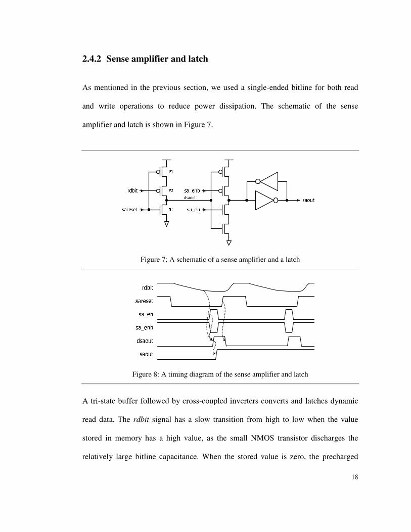
As mentioned in the previous section, we used a single-ended bitline for both read
and write operations to reduce power dissipation. The schematic of the sense
amplifier and latch is shown in Figure 7.
Figure 7: A schematic of a sense amplifier and a latch
Figure 8: A timing diagram of the sense amplifier and latch
A tri-state buffer followed by cross-coupled inverters converts and latches dynamic
read data. The rdbit signal has a slow transition from high to low when the value
stored in memory has a high value, as the small NMOS transistor discharges the
relatively large bitline capacitance. When the stored value is zero, the precharged

19
high value on the rdbit node is retained. Therefore, instead of connecting this slow
signal to the conventional buffer/inverter to convert into the fast full-swing signal,
only a PMOS transistor (P2) is connected to the rdbit signal. As rdbit has only
negative going transition, the proposed circuit can eliminate static currents from the
slow input slew rate. The NMOS transistor (N1) connected to the sareset signal is
turned off during read operations. When a read operation is completed, this signal
resets the internal node (drdout) to zero. The sareset signal is generated simply as the
inverted form of the precharge signal. A timing diagram of the sense amplifier and
latch is presented in Figure 8.
2.4.3 Decoder cell
Since the number of address inputs is modest (3-6) in the register file design, a pure
single-level dynamic NAND gate is used for decoder cells of the register file. Figure
9 shows a schematic of a four input address decoder cell. To prevent the charge
sharing problem resulting from a long NMOS chain, two weak PMOS (P1, P2)
transistors are added.
2.4.4 Write driver
A simple tri-state buffer is used for the single-ended write driver circuit as shown in
Figure 10.

20
Figure 9: A schematic of a 4-to-16 address decoder cell
Figure 10: A schematic of a write driver
2.4.5 Flip-flop for address inputs
A normal flip-flop output cannot be used for the dynamic gates since a negative
transition of the output during the evaluation phase of the dynamic gate can
accidentally discharge the precharged value. A latch works well with the dynamic
gate, but more than one clock phase is required. To avoid a multi-phase clocking

21
design and to combine dynamic logic with an edge-triggered input, the flip-flop is
designed such that the output of the flip-flop always has a positive-going signal. This
can be done by resetting the output of the flip-flop to low at the negative edge of the
clock signal.
Figure 11: An original sense-amplifier based flip-flop
Figure 12: A modified flip-flop that resets outputs to zero at the negative edge of a clock signal

22
Figure 11 shows the original flip-flop design based on the sense-amplifier structure
used in StrongARM microprocessors [42]. Cross-coupled NAND gates at the output
stage hold the latched values during the low phase of the clock signal. By replacing
these NAND gates with the cross-coupled NOR gates, we can easily convert this
flip-flop to reset the output at the negative edge of the clock signal. The modified
flip-flop circuit is presented in Figure 12.
2.4.6 Read controller: rdec_en signal generator
Read operations are initiated by enabling the read decoders. The rdec_en signal
generated by the circuit shown in Figure 13 starts the evaluation of address decoding.
During the low phase of the clock signal, node A is precharged. At the rising edge of
the clock, node B is pulled down and the rdec_en signal is asserted to high. After the
read operation is completed, the sa_en signal is asserted by the sense amplifier
enable signal generator. At the rising edge of the sa_en signal, the rdec_en signal
resets to low value. The sa_en signal can arrive either during high phase or low
phase of the clock signal depending on the supply voltage and operating frequency.
The proposed circuit is designed such that branch A is turned on only for the positive
transition of the rdec_en signal and branch B for the negative transition regardless of
the clock phase.

23
2.4.7 Read controller: sa_en signal generator
The sa_en signal generator uses the same topology as the sense amplifier circuit
shown in Figure 7 except the tri-state buffer in the sense amplifier is replaced by an
n-latch circuit as shown in Figure 14. The dumbit signal is used to simulate and
detect the actual memory access latency. When the sa_en signal is asserted by the
dumbit signal, it is assumed that all other memory accesses are completed.
Figure 13: A schematic of the read controller: a rdec_en signal generator
Figure 14: A schematic of the read controller: a sa_en signal generator

24
2.4.8 Read controller: precharge signal generator
Figure 15 shows the schematic of the precharge signal generator. To eliminate static
power dissipation, we must disable the bitline precharging before the read operation
and enable again right after the read operation is completed. The rdec_en signal is
used to disable the bitline precharging since the rising edge of this signal is the first
transaction of the read operation. As suggested in Figure 3, the completion of the
read operation can be defined by the falling edge of the sa_en signal. Therefore, the
sa_en signal is connected to one of the PMOS transistors to restart the bitline
precharging.
Figure 15: A schematic of the read controller: a precharge signal generator

25
2.4.9 Read timing
Figure 16 summarizes the signal transitions for a read operation. Each transition is
identified and numbered in the increasing order of operation sequence. Transitions
with the same number are concurrent.
Figure 16: Signal transitions of a read operation

26
2.5 Performance and power simulation results
The proposed register file was designed and implemented in a 0.5-µm technology for
a general-purpose microprocessor and a hearing-aid feedback cancellation processor.
Extensive PowerMill and HSPICE simulations were performed to measure the
worst-case power dissipation and access time of the register file. Three different
configurations - 8 x 32b, 16 x 32b, 32 x 32b - were designed. Figure 17 shows the
worst-case delay of three register files at various supply voltages.
1 1.5 2 2.5 3 3.50
10
20
30
40
50
60
Vdd
Tclk
(ns)
8 x 3216 x 3232 x 32
Figure 17: Worst-case delay of the register files
As shown in Figure 17, the worst-case delay of the 8 x 32b register file has the
smallest delay for all supply voltages. The difference of the worst-case delay
increases as the supply voltage decreases. The simulated maximum frequency for the

27
three register file configurations was measured as 30MHz (8 x 32b), 24MHz (16 x
32b) and 19MHz (32 x 32b) at 1.2V supply voltage respectively. At 3.3V supply
voltage, the maximum frequency was measured as 300MHz, 250MHz and 222MHz,
respectively. Contrary to a conventional register file design where bitline
precharging is controlled by the clock such that half of the clock cycle is wasted for
the precharging operation, HSPICE simulation shows that only 10-15% of the clock
cycle is consumed for bitline precharging in the presented register file design. This in
turn gives better voltage scalability for high-performance applications.
We measured the worst-case power dissipation at each supply voltage and maximum
frequency by using the following input patterns.
• Read Addresses: 00…0 11…1
• Write Addresses: 00…0 11…1
• Write data: 00…00 11…11
• Read data: 00…00 11…11
Power dissipation for the worst-case pattern was measured from PowerMill
simulation. Table 1 summarizes the power dissipation results at the maximum
frequency.

28
Tab
le 1
: Wor
st-c
ase
pow
er d
issi
patio
n of
the
regi
ster
file
s at
the
max
imum
clo
ck fr
eque
ncie
s fo
r a g
ive
supp
ly v
olta
ge

29
The effective capacitance in the table is calculated by the following equation.
)/( 2
2
DDCLKeff
DDeffCLKDD
VfPC
VCfVIP
⋅=
⋅⋅=⋅= Eq. 2
Simulation results show that this value is relatively independent of the clock
frequency and the supply voltage, suggesting that the static power dissipation is
virtually eliminated. A small increase in the effective capacitance was observed as
the supply voltage increases due to the increased voltage region where both PMOS
and NMOS transistors are turned on simultaneously. Another HSPICE simulation
result shows that the standby current was less than 0.1uA for all operating
conditions. Figure 18 shows the relative read power dissipation for each functional
block of three register file configurations.
14.75% 17.92%22.80%
36.62%
47.94%
51.34%
28.94%
19.00%
16.80%13.74%
11.36%4.93%
5.95% 3.79% 4.12%
0%
10%
20%
30%
40%
50%
60%
70%
80%
90%
100%
8 x 32 16 x 32 32 x 32
Register file size
Rel
ativ
e re
ad p
ow
er d
issi
pat
ion
Read Decoder
Sense Amplifier
Read Controller
Precharging
Read Address Driver
Figure 18: Relative power dissipation of the read operation

30
One thing to notice in the above graph is that the relative power dissipations for
precharging bitlines and driving address lines increase as the size of the register file
increases. The relative power dissipation for the controller decreases because most of
the control signals drive the same bit width. In the next chapter, we will explore a
sequential access memory design where the power dissipation for driving the address
lines can be eliminated.
2.6 Implementation: DC-2 32-bit general-purpose microprocessor
The proposed 32 x 32-b register file was integrated in the DC-2 32-bit general-
purpose microprocessor and fabricated in 0.5-m CMOS technology. Due to the
contingent pin requirement, separate power and speed measurements of the register
file were not performed. Lab measurements show the chip is functional across a
voltage range between 1.2V and 3.6V. The chip microphotograph is presented in
Figure 19.

31
Figure 19: A microphotograph of the DC-2 microprocessor

32
Chapter 3
LOW-POWER SEQUENTIAL ACCESS MEMORY DESIGN
3.1 Motivation
In many DSP applications a large fraction of the power is consumed in memory
accesses [59]. Numerous general-purpose low power and high performance SRAMs
have been proposed, mostly for high-speed designs [37][32]. Self-resetting circuits
triggered with matched delay lines implemented with dummy memory cells
[30][4][47] often yield relatively low-power and high-speed by limiting the power
dissipation in the bitlines and reducing precharge time as shown in the previous
chapter. A few designs have been proposed for low-power memories with special
emphasis on reduction of leakage current for low-threshold voltage devices [35][41].
In many DSP applications SRAM designs do not require random access and often
have strictly sequential read and/or write access patterns. In particular,
programmable FIR filters read/write coefficients and data in a first-in first-out
pattern [41]. The naïve implementation of such structures involves the movement of
data samples each clock cycle using shift registers. However, for low-power
implementations, the memory can be configured as a circular buffer (with a
sequential access pattern) in which pointers rather than data are moved [68]. In
addition, for many digital communication channel decoders, interleavers that are
used to store and re-organize large blocks of data samples can be designed with

33
memories that support random write and sequential reads (or vice versa). Moreover,
sequential access of intermediate data within many channel decoders, including Fano
decoders [60] and turbo decoders [39], is also typical. In all these cases, the naïve
implementation involves using SRAMs despite the fact that the architecture often
accesses data sequentially. This motivates the design of sequential access memories
to eliminate the power dissipation for address decoding.
This chapter presents a novel sequential access memory (SAM) design where
address sequencing logic and decoders are replaced with row sequencers to achieve
high speed and low power. Most of the control signals are generated using efficient
sequencer cells that communicate primarily with neighboring rows only, minimizing
the power dissipation of wordline selection. When combined with typical bank
structures that limit the amount of switched bit-line capacitance of large memories
and efficient self-resetting postcharge logic, power dissipation is largely independent
of memory size. This is in sharp contrast to conventional SRAM designs.
A test chip was fabricated in 0.25-m CMOS technology to evaluate this design. The
chip contains two different dual-port (one read port and one write port) SAM
configurations: one 16x16-b and one 64x16-b, consisting of four 16x16-b banks. The
chip has been tested and is fully functional at operating voltages of 0.67V to 2.5V.
The power dissipation of both SAMs was measured at different voltages and
operating frequencies and found to be within 5% of each other, demonstrating that
power dissipation is largely independent of memory size. With a clock frequency of

34
40MHz at 1.2V, the measured worst-case read power dissipation for the 16x16-b
SAM is 344W and for the 64x16-b SAM is 358W.
3.2 Architecture
Figure 20 shows a block diagram of our proposed dual-port NxM-bit SAM allowing
simultaneous read and write accesses. Two sequencers, one for read accesses and
one for write accesses, are shown as well as controllers and I/O circuitry. Two reset
sequencer signals (RdRst, WrRst) are asserted to independently initialize the read and
write sequencers to point to the first row.
Figure 20: A block diagram of an N x M SAM

35
To enable the read operation, the read enable signal (RdEn) must be asserted. Then,
upon the rising edge of the clock signal, the read sequencer enable signal (rseq_en) is
raised which triggers the sequencer cell associated with the current pointer location
to assert its associated wordline signal (rwl[k]). This activates the associated
memory cells and dummy cell, driving the read bitlines (rbit[M-1:0]) and the
dummy bitline (dumbit), respectively. The sequencer cell also asserts a trigger signal
(rtrig[k+1]) which is combined with the rseq_en signal to activate the next
sequencer, moving the current pointer location to the next row. The reset of the
current sequencer is triggered by the assertion of the next wordline. The write
operation is similar except the write bitlines (wbit[M-1:0]) are not precharged.
Figure 21: A block diagram of a 64x16-b SAM composed of four 16x16-b SAM banks

36
For large N, driving long bitlines leads to increased power dissipation and latency. A
memory bank structure can be easily applied to this SAM structure because most of
the control signals are locally generated. Figure 21 shows a block diagram of a
64x16-b SAM composed of four 16x16-b SAM banks. The banks are daisy-chained
so that the current bank generates a trigger signal to enable the next bank when a
sequencer pointer has reached the last row in the current bank. In the subsequent
cycle, the first wordline of the next bank is fed back to reset the trigger signal
asserted in the previous cycle. Tri-state buffers are used for I/O circuitry of each
bank so that only one of the banks is connected to the common input/output buses.
3.3 Circuits
3.3.1 Sequencer cell
Figure 22 and Figure 23 show a schematic of the sequencer cell and its timing
diagram. Initially, for the current sequencer cell trig[k] is high while all other trigger
signals are low. In addition, both triggen and wl[k] are low. Upon the assertion of the
sequencer enable (seq_en), the wordline signal (wl[k]) is asserted via a dynamic
AND gate. When seq_en is de-asserted, wl[k] is de-asserted and a short pulse
(triggen) is generated by a NOR gate to assert the subsequent trigger signal
(trig[k+1]), using a jam-latch (pulse-to-level converter). Notice that trig[k+1] is
asserted approximately three gate delays after seq_en goes low to avoid two
wordline signals being activated simultaneously. The trig[k+1] signal is reset by the
assertion of the wordline signal wl[k+1] at the next read cycle.

37
Figure 22: A schematic of the sequencer cell
Figure 23: A timing diagram of the sequencer cell
To reset the SAM, the trig[0] signal should be the only asserted trigger signal. Thus,
all sequencer cells except the last sequencer cell, should have a reset NMOS
transistor controlled by the Rst signal attached to the jam-latch as shown in Figure
22. In contrast, the last sequencer should have the reset transistor attached to the
same side of the jam-latch as trigen to assert trig[0].

38
3.3.2 Bank sequencer
In conventional banked memory designs, the current memory bank is enabled
directly by the address decoder. For the proposed SAM design, however, the active
memory bank should notify the next memory bank as soon as read and/or write
operations are completed in the current bank. A special bank sequencer, shown in
Figure 24, is attached to the read/write controllers to achieve this goal.
Figure 24: A schematic of the bank sequencer
It is triggered by the last trigger signal (trig_start) of the previous bank and reset by
the first wordline signal (trig_end) of the next bank. The bank trigger signal
(bank_trig) is combined with the global read or write enable signal (RdEn/WrEn) to
generate the bank enable signal (bank_en). The timing diagram of the bank

39
sequencing circuit is depicted in Figure 25. Note that, the first bank sequencer
doesn’t have the reset transistor so that it is enabled by trig[0] from the last bank
while all other banks are disabled by the reset signal (RdRst/WrRst).
Figure 25: A timing diagram of the bank sequencer
3.3.3 Sequencer cell
Three control signals - precharge, sa_en, rseq_en - are generated by the read
controller. Self-resetting postcharge bit-lines [30][4] are used to limit the power
dissipation and reduce precharge time. This, in turn, improves voltage scalability by
enabling the use lower supply voltages while still meeting desired access times.
Notice that the controller has no dependency on the falling edge of the clock signal
so that read operations can be completed any time within the clock cycle. In
particular, a larger portion of the clock cycle time can be used for the read operation
plus a significant amount of subsequent combinational logic. Notice that like some
other designs [30][4][47] we used dummy memory cells to simulate the bit-line

40
discharge timing to simplify the control signal generation. Figure 26 and Figure 27
show the circuit and its corresponding timing diagram.
Figure 26: A schematic of the read controller

41
Figure 27: A timing diagram of read controller
Write operations are processed during the high phase of the clock and are enabled by
the assertion of wseq_en when the associated bank enable signal (wbank_en) is
asserted. To implement this, the write controller uses a standard dynamic flip-flop
with input wbank_en and large output buffers that drive wseq_en.

42
3.3.4 Overall read operation summary
Figure 28 summarizes the signal transitions for a read operation. Each transition is
identified and numbered in increasing order of operation. Transitions with the same
number are concurrent.
Figure 28: Signal transitions of the read operation

43
3.4 Test chip and measurement results
A test chip was fabricated in the TSMC 0.25-m n-well CMOS process offered
through MOSIS. A microphotograph of the test chip is shown in Figure 29. Three
metal layers are used for the memory core while all five metal layers are used for I/O
pads. The 16x16-b and 64x16-b SAMs occupy an area of 197.3m x 131.90m and
366.2m x 265.4m, respectively. Table 2 summarizes the characteristics of the
process technology and test chip.
Figure 29: A microphotograph of the test chip

44
Table 2: Summary of the process technology and the test chip
The minimum operating core supply voltage was measured to be 0.67V with a
corresponding maximum frequency of 34MHz. Figure 30 and Figure 31 show the
measured worst-case power dissipation of two SAMs (16x16-b and 64x16-b) for
read and write operations for a variety of supply voltages and frequencies. Note that
due to the limitations of available test equipments, testing at frequencies higher than
40MHz was not possible.
The measured power dissipation for the 64x16-b SAM read operation is 358W
(8.95pJ*40MHz) at 40MHz and 1.2V and 344W (8.59pJ*40MHz) for the 16x16-b
SAM. Power dissipation for write operations is higher than read operations (416W
for the 64x16-b SAM, 396W for the 16x16-b SAM). The average power dissipation
was also measured using random vectors with simultaneous read and write
operations. The measured average power dissipation for the 64x16-b SAM is 517W
at 40MHz and 1.2V and 496W for the 16x16-b SAM. The differences in power
dissipation between these two SAMs are less than 5% for all conditions. The
independence of energy per operation with respect to frequency in the above graphs
suggests that there is negligible static current in the proposed design.

45
Figure 30: Measured power dissipation of the worst-case read operations
Figure 31: Measured power dissipation of the worst-case write operations

46
For both operations, additional measurements suggest that approximately one third
of the power dissipation is consumed by the input and output flip-flops connected to
I/O pads. In addition, the measured standby current was negligible (less than 0.1A).

47
Chapter 4
LOW-POWER CLOCK GENERATION CIRCUIT USING HARMONIC RESONANCE
4.1 Motivation
Low power has become a critical feature of many CMOS VLSI systems because of
the increasing demand for a longer battery life and the high costs of heat removal.
Because clocking circuitry is typically a significant source of power dissipation [1],
reducing the power consumed by clock drivers and clock nets has become an
important focus. Because clock nets are mostly capacitive, resonant charging
techniques that recycle most of the energy stored in clock nets are increasingly
promising. The simplest resonant charging technique uses the flyback circuit shown
in Figure 32 to generate a sinusoidal clock signal [2]. Although simple, if the NMOS
transistor is driven non-resonantly, which has generally been the case, the energy
efficiency of this clock driver is poor. The blip circuit [3], illustrated in Figure 33,
has much higher efficiency because it is all-resonant, i.e., the energy used to drive
every transistor is recycled. This circuit successfully has been used as an efficient
power source for drivers of large on-chip signal lines of microprocessors [2], [4] but
can also be used to generate two-phase almost-non-overlapping sinusoidal clocks.

48
Figure 32: A single-rail resonant clock driver (Flyback circuit)
Figure 33: All-resonant blip driver
A common disadvantage of both these clock drivers is that the output signal
frequency and magnitude depend heavily on the load capacitances Cϕ. Because the
value of Cϕ may be data-dependent and can thus vary from cycle to cycle, the clock
frequency may also fluctuate, thereby decreasing performance and increasing design
effort [5]. Of the two drivers, the frequency fluctuation in the blip driver is more
pronounced because of the positive-feedback nature of the two outputs. Another
disadvantage of both of these drivers is the need for a distinct DC power supply Vdc
whose value is determined by the load capacitance and the target frequency.
Lastly, while sinusoidal clock signals are well-suited for special adiabatic circuits
[6], [7], the slow slew rates cause two problems for conventional clock nets. In
particular, while adiabatic circuits have special circuitry that prevents the slow slew

49
rates from causing high short-circuit current, conventional clock buffers, flip-flops,
and latches do not have these features and thus have relatively fast clock slew rate
requirements. Secondly, slow slew rates cause increased variations on effective clock
skew and clock-output delay which may considerably affect potential performance
and system stability.
Younis and Knight [8] developed an incremental design approach for a class of
efficient harmonic rail drivers that solves these problems. Their drivers approximate
a desired square wave (with 50% duty cycle) by superpositioning its first n
harmonics, as illustrated by the 3rd-order driver in Figure 34. These drivers, however,
require n distinct DC power supplies, which is prohibitive for most practical
implementations.
Figure 34: A harmonic resonant rail driver containing three harmonic terms.

50
In this paper, we present a new systematic design approach for nth-order harmonic
resonant rail drivers that do not require additional DC power supplies. Linear
network theory is normally applied to predict the waveform generated by a network
of passive components. Our design approach applies it for the inverse problem. That
is, we use linear network theory to systematically derive a network of passive
components that generates nth-order approximations of any given desired clock
waveform with 50% duty cycle that can be expressed as a periodic trapezoid. In this
way, we can achieve approximations of both ideal square waves and more practical
waveforms with finite rise and fall times. In particular, we use linear network theory
to develop a non-iterative method for calculating the component values given the
desired waveform shape and the nominal value of the load capacitance.
The topology of our proposed driver is based on a modified current-fed voltage
pulse-forming network [9]. This network is traditionally connected to a constant
current source, which internally consumes significant power. In contrast, we propose
using a conventional pulse generator that consumes much less internal power and is
readily available in most systems. Moreover, it requires no additional distinct DC
voltage/current supply and reduces the impact of variations in load capacitance on
fluctuations in output magnitude and frequency. Self-oscillating resonant circuits
such as flyback and blip circuits cannot be trivially synchronized to an external clock
signal connected to other blocks in the system. However, this can be easily achieved
in our design because it is driven by an external pulse generator.

51
Our proposed design approach has been implemented and tested for frequencies up
to 15MHz with various load capacitances. The worst-case overall power dissipation
of the 2nd-order driver is 19% of fCLV2 at 15MHz with a 97.8pF load. Magnitude and
frequency fluctuation due to a broad range of load capacitances variation are
observed to be minimal. In addition, the power efficiency as a function of load
capacitance and input pulse frequency variations is quantified.
The remainder of this chapter is organized as follows. In Section 2, we briefly review
the theory of waveform synthesis using current-fed voltage pulse-forming networks.
Section 3 describes our systematic approach to identify the value of all driver
components. Then, Section 4 discusses practical implementations, Section 5 presents
laboratory measurement results, and Section 6 concludes with a discussion of
potential applications and future work.

52
4.2 Current-fed voltage pulse-forming network
This section reviews standard implementations of Fourier series approximations of
periodic trapezoidal waveforms using current-fed voltage pulse-forming networks.
A trapezoidal-wave v(t), shown in Figure 35, can be defined by the following time-
domain equations.
Figure 35: A trapezoidal-wave voltage signal with slope VO/(2*T).
integer is where)()()()(
2/2/ ,2/
2
2/ ,2
0 ,2
)(
0
0
0
ktvkTtv
tvtv
TtTTT
tTV
TTtTV
TtTtV
tv
=+−−=
≤≤−−
−≤≤
≤≤
=
δδ
δδ
δδ
Eq. 3
Because the trapezoidal waveform v(t) is an odd function, the Fourier series for v(t)
contains only sine terms as follows:
∞
=
=,3,1
2sin)(
kk T
ktbtv
π Eq. 4
where

53
,3,1 where,2
2sin2
2sin)(
4
0
2
0
==
=
kk
kkV
dtTkt
tvT
bT
k
δπδπ
π
π
Eq. 5
In practice, only the first few terms are needed to yield a waveform that closely
approximates an ideal trapezoidal-wave. Notice that the model approximates a
square-wave as becomes zero.
Figure 36: Current-fed voltage pulse-forming network (CFVPN).
A current-fed voltage pulse-forming network (CFVPN) that can generate an output
voltage v(t) consisting of the superposition of n harmonics is shown in Figure 36 [9].
To analyze v(t), first assume that switch S opens at t=0 and there is no energy
initially stored in the network. The voltage across the k-th LC-section is shown in Eq.
6.
'''
'
sin)(kkk
kDCk
CL
tCL
Itv = Eq. 6
Cascading n such LC-sections in series yields the following equation for v(t).
−
=
=12
,3,1'''
'
sin)(n
k kkk
kDC
CL
tC
LItv
Eq. 7

54
With this analysis, it is straightforward to determine the values of all network
components to approximate a trapezoidal waveform defined by Eq. 4 and Eq. 5. In
particular, by comparing Eq. 7 with Eq. 4, the values of bk, L’k, C’k for both square
and trapezoidal waveforms can be easily determined, as summarized in Table 3. As
is, however, this network cannot be directly used as a clock rail driver because none
of the capacitances in the network represents a load capacitance that resides between
the output node and ground. To meet this requirement, an equivalent network can be
derived through mathematical transformations of impedance and admittance
functions of the output, as shown in the following equations.
Table 3: Component Values for Network of Figure 36
−
= +=
12
,3,12''
'
1)(
n
k kk
k
sCLsL
sZ
Eq. 8
∏
∏−
=
−
≠=
−
=
+
+== 12
,3,1
12
,3,1
2'''
12
,3,1
2''
)1(
)1(
)(1
)(n
k
n
kii
iik
n
kkk
sCLsL
sCL
sZsY
Eq. 9
Notice that the impedance function Z(s) has zeroes at s=0 and s=, which in turn
appear as poles in the admittance function Y(s). We therefore can rewrite Eq. 9 as
follows.

55
∞
=
=,3,1
2sin)(
kk T
ktbtv
π Eq. 10
where
kkkkkLn LCBCACAL
A ==== ,,,1
00 Eq. 11
and the values for CL and L0 are determined as follows:
−
=∞→∞→
−
=→→
====
====
12
,3,1'
12
,3,1
'
000
0
1)(lim
)(lim
11
)(lim
)(1
lim1
n
k kss
nL
n
kkss
CssZ
sYs
AC
LssZ
ssYAL
Eq. 12
This transformation enables Y(s) to be generated using the alternative circuit
topology illustrated in Figure 37, which is now suitable as a clock rail driver because
it has an explicit clock load capacitance CL that lies between the output and ground.
Figure 37: An equivalent network of Figure 36 containing a capacitance CL that can represent an on-chip clock load.
To find the values of other components of Figure 37, we can use a partial fraction
expansion of the admittance function Y(s) [10], which is an iterative numerical
procedure that provides little insight into the operation of the network. In the
following section, we present a characteristic equation that constrains component
values so that only desired frequency components are produced in the network and

56
together with a set of linear equations provides a more insightful closed-form
expression for component values.
4.3 Theoretical analysis of current-fed voltage pulse-forming
network
There are three steps in our theoretical and algorithmic analysis of the CFVPN and
its desired component values. First, we convert all of node voltage and branch
current equations from time-domain to frequency-domain using the Laplace
transform. Secondly, the branch current equations are simplified to find a
characteristic equation whose roots are the product of Lk and Ck of each branch such
that all unwanted frequency components are suppressed. Using these roots, the third
step is to establish a set of linear equations that can be found by applying KCL on the
output node to identify all of the inductor values in the network. These values are
combined with the roots of the characteristic equation to identify all of the capacitor
values.

57
A. Step 1: Convert voltage and current equations to frequency domain
representation
To ease the tedium and complexity of solving the integral and differential equations,
we use the Laplace transform to convert voltage and current equations into the
frequency-domain. Since two networks shown in Figure 36 and Figure 37 are
equivalent, we write the Laplace transform of the output voltage v(t) of Figure 37 by
approximating Eq. 4 to the nth-order, i.e.,
T
nsnb
sb
sV n
2 where,
)12(
)12()(
0
20
2212
20
21
0
=
−+−++
+= −
ωωω
Eq. 13
By noting that voltages across all of the branches in Figure 37 equal v(t), it is
straightforward to derive the Laplace transform for each branch current as follows.
−+−
+++
= −20
2212
20
21
0 )12()12(
)(ωω
ωns
snbs
sbCsI n
LCL Eq. 14
−+−
−=
−+−
+++
=
=
−
−
20
221
12
00
20
2212
20
21
0
00
)12(1
)12(1
))12(()12(
)()(
ωω
ωωω
jss
sj
b
L
nssnb
ssb
LsI
n
j
j
nL
Eq. 15
−+−
+++Ω+
=
+=
−20
2212
20
21
220
2
)12()12(
)(1
1)(
ωωω
nsnb
sb
ss
L
sV
CLs
sL
sI
n
kk
kk
kk
Eq. 16
where
11for , /1 −≤≤=Ω nkCL kkk Eq. 17

58
B. Step 2: Simplify branch current equations and establish the characteristic
equation
As shown in Eq. 16, each branch introduces a new free oscillation frequency
component at Ωk. This frequency component is unwanted because the output of the
network should have only n desired harmonics at 0 to (2n-1)0. By simplifying the
branch current equation and finding a condition to suppress the frequency component
at Ωk, we can establish the characteristic equation whose roots are n-1 distinct Ωk
values and thus the product of Lk and Ck.
To simplify the branch current equation, we can rewrite Eq. 16 as follows.
−++
Ω++
+
++
Ω+=
−+−
+++Ω+
= −
20
2222
20
21
2210
20
2212
20
21
220
)12(
)12()12(
)(
ω
ωω
ωωω
nssB
ssA
ssB
ssA
L
nsnb
sb
ss
LsI
kn
k
kn
k
k
k
k
n
kkk
Eq. 18
By comparing jth-terms, two conditions for Akj and Bkj can be found
20
2222
20
2222
12
)12(
))12()((
)12(
ω
ω
−++
Ω+=
−+Ω+−−
js
sB
s
sA
jss
sjb
kj
k
kj
k
j
sBjAsBAsjb kkjkjkjkjj ))12(()()12( 220
312 Ω+−++=−− ω
Eq. 19
)12()12(
0
1222
02 −=Ω+−
=+∴
− jbBjA
BA
jkkjkj
kjkj
ω Eq. 20

59
Eq. 18 can now be simplified by replacing Bkj with -Akj and collecting the Ωk-terms
together.
−+−
+++
−+
Ω++++
=
−+−
+Ω+
+
+
+−
+Ω+
=
20
2220
21
22210
20
2222
20
21
2210
)12(
)(
)12(
)(
ωω
ω
ω
ωω
nssA
ssA
ssAAA
L
nssA
ssA
ssA
ssA
LsI
knk
k
knkk
k
kn
k
kn
k
k
k
kk
Eq. 21
By applying KCL on the output node of the network, the relationship of branch
currents can be defined by the equation
)()()( 00
1
1
sIsIs
IsI LC
DCn
kk −−=
−
=
Eq. 22
Because no Ωk-term exists in the right side of this equation, the Ωk-term in each
branch current must evaluate to zero, implying the following additional constraint.
01
==
n
jkjA Eq. 23
Eq. 20 and Eq. 23 are combined to produce the characteristic equation shown in Eq.
25,
)12())12(( 1222
02 −=Ω−− − jbjA jkkj ω
220
20
220
2
12
)12(1
)12(2)12(2sin2
)12(
)12(
k
k
jkj
jjjV
j
jbA
Ω−−−−=
Ω−−−
= −
ωδπδπ
π
ω
Eq. 24

60
2
0
122
0
0
1
where,
0)12(
1)12(2
)12(2sin2
Ω=
=−−−
−= ==
ω
δπδπ
πω
k
n
j
n
jkj
x
xjjjV
A
Eq. 25
Notice that the numerator of the characteristic equation is an order-(n-1) polynomial
of variable x. The roots of this numerator polynomial, 1 to n-1, are the roots of the
entire characteristic equation, which can be represented as follows.
20
21
120
22
220
21
1 ,,,ω
αω
αω
α −−
Ω=
Ω=
Ω= n
n Eq. 26
C. Step 3: Setup linear equations to find a set of Lk and combine with the roots
of the characteristic equation to find a set of Ck.
Using Eq. 26, we can substitute Ωk2 with the product k and 0
2 in Eq. 24 and use the
result to simplify Eq. 22 as follows.
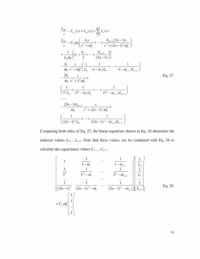
61
−−++
−
×−+
−−
−
−++
−+
×+
−
−++
−+
+−
−+++=
−+−
+++
−
+=−
−−
−
−−
−−
−
−
−
=
112
02
20
220
12
112
112
02
20
220
3
1111020
20
1
1231
00
20
2212
20
21
0
1
10
))12((1
)12(1
)12()12(
)3(1
)3(1
31
33
)1(1
)1(11
1)12(3
1
)12()12(
)()()(
nn
n
nn
nn
n
nL
DC
n
kkLC
DC
LnLn
nssbn
LLL
ssb
LLLssb
snbb
bL
ns
snb
ssb
Cs
I
sIsIsIs
IL
α
ωω
αα
ωω
ααωω
ω
ωωω
Eq. 27
Comparing both sides of Eq. 27, the linear equations shown in Eq. 28 determine the
inductor values L1,…,Ln-1. Note that these values can be combined with Eq. 26 to
calculate the capacitance values C1,…,Cn-1.
=
−−−−−
−−
−−
−−
−
−
1
1
1
1
1
1
)12(1
)12(1
)12(1
31
31
31
11
11
1
20
1
1
0
12
122
12
122
11
ω
αα
αα
αα
L
nn
n
n
C
L
L
L
nnn Eq. 28

62
As an example, consider the task of finding the value of all components of the 2nd-
order square-wave driver for a 1MHz clock and a 100pF load. From Eq. 25, we have
5
09
11
1
1 ==∴
=−
+−
αxxx Eq. 29
Using this value, we can rewrite Eq. 28 as follows.
×=
−
−−
−
11
102
101001
1
531
31
511
1 2
612
1
0
22
π
L
L Eq. 30
By solving these equations, we find inductor values, L0=140.72uH and L1=79.16uH.
Lastly, since Ω12=5ω0
2=1/L1C1, it follows that C1=64pF.
4.4 Voltage-pulse driven pulse-forming network
Even though the CFVPN shown in Figure 37 has an appropriate configuration for
our target applications, two problems preclude the network from being directly
applied as a clock rail driver. First, a DC current source is required to drive the
network that in practice consumes large amounts of power internally, canceling out
the benefits of the CFVPN clock rail driver. Second, the waveform swings between
+V0/2 and –V0/2 as opposed to 0 and +V0 required for driving CMOS clock nets. We
propose a unique solution that overcomes these impediments.
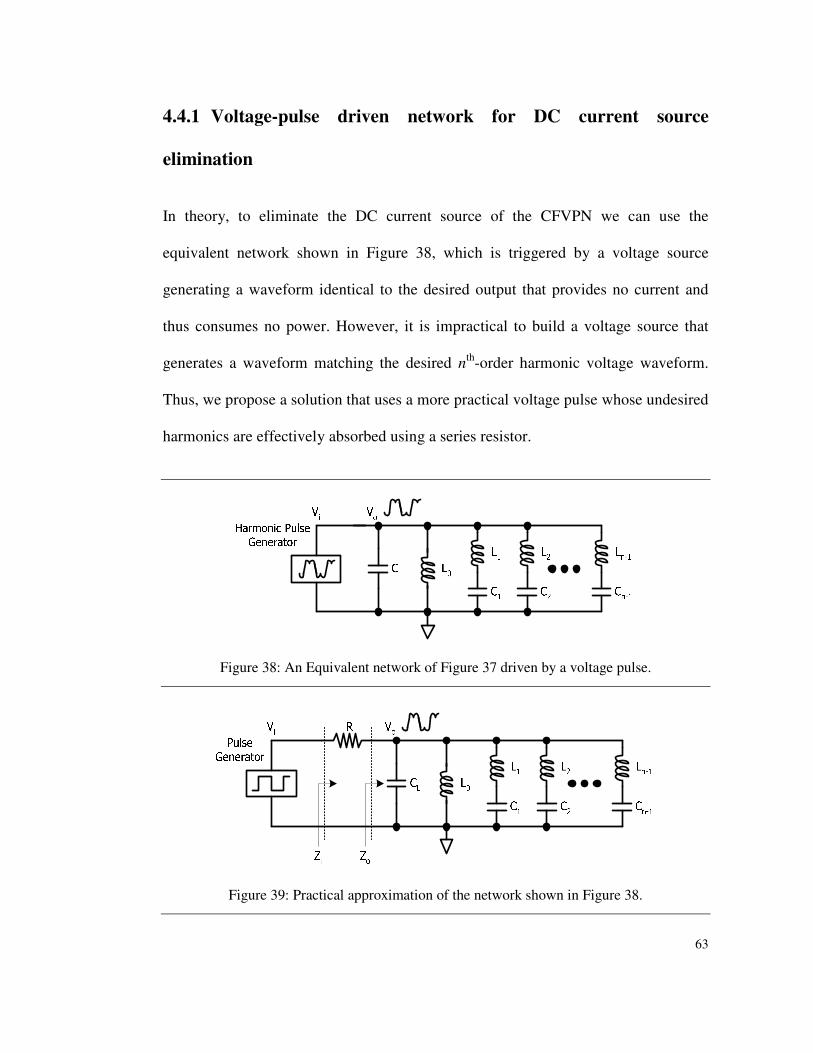
63
4.4.1 Voltage-pulse driven network for DC current source
elimination
In theory, to eliminate the DC current source of the CFVPN we can use the
equivalent network shown in Figure 38, which is triggered by a voltage source
generating a waveform identical to the desired output that provides no current and
thus consumes no power. However, it is impractical to build a voltage source that
generates a waveform matching the desired nth-order harmonic voltage waveform.
Thus, we propose a solution that uses a more practical voltage pulse whose undesired
harmonics are effectively absorbed using a series resistor.
Figure 38: An Equivalent network of Figure 37 driven by a voltage pulse.
Figure 39: Practical approximation of the network shown in Figure 38.

64
The cheapest source of the voltage pulses is a conventional clock oscillator that,
given finite rise and fall times, approximates a trapezoidal wave. The first n
harmonics of the trapezoidal waveform should match that of the network. However,
the trapezoidal-wave clock signal will also contain higher order harmonics than those
generated by the network. This will cause significant current draw from the voltage
source, reducing the power efficiency of the proposed rail driver.
We propose to reject these higher order harmonics from the input pulse generator by
placing a resistor between the input and output of the network as depicted in Figure
39. To understand the benefits of adding this resistor we first write the impedance
function of the original network as follows.
20
22
'12
20
22
'3
20
2
'1
)12/(1
3/1/1)(
ωωω
ωωω
ωωωω
−−+
+−
+−
=
−
nLj
LjLjjZ
n
o
Eq. 31
Note that Eq. 31 is the impedance function of the network shown in Figure 36 that is
the equivalent network of Figure 37. Then, by adding the resistance R, the overall
impedance seen by the input pulse generator is,
20
22
'12
20
22
'3
20
2
'1
)12/(13/1/1
)()(
ωωω
ωωω
ωωω
ωω
−−++
−+
−+=
+=
−
n
LjLjLjR
jZRjZ
n
oi
Eq. 32
The transfer function A(j) of the network, represented as the ratio of impedance
Zi(j) and Zo(j), is as follows:

65
real is where,
)12/(1/1
)12/(1/1
)()(
)()()(
00
0
20
22
'12
20
2
'1
20
22
'12
20
2
'1
zjzR
jz
nLjLj
R
nLjLj
jZjZ
jAjVjV
n
n
i
o
i
o
+=
−−++
−+
−−++
−=
==
−
−
ωωω
ωωω
ωωω
ωωω
ωωω
ωω
Eq. 33
where Zo(j) = jz0(). The magnitude and phase shift of this transfer function can
then be expressed as follows.
)()(
)(
00
20
2
0
jzRjzjA
zR
zjA
+∠−∠=∠+
=
ω
ω Eq. 34
Thus, for all frequencies other than the harmonic frequencies (where z0 is finite), the
magnitude approaches 0 and the phase shift approaches 90º as the value of R
increases. Moreover, the magnitude and phase of the transfer function at each of the
n harmonic frequencies can be calculated as follows:
02/2/)()(
1lim)(
lim)(
20
2
0
0
0
0
0
=−=∞+∠−∞∠=∠
=+
=
+=
∞→
∞→
ππω
ω
ω
jRjjA
zR
zjA
jzRjz
jA
k
zk
zk
Eq. 35
where k=(2k-1)0 for k=1,2,…,n. Thus, the value of R does not affect the phase or
magnitude of any of the generated harmonics. A more detailed analytical proof of
Eq. 35 for the 2nd-order driver example is presented in the Appendix.

66
Figure 40: Frequency response of the network shown in Figure 39 (Vo(s)/Vi(s)).
Figure 41: The proposed network with the parasitic resistance of inductors.
Figure 40 depicts the frequency response of the 2nd-order driver for a 1MHz clock
signal with different resistance values. It clearly shows that no distortion is incurred
at two resonant frequencies (1MHz and 3MHz) for all resistance values. From this
graph, it seems beneficial to increase the resistance to reject higher harmonics.

67
However, the parasitic resistances of the components and wires unfortunately reduce
the voltage level of the output signal as R becomes larger because of the inherent
voltage divider present between the parasitic resistances and R. To understand this
more clearly, the driver is redrawn in Figure 41 with a parasitic DC resistor of each
inductor for the 2nd-order. Other parasitic components whose values are negligible
compared with components used are not considered to simplify the analysis. If we
apply KCL on the output node, we can write the following equation.
)(1
1
)()(
11112
1
00
sVCsRCLs
sCRsL
sC
RsVsV
oL
oi
⋅
+++
++=
−
Eq. 36
By arranging for Vo,
11
)()(
11112
1
00 +++
+++
=
CsRCLssRC
RsLR
sRC
sVsV
L
io
Eq. 37
Figure 42 shows the magnitude and phase of Vi/Vo at the first two harmonic
frequencies. R0=30Ω and R1=25Ω are used for the inductor parasitic resistances, as
specified by the data sheet for the inductor used in our implementation [11]. Though
there is negligible change in the phase, the magnitude decreases from 0.96 to 0.69
when R increases from 1kΩ to 10kΩ. This is in sharp contrast to the ideal network
whose frequency response at the harmonic frequencies is not affected by the
resistance value as demonstrated in Figure 40. Consequently, it is important to use an
adequate resistance value R while maintaining proper voltage levels of the output
signal for low power dissipation. For driving 97.8pF load capacitance at 1MHz, our

68
test measurement demonstrates that only 15% of fCLV2 is dissipated with a 2kΩ
resistance with negligible degradation in output voltage.
(a)
(b)
Figure 42: Frequency response of the network shown in Figure 41 for the first two harmonic frequencies (a) magnitude (b) phase.

69
4.4.2 A tank capacitor for a positive-swing waveform
The output of the network in Figure 39 swings between +V0/2 and –V0/2 because one
branch between the output and ground contains a single inductor L0. To redesign the
network to swing from 0 to +V0 we must introduce a DC offset to the output. We
propose accomplishing this by introducing a DC offset at the pulse generator input
and adding a tank capacitance CT in series with L0.
(a)
(b)
Figure 43: DC steady-state for the network (a) without CT (b) with CT.
To understand how a DC offset from the input pulse generator affects the network,
two circuits that differ only in an existence of CT at the DC steady-state condition are
shown in Figure 43. Without CT, the induced output DC voltage is zero because the

70
output and ground node are shorted by the L0 branch as shown in Figure 43 (a). As a
result, the DC current Voffset/R flows into the network, creating significant unwanted
DC power. For the network shown in Figure 43 (b), the tank capacitance CT
connected to L0 in series induces a matching DC offset voltage at the output node,
eliminating the DC current into the network. Moreover, the introduction of the tank
capacitor has a negligible impact on the overall frequency response of the rail driver.
To see this, notice that the impedance functions for the branches in Figure 43 that
contain L0 can be written as follows.
T
T
T CCL
jCj
LjjZ
LjjZ
ωω
ωωω
ωω11
)(
)(
02
02
01
−=+=
= Eq. 38
Assuming CT is very large, the impedance of Z2(j) is negligibly affected by CT as
follows.
T
T
T
T
T
CLjZjZ
LjC
CLj
CCL
jjZ
0
12
00
20
2
2
1when , )()(
1)(
>>≈
=≈−
=
ωωω
ωω
ωω
ωω Eq. 39
In our lab test, a 10nF off-the-shelf capacitor was sufficient to achieve the desired
DC offset voltage within a 0.8MHz to 15MHz frequency range. The final proposed
voltage-pulse driven positive-swing driver is shown in Figure 44.

71
Figure 44: A voltage-pulse driven harmonic resonant rail driver.
4.5 Measurement
The proposed harmonic resonant square-wave rail drivers containing up to four terms
(i.e. 4th-order) were designed and tested on a wire-wrap board that included tunable
inductors and capacitors. We varied the frequency from 0.8MHz to 15MHz by
setting these components to theoretical values we calculated using Eq. 25 and Eq. 28.
We then tuned each component to achieve minimum measured power dissipation and
compared them with their theoretical value. Testing at higher frequencies was
limited by the test setup and equipments that are available to the authors.
Table 4 summarizes the lab measurement results for various configurations. In most
cases, the measured values of the components are within 7% of the theoretical values.
Deviation between the theoretical and tuned capacitance values is larger than for the
inductors presumably because of the large parasitic capacitances in our wire-
wrapped board. As reported in Table 4, approximately 19% of the calculated
conventional power dissipation fCLV2 was dissipated for the 2nd-order driver at
15MHz to drive 97.8pF load capacitance.

72
Tab
le 4
: M
easu
red
data
of
seco
nd,
thir
d, a
nd f
ourt
h sq
uare
-wav
e ha
rmon
ic r
eson
ant
rail
driv
er f
or v
ario
us c
lock
fre
quen
cies
and
loa
d ca
paci
tanc
es. T
he f
irst
thr
ee r
ows
are
data
for
dri
ving
97.
8pF
load
cap
acita
nce
at d
iffer
ent
cloc
k fr
eque
ncie
s an
d th
e la
st r
ow s
how
s da
ta f
or
diff
eren
t loa
d ca
paci
tanc
es a
t 1M
Hz.
The
oret
ical
and
mea
sure
d va
lues
of e
ach
com
pone
nt a
re a
lso
show
n fo
r com
pari
son.

73
Power dissipation increases as the order of the driver increases. This effect appears
to be due to more parasitic components in the test board. In addition, tuning the
circuit for minimum measured power dissipation is increasingly error prone since
more design variables are involved. Note that as we increase the order of the driver,
we must include additional capacitance such as C1 and C2 for the 2nd-order driver.
However, this doesn’t increase the power dissipation significantly because only a
small fraction of the current is drawn from the input pulse generator. In particular,
the pulse generator needs to provide only a very small current sufficient to
compensate the energy loss due to the parasitics of the components.
Figure 45: Normalized power dissipation (P/fCLV2) and transition time versus resistance R. fCLV2 is the theoretical conventional power dissipation to drive load capacitance CL.
The last row in Table 4 shows the measurement data of the 2nd-order driver for
different load capacitances at 1MHz. Resistance values are reduced to achieve 10%

74
rising and falling times of the total cycle time. Power dissipation is increased by
approximately 7% for this case while rising and falling times are shortened by 3%
from the minimal power dissipation mode. This result suggests that by changing
resistance value, we can control the rising and falling times at the expense of power
dissipation. Figure 45 illustrates the measured power dissipation as we changed the
resistance value R for 1MHz and 100pF. The transition time with 2kΩ resistance was
measured as 110ns which is 11% of the total cycle time. Notice that transition times
in Figure 45 are normalized to this value. At 285Ω, the transition time drops to 50ns
(45%) while the power dissipation increases from 15% to 57.9% of fCLV2.
Figure 46 and Figure 47 show oscilloscope traces of the output signal of the driver
for the 2nd- and 3rd-order harmonics. To see how the output signal is synchronized,
the input pulse is also shown. A FFT-enabled oscilloscope trace for the 4th-order
driver output is presented in Figure 48. The figure shows that only four harmonic
frequencies are present in the output signal. Figure 49 presents the trace of the output
signal of the 2nd-order harmonic driver for 10MHz frequency.

75
Figure 46: A scope trace of output waveform for the 2nd-order driver at 1MHz.
Figure 47: A scope trace of output waveform for the 3rd-order driver at 1MHz.

76
Figure 48: A FFT-enabled scope trace of waveform for the 4th-order driver at 1MHz.
Figure 49: A scope trace of output waveform for the 2nd-order driver at 10MHz.

77
When the driver is directly connected to the clock network, the non-linear
characteristic of the transistors can cause load capacitance variations. To measure
power dissipation as a function of the load capacitance variation, we varied CL from
–30% to +30% of the nominal value while keeping all other components the same.
The power was then measured. The results for a 1MHz clock and a 100pF load
capacitance are plotted in Figure 50.
Figure 50: Normalized power dissipation versus load capacitance (CL). All components except CL are kept same as designed for 100pF CL.
Normalized power dissipation in the graph is the ratio between the measured power
dissipation and fCLV2. Power dissipation at 100pF is minimum because the circuit is
designed to harmonically resonate at this value. No frequency variation was noticed
for this range of capacitances as is expected for any externally-driven driver. Unlike
the self-oscillating rail drivers whose frequency varies proportional to the square root

78
of variations in capacitance [5], this beneficial characteristic of our drivers
significantly increases system stability. For capacitance greater than 130%, however,
significant voltage-level degradation is observed. On the other hand, if we reduce the
load capacitance below 70% of nominal, the power dissipation increases rapidly
because current from the input pulse generator mostly charges the load capacitance
instead of it being charged resonantly.
In addition to the increased power dissipation by the load capacitance variation, the
phase shift between the input pulse and the generated output causes a clock jitter. To
quantify this effect, we measured the delay time of the output with respect to the
input pulse at the Vdd/2 voltage level while varying the load capacitance CL from -
30% to +30% of the nominal value. The measurement result is shown in Figure 51.
Figure 51: Clock jitter versus load capacitance (CL).

79
We observed clock jitter ranging from -47ns to 43ns for 1MHz clock frequency. This
relatively high clock jitter can be compensated by an increased clock cycle time.
Therefore, 5% to 10% performance loss is expected for applications with high load
capacitance variation.
Figure 52: Normalized power dissipation versus clock cycle variation.
Another experiment was carried out to measure power dissipation as a function of
frequency change of the input pulse generator. We varied the frequency of the input
pulse generator (fclk) from -10% to +10% from its nominal value then the power was
measured. Figure 52 shows the measurement results of the power dissipation. At the
nominal frequency (1MHz), the normalized power dissipation is 14% of fCLV2.
When fclk is reduced by 10% from its nominal value, the power dissipation is
increased to 39% of fCLV2. 36% of fCLV2 was measured when fclk is increased by

80
10%. For 2% frequency fluctuation, the power dissipation is increased to 15% of
fCLV2.

81
Chapter 5
CASE STUDY: LOW-POWER FIR FILTER
Now that the low power circuit techniques have been proposed for two major power
consumption components – clock networks and memory blocks - of portable DSP
applications, a low-power FIR filter design is presented in this chapter as one way to
combine these techniques in real DSP applications.
5.1 Motivation
FIR (Finite Impulse Response) filtering is one of the most commonly used functions
in DSP and communication systems [41][44]. Some examples include spectral
shaping, matched filtering, noise rejection, channel equalization, and wavelet
decomposition/reconstructions [44]. Its operation is achieved by convolving input
data samples with the desired impulse response of the filter. The output y[n] of an N-
tap FIR filter (Figure 53) is given by the weighted sum of the latest N input data
samples.
−
=
−⋅=1
0
][][][N
k
knxkhny Eq. 40
The weights h[k] in the above expression are the filter coefficients. The number of
taps (N) and the coefficient values are derived so as to satisfy the desired filter
response in terms of passband ripple and stopband attenuation. The most ubiquitous
hardware implementation for FIR filters is to use a generic DSP architecture as

82
shown in Figure 54 where two memory blocks (coefficient and data) and a multiply-
accumulate (MAC) unit are synchronously reused to mimic a tapped delay line
implementation as shown in Figure 53. Two memory blocks can be accessed
simultaneously. This is similar to the Harvard architecture employed in most
programmable DSP’s [38][68].
Figure 53: A tapped delay line implementation of N-tap FIR filter.
Figure 54: A generic DSP architecture for FIR filter.

83
For an N-tap FIR filter, the latest N data samples are required. Therefore, the latest N
samples need to be stored in the data memory. After every output computation, a
new data sample is read and stored in the data memory, and the oldest data sample is
removed. Data sample x[k] for the current computation becomes data sample x[k-1]
for the next computation. The existing data samples thus need to be shifted by one
position for every output. The power dissipated due to this data movement can be
minimized by using a circular buffer [68] where the pointer to the data is moved
instead of moving the data. For programmable FIR filters, the coefficient memory
can be configured as a circular buffer as well. It is straightforward to design a
circular buffer by combining a conventional SRAM array with an address
sequencing logic, which is often implemented by up/down counters. This approach is
quite wasteful both in power and speed aspects if the accesses to the memories in the
target applications, such as FIR filtering, are all sequential as demonstrated in
Chapter 3. In particular, as N becomes large, the power dissipated by the drivers of
the address lines and decoders grows significantly.
A clock network is another major power consumption source of FIR filter design. In
particular, the number of taps required increases significantly in modern DSP
systems to achieve high overall resolution with relatively simple analog components.
This leads to a high-frequency system clock even if the sampling rate of input and
output data is slow. For example, the sampling rate of typical CD audio signals is
44.1KHz. To design a low-pass filter with the specification of 4.1KHz (20-24.1KHz)
transition band and 80dB stopband attenuation, approximately 120 taps are required

84
[16] thus the system clock frequency has to be increased to 5.92MHz. Because the
system clock is distributed throughout the system (on-chip and off-chip), total power
dissipation of the system significantly grows by the increase of the clock frequency.
An on-chip PLL can be used to multiply the system clock to generate a faster on-chip
clock. However, typical multiplication factors of PLLs ranges from two to five [21].
In addition, the power dissipation of a PLL can easily eclipse the power savings from
reducing the system clock frequency.
This chapter presents a novel FIR filter design where the on-chip clock signal is
locally generated from the self-resetting memory so that the system clock can be kept
at the sample rate. The local clock signal automatically stops as soon as filter
operations are completed. Moreover, by utilizing an existing self-resetting control
signal of a memory block for a local clock signal, there is virtually no circuit
overhead. This is in sharp contrast to conventional techniques such as clock gating
and stoppable clocks. The sequential access memory presented in Chapter 3 is used
for coefficient and data memory blocks to further reduce power dissipation of
memory accesses. Clock distribution network schemes are also discussed to
maximize the power savings benefit of the resonant clock rail driver presented in
Chapter 4.

85
5.2 Architecture
Figure 55 shows a block diagram of our proposed FIR filter. A slow sample clock
(phi) is connected only to I/O registers.
Figure 55: A block diagram of a N-tap FIR filter
A faster operation clock (lphi) is locally generated from the data memory completion
signal and connected to datapath pipeline registers and memories. A typical
implementation includes a clock distribution network on the local clock to reduce
skew and slew rate. The clock frequency of lphi is determined by the latency of the
read accesses. Therefore, the datapath should be designed such that the critical path
86
latency of the datapath is less than the read access latency of the data memory.
However, this constraint can be relaxed by inserting delay lines on the local clock net
to increase the clock cycle arbitrarily. To minimize the power dissipation of
decoding and driving address lines, sequential access memories are used both for
data memory and coefficient memory. To keep track of the number of operations to
be performed, a controller is integrated into the datapath. All other datapath blocks
including I/O registers, a controller and a MAC (multiply-accumulate) are designed
using a standard ASIC design flow under timing constraints taken from the memory
design simulation.
5.3 Timing and circuits
5.3.1 Local clock generation
The most unique feature of the proposed FIR filter is to use the self-resetting signals
from a sequential access memory as a clock signal for datapath blocks. Figure 27 is
redrawn in Figure 56 with the new signal complete. For a synchronous design where
the memory is triggered by the system clock, self-resetting circuit techniques are
mainly used to make a sequence of micro-operations in line so that there is no waste
in power dissipation. Therefore, completion detection is not required as long as a
clock cycle time is longer than the read access latency.

87
Figure 56: A timing diagram of the read operation of SAM with a newly added complete signal.
To enable the memory to trigger read accesses without an external clock, the
complete signal is fed back to the memory clock input port. Both edges of the
complete signal are asserted by the self-resetting circuit operations discussed in
Chapter 2. The local clock signal lphi is simply a delayed signal of complete.
Typically, the phase difference between complete and lphi includes clock tree
insertion delay. All micro-operations of each read access are triggered by the rising
edge of lphi.
5.3.2 Controller
As defined in Eq. 40, every step of FIR filtering starts with read accesses to the data
and coefficient stored in memories and finishes with a MAC operation. The initial
read access can be triggered easily by utilizing a rising edge of the system clock.
However, determining the last access, and thus the completion of operations,

88
requires additional logic. For a 64-tap FIR filter, one 6-bit counter and simple state
machine can implement this function as presented in Figure 57. A timing diagram of
the controller is shown in Figure 58.
Figure 57: A block diagram of the 64-tap FIR filter controller.
Figure 58: A timing diagram of the 64-tap FIR filter controller.
lrenc and lrend are read enable signals for the coefficient memory and data memory
respectively. The pphi signal which is generated at the rising edge of the system
clock phi, resets the counter and asserts lrenc and lrend. The up-counter keeps
incrementing the counter value at each rising edge of lphi. When the counter value

89
cnt reaches 62 and 63, lrenc and lrend are reset to zero respectively. When these
signals are low at the rising edge of lphi, no read access is performed, and lphi stops
toggling thereafter. For each output of FIR filtering, one redundant read access to the
data memory is performed because the starting location of the data memory has to be
incremented by one as shown in Figure 59. Data from this additional access is
discarded and not forwarded to the datapath blocks.
Figure 59: A starting location of the data memory for each sample.
5.3.3 Read operation
We have shown how to generate the local clock signal (lphi) and read enable signals
(lrenc, lrend) in previous subsections. To see how these signals are used for read
operations, a timing diagram for read operations is presented in Figure 60. The initial
read access (x[i-63]) is triggered by the pphi signal when the global read enable (ren)
signal is high. This initial read access then creates the first rising edge of lphi. As
discussed in the previous subsection, the lphi signal repeats toggling until the lrend
signal goes to low. The read controller for the single bank sequential access memory
shown in Figure 26 is slightly modified to trigger the initial read access at the rising

90
edge of pphi. Figure 61 shows the modified circuit diagram for the rseq_en signal.
Other read control signals are not affected by the new timing.
Figure 60: A timing diagram of read accesses for the 64-tap FIR filter.
Figure 61: A modified read controller of the SAM to enable an initial read access by pphi

91
For a multi-bank sequential access memory, only one of the banks is active for a
given cycle. Consequently the complete signal from the active bank toggles while
others are held high. Therefore, all of these signals are combined by an AND gate to
get the local clock signal that repeats toggling during the whole operation. A block
diagram of the four-bank example and its timing diagram are depicted in Figure 62
and Figure 63. To simplify the timing diagram, each bank is assumed to have two
rows.
Figure 62: A block diagram of the data memory to generate the local clock signal lphi.

92
Figure 63: A timing diagram of Figure 62. Each bank is assumed to have only two rows to simplify the diagram.
The start address of read accesses can reside in any of the banks for a given sample.
The read controller for a single bank sequential access memory shown in Figure 61
must be modified because all of the banks will be triggered by the pphi signal
otherwise. Note that the bank location of the start address at the beginning of the
operations is stored in the bank_enq signal of Figure 24. By adding one NMOS
transistor with a gate connected to bank_enq in the newly added NMOS stack of
Figure 61, the initial triggering of read accesses can be easily achieved. Figure 64
shows the modified circuit diagram of the read controller for the multi-bank
sequential access memory.

93
Figure 64: A modified read controller of the multi-bank SAM to enable an initial read access by pphi.
5.3.4 Write operation
Regardless of the tap size of a FIR filter, only one write operation for the data
memory is required per sample. A sequential access memory for FIR filtering is
basically the same as a FIFO configuration. Therefore, the oldest sample stored in
the data memory during the previous period is replaced with the new sample at the

94
beginning of the current period. Concurrent read and write to/from the same location
usually requires additional bypassing logic or a prolonged latency. To avoid this
overhead, read accesses start from the oldest sample to the new sample whereas the
new data is written into the data memory at the beginning of the current period. The
pphi signal is used to trigger the write operation as shown in Figure 65.
Figure 65: A timing diagram of write operations.
5.3.5 Overall timing for FIR filtering
An overall timing diagram of FIR filtering is shown in Figure 66. Multiplier inputs
(m1/m2) and the accumulator output (acc) are pipeline register outputs triggered by
the lphi signal. The FIR filter output (FIRout) is latched by the I/O registers at the
subsequent rising edge of phi. coef and data are outputs of the coefficient memory
and the data memory, respectively. Note that the final value of the accumulator is
available at the last rising edge of lphi.

95
Figure 66: An overall timing diagram of FIR filtering

96
5.4 Issues with the clock distribution network
The clock network is one of the major sources of power dissipation in DSP
applications. In particular, capacitances associated with the clock network at the
system level are typically higher than on-chip clock networks. Therefore, by
reducing the system clock frequency from the operating rate to the sample rate, a
significant amount of energy can be saved. The resonant clock rail driver presented
in Chapter 4 can save energy even further by driving the clock network resonantly.
In addition, it has been demonstrated that energy efficiency of the resonant clock rail
driver increases as clock frequency decreases.
In this section, we will present issues related with the clock distribution network to
minimize clock power dissipation.
5.4.1 Global and hierarchical clock trees
Since the clock signal to trigger operations for each FIR filter is locally generated
from the memory, it is inherent to use hierarchical clock tree generation. For each
FIR filter, a small clock tree whose root is the complete signal of the data memory is
generated to meet timing requirements such as clock skew and transition time. At a
chip level, another clock tree is inserted to minimize clock skew from the system
clock node to each leaf node, which is the system clock input of the FIR filter. A
hierarchical clock tree scheme is depicted in Figure 67.

97
Figure 67: Hierarchical clock tree generation for FIR filter banks.
One of the advantages of this configuration is the small leaf node capacitance of the
system clock. Clock trees of high-speed clocks are localized in each block so that
clock tree overhead is smaller as compared with a global clock tree generation.
(Figure 68) Contrary to conventional approaches in which a high-speed clock is
distributed across a whole chip, there is no timing relationship between these local
clock signals. Therefore, the clock tree overhead to minimize clock skew and clock
slew rate can be significantly reduced.

98
Figure 68: Conventional clock tree generation with global clock distribution.
5.4.2 Resonant and conventional clock drivers
To ensure fast clock transitions in conventional systems, buffers are inserted to drive
large load capacitances of a clock net [13][20]. There are two common clock driving
schemes: single driver and distributed buffer [57]. In the single driver scheme as
shown in Figure 69 (a), a chain of cascaded buffers with a very large buffer at the
end is used at the clock source, and no buffers are used elsewhere; in the distributed
buffers scheme as shown in Figure 69 (b), intermediate buffers are inserted in
various parts of the clock tree. The single driver scheme has the advantage of
avoiding adjustment of intermediate buffer delays as in the distributed buffers
scheme. Often in conjunction with this scheme, wire sizing is used to reduce the
clock phase delay. Widening the branches that are close to the clock source can also

99
reduce skew caused by asymmetric clock tree loads and wire width deviations
[75][55]. The distributed buffers scheme is often preferred over the single buffer
scheme as the chip size increases due to its flexibility and small clock phase delay
[19][13]. For power minimization in a clock tree, the distributed buffers scheme is
also preferred due to its capability to shut down subsystems by replacing buffers with
logic gates.
(a) (b)
Figure 69: Two clock tree driving scheme: (a) Single driver scheme (b) distributed buffer scheme
The resonant clock rail driver works in a similar way as the single driver scheme.
The clock driver can drive any arbitrary capacitance for a given slew rate and total
load capacitance during the design procedure. Therefore, no intermediate clock
buffer is needed. To reduce RC delay resulting from the relatively long wire length
from a clock pin to leaf nodes, clock wires can be expanded at the expense of
increased load capacitances. However, the cost is considerably smaller than a
conventional single driver scheme because of the high energy efficiency of the

100
resonant clock rail driver. Considering the slow clock frequency requirement and
hierarchical clock tree configuration of the proposed design, the resonant clock rail
driver can be easily applied. In addition, shutting down subsystems such as FIR filter
banks is controlled by control signals rather than gated clock signals. When the read
enable signal is not asserted, read accesses to the data memory is not triggered, and
thus the local clock signal is automatically disabled.
Figure 70: Serpentine clock distribution network.
Figure 71: Balanced H-tree clock distribution network.
Several clock routing topologies can be applied for the resonant clock rail drivers.
Figure 70 shows one possible topology where each load is driven by a single point-
to-point wire and lengths are matched using a serpentine structure [27]. This

101
structure is relatively simple to design and has virtually zero skew for identical loads
as long as coupling capacitances are insignificant. A symmetric H-tree [15][25]
shown in Figure 71 has much smaller clock capacitances than the serpentine
structure with a negligible clock skew for ideal load distribution. However, tuning
tree topologies to drive highly non-uniform loads with low skew can be much more
difficult.

102
5.5 Implementation
Two prototype 16-b FIR filters - 64-tap and 16-tap - were designed and implemented
in the TSMC 0.25-µm n-well CMOS process. A standard ASIC design flow was
generally applied to generate datapath blocks including MACs and controllers using
a standard-cell library from Artisan. A timing constraint for the datapath blocks was
set to 4.0ns at 2.5V to meet the read access latency of the memory. A Wallace tree
multiplier and carry lookahead adder structures are used for MACs. The 16-tab and
64-tab FIR filters occupy 329.6-µm x 496.1-µm and 395.4-µm x 848.5-µm,
respectively. Table 5 summarizes the characteristics of the prototype FIR filters.
Layout plots for the two FIR filters are presented in Figure 72 and Figure 73.
Table 5: Summary of the process technology and the test chip
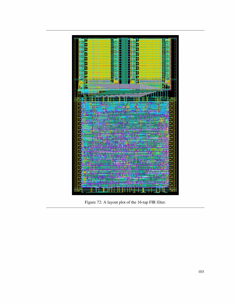
103
Figure 72: A layout plot of the 16-tap FIR filter.

104
Figure 73: A layout plot of the 64-tap FIR filter.

105
5.6 Kaiser-window low-pass FIR filter
Simple low-pass FIR filters based on the Kaiser-window method [53] were designed
using Matlab software [67]. Figure 74 shows the frequency response of the designed
filters. Real 16-bit human speech signal sampled at 16KHz is used for input and
filtered to produce output. 2048-point FFT plots for both input and output signals are
shown in Figure 75. It is clearly shown that the high frequency components are
filtered out.
0 0.1 0.2 0.3 0.4 0.5 0.6 0.7 0.8 0.9 1-2000
-1500
-1000
-500
0
Normalized Frequency (×π rad/sample)
Pha
se (d
egre
es)
0 0.1 0.2 0.3 0.4 0.5 0.6 0.7 0.8 0.9 1-150
-100
-50
0
50
Normalized Frequency (×π rad/sample)
Mag
nitu
de (d
B)
16-tap FIR64-tap FIR
16-tap FIR64-tap FIR
Figure 74: Frequency response of two low-pass FIR filters.

106
0 1 2 3 4 5 6 7 8-120
-100
-80
-60
-40
-20
0
Freq (KHz)
Mag
nitu
de (d
B)
Original64-tap filtered16-tap filtered
Figure 75: FFT plot of the speech sampled at 16KHz
5.7 Simulation results
Circuits are extracted from layout and verified using Mentor Graphics Calibre suite.
Then Nanosim simulation was performed to measure power dissipation and
performance. The speech signal shown in Figure 75 was used for input, and the
result was compared with Matlab simulation output.
To measure the performance of the proposed FIR filter, the cycle time of the local
clock signal lphi was measured. Figure 76 shows the average value of the cycle time
for four supply voltages. As discussed in Chapter 3, there is no decoding time
involved for sequential access memories. Therefore, the cycle time difference

107
between the two FIR filter configurations is measured to be less than 7% for all
occasions. This small difference mainly results from the 4-input AND gate (Figure
62) to combine complete signals from each bank and relatively longer wires from the
memory to the datapath for a 64-tap FIR filter.
0.8 1 1.2 1.4 1.6 1.8 2 2.2 2.4 2.6
1
5
10
15
20
25
Vdd
Tcy
cle
(ns)
16-tap FIR64-tap FIR23.69
22.13
8.44
5.49
4.37
9.07
5.89
4.65
Figure 76: Average cycle time of two FIR filters.
In addition to the average cycle time of the lphi signal, each cycle time was
measured to observe cycle time variation. Table 6 summarizes the cycle time
variation results. Variation from the average values ranges from -2.12% to 1.98%,
which can be easily compensated by giving 3% - 5% more timing margin when the
datapath is designed.

108
Table 6: Clock cycle time variation = (Tmax/min – Tavg) / Tavg
Figure 77 shows the power dissipation of two FIR filters for different supply
voltages. The number of operations per sample is 64 and 16 for the 64-tap FIR filter
and the 16-tap FIR filter, respectively. Energy per sample of the 64-tap FIR filter is
approximately 3.9 times more than that of the 16-tap FIR filter, which mainly results
from the increase in required number of operations.
1 1.5 2 2.50
2
4
6
8
10
12
14
16
18
Vdd
Ene
rgy/
Sam
ple
(nJ)
16-tap FIR64-tap FIR
3.9x
Figure 77: Energy/sample plot for two FIR filters.

109
Figure 78 shows the simulation results of the power breakdown of the two FIR filters
with VDD=1.0V and 16.0KHz sample rate. Clock trees consume only 4.16 - 6.80% of
total power dissipation because high-speed operating clocks are generated only
locally, without a connection to any off-chip system clock pin or the use of a PLL.
Power dissipation of the memories for the 64-tap FIR filter is about six times
(intuitively expected to be four fold) that of the 16-tap FIR filter mostly due to longer
routing wires from the memories to the datapath blocks and data dependency of the
power dissipation.
0
5
10
15
20
25
30
Pow
er (u
W)
Datapath (MAC, Registers, etc)Data & Coef MemoriesClock Tree
16-tap FIR 64-tap FIR
7.04(83.90%)
1.00(11.94%) 0.35
(4.16%)
24.77(74.91%)
6.05(18.29%)
2.25(6.80%)
Figure 78: Power breakdown of two FIR filters.
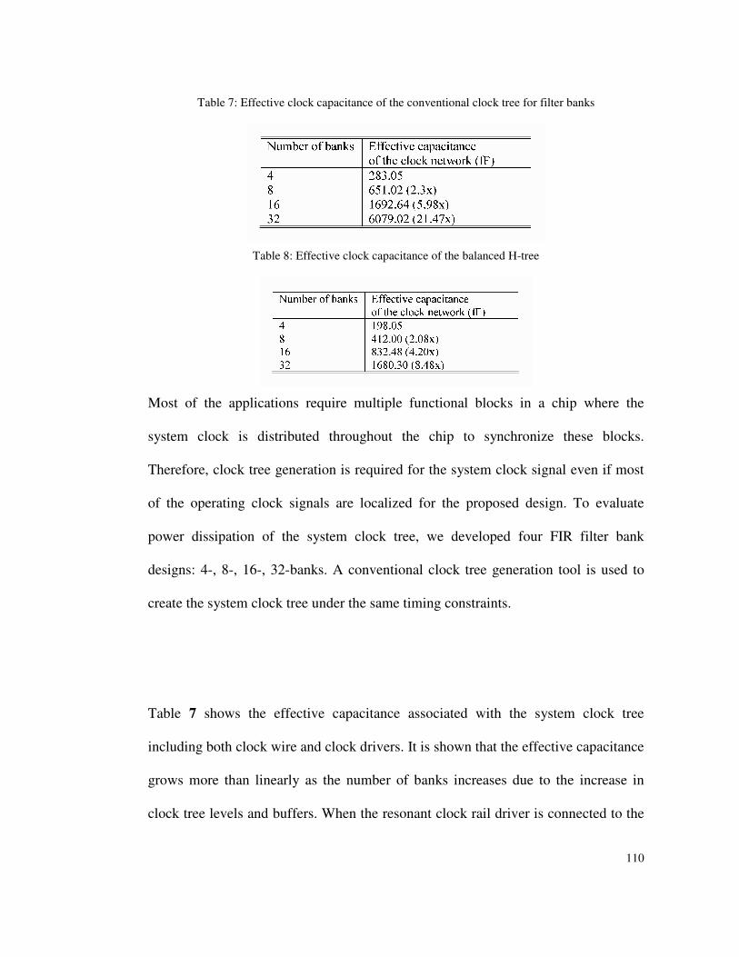
110
Table 7: Effective clock capacitance of the conventional clock tree for filter banks
Table 8: Effective clock capacitance of the balanced H-tree
Most of the applications require multiple functional blocks in a chip where the
system clock is distributed throughout the chip to synchronize these blocks.
Therefore, clock tree generation is required for the system clock signal even if most
of the operating clock signals are localized for the proposed design. To evaluate
power dissipation of the system clock tree, we developed four FIR filter bank
designs: 4-, 8-, 16-, 32-banks. A conventional clock tree generation tool is used to
create the system clock tree under the same timing constraints.
Table 7 shows the effective capacitance associated with the system clock tree
including both clock wire and clock drivers. It is shown that the effective capacitance
grows more than linearly as the number of banks increases due to the increase in
clock tree levels and buffers. When the resonant clock rail driver is connected to the

111
system clock, serpentine or symmetric H-tree clock distribution networks can be
used. Table 8 shows the system clock capacitance when the symmetric H-tree clock
distribution network is used. Contrary to the conventional clock distribution network,
capacitance increases linearly. Assuming the energy efficiency of the resonant clock
rail driver is 80%, approximately 94.5% (1680.30*0.2/6079.02=0.055) energy
savings results for a 32-bank case.
When the system clock frequency is low, such as that of the FIR filter design
proposed in this chapter, the power savings in the on-chip clock distribution network
is relatively small by applying the resonant clock rail driver. However, if an
application requires a system clock at the operating rate or a large system clock
network capacitance, clock power dissipation can be greatly reduced by driving most
on-chip and off-chip clock networks resonantly. In addition, moving the global clock
off the chip will improve the reliability of a system [26] because the crosstalk
between logic gates and intermediate clock buffers and the di/dt noise at clock edges
by the clock buffers can be considerably eliminated. Note that the resonant clock rail
driver is orthogonal to other low-power techniques. As the resonant clock rail driver
is applied only on the clock network, all other conventional low-power circuit
techniques can be easily combined.

112
Chapter 6
CONCLUSIONS
In this dissertation, we presented various circuit solutions to reduce power
dissipation in the memory blocks and the clock network, which are two components
that account for a significant amount of power dissipation in portable DSP
applications.
First, a novel low-power register file and a sequential access memory have been
designed, fabricated, and tested. The register file provides wide voltage scalability
and various clocking support. A novel read controller based on a self-resetting
postcharge logic minimizes the static power dissipation. The sequential access
memory design demonstrates the unique feature of having power dissipation that is
largely independent of memory size by replacing decoders, an address sequencing
logic, and address line drivers with the sequencer logic. The proposed design
demonstrates the low-power potential of sequential access memories for applications
requiring non-random access patterns.
Second, we presented a new algorithm and a prototype implementation of a
harmonic resonant rail driver. The design goal is to produce an energy-efficient
harmonic resonant clock signal using a simple network topology requiring no
additional DC power supply. The experiment result shows that a significant amount

113
of energy for driving the clock load can be recycled and saved by the resonant
characteristic of the proposed driver. Depending on the number of harmonics in the
driver, we were able to save 70-85% of the conventional power dissipation.
Moreover, the frequency variation caused by changes in load capacitance
demonstrated significant improvement from the previously reported resonant clock
drivers.
Third, a novel FIR filter was designed and tested to demonstrate the feasibility of the
proposed circuit techniques in a real DSP application. A self-resetting data memory
is configured such that it generates a stoppable clock, which is synchronously started
and asynchronously stopped. In this way, we were able to reduce the system clock
frequency to the sample rate. The resonant clock rail driver can be easily combined
to further reduce power dissipation of the system clock network.
As the proposed FIR filter can detect the completion of operations and shut down the
local clock automatically, it is possible to reduce significant leakage currents when
combined with leakage current reduction techniques such as back-bias and dynamic
voltage scaling. One of the advantages of the proposed design is the ability for
subcomponents to go to the sleep state as soon as the operations are completed even
during the operating mode. For a moderate speed requirement, as is often the case for
portable battery-powered DSP applications, a self-resetting memory can be
configured as the cheap clock source.

114
On-chip implementation of the resonant clock driver will improve power efficiency
and the frequency of the output clock. Quantization of variations on energy
efficiency and phase shift by driving non-linear capacitances such as MOS gate
capacitances will be necessary to produce a desired waveform.

115
References
[1] B. Ackland, “The role of VLSI in multimedia”, IEEE Journal of Solid-State Circuits, Vol. 29, No. 4, Apr. 1994, pp. 381-388
[2] M. Alidina, J. Moteiro, S. Devadas, A. Ghosh, M. Papaefthymiou, “Precomputation-based sequential logic optimization for low power”, IEEE Transactions on VLSI Systems, Vol. 2, No. 4, Jun. 1994, pp. 426-436
[3] A. Alvandpour, R. Krishnamurthy, K. Soumyanath, S. Borkar, “A low-leakage dynamic multi-ported register file in 0.13-µm CMOS”, International Symposium on Low Power Electronics and Design, pp. 68-71, 2001
[4] B. Amrutur, M. Horowitz, “A replica technique for wordline and sense control in low-power SRAM’s”, IEEE Journal of Solid-State Circuits, Vol. 33, No. 8, Aug. 1998, pp. 1208-1219
[5] B. Arbetter, R. Erickson, D. Maksimovic, “DC-DC converter design for battery-operated systems”, 26th Annual IEEE Power Electronics Specialists Conference, Vol. 1, pp. 103-109, 1995
[6] W. Athas, L. Svensson, J. Koller, N. Tzartzanis, E Ying-Chin Chou, “Low-power digital systems based on adiabatic-switching principles”, IEEE Transactions on VLSI Systems., Vol. 2, No. 4, Jun. 1994, pp. 389-407
[7] W. Athas, L. Svensson, N. Tzartzanis, “A resonant signal driver for two-phase, almost-non-overlapping clocks”, Proceedings of International Symposium on Circuits and Systems, Vol. 4, pp. 129-132, 1996
[8] W. Athas, N. Tzartzanis, L. Svensson, L. Peterson, “A low-power microprocessor based on resonant energy”, IEEE Journal of Solid-State Circuits, Vol. 32, No. 11, Nov. 1997, pp. 1693-1701
[9] W. Athas, N. Tzartzanis, W. Mao, L. Peterson, R. Lal, K. Chong, J. Moon, L. Svensson, M. Bolotski, “The design and implementation of a low-power clock-powered microprocessor”, IEEE Journal of Solid-State Circuits, Vol. 35, No. 11, Apr. 2000, pp. 1561-1570, Apr. 2000
[10] W. Athas, W. Liu, J. Svensson, “Energy-recovery CMOS for highly pipelined DSP designs”, International Symposium on Low Power Electronics and Design, pp. 101-104, 1996

116
[11] N. August, D. Ha, “On the low-power design of DCT and IDCT for low bit-rate video codecs”, Proceedings of the 14th Annual IEEE International ASIC/SOC Conference, pp. 203-207, 2001
[12] B. Baas, “A low-power, high-performance, 1024-point FFT processor”, IEEE Journal of Solid-State Circuits, Vol. 34, No. 3, Mar 1999, pp. 380-387
[13] H. Bakoglu, Circuits, Interconnections, and Packaging for VLSI, Addison-Wesley Publishing Company, 1987
[14] L. Benini, P. Siegel, G. De Micheli, “Saving power by synthesizing gated clocks for sequential circuits”, IEEE Design and Test of Computers, Vol. 11, No. 4, pp. 32-41, Winter 1994
[15] K. Bernstein, K. Carrig, C. Durham, P. Hansen, D. Hogenmiller, E. Nowak, N. Rohrer, High speed CMOS design style, Kluwer Academic Publisher, 1998
[16] B. Brandt, B. Wooley, “A low-power, area-efficient digital filter for decimation and interpolation”, IEEE Journal of Solid-State Circuits, Vol. 29, No. 6, Jun. 1994, pp. 679-687
[17] A. Chandrakasan, R. Brodersen ed., Low power digital CMOS design, Kluwer Academic Publishers, 1995
[18] A. Chandrakasan, R. Brodersen, “Minimizing power consumption in digital CMOS circuits”, Proceedings of the IEEE, Vol. 83, No. 4, Apr 1995, pp. 498-523
[19] S. Dhar, M. A. Franklin, D. F. Wann, “Reduction of clock delays in VLSI structures”, Digest of Technical Papers of 1984 IEEE/ACM International Conference on Computer-Aided Design, pp. 778-783, 1984
[20] D. Dobberpuhl, R. Witek, R. Allmon, R. Anglin, D. Bertucci, S. Britton, L. Chao, R. Conrad, D. Dever, B. Gieseke, S. Hassoun, G. Hoeppner, K. Kuchler, M. Ladd, B. Leary, L. Madden, E. McLellan, D. Meyer, J. Montanaro, “A 200MHz 64-b dual-issue CMOS microprocessor”, IEEE Journal of Solid-State Circuits, Vol. 27, No. 11, Nov. 1992, pp. 1555-1567
[21] D. Duarte, Clock network and phase-locked loop power estimation and experimentation, Ph.D. Thesis, Electrical Engineering Dept., Pennsylvania State University
[22] J. Eager, “Advances in rechargeable batteries pace portable computer growth”, Proceedings of the Silicon Valley Personal Computer Conference, pp. 693-697, 1991

117
[23] M. Ferretti, P. Beerel, “Low swing signaling using a dynamic diode-connected driver”, Proceedings of the 27th European Solid-State Circuits Conference, 2001
[24] R. Franch, J. Ji, C. Chen, “A 640-ps, 0.25-µm CMOS, 16 x 64-b three-port register file”, IEEE Journal of Solid-State Circuits, Vol. 32, No. 8, Aug. 1997, pp. 1288-1292, Aug. 1997
[25] E. Friedman ed., Clock Distribution networks in VLSI circuits and systems, IEEE Press, 1995
[26] R. Frye, “Physical scaling and interconnection delay in multichip modules”, IEEE Transactions on Components, Packaging, and Manufacturing Technology, Vol. 17, No. 1, Feb. 1994, pp.30-37
[27] G. Geannopoulos, X. Dai, “An adaptive digital deskewing circuit for clock distribution networks’, Digest of Technical Papers of 45th International Solid-State Circuits Conference, pp. 400-401, 1998
[28] G. Glasoe, and J. Lebacqz (Eds), Pulse Generator, McGraw-Hill, 1948, pp. 175-224
[29] G. Goertzel, “An algorithm for the evaluation of finite trigonometric series”, American Mathematics Monthly, Vol. 65, No. 1, pp. 34-35, 1968
[30] M. Golden and H. Partovi, “A 500 MHz, write-bypasswd, 88-entry, 90-bit register file”, Digest of Technical Papers of 1999 Symposium on VLSI Circuits, pp. 105-108, 1999
[31] S. He, M. Torkelson, “Design and implementation of a 1024-point pipeline FFT processor”, Proceedings of IEEE 1998 Custom Integrated Circuits Conference, pp. 131-134, 1998
[32] W. Hwang, R. Joshi, and W. Henkels, “A 500-MHz, 32-word x 64-bit, eight-port self-resetting CMOS register file”, IEEE Journal of Solid-State Circuits, Vol. 34, No. 1, Jan. 1999, pp. 56-67
[33] S. Iman, M. Pedram, “Multi-level network optimization for low power”, Proceedings of IEEE/ACM International Conference of Computer Aided Design, pp. 372-377, 1994
[34] K. Itoh, A. Fridi, A. Bellaouar, M. Elmasry, “A Deep sub-V, single power-supply SRAM cell with multi-VT, boosted storage node and dynamic load”, Digest of Technical Papers of 1996 Symposium on VLSI Circuits, pp. 132-133, 1996

118
[35] H. Kawaguchi, Y. Itaka, T. Sakurai, “Dynamic Leakage Cut-off Scheme for Low-Voltage SRAM's”, Digest of Technical Papers of 1998 Symposium on VLSI Circuits, pp. 140-141, 1998
[36] M Khellah, M. Elmasry, “A low-power high-performance current-mode multiport SRAM”, IEEE Transactions on VLSI Systems, Vol. 9, No. 5, Oct. 2001, pp. 590-598
[37] R. Krishnamurthy, A. Alvandpour, G. Balamurugan, N. Shanbhag, K. Souryanath, S. Borkar, “A 130-nm 6GHz 256x32bit leakage-tolerant register file”, IEEE Journal of Solid-State Circuits, Vol. 37, No. 5, May 2002, pp. 624-63
[38] E. Lee, “Programmable DSP architectures: Part I”, IEEE ASSP Magazine, pp. 4-19, Oct. 1988
[39] G. Masera, G. Piccinini, M. Roch, M. Zamboni, “VLSI architectures for turbo codes”, IEEE Transactions on VLSI Systems, vol. 7, No. 3, Sep. 1999, pp. 369-379
[40] C. Mead, L. Conway, Introduction to VLSI systems, Addison Wesley, 1979
[41] M. Mehendale, S. Sherlekar, G. Venkatesh, “Low-power realization of FIR filters on programmable DSP’s”, IEEE Transactions on VLSI Systems, Vol. 6, No. 4, Dec. 1998, pp. 546-553
[42] J. Montanaro, R. Witek, K. Anne, A. Black, E. Cooper, D. Dobberpuhl, P. Donahue, J. Eno, W. Hoeppner, D. Kruckemyer, T. Lee, P. Lin, L. Madden, D. Murray, M. Pearce, S. Santhanam, K. Snyder, R. Stehpany, S. Thierauf, “A 160-MHz, 32-b, 0.5-W CMOS RISC microprocessor”, IEEE Journal of Solid-State Circuits, Vol. 31, No. 11, Nov. 1996, pp. 1703-1714
[43] J. Moon, “Design and analysis of register file”, Directed Research Report (unpublished), 1998
[44] C. Nicol, P. Larsson, K. Azadet, J. O’Neill, “A low-power 128-tap digital adaptive equalizer for broadband modems”, IEEE Journal of Solid-State Circuits, Vol. 32, No. 11, Nov. 1997pp. 1777-1789
[45] L. Nielsen, J. Sparsø, “Designing asynchronous circuits for low power: an IFIR filter bank for a digital hearing aid”, Proceedings of the IEEE, Vol. 87, No. 2, Feb. 1999, pp. 268-281
[46] M. Nomura, M. Yamashina, K. Suzuki, M. Izumikawa, H. Igura, H. Abiko, K. Okabe, A. Ono, T. Nakayama, H. Yamada, “A 500-MHz, 0.4-µm CMOS, 32-

119
word by 32-bit 3-port register file”, Proceedings of the IEEE 1995 Custom Integrated Circuits Conference, pp. 151-154, 1995
[47] K. Osada, J. Shin, M. Khan, Y. Liou, K. Wang, K. Shoji, K. Kuroda, S. Ikeda, K. Ishibashi, “Universal-Vdd 0.65-2.0-V 32-kB cache using a voltage-adapted timing-generation scheme and a lithographically symmetrical cell”, IEEE Journal of Solid-State Circuits, Vol. 36, No. 11, Nov. 2001, pp. 1738-1744
[48] C. Papachristou, M. Nourani, M. Spining, “A multiple clocking scheme for low-power RTL design”, IEEE Transactions on VLSI Systems, Vol. 7, No. 2, Jun. 1999, pp. 266-276, Jun. 1999
[49] K. Parhi, “Algorithm transformation techniques for concurrent processors”, Proceedings of the IEEE, Vol. 77, No. 12, Dec. 1989, pp. 1879-1895
[50] K. Parhi, “Approaches to low-power implementations of DSP systems”, IEEE Transactions on Circuits and Systems-Part I, Vol. 48, No. 10, Oct. 2001, pp. 1214-1224
[51] M. Pedram, “Design Technologies for low power VLSI”, Encyclopedia of Computer Science and Technology, Marcel Dekker Inc., pp. 73-96, 1997
[52] M. Pedram, Q. Wu, “Battery-powered digital CMOS design”, IEEE Transactions on VLSI Systems, Vol. 10, No. 5, Oct. 2002, pp. 601-607
[53] B. Porat, A course in digital signal processing, John Wiley & Sons, Inc., 1997
[54] M. Potkonjak, J. Rabaey, “Maximally and arbitrarily fast implementation of linear and feedback linear computations”, IEEE Transactions on Computer-Aided Design of Integrated Circuits and Systems, Vol. 19, No. 1, Jan. 2000, pp. 30-43
[55] S. Pullela, N. Menezes, J. Omar, L. Pillage, “Skew and delay optimization for reliable buffered clock trees”, Digest of Technical Papers of 1993 IEEE/ACM International Conference on Computer-Aided Design, pp. 556-562, 1993
[56] J. Rabaey, Digital Integrated Circuits: A Design Perspective, Prentice-Hall, 1995
[57] J. Rabaey, M. Pedram ed., Low power design methodologies, Kluwer Academic Publishers, 1996
[58] H. Sahabi, A. Basu, M. Fiala, “VLSI implementation of variable resolution image compression”, Proceedings of the 8th International Conference on VLSI Design, pp. 214-219, 1995

120
[59] W. Shiue, C. Chakrabarti, “Memory exploration for low power, embedded systems”, Proceedings of the 36th ACM/IEEE Design Automation Conference, pp. 140-145, 1999
[60] S. Singh, P. Thiennviboon, R. Ozdag, S. Tugsinavisut, P. Beerel, K. Chugg, “Algorithm and circuit co-design for a low-power sequential decoder,'' Conference record of the 33rd Asilomar Conference on Signals, Systems, and Computers, vol. 1, pp. 389-394, 1999
[61] A. Srivastava, W. Athas, J. Moon, “Timing generator for low power, high-speed SRAMs using postcharge logic”, ACMOS technical report (unpublished), 1999
[62] A. Stratakos, S. Sanders, R. Brodersen, “A low-voltage CMOS DC-DC converter for a portable battery-operated system”, Proceedings of the 25th Annual IEEE Power Electronics Specialists Conf., Vol. 1, pp. 619-626, 1994
[63] C. Su, C. Tsui, A. Despain, “Low power architecture design and compilation techniques for high-performance processors”, Digest of Papers of ’94 Compcon, pp. 489-498, 1994
[64] R. Swanson, J. Meindl, “Ion-implanted complementary MOS transistors in low-voltage circuits”, IEEE Journal of Solid-State Circuits, Vol. 7, No. 2, Apr. 1972, pp. 146-153
[65] C. Tsui, M. Pedram, C. Chen, A. Despain, “Low power state assignment targeting two- and multi-level logic implementations”, Proceedings of IEEE/ACM International Conference Computer Aided Design, pp. 82-87, 1994
[66] N. Tzartzanis, Energy-recovery technique for CMOS microprocessor Design, Ph.D. Thesis, EE-Systems Dept., University of Southern California, Aug. 1998
[67] Matlab User’s Guide, Mathworks Inc., 2002
[68] TMS320C2x/C5x User’s Guide, Texas Instruments, 1993
[69] M.E. Van Valkenburg, Network Analysis 3rd Ed., Prentice-Hall, 1974
[70] Q. Wu, M. Pedram, X. Wu, “Clock-gating and its application to low power design of sequential circuits”, IEEE Transactions on Circuits and Systems-Part I, Vol. 47, No. 3, Mar. 2000, pp. 415-420
[71] T. Xanthopoulos, A. Chandrakasan, “A low-power DCT core using adaptive bitwidth and arithmetic activity exploiting signall correlations and quantization”, IEEE Journal of Solid-State Circuits, Vol. 35, No. 5, May 2000pp. 740-750

121
[72] C. Yeh, C. Chang, J. Wang, “Technology mapping for low power”, Proceedings of the ASP-DAC ’99, Vol. 1, pp. 145-148, 1999
[73] S. Younis, T.F. Knight, “Non-dissipative rail drivers for adiabatic circuits”, Proceedings of the 16th Conference on Advanced Research in VLSI, pp. 404-414, 1995
[74] H. Zhang, V. George, J. Rabaey, “Low-swing on-chip signaling techniques: effectiveness and robustness”, IEEE Transactions on VLSI Systems, Vol. 8, No. 3, Jun. 2000pp. 264-272
[75] Q. Zhu, W. Dai, J. Xi, “Optimal sizing of high speed clock networks based on distributed RC and transmission line models”, Digest of Technical Papers of 1993 IEEE/ACM International Conference on Computer-Aided Design, pp. 628-633, 1993

122
Appendix
PROOF OF EQ. 35 FOR THE 2ND-ORDER DRIVER
By applying KCL on the output node of Figure 39 (for the 2nd-order driver), we can
write the following equation.
)(1
1)()(
112
1
0
sVCLs
sCsL
sCR
sVsVoL
oi ⋅
+++=
− Eq. 41
Vo can be rewritten as follows.
( )
11011
2
1011
34
11
3
02
101103
1104
110
03
110
1111
)(
)()(
)(
CCLLCCRLs
sCLCLCLRC
ss
RCsV
CLs
s
RsLsCLCLCLRsCLLsCCLRL
sVsLsCLL
sV
LLLLL
L
i
LL
i
o
++
++++
⋅
+
=
++++++⋅+
=
Eq. 42
For the 2nd-order square-wave driver, all of the components can be represented with
CL and 0 as follows.
40
110
20
1011
20
1
20
0
20
11
120
120
0
91
,10111
5161
,591
,51
2516
,1
165
,1
95
ωω
ωωω
ωω
==
++∴
===
===
CCLLCLCLCL
CLCLCL
CCC
LC
L
LLL
LL
LLL
Eq. 43
Using Eq. 43, we can simplify Eq. 42 into Eq. 44.

123
)(
95
10
51)(
40
2022
0
34
20
3
sV
RCs
sRCs
s
ssRC
sV i
LL
Lo ⋅
++++
+⋅=
ωω
ω
ω
Eq. 44
To show how input harmonic signals are not affected by the series resistor R, let’s
examine the output when sine wave (Vi(t)=Ak·sin(k0t)) is applied. Note that ideal
square-wave is the sum of the sine waves harmonically related (k=1,3, …). Using
partial fraction expansion, the following equation can be established.
+++
++++
+++
×=
20
2240
2022
0
34
23
95
10
)(
ωσθ
ωωω
λγβαks
s
RCs
sRCs
s
sss
RCA
sV
LL
L
ko
Eq. 45
By comparing Eq. 44 and Eq. 45, we get the following equations.
sksk
ksRC
k
sRC
k
sRC
k
sRC
s
L
L
L
L
30
30
40
20
240
202
02
2202
020
2
320
20
2
45
5
)9()95
(
)5
10(
)10(
)()(
ωω
σωωλθωσω
ωγ
θωσωλωβ
θωσγωα
θβσθα
+=
+++++
++++
++++
++++
Eq. 46
Solving for and ,
0)5(1)9)(1( 2
02
2
22
=−+−− θωσ k
RCk
kk
L
Eq. 47

124
Notice that when k = 1 and 3, is forced to zero which in turn simplifies other terms
as shown below.
0
90
0
0
20
0
==
−=
=−=
=
θωσ
ωλ
γωβ
α
kRCk
RC
kRC
L
L
L
Eq. 48
Therefore, for k = 1 or 3, Eq. 45 becomes
20
220
40
2022
0
34
202
0
20
220
40
2022
0
34
202
0
95
10
9
95
10
9
)()()(
ωω
ωω
ω
ωω
ωω
ωωω
ωω
ks
kA
RCs
sRCs
s
kA
skA
ks
kRC
RCs
sRCs
s
kRC
skRC
RCA
sVsVsV
k
LL
kk
L
LL
LL
L
k
ixo
++
++++
−−=
++
++++
−−
×=
+=
Eq. 49
From this equation, we can conclude the first two harmonics from the input pulse
generator are not affected by the series resistor and thus appear at the output node
with the same magnitude and phase. Figure 79 shows the time-domain waveform of
Vx(s) for various R values. As shown in the figure, the magnitude of vx(t) always
converges to zero regardless of R value. Therefore, when the circuit reaches steady-
state condition, only the first two harmonics are present at the output node and no
power is dissipated if the input is composed of these two harmonics.

125
Figure 79: Waveform plot for vx(t) in Eq. 49.