low noise single-ended to differential · differential succesive approximation register (sar) adcs....
TRANSCRIPT
LT6350
16350fc
For more information www.linear.com/LT6350
Typical applicaTion
DescripTion
Low Noise Single-Ended to Differential
Converter/ADC Driver
The LT®6350 is a rail-to-rail input and output low noise single-ended to differential converter/ADC driver featuring fast settling time. It converts a high or low impedance, single-ended input signal to a low impedance, balanced, differential output suitable for driving high performance differential succesive approximation register (SAR) ADCs. The two op amp topology features very low noise op amps, that can support SNR >110dB in a 1MHz bandwidth.
The input op amp is trimmed for constant low input-referred voltage offset over the input range to prevent VOS steps from degrading distortion.
On a single 5V supply, the outputs can swing from 55mV to 4.945V. With the addition of a negative supply, the LT6350 can swing from 0V to 4.945V. Output common mode voltage is set by applying a voltage to the +IN2 pin.
The LT6350 draws 4.8mA from a 5V supply and consumes just 60µA in shutdown mode.
The LT6350 is available in a compact 3mm × 3mm, 8-pin leadless DFN package and also in an 8-pin MSOP package and operates over a –40°C to 125°C temperature range.
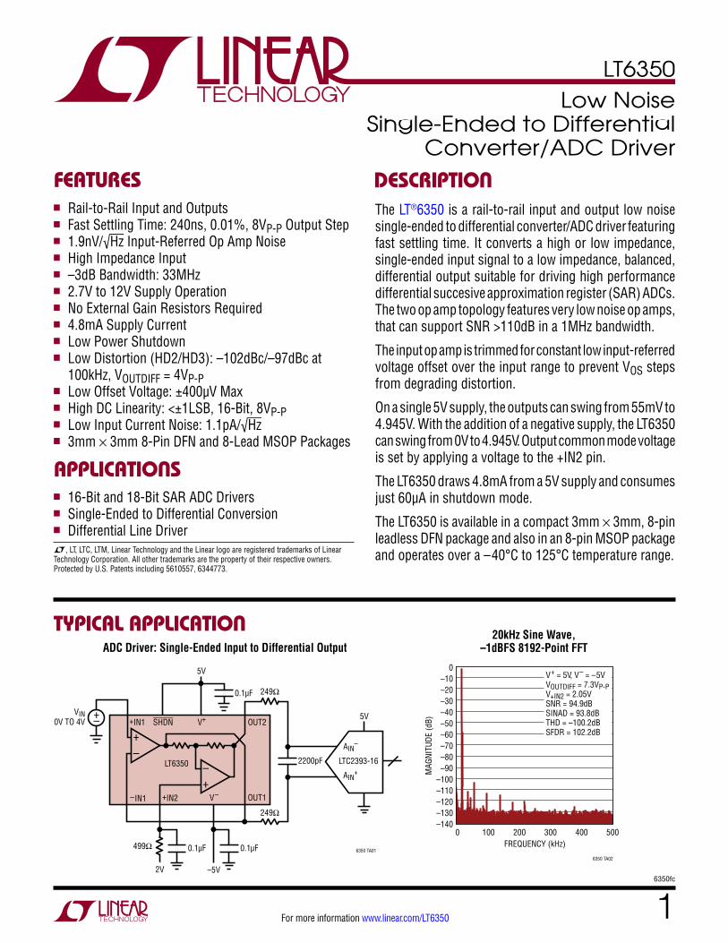
20kHz Sine Wave, –1dBFS 8192-Point FFT
FeaTures
applicaTions
n Rail-to-Rail Input and Outputs n Fast Settling Time: 240ns, 0.01%, 8VP-P Output Stepn 1.9nV/√Hz Input-Referred Op Amp Noisen High Impedance Inputn –3dB Bandwidth: 33MHzn 2.7V to 12V Supply Operationn No External Gain Resistors Requiredn 4.8mA Supply Currentn Low Power Shutdownn Low Distortion (HD2/HD3): –102dBc/–97dBc at
100kHz, VOUTDIFF = 4VP-Pn Low Offset Voltage: ±400µV Maxn High DC Linearity: <±1LSB, 16-Bit, 8VP-Pn Low Input Current Noise: 1.1pA/√Hzn 3mm × 3mm 8-Pin DFN and 8-Lead MSOP Packages
n 16-Bit and 18-Bit SAR ADC Driversn Single-Ended to Differential Conversionn Differential Line Driver
FREQUENCY (kHz)0
–140
MAG
NITU
DE (d
B)
–30
–10–20
–60–50–40
–70–80–90
–110–100
–120–130
0
100 200 500300
6350 TA02
400
V+ = 5V, V– = –5VVOUTDIFF = 7.3VP-PV+IN2 = 2.05VSNR = 94.9dBSINAD = 93.8dBTHD = –100.2dBSFDR = 102.2dB
+– +IN1
–IN1
V+
V–
OUT2
OUT1
SHDN
+IN2
VIN0V TO 4V
5V
5V
0.1µF
0.1µF 0.1µF499Ω
2V –5V
LT6350
6350 TA01
+–
249Ω
249Ω
2200pF
+–
AIN–
AIN+
LTC2393-16
ADC Driver: Single-Ended Input to Differential Output
L, LT, LTC, LTM, Linear Technology and the Linear logo are registered trademarks of Linear Technology Corporation. All other trademarks are the property of their respective owners. Protected by U.S. Patents including 5610557, 6344773.
LT6350
26350fc
For more information www.linear.com/LT6350
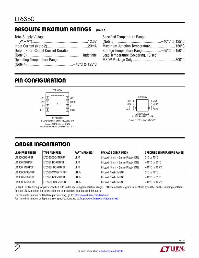
pin conFiguraTion
absoluTe MaxiMuM raTingsTotal Supply Voltage (V+ – V–) ............................................................12.6VInput Current (Note 2) ..........................................±20mAOutput Short-Circuit Current Duration(Note 3) ............................................................ IndefiniteOperating Temperature Range(Note 4) ..................................................–40°C to 125°C
(Note 1)
TOP VIEW
DD PACKAGE8-LEAD (3mm × 3mm) PLASTIC DFN
5
6
7
8
4
3
2
1–IN1
+IN2
V+
OUT1
+IN1
SHDN
V–
OUT2
9
TJMAX = 150°C, θJA = 43°C/W
UNDERSIDE METAL CONNECTED TO V–
1234
–IN1+IN2
V+
OUT1
8765
+IN1SHDNV–
OUT2
TOP VIEW
MS8 PACKAGE8-LEAD PLASTIC MSOP
TJMAX = 150°C, θJA = 250°C/W
orDer inForMaTionLEAD FREE FINISH TAPE AND REEL PART MARKING* PACKAGE DESCRIPTION SPECIFIED TEMPERATURE RANGE
LT6350CDD#PBF LT6350CDD#TRPBF LFJT 8-Lead (3mm × 3mm) Plastic DFN 0°C to 70°C
LT6350IDD#PBF LT6350IDD#TRPBF LFJT 8-Lead (3mm × 3mm) Plastic DFN –40°C to 85°C
LT6350HDD#PBF LT6350HDD#TRPBF LFJT 8-Lead (3mm × 3mm) Plastic DFN –40°C to 125°C
LT6350CMS8#PBF LT6350CMS8#TRPBF LTFJV 8-Lead Plastic MSOP 0°C to 70°C
LT6350IMS8#PBF LT6350IMS8#TRPBF LTFJV 8-Lead Plastic MSOP –40°C to 85°C
LT6350HMS8#PBF LT6350HMS8#TRPBF LTFJV 8-Lead Plastic MSOP –40°C to 125°C
Consult LTC Marketing for parts specified with wider operating temperature ranges. *The temperature grade is identified by a label on the shipping container.Consult LTC Marketing for information on non-standard lead based finish parts.For more information on lead free part marking, go to: http://www.linear.com/leadfree/ For more information on tape and reel specifications, go to: http://www.linear.com/tapeandreel/
Specified Temperature Range(Note 5) ..................................................–40°C to 125°CMaximum Junction Temperature........................... 150°CStorage Temperature Range ...................–65°C to 150°CLead Temperature (Soldering, 10 sec)MSOP Package Only ............................................. 300°C
LT6350
36350fc
For more information www.linear.com/LT6350
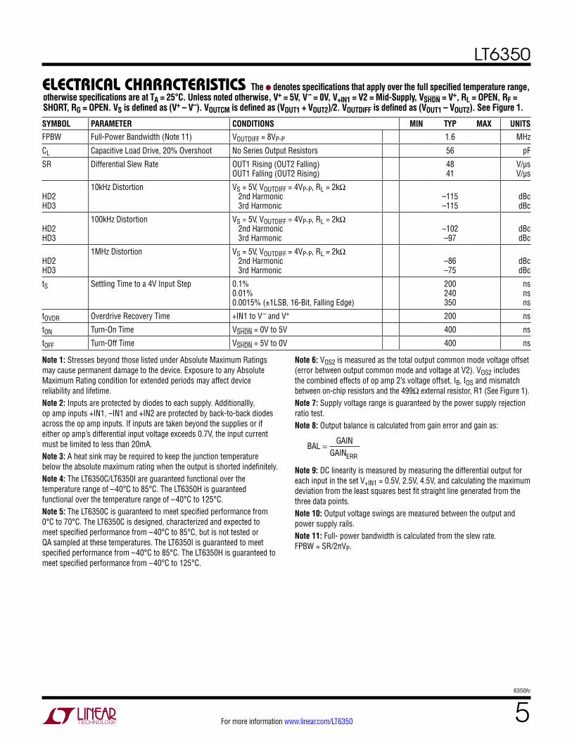
elecTrical characTerisTics
SYMBOL PARAMETER CONDITIONS MIN TYP MAX UNITSVOSDIFF Differential Input-Referred Offset Voltage VS = 5V
V+IN1 = V2 = Mid-Rail V+IN1 = V2 = V–+1.5V to V+ – 0.1V V+IN1 = V2 = V–+1.5V to V+ – 0.1V
l
–0.4 –0.45 –0.77
±0.1
0.4
0.45 1.36
mV mV mV
VS = 3V V+IN1 = V2 = V–+1.5V to V+ – 0.1V V+IN1 = V2 = V–+1.5V to V+ – 0.1V
l
–0.45 –0.8
±0.1
0.45 1.36
mV mV
VS = 10V V+IN1 = V2 = V–+1.5V to V+ – 0.1V V+IN1 = V2 = V–+1.5V to V+ – 0.1V
l
–0.52 –0.78
±0.1
0.52 1.48
mV mV
VOS1 Input Offset Voltage, Op Amp 1 VS = 5V V+IN1 = V–+1.5V to V+ V+IN1 = V– to V+
l
l
–0.35 –1.5
±0.08 ±0.28
0.68 1.5
mV mV
VS = 3V V+IN1 = V–+1.5V to V+ V+IN1 = V– to V+
l
l
–0.35 –1.5
±0.08 ±0.32
0.68 1.5
mV mV
VS = 10V V+IN1 = V–+1.5V to V+ V+IN1 = V– to V+
l
l
–0.68 –1.5
±0.07 ±0.28
0.68 1.5
mV mV
VOS2 Input Offset Voltage, Op Amp 2 (Note 6) VS = 3V, 5V, 10V V+IN1 = V2 = V–+1.5V to V+ – 0.1V
l
–1.0
±0.1
0.66
mV
∆VOSDIFF/∆T Differential Offset Voltage Drift V+IN1 = V2 = V– +1.5V V+IN1 = V2 = V+ –0.1V
l
l
5 5.5
µV/°C µV/°C
IB1 Input Bias Current, Op Amp 1 (at +IN1, –IN1)
V+IN1 = Mid-Supply V+IN1 = V– V+IN1 = V+
l
l
l
–6.8 –8.0
–1.2 –3.0 1.4
2.6
µA µA µA
IOS1 Input Offset Current, Op Amp 1 (at +IN1, –IN1)
V+IN1 = Mid-Supply V+IN1 = V– V+IN1 = V+
l
l
l
–1 –1 –1
±0.1 ±0.1 ±0.1
1 1 1
µA µA µA
I+IN2 Input Bias Current, Op Amp 2 (at +IN2) V+IN1 = V2 = Mid-Supply l 2.5 4.4 µA
IOS2 Input Offest Current, Op Amp 2 V2 = Mid-Supply ±0.1 µA
en1 Input Voltage Noise Density, Op Amp 1 Op Amp Input Referred 1.9 nV/√Hz
in1 Input Current Noise Density, Op Amp 1 1.1 pA/√Hz
en2 Input Voltage Noise Density, Op Amp 2 Op Amp Input Referred 2.1 nV/√Hz
in2 Input Current Noise Density, Op Amp 2 1 pA/√Hz
en(OUT) Differential Output Noise Voltage Density Total Output Noise Including Both Op Amps and On-Chip Resistors. Input Shorted. f = 10kHz
8.2 nV/√Hz
Input Noise Voltage 0.1Hz to 10Hz 300 nVP-P
SNR Output Signal-to-Noise Ratio VOUTDIFF = 8VP-P, 1MHz Noise Bandwidth 110 dB
V+IN1 Input Voltage Range, +IN1 Guaranteed by CMRR1 l V– V+ V
V+IN2 Input Voltage Range, +IN2 Guaranteed by CMRR2 l V– +1.5V V+ –0.1V V
RIN Input Resistance Single-Ended Input at +IN1 4 MΩ
The l denotes specifications that apply over the full specified temperature range, otherwise specifications are at TA = 25°C. Unless noted otherwise, V+ = 5V, V– = 0V, V+IN1 = V2 = Mid-Supply, VSHDN = V+, RL = OPEN, RF = SHORT, RG = OPEN. VS is defined as (V+ – V–). VOUTCM is defined as (VOUT1 + VOUT2)/2. VOUTDIFF is defined as (VOUT1 – VOUT2). See Figure 1.
LT6350
46350fc
For more information www.linear.com/LT6350
elecTrical characTerisTics The l denotes specifications that apply over the full specified temperature range, otherwise specifications are at TA = 25°C. Unless noted otherwise, V+ = 5V, V– = 0V, V+IN1 = V2 = Mid-Supply, VSHDN = V+, RL = OPEN, RF = SHORT, RG = OPEN. VS is defined as (V+ – V–). VOUTCM is defined as (VOUT1 + VOUT2)/2. VOUTDIFF is defined as (VOUT1 – VOUT2). See Figure 1.
SYMBOL PARAMETER CONDITIONS MIN TYP MAX UNITSCIN Input Capacitance Single-Ended Input at +IN1 1.8 pF
CMRR1 Common Mode Rejection Ratio, Op Amp 1 VS = 5V, V+IN1 = V–IN1 = V– +1.5V to V+ VS = 5V, V+IN1 = V–IN1 = V– +1.5V to V+ VS = 5V, V+IN1 = V–IN1 = V– to V+ VS = 3V, V+IN1 = V–IN1 = V– to V+
l
l
l
82 77 72 67
94 94 88 82
dB dB dB dB
CMRR2 Common Mode Rejection Ratio, Op Amp 2 VS = 5V, V+IN1 = V2 = V–+1.5V to V+ –0.1V VS = 3V, V+IN1 = V2 = V–+1.5V to V+ –0.1V VS = 10V, V+IN1 = V2 = V–+1.5V to V+ –0.1V
l
l
l
93 85 96
118 110 118
dB dB dB
PSRR Power Supply Rejection Ratio (∆VS/∆VOSDIFF)
VS = 2.7V to 12V l 80 108 dB
VS Supply Voltage (Note 7) l 2.7 12 V
BAL Output Balance (∆VOUTDIFF/∆VOUTCM) (Note 8)
VOUTDIFF = 2V l 50 68 dB
GAIN Closed-Loop Gain (∆VOUTDIFF/∆(V+IN1 –V2))
∆(V+IN1 –V2) = 4V l 2 V/V
GAINERR Closed-Loop Gain Error l –0.6 ±0.08 0.6 %
∆GAINERR/∆T Closed-Loop Gain Error Drift l 3 ppm/°C
INL DC Linearity (Note 9) V+ = 5V, V– = 0V V+ = 5V, V– = –2V V+ = 5V, V– = –2V, 16-Bit, 8VP-P
230 125 ±1
µV µV
LSB
RINT Internal Resistors 1000 Ω
VOH Output Swing to V+, Either Output (Note 10)
No Load Sourcing 12.5mA
l
l
55 360
170 750
mV mV
VOL Output Swing to V–, Either Output (Note 10)
No Load Sourcing 12.5mA
l
l
55 260
170 460
mV mV
ISC Output Short-Circuit Current V+IN1 = Mid-Rail ±200mV, V–IN1 = Mid-Rail VS = 5V VS = 5V VS = 3V
l
l
±27 ±15 ±15
±45 ±45 ±40
mA mA mA
VIL SHDN Input Logic Low VS = 2.7V to 12V l V– + 0.3 V
VIH SHDN Input Logic High VS = 2.7V to 12V l V– + 2.0 V
ISHDN SHDN Pin Current SHDN = V+
SHDN = V–l
l
–1 –45
–20
1 µA µA
IS Supply Current VS = 3V VS = 5V VS = 5V VS = 10V
l
l
l
4.5
4.8 5.4
8.1 5.8 8.3
10.4
mA mA mA mA
IS(SHDN) Supply Current in Shutdown VS = 3V, VSHDN = VIL VS = 5V, VSHDN = VIL VS = 10V, VSHDN = VIL
l
l
l
43 60 70
220 240 260
µA µA µA
GBW Gain-Bandwidth Product Frequency = 1MHz
Op Amp 1 (Noninverting) Op Amp 2 (Inverting)
85 115
MHz MHz
BW Differential –3dB Small-Signal Bandwidth VOUTDIFF = 100mVP-P VOUTDIFF = 100mVP-P
l
23 19
33
MHz MHz
LT6350
56350fc
For more information www.linear.com/LT6350
Note 1: Stresses beyond those listed under Absolute Maximum Ratings may cause permanent damage to the device. Exposure to any Absolute Maximum Rating condition for extended periods may affect device reliability and lifetime.Note 2: Inputs are protected by diodes to each supply. Additionallly, op amp inputs +IN1, –IN1 and +IN2 are protected by back-to-back diodes across the op amp inputs. If inputs are taken beyond the supplies or if either op amp’s differential input voltage exceeds 0.7V, the input current must be limited to less than 20mA.Note 3: A heat sink may be required to keep the junction temperature below the absolute maximum rating when the output is shorted indefinitely.Note 4: The LT6350C/LT6350I are guaranteed functional over the temperature range of –40°C to 85°C. The LT6350H is guaranteed functional over the temperature range of –40°C to 125°C.Note 5: The LT6350C is guaranteed to meet specified performance from 0°C to 70°C. The LT6350C is designed, characterized and expected to meet specified performance from –40°C to 85°C, but is not tested or QA sampled at these temperatures. The LT6350I is guaranteed to meet specified performance from –40°C to 85°C. The LT6350H is guaranteed to meet specified performance from –40°C to 125°C.
Note 6: VOS2 is measured as the total output common mode voltage offset (error between output common mode and voltage at V2). VOS2 includes the combined effects of op amp 2’s voltage offset, IB, IOS and mismatch between on-chip resistors and the 499Ω external resistor, R1 (See Figure 1).Note 7: Supply voltage range is guaranteed by the power supply rejection ratio test.Note 8: Output balance is calculated from gain error and gain as: BAL
GAINGAINERR
=
Note 9: DC linearity is measured by measuring the differential output for each input in the set V+IN1 = 0.5V, 2.5V, 4.5V, and calculating the maximum deviation from the least squares best fit straight line generated from the three data points.Note 10: Output voltage swings are measured between the output and power supply rails.Note 11: Full- power bandwidth is calculated from the slew rate. FPBW = SR/2�VP.
elecTrical characTerisTics The l denotes specifications that apply over the full specified temperature range, otherwise specifications are at TA = 25°C. Unless noted otherwise, V+ = 5V, V– = 0V, V+IN1 = V2 = Mid-Supply, VSHDN = V+, RL = OPEN, RF = SHORT, RG = OPEN. VS is defined as (V+ – V–). VOUTCM is defined as (VOUT1 + VOUT2)/2. VOUTDIFF is defined as (VOUT1 – VOUT2). See Figure 1.
SYMBOL PARAMETER CONDITIONS MIN TYP MAX UNITSFPBW Full-Power Bandwidth (Note 11) VOUTDIFF = 8VP-P 1.6 MHz
CL Capacitive Load Drive, 20% Overshoot No Series Output Resistors 56 pF
SR Differential Slew Rate OUT1 Rising (OUT2 Falling) OUT1 Falling (OUT2 Rising)
48 41
V/µs V/µs
HD2 HD3
10kHz Distortion VS = 5V, VOUTDIFF = 4VP-P, RL = 2kΩ 2nd Harmonic 3rd Harmonic
–115 –115
dBc dBc
HD2 HD3
100kHz Distortion VS = 5V, VOUTDIFF = 4VP-P, RL = 2kΩ 2nd Harmonic 3rd Harmonic
–102 –97
dBc dBc
HD2 HD3
1MHz Distortion VS = 5V, VOUTDIFF = 4VP-P, RL = 2kΩ 2nd Harmonic 3rd Harmonic
–86 –75
dBc dBc
tS Settling Time to a 4V Input Step 0.1% 0.01% 0.0015% (±1LSB, 16-Bit, Falling Edge)
200 240 350
ns ns ns
tOVDR Overdrive Recovery Time +IN1 to V– and V+ 200 ns
tON Turn-On Time VSHDN = 0V to 5V 400 ns
tOFF Turn-Off Time VSHDN = 5V to 0V 400 ns
LT6350
66350fc
For more information www.linear.com/LT6350
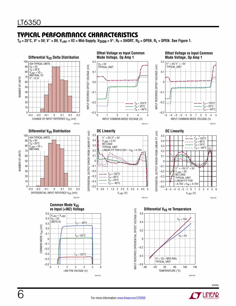
Offset Voltage vs Input Common Mode Voltage, Op Amp 1
Offset Voltage vs Input Common Mode Voltage, Op Amp 1
Common Mode VOS vs Input (+IN2) Voltage Differential VOS vs Temperature
+IN2 PIN VOLTAGE (V)0
–0.5
COM
MON
MOD
E V O
S (m
V)
0.3
0.2
0.1
–0.1
–0.2
–0.3
–0.4
0
0.5
0.4
1 62 3 4 5
6350 G07
V+IN1 = V+IN2VS = 5V(NOTE 6) TA = –40°C
TA = 25°C
TA = 125°C
TEMPERATURE (°C)–60
–0.6
–0.4
–0.2
0
INPU
T RE
FERR
ED D
IFFE
RENT
IAL
OFFS
ET V
OLTA
GE (m
V)
0.4
0.2
0.6
100 140–20 20 60
6350 G09
VS = 10V
V1 = V2 = MID-RAILTYPICAL UNIT
VS = 5V
INPUT COMMON MODE VOLTAGE (V)0
–0.3
INPU
T RE
FERR
ED O
FFSE
T VO
LTAG
E (m
V)
0.1
0.0
–0.1
–0.2
0.2
1 4 52 3
6350 G10
VS = 5VTYPICAL UNIT
TA = –40°CTA = 25°CTA = 125°C
INPUT COMMON MODE VOLTAGE (V)–5
–0.3
INPU
T RE
FERR
ED O
FFSE
T VO
LTAG
E (m
V)
0.1
0
–0.1
–0.2
0.2
–4 4 5–3 –2 –1 0 1
6350 G11
2 3
V+ = 5V, V– = –5VTYPICAL UNIT
TA = –40°CTA = 25°CTA = 125°C
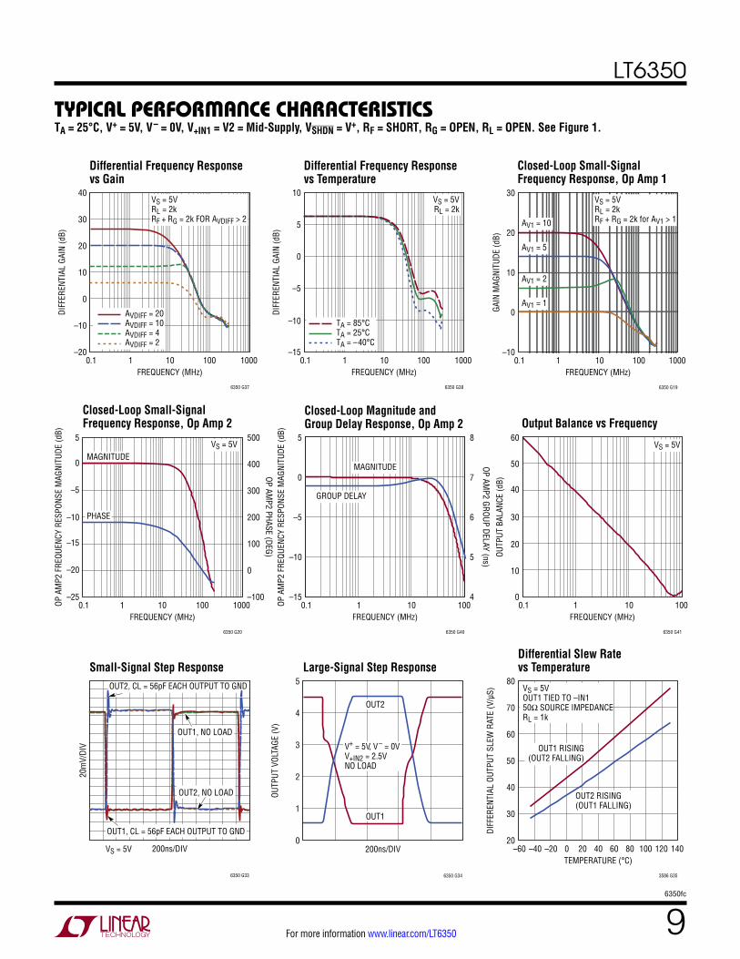
Typical perForMance characTerisTics
Differential VOS Distribution
Differential VOS Delta Distribution
DIFFERENTIAL INPUT REFFERED VOS (mV)–0.3
0
NUM
BER
OF U
NITS
90
80
70
60
50
40
30
20
10
100
0.1 0.2 0.3–0.2 –0.1
6350 G01
0
434 TYPICAL UNITSVS = 5VTA = 25°CV+IN1 = V2 = MID-RAIL
CHANGE OF INPUT REFERRED VOS (mV)–0.3 –0.2
0
NUM
BER
OF U
NITS
90
80
70
60
50
40
30
20
10
100
0.2 0.3–0.1 0 0.1
6350 G02
434 TYPICAL UNITSVS = 5VTA = 25°CV+IN1 = V2 = MID-RAIL TO V+ –0.1V
TA = 25°C, V+ = 5V, V– = 0V, V+IN1 = V2 = Mid-Supply, VSHDN = V+, RF = SHORT, RG = OPEN, RL = OPEN. See Figure 1.
DC Linearity
V+IN1 (V)0
–0.5
–0.4
–0.3
DIFF
EREN
TIAL
OUT
PUT
ERRO
R FR
OM L
INEA
R FI
T (m
V)
0.2
0.3
0.4
0.5
0
0.1
–0.2
–0.1
0.5 1 1.5 2 52.5 3 3.5 4 4.5
6350 G21
TA = –40°CTA = 25°CTA = 85°CTA = 125°C
V– = 0V, V+ = 5VV+IN2 = 2.5VNO LOADTYPICAL UNITLINEAR FIT FOR 0.25V < VIN < 4.75V
DC Linearity
V+IN1 (V)–6
–0.5
DIFF
EREN
TIAL
OUT
PUT
ERRO
R FR
OM L
INEA
R FI
T (m
V)
0.4
0.3
0.2
0.1
0
–0.1
–0.2
–0.3
–0.4
0.5
–5 6–4 –3 –2 –1 0 1 2 3 4 5
6350 G22
TA = –40°CTA = 25°CTA = 85°CTA = 125°C
V– = –5V, V+ = 5VV+IN2 = 0VNO LOADTYPICAL UNITLINEAR FIT FOR –4.75V < VIN < 4.75V
LT6350
76350fc
For more information www.linear.com/LT6350
Input Bias Current vs Input Voltage, Op Amp 2
Input Bias Current vs Temperature, Op Amp 1
Input Bias Current vs Input Voltage, Op Amp 1
V+IN1 (V)0
–4
INPU
T CU
RREN
T +I
N1 (µ
A)
1
0
–1
–3
–2
2
1 52 3
6350 G08
4
VS = 5V
TA = –40°CTA = 25°CTA = 125°C
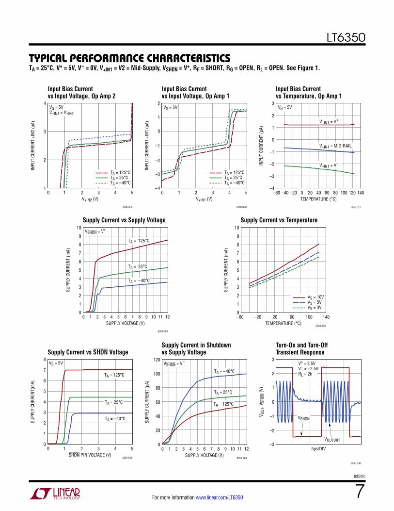
Typical perForMance characTerisTicsTA = 25°C, V+ = 5V, V– = 0V, V+IN1 = V2 = Mid-Supply, VSHDN = V+, RF = SHORT, RG = OPEN, RL = OPEN. See Figure 1.
V+IN2 (V)0
1
INPU
T CU
RREN
T +I
N2 (µ
A)
3
2
4
1 52 3
3586 G35
4
VS = 5VV+IN1 = V+IN2
TA = –40°CTA = 25°CTA = 125°C
TEMPERATURE (°C)–60
–4
INPU
T CU
RREN
T (µ
A)
2
1
0
–1
–2
–3
3
–40 120 140–20 0 20 40 60
6350 G13
80 100
V+IN1 = V–
V+IN1 = MID-RAIL
V+IN1 = V+
VS = 5V
Supply Current vs Supply Voltage
SUPPLY VOLTAGE (V)0
0
SUPP
LY C
URRE
NT (m
A)
9
8
7
6
5
4
3
2
1
10
31 2 11 1254 6 7
6350 G03
1098
VSHDN = V+
TA = 125°C
TA = 25°C
TA = –40°C
Supply Current vs Temperature
TEMPERATURE (°C)–600
SUPP
LY C
URRE
NT (m
A)
9
8
7
6
5
4
3
2
1
10
60 100 140–20 20
6350 G04
VS = 3VVS = 5VVS = 10V
Supply Current vs SHDN Voltage
SHDN PIN VOLTAGE (V)0
0
SUPP
LY C
URRE
NT(m
A)
7
6
5
4
3
2
1
8
1 4 52
6350 G05
3
TA = –40°C
TA = 25°C
TA = 125°C
VS = 5V
Supply Current in Shutdown vs Supply Voltage
SUPPLY VOLTAGE (V)0
0
SUPP
LY C
URRE
NT (µ
A)
100
80
60
40
20
120
1 11 123 42 5 6 7 8
6350 G06
9 10
VSHDN = V–
TA = –40°C
TA = 25°C
TA = 125°C
Turn-On and Turn-Off Transient Response
5µs/DIV–3
V OUT
, VSH
DN (V
)
2
1
0
–1
–2
3
6350 G43
V+ = 2.5VV– = –2.5VRL = 2k
VSHDN
VOUTDIFF
LT6350
86350fc
For more information www.linear.com/LT6350
Output Settling Time vs Output Step
Output Settling Time vs Output Step
Typical perForMance characTerisTicsTA = 25°C, V+ = 5V, V– = 0V, V+IN1 = V2 = Mid-Supply, VSHDN = V+, RF = SHORT, RG = OPEN, RL = OPEN. See Figure 1.
DIFFERENTIAL OUTPUT STEP (V)–8
0
SETT
LING
TIM
E (n
s)
250
200
150
100
50
300
8–6 –4 –2
6350 G35
0 2 4 6
2mV
20mV 20mV
2mV
VS = 5V
DIFFERENTIAL OUTPUT STEP (V)–20
0
50
SETT
LING
TIM
E (n
s)
300
350
200
250
100
150
400
20–15 –10 –5
6350 G36
0 5 10 15
0.01%
2mV
20mV
VS = 10V
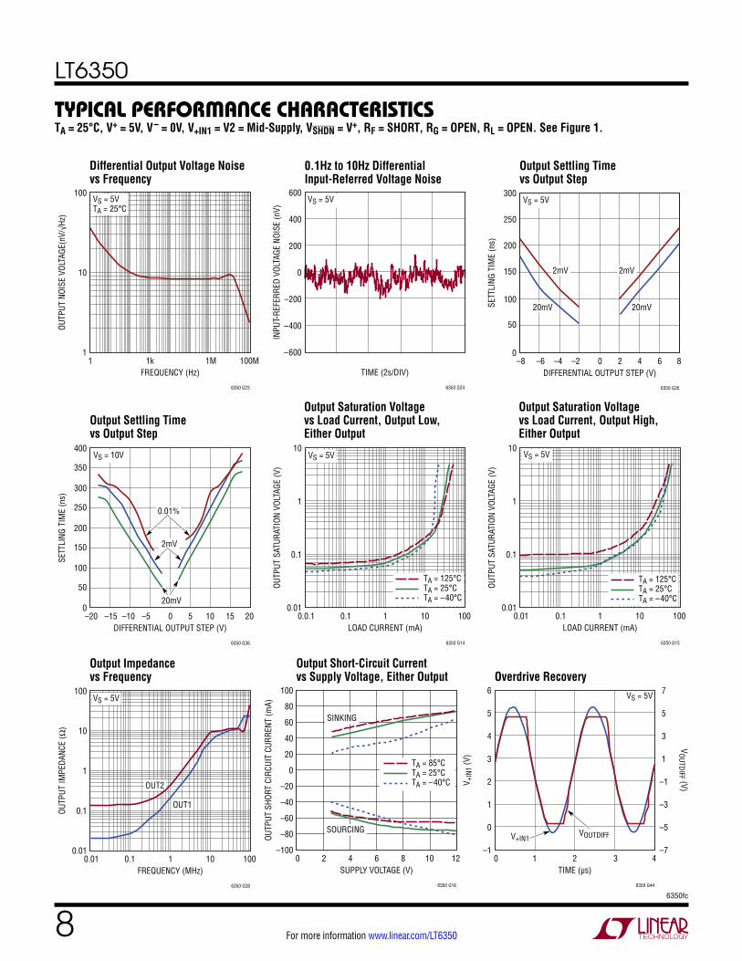
Differential Output Voltage Noise vs Frequency
FREQUENCY (Hz)1
1
OUTP
UT N
OISE
VOL
TAGE
(nV/
√Hz)
10
100
1M 100M1k
6350 G23
VS = 5VTA = 25°C
0.1Hz to 10Hz Differential Input-Referred Voltage Noise
TIME (2s/DIV)
–600
INPU
T-RE
FERR
ED V
OLTA
GE N
OISE
(nV)
200
400
0
–200
–400
600
6350 G24
VS = 5V
Output Impedance vs Frequency
FREQUENCY (MHz)0.01
0.01
OUTP
UT IM
PEDA
NCE
(Ω) 10
1
0.1
100
1000.1
6350 G28
1 10
VS = 5V
OUT2
OUT1
Overdrive Recovery
VOUTDIFF
TIME (µs)0
–1
V +IN
1 (V
)
5
4
3
2
1
0
6
–7
VOUTDIFF (V)
5
3
1
–1
–3
–5
7
41 2
6350 G44
3
V+IN1
VS = 5V
Output Saturation Voltage vs Load Current, Output Low, Either Output
LOAD CURRENT (mA)0.0.1
0.01
OUTP
UT S
ATUR
ATIO
N VO
LTAG
E (V
)
1
0.1
10
0.1 1001
6350 G14
10
TA = –40°CTA = 25°CTA = 125°C
VS = 5V
Output Saturation Voltage vs Load Current, Output High, Either Output
LOAD CURRENT (mA)0.01
0.01
OUTP
UT S
ATUR
ATIO
N VO
LTAG
E (V
)1
0.1
10
1000.1 1
6350 G15
10
VS = 5V
TA = –40°CTA = 25°CTA = 125°C
Output Short-Circuit Current vs Supply Voltage, Either Output
SUPPLY VOLTAGE (V)0
–100
OUTP
UT S
HORT
CIR
CUIT
CUR
RENT
(mA) 80
60
40
20
0
–20
–40
–60
–80
100
2 10 124 6 8
6350 G16
SINKING
SOURCING
TA = –40°CTA = 25°CTA = 85°C
LT6350
96350fc
For more information www.linear.com/LT6350
Small-Signal Step Response
200ns/DIV
20m
V/DI
V
6350 G33
VS = 5V
OUT1, CL = 56pF EACH OUTPUT TO GND
OUT2, NO LOAD
OUT1, NO LOAD
OUT2, CL = 56pF EACH OUTPUT TO GND
Differential Frequency Response vs Gain
Differential Frequency Response vs Temperature
Closed-Loop Magnitude and Group Delay Response, Op Amp 2 Output Balance vs Frequency
Large-Signal Step Response
FREQUENCY (MHz)0.1
–15
OP A
MP2
FRE
QUEN
CY R
ESPO
NSE
MAG
NITU
DE (d
B)
OP AMP2 GROUP DELAY (ns)
0
–5
–10
5
4
7
6
5
8
1 10010
6350 G40
GROUP DELAY
MAGNITUDE
Typical perForMance characTerisTicsTA = 25°C, V+ = 5V, V– = 0V, V+IN1 = V2 = Mid-Supply, VSHDN = V+, RF = SHORT, RG = OPEN, RL = OPEN. See Figure 1.
FREQUENCY (MHz)0.1
0
OUTP
UT B
ALAN
CE (d
B)
50
40
30
20
10
60
1001
6350 G41
10
VS = 5V
OUT2
OUT1
200ns/DIV0
OUTP
UT V
OLTA
GE (V
)
4
3
2
1
5
6350 G34
V+ = 5V, V– = 0VV+IN2 = 2.5VNO LOAD
FREQUENCY (MHz)0.1
–20
DIFF
EREN
TIAL
GAI
N (d
B)
30
20
10
0
–10
40
1 100010
6350 G37
100
AVDIFF = 2AVDIFF = 4AVDIFF = 10AVDIFF = 20
VS = 5VRL = 2kRF + RG = 2k FOR AVDIFF > 2
FREQUENCY (MHz)0.1
–15
DIFF
EREN
TIAL
GAI
N (d
B)
5
0
–5
–10
10
10001 10
6350 G38
100
TA = –40°CTA = 25°CTA = 85°C
VS = 5VRL = 2k
Differential Slew Rate vs Temperature
TEMPERATURE (°C)–60
20
DIFF
EREN
TIAL
OUT
PUT
SLEW
RAT
E (V
/µS)
70
60
50
40
30
80
–40 100 120 140–20 0 20
3586 G35
40 60 80
OUT1 RISING(OUT2 FALLING)
VS = 5VOUT1 TIED TO –IN150Ω SOURCE IMPEDANCERL = 1k
OUT2 RISING(OUT1 FALLING)
Closed-Loop Small-Signal Frequency Response, Op Amp 1
Closed-Loop Small-Signal Frequency Response, Op Amp 2
FREQUENCY (MHz)0.1
–25
OP A
MP2
FRE
QUEN
CY R
ESPO
NSE
MAG
NITU
DE (d
B)
OP AMP2 PHASE (DEG)
–5
0
–10
–15
–20
5
–100
400
200
300
100
0
500
1 100010 100
6350 G20
VS = 5VMAGNITUDE
PHASE
FREQUENCY (MHz)0.1
–10
GAIN
MAG
NITU
DE (d
B) 20
10
0
30
1 100010 100
6350 G19
VS = 5VRL = 2kRF + RG = 2k for AV1 > 1AV1 = 10
AV1 = 5
AV1 = 2
AV1 = 1
LT6350
106350fc
For more information www.linear.com/LT6350
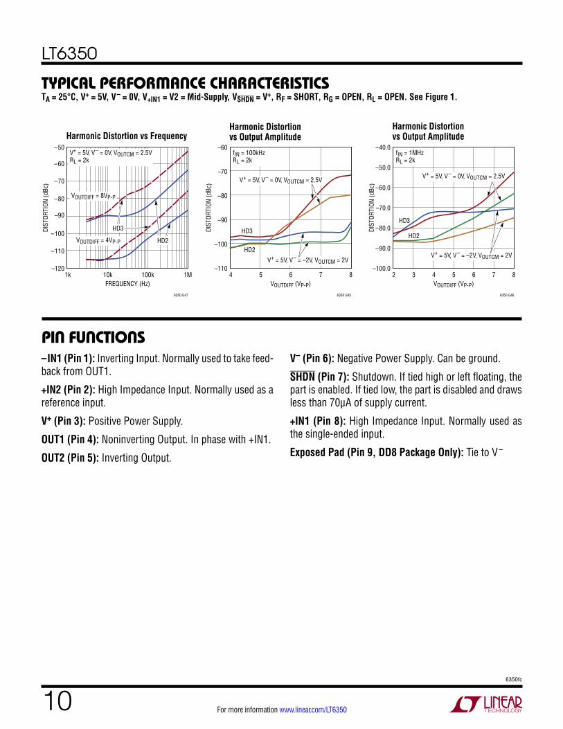
pin FuncTions–IN1 (Pin 1): Inverting Input. Normally used to take feed-back from OUT1.
+IN2 (Pin 2): High Impedance Input. Normally used as a reference input.
V+ (Pin 3): Positive Power Supply.
OUT1 (Pin 4): Noninverting Output. In phase with +IN1.
OUT2 (Pin 5): Inverting Output.
V– (Pin 6): Negative Power Supply. Can be ground.
SHDN (Pin 7): Shutdown. If tied high or left floating, the part is enabled. If tied low, the part is disabled and draws less than 70μA of supply current.
+IN1 (Pin 8): High Impedance Input. Normally used as the single-ended input.
Exposed Pad (Pin 9, DD8 Package Only): Tie to V–
FREQUENCY (Hz)1k
–120
DIST
ORTI
ON (d
Bc)
–80
–90
–100
–110
–50
–70
–60
1M10k
6350 G47
100k
V+ = 5V, V– = 0V, VOUTCM = 2.5VRL = 2k
VOUTDIFF = 4VP-P
VOUTDIFF = 8VP-P
HD3
HD2HD3
VOUTDIFF (VP-P)4
–110
DIST
ORTI
ON (d
Bc)
–70
–80
–90
–100
–60
85
6350 G45
6 7
HD2
fIN = 100kHzRL = 2k
V+ = 5V, V– = 0V, VOUTCM = 2.5V
V+ = 5V, V– = –2V, VOUTCM = 2V
VOUTDIFF (VP-P)2
–100.0
DIST
ORTI
ON (d
Bc)
–60.0
–70.0
–80.0
–90.0
–40.0
–50.0
83 4
6350 G46
5 6 7
V+ = 5V, V– = –2V, VOUTCM = 2V
HD2
HD3
fIN = 1MHzRL = 2k
V+ = 5V, V– = 0V, VOUTCM = 2.5V
Harmonic Distortion vs FrequencyHarmonic Distortion vs Output Amplitude
Harmonic Distortion vs Output Amplitude
Typical perForMance characTerisTicsTA = 25°C, V+ = 5V, V– = 0V, V+IN1 = V2 = Mid-Supply, VSHDN = V+, RF = SHORT, RG = OPEN, RL = OPEN. See Figure 1.
LT6350
116350fc
For more information www.linear.com/LT6350
block DiagraM
8 6 5
+IN1
1–IN1
V–
1k1k
3
V+
OUT2
4
OUT1
SHDN
2+IN2
6350 BD
BIAS
7
–
+
+
_
OP AMP 1
OP AMP 2
Dc TesT circuiT
+–+–
+IN1
–IN1
RF
RG
V+
V–
OUT2
OUT1
SHDN
V+IN1
VSHDN
+IN2
V1
V+
0.1µF
0.1µF 0.1µFR1
499Ω
V2 V–
LT6350
6350 TC
+–
+–
+–
VOUT1
VOUT2
–
+
VOUTDIFF
RL
Figure 1. DC Test Circuit.
LT6350
126350fc
For more information www.linear.com/LT6350
operaTionThe LT6350 is a low noise single-ended to differential converter /ADC driver. It converts a high or low impedance, single-ended input signal to a low impedance, balanced differential output suitable for driving high performance differential sucessive approximation register (SAR) ADCs. The closed loop –3dB bandwidth for the typical gain-of-two configuration is 33MHz.
The LT6350 uses a two op amp topology as shown in the Block Diagram: at the input is one fully uncommitted op amp with both inputs and output brought out to pins. This is followed by an op amp internally hardwired and optimally compensated as a unity-gain inverter with its input connected to the output of the first op amp. The noninverting input of the inverting op amp is brought out to a pin and is used to set the output common mode voltage level. The outputs of the two op amps are therefore 180° out-of-phase and provide a low impedance differential drive for differential-input analog to digital converters. The outputs of the LT6350 can swing rail-to-rail and can source or sink a transient 45mA of current. The outputs are designed to drive 40pF to ground or 20pF differentially. Load capacitances larger than 40pF should be decoupled from each output with at least 25Ω of series resistance.
The LT6350 features very low noise op amps to support signal-to-noise ratios >110dB.
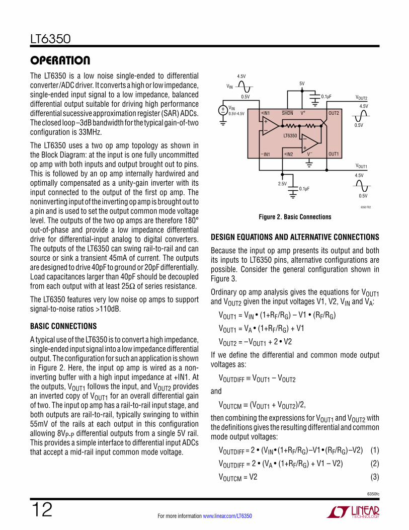
BASIC CONNECTIONS
A typical use of the LT6350 is to convert a high impedance, single-ended input signal into a low impedance differential output. The configuration for such an application is shown in Figure 2. Here, the input op amp is wired as a non-inverting buffer with a high input impedance at +IN1. At the outputs, VOUT1 follows the input, and VOUT2 provides an inverted copy of VOUT1 for an overall differential gain of two. The input op amp has a rail-to-rail input stage, and both outputs are rail-to-rail, typically swinging to within 55mV of the rails at each output in this configuration allowing 8VP-P differential outputs from a single 5V rail. This provides a simple interface to differential input ADCs that accept a mid-rail input common mode voltage.
+–+–
+IN1
–IN1
V+
V–
OUT2
OUT1
SHDN
+IN2
0.5V
5V4.5V
0.1µF
0.1µF2.5V
LT6350
6350 F02
+–
VOUT1
VIN
VIN0.5V-4.5V
VOUT2
0.5V
4.5V
0.5V
4.5V
Figure 2. Basic Connections
DESIGN EQUATIONS AND ALTERNATIVE CONNECTIONS
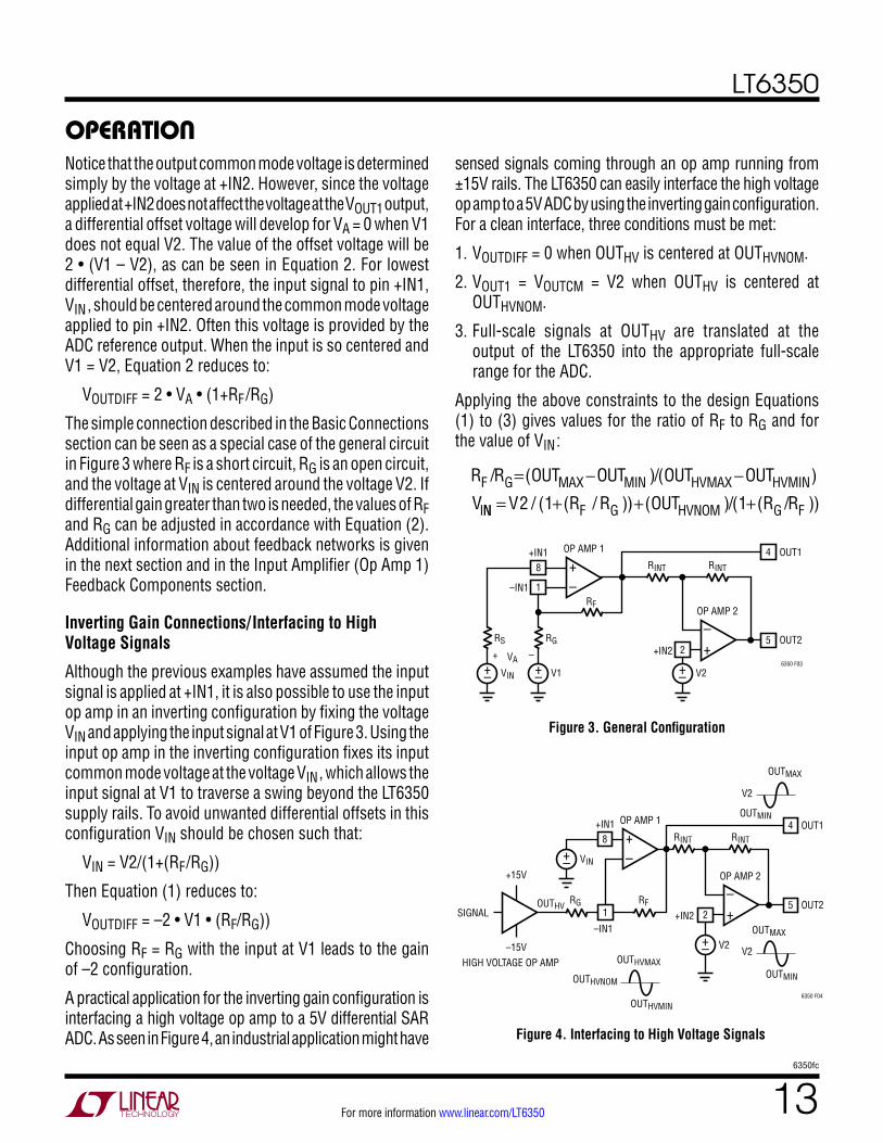
Because the input op amp presents its output and both its inputs to LT6350 pins, alternative configurations are possible. Consider the general configuration shown in Figure 3.
Ordinary op amp analysis gives the equations for VOUT1 and VOUT2 given the input voltages V1, V2, VIN and VA:
VOUT1 = VIN • (1+RF/RG) – V1 • (RF/RG)
VOUT1 = VA • (1+RF/RG) + V1
VOUT2 = –VOUT1 + 2 • V2
If we define the differential and common mode output voltages as:
VOUTDIFF ≡ VOUT1 – VOUT2
and
VOUTCM ≡ (VOUT1 + VOUT2)/2,
then combining the expressions for VOUT1 and VOUT2 with the definitions gives the resulting differential and common mode output voltages:
VOUTDIFF = 2 • (VIN• (1+RF/RG)–V1• (RF/RG)–V2) (1)
VOUTDIFF = 2 • (VA • (1+RF/RG) + V1 – V2) (2)
VOUTCM = V2 (3)
LT6350
136350fc
For more information www.linear.com/LT6350
+–
–+
+–
+–
+–
RS RG
RF
RINT RINT
OUT1
OUT2
VIN V1 V2
VA+ –
–IN1
+IN1
+IN2
OP AMP 1
OP AMP 2
6350 F03
8
1
2
4
5
Figure 3. General Configuration
Notice that the output common mode voltage is determined simply by the voltage at +IN2. However, since the voltage applied at +IN2 does not affect the voltage at the VOUT1 output, a differential offset voltage will develop for VA = 0 when V1 does not equal V2. The value of the offset voltage will be 2 • (V1 – V2), as can be seen in Equation 2. For lowest differential offset, therefore, the input signal to pin +IN1, VIN, should be centered around the common mode voltage applied to pin +IN2. Often this voltage is provided by the ADC reference output. When the input is so centered and V1 = V2, Equation 2 reduces to:
VOUTDIFF = 2 • VA • (1+RF /RG)
The simple connection described in the Basic Connections section can be seen as a special case of the general circuit in Figure 3 where RF is a short circuit, RG is an open circuit, and the voltage at VIN is centered around the voltage V2. If differential gain greater than two is needed, the values of RF and RG can be adjusted in accordance with Equation (2). Additional information about feedback networks is given in the next section and in the Input Amplifier (Op Amp 1) Feedback Components section.
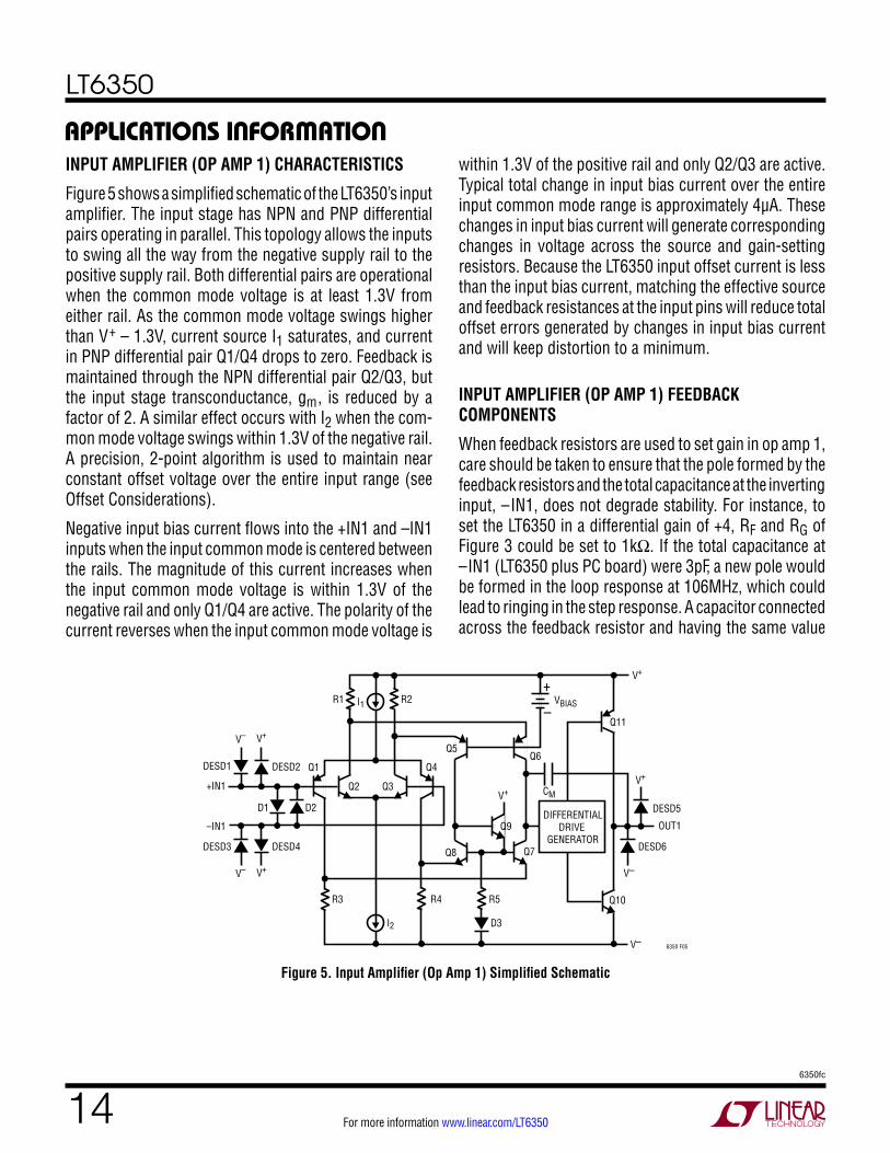
Inverting Gain Connections/ Interfacing to High Voltage Signals
Although the previous examples have assumed the input signal is applied at +IN1, it is also possible to use the input op amp in an inverting configuration by fixing the voltage VIN and applying the input signal at V1 of Figure 3. Using the input op amp in the inverting configuration fixes its input common mode voltage at the voltage VIN, which allows the input signal at V1 to traverse a swing beyond the LT6350 supply rails. To avoid unwanted differential offsets in this configuration VIN should be chosen such that:
VIN = V2/(1+(RF/RG))
Then Equation (1) reduces to:
VOUTDIFF = –2 • V1 • (RF/RG))
Choosing RF = RG with the input at V1 leads to the gain of –2 configuration.
A practical application for the inverting gain configuration is interfacing a high voltage op amp to a 5V differential SAR ADC. As seen in Figure 4, an industrial application might have
operaTion
–+
+–
+–+–
RFRG
RINT RINT
OUT1
OUTMAX
OUTMIN
OUT2
VIN
V2
V2
OUTMAX
OUTMIN
OUTHV
V2OUTHVMAX
OUTHVNOM
OUTHVMIN
–IN1
+IN1
+IN2
–15V
+15V
OP AMP 1
OP AMP 2
6350 F04
SIGNAL
HIGH VOLTAGE OP AMP
8
1 25
4
Figure 4. Interfacing to High Voltage Signals
sensed signals coming through an op amp running from ±15V rails. The LT6350 can easily interface the high voltage op amp to a 5V ADC by using the inverting gain configuration. For a clean interface, three conditions must be met:
1. VOUTDIFF = 0 when OUTHV is centered at OUTHVNOM.
2. VOUT1 = VOUTCM = V2 when OUTHV is centered at OUTHVNOM.
3. Full-scale signals at OUTHV are translated at the output of the LT6350 into the appropriate full-scale range for the ADC.
Applying the above constraints to the design Equations (1) to (3) gives values for the ratio of RF to RG and for the value of VIN:
R R OUT OUT OUT OUT
VF G MAX MIN HVMAX HVMIN
I
/ ( )/( )= − −
NN F G HVNOM G FV R R OUT R R= + + +2 1 1/ ( ( / )) ( )/( ( / ))
LT6350
146350fc
For more information www.linear.com/LT6350
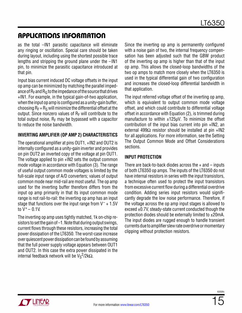
INPUT AMPLIFIER (OP AMP 1) CHARACTERISTICS
Figure 5 shows a simplified schematic of the LT6350’s input amplifier. The input stage has NPN and PNP differential pairs operating in parallel. This topology allows the inputs to swing all the way from the negative supply rail to the positive supply rail. Both differential pairs are operational when the common mode voltage is at least 1.3V from either rail. As the common mode voltage swings higher than V+ – 1.3V, current source I1 saturates, and current in PNP differential pair Q1/Q4 drops to zero. Feedback is maintained through the NPN differential pair Q2/Q3, but the input stage transconductance, gm, is reduced by a factor of 2. A similar effect occurs with I2 when the com-mon mode voltage swings within 1.3V of the negative rail. A precision, 2-point algorithm is used to maintain near constant offset voltage over the entire input range (see Offset Considerations).
Negative input bias current flows into the +IN1 and –IN1 inputs when the input common mode is centered between the rails. The magnitude of this current increases when the input common mode voltage is within 1.3V of the negative rail and only Q1/Q4 are active. The polarity of the current reverses when the input common mode voltage is
applicaTions inForMaTionwithin 1.3V of the positive rail and only Q2/Q3 are active. Typical total change in input bias current over the entire input common mode range is approximately 4µA. These changes in input bias current will generate corresponding changes in voltage across the source and gain-setting resistors. Because the LT6350 input offset current is less than the input bias current, matching the effective source and feedback resistances at the input pins will reduce total offset errors generated by changes in input bias current and will keep distortion to a minimum.
INPUT AMPLIFIER (OP AMP 1) FEEDBACK COMPONENTS
When feedback resistors are used to set gain in op amp 1, care should be taken to ensure that the pole formed by the feedback resistors and the total capacitance at the inverting input, –IN1, does not degrade stability. For instance, to set the LT6350 in a differential gain of +4, RF and RG of Figure 3 could be set to 1kΩ. If the total capacitance at –IN1 (LT6350 plus PC board) were 3pF, a new pole would be formed in the loop response at 106MHz, which could lead to ringing in the step response. A capacitor connected across the feedback resistor and having the same value
DIFFERENTIALDRIVE
GENERATOR
+
–R1 R2
R3 R4 R5
Q2 Q3
Q5Q6
Q9
Q8 Q7
Q10
Q11
Q1 Q4
I1
I2 D3
D2D1
DESD2
DESD4DESD3
DESD1
+IN1
–IN1
DESD5
DESD6
VBIAS
CM
V+
V+V+
V–
V+V–
V+
V–
V–
6350 F05
OUT1
Figure 5. Input Amplifier (Op Amp 1) Simplified Schematic
LT6350
156350fc
For more information www.linear.com/LT6350
applicaTions inForMaTionas the total –IN1 parasitic capacitance will eliminate any ringing or oscillation. Special care should be taken during layout, including using the shortest possible trace lengths and stripping the ground plane under the –IN1 pin, to minimize the parasitic capacitance introduced at that pin.
Input bias current induced DC voltage offsets in the input op amp can be minimized by matching the parallel imped-ance of RF and RG to the impedance of the source that drives +IN1. For example, in the typical gain-of-two application, when the input op amp is configured as a unity-gain buffer, choosing RF = RS will minimize the differential offset at the output. Since nonzero values of RF will contribute to the total output noise, RF may be bypassed with a capacitor to reduce the noise bandwidth.
INVERTING AMPLIFIER (OP AMP 2) CHARACTERISTICS
The operational amplifier at pins OUT1, +IN2 and OUT2 is internally configured as a unity-gain inverter and provides on pin OUT2 an inverted copy of the voltage at pin OUT1. The voltage applied to pin +IN2 sets the output common mode voltage in accordance with Equation (3). The range of useful output common mode voltages is limited by the full-scale input range of A/D converters; values of output common mode near mid-rail are most useful. The op amp used for the inverting buffer therefore differs from the input op amp primarily in that its input common mode range is not rail-to-rail: the inverting op amp has an input stage that functions over the input range from V– + 1.5V to V+ – 0.1V.
The inverting op amp uses tightly matched, 1k on-chip re-sistors to set the gain of –1. Note that during output swings, current flows through these resistors, increasing the total power dissipation of the LT6350. The worst-case increase over quiescent power dissipation can be found by assuming that the full power supply voltage appears between OUT1 and OUT2. In this case the extra power dissipated in the internal feedback network will be VS
2/2kΩ.
Since the inverting op amp is permanently configured with a noise gain of two, the internal frequency compen-sation has been adjusted such that the GBW product of the inverting op amp is higher than that of the input op amp. This allows the closed-loop bandwidths of the two op amps to match more closely when the LT6350 is used in the typical differential gain of two configuration and increases the closed-loop differential bandwidth in that application.
The input referred voltage offset of the inverting op amp, which is equivalent to output common mode voltage offset, and which could contribute to differential voltage offset in accordance with Equation (2), is trimmed during manufacture to within ±125µV. To minimize the offset contribution of the input bias current into pin +IN2, an external 499Ω resistor should be installed at pin +IN2 for all applications. For more information, see the Setting The Output Common Mode and Offset Considerations sections.
INPUT PROTECTION
There are back-to-back diodes across the + and – inputs of both LT6350 op amps. The inputs of the LT6350 do not have internal resistors in series with the input transistors, a technique often used to protect the input transistors from excessive current flow during a differential overdrive condition. Adding series input resistors would signifi-cantly degrade the low noise performance. Therefore, if the voltage across the op amp input stages is allowed to exceed ±0.7V, steady-state current conducted though the protection diodes should be externally limited to ±20mA. The input diodes are rugged enough to handle transient currents due to amplifier slew rate overdrive or momentary clipping without protection resistors.
LT6350
166350fc
For more information www.linear.com/LT6350
applicaTions inForMaTionDriving the input signal sufficiently beyond the power supply rails will cause the input transistors to saturate. When saturation occurs, the amplifier loses a stage of phase inversion and the output tries to invert. Diodes D1 and D2 (Figure 5) forward bias and hold the output within a diode drop of the input signal. With very heavy input overdrive the output of op amp 1 could invert . To avoid this inversion, limit the input overdrive to 0.5V beyond the power supply rails.
OUTPUT VOLTAGE RANGE
The outputs of the LT6350 typically swing to within 55mV of the upper and lower supply rails when driving a purely capacitive load such as at the switched-capacitor input stage of a SAR ADC. The LT6350 can therefore share a single 5V supply with the SAR ADC and drive a full 8VP-P differential around an input common mode voltage between 2.055V and 2.945V. A modest negative supply can be added to allow the LT6350 to swing all the way to 0V in systems where the ADC requires a true 0V-referenced signal or when the input common mode range of the ADC is restricted to be lower than 2.055V. Some SAR ADCs use 2V as the input common mode voltage with a full-scale input signal range at each input of 0V to 4V. The outputs of the LT6350 can swing 7.78VP-P differentially around a 2V common mode voltage, which is a loss of only 0.24dB of the full-scale range of such ADCs.
+–
+IN1
–IN1
V+
V–
OUT2
OUT1
SHDN
+IN2
VIN
5V
5V
0.1µF
0.1µF2V
LT6350
6350 F06
+–
CCM
RS
RFILT
RFILT
RS
CDIFF
CCM
+–
AIN+
AIN–ADC
Figure 6. Driving an ADC
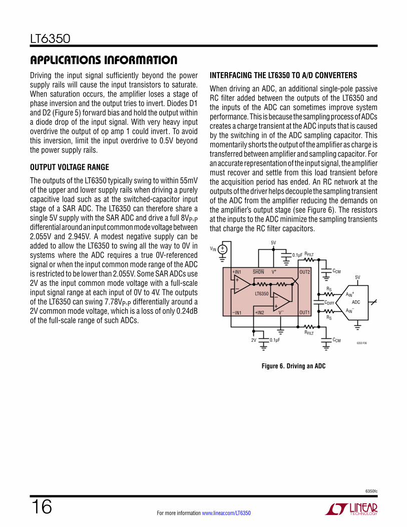
INTERFACING THE LT6350 TO A/D CONVERTERS
When driving an ADC, an additional single-pole passive RC filter added between the outputs of the LT6350 and the inputs of the ADC can sometimes improve system performance. This is because the sampling process of ADCs creates a charge transient at the ADC inputs that is caused by the switching in of the ADC sampling capacitor. This momentarily shorts the output of the amplifier as charge is transferred between amplifier and sampling capacitor. For an accurate representation of the input signal, the amplifier must recover and settle from this load transient before the acquisition period has ended. An RC network at the outputs of the driver helps decouple the sampling transient of the ADC from the amplifier reducing the demands on the amplifier’s output stage (see Figure 6). The resistors at the inputs to the ADC minimize the sampling transients that charge the RC filter capacitors.
LT6350
176350fc
For more information www.linear.com/LT6350
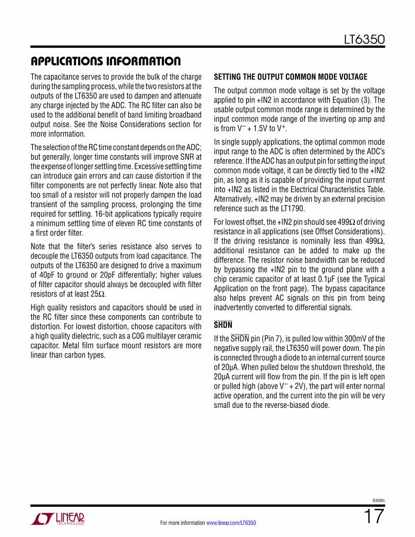
applicaTions inForMaTionThe capacitance serves to provide the bulk of the charge during the sampling process, while the two resistors at the outputs of the LT6350 are used to dampen and attenuate any charge injected by the ADC. The RC filter can also be used to the additional benefit of band limiting broadband output noise. See the Noise Considerations section for more information.
The selection of the RC time constant depends on the ADC; but generally, longer time constants will improve SNR at the expense of longer settling time. Excessive settling time can introduce gain errors and can cause distortion if the filter components are not perfectly linear. Note also that too small of a resistor will not properly dampen the load transient of the sampling process, prolonging the time required for settling. 16-bit applications typically require a minimum settling time of eleven RC time constants of a first order filter.
Note that the filter’s series resistance also serves to decouple the LT6350 outputs from load capacitance. The outputs of the LT6350 are designed to drive a maximum of 40pF to ground or 20pF differentially; higher values of filter capacitor should always be decoupled with filter resistors of at least 25Ω.
High quality resistors and capacitors should be used in the RC filter since these components can contribute to distortion. For lowest distortion, choose capacitors with a high quality dielectric, such as a C0G multilayer ceramic capacitor. Metal film surface mount resistors are more linear than carbon types.
SETTING THE OUTPUT COMMON MODE VOLTAGE
The output common mode voltage is set by the voltage applied to pin +IN2 in accordance with Equation (3). The usable output common mode range is determined by the input common mode range of the inverting op amp and is from V– + 1.5V to V+.
In single supply applications, the optimal common mode input range to the ADC is often determined by the ADC’s reference. If the ADC has an output pin for setting the input common mode voltage, it can be directly tied to the +IN2 pin, as long as it is capable of providing the input current into +IN2 as listed in the Electrical Characteristics Table. Alternatively, +IN2 may be driven by an external precision reference such as the LT1790.
For lowest offset, the +IN2 pin should see 499Ω of driving resistance in all applications (see Offset Considerations). If the driving resistance is nominally less than 499Ω, additional resistance can be added to make up the difference. The resistor noise bandwidth can be reduced by bypassing the +IN2 pin to the ground plane with a chip ceramic capacitor of at least 0.1µF (see the Typical Application on the front page). The bypass capacitance also helps prevent AC signals on this pin from being inadvertently converted to differential signals.
SHDN
If the SHDN pin (Pin 7), is pulled low within 300mV of the negative supply rail, the LT6350 will power down. The pin is connected through a diode to an internal current source of 20µA. When pulled below the shutdown threshold, the 20µA current will flow from the pin. If the pin is left open or pulled high (above V– + 2V), the part will enter normal active operation, and the current into the pin will be very small due to the reverse-biased diode.
LT6350
186350fc
For more information www.linear.com/LT6350
–+
+–
+–
+–RS
RG
R+IN2
RF
RINT RINT
VOSOUT1
VOSOUT2
VOS1
VOS2
–IN1
+IN1
+IN2
OP AMP 1
OP AMP 2
6350 F07
IB1 +IOS1
2
IB1 –IOS1
2
IB2 –IOS2
2
IB2 +IOS2
2
Figure 7. Offset Model
applicaTions inForMaTionIn shutdown, all biasing current sources are shut off, and the output pins, OUT1 and OUT2, each appear as open collectors with non-linear capacitors in parallel and steering diodes to either supply. Because of the non-linear capacitance, the outputs still have the ability to sink and source small amounts of transient current if driven with significant voltage transients. The input protection diodes between +IN1 and +IN2 can still conduct if voltage tran-sients at the input exceed 700mV. All other inputs also have ESD protection diodes that can conduct when the applied voltage exceeds 700mV. Using the SHDN feature to wire-OR outputs together is not recommended.
The turn-on and turn off times between the shutdown and active states are typically 400ns.
ESD
The LT6350 has ESD protection diodes on all inputs and outputs. The diodes are reverse biased during normal operation. If input pins are driven beyond either supply, large currents will flow through these diodes. If the current is transient and limited to 100mA or less, no damage to the device will occur.
OFFSET CONSIDERATIONS
For excellent offset and distortion performance, both the common mode and differential mode output voltage off-sets are trimmed during manufacturing.
Figure 7 shows the contributors to DC offset voltage in the LT6350.
The resulting DC offset voltages at pin OUT1 and OUT2 can be calculated:
VOSOUT1 = VOS1•(1+RF/RG) + IB1•(RF-RS•(1+RF/RG)) – (IOS1/2)•(RF+RS•(1+RF/RG))
VOSOUT2 = –VOSOUT1 + 2•VOS2 + IB2•(RINT–2•R+IN2) – (IOS2/2)•(RINT + 2•R+IN2)
Using the above equations and Equations (2) and (3), the output common mode and output differential mode offsets can be found. The common mode offset is found to be:
VOSCM = VOS2 + IB2•((RINT/2) – R+IN2) – (IOS2/2) •((RINT/2) + R+IN2)
LT6350
196350fc
For more information www.linear.com/LT6350
applicaTions inForMaTionBecause the input bias current into op amp 2 is much larger than the offset current, choosing R+IN2 to be RINT/2 greatly reduces the offset contribution of op amp 2’s input currents on all units. With R+IN2 = RINT/2, VOSCM reduces to:
VOSCM = VOS2 – (IOS2/2) • RINT
VOSCM is trimmed to within ±125µV with a 499Ω resistor installed at +IN2.
The value of VOS1 is trimmed to bring VOSDIFF to ± 125µV. Because linear modulation of VOS1 with input common mode could degrade the common mode rejection ratio specification of op amp 1, and nonlinear modulation of VOS1 could cause nonlinear gain error (distortion), VOS1 is trimmed to a low constant value over as wide an input common mode range as possible. A precision, 2-point trim algorithm is used that results in VOS1 within ±125µV over the input range V– + 1.3V ≤ V+IN1 ≤ V+ and VOS1 within ±300µV over the input range V– ≤ V+IN1 ≤ V+. A negative supply below –1.3V can be used to extend the input range for which VOS1 is within ±125µV all the way down to ground.
As a result of the trim procedure, the lowest offsets, both common mode and differential mode, will occur with a 499Ω resistor at +IN2. This resistor can be bypassed with a capacitor to eliminate its noise contribution. The gain-setting resistor network (RG and RF) impedance should be matched to that of the source to minimize op amp 1’s input bias current contributions to the offsets.
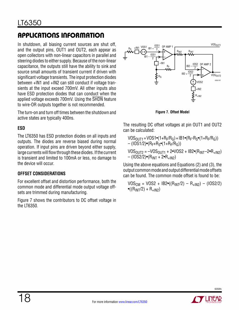
NOISE CONSIDERATIONS
A model showing the sources of output noise in the LT6350 is shown in Figure 8. The total output noise resulting from all contributors is governed by the equation:
The LT6350 uses very low noise op amps, resulting in a total differential output spot noise at 10kHz of 8.2nV/√Hz when the LT6350 is in the noninverting gain-of-two con-figuration shown in Figure 2. This is equivalent to the voltage noise of a 1015Ω resistor at the +IN1 input. For source resistors larger than about 1k, voltage noise due to the source resistance will start to dominate output noise. Source resistors larger than about 13k will interact with the input current noise and result in output noise that is resistor noise and amplifier current noise dominant.
–+
+–
RG
RS
R+IN2
RF
RINT RINT
in1
in1
en1
enRF
enRG
enRS
eno1
eno2
–IN1
+IN1
+IN2
OP AMP 1
OP AMP 2
6350 F08
enRINT enRINT
en2
enR+IN2
in2
in2
+
eno
–
Figure 8. Noise Model
Note that the parallel combination of gain-setting resis-tors RF and RG behaves like the source resistance, RS, from the point of view of noise calculations, and the value should be kept below about 1k to avoid increasing the output noise. Lower-value gain and feedback resistors,
eno = √(4 • [e2n1 + (in1RS)2 + e2
nRS](1 + (RF /RG))2 + 4 • (in1RF)2 + 4e2nRF (1 + (RF /RG)) + 4e2
n2 + 4e2nR+IN2 +
2e2nRINT + (in2RINT)2 + 4 • (in2R+IN2)2 )
LT6350
206350fc
For more information www.linear.com/LT6350
applicaTions inForMaTionRG and RF, will always result in lower output noise at the expense of increased distortion due to increased loading of op amp 1. Note that op amp 1 is loaded internally by the 1k input resistor to op amp 2, and therefore external loading should not be much heavier than 1k to avoid degrading distortion performance.
When using RF equal to RS (for low offsets) in the gain-of-two configuration, wideband noise can be substantially reduced by bypassing across RF. For lowest output noise always bypass at the +IN2 pin with a capacitor of at least 0.1µF as seen in the Typical Application schematic on the front page. Alternatively, for systems that can tolerate output voltage offsets, omitting R+IN2 and RF will mini-mize output noise at the expense of larger output offset voltage.
Using a single pole passive RC filter network at the output of the LT6350, as shown in Figure 6, reduces the output noise bandwidth and thereby increases the signal-to-noise ratio of the system. For example, in a typical system with output signals of 8VP-P, and a signal bandwidth of 100kHz, an RC output filter with RFILT = 100Ω and CDIFF = 6.8nF, slightly increases the output spot noise from 8.2nV√Hz to 8.4nV√Hz, but will reduce the total integrated noise from 47µV (33MHz noise bandwidth) to 3.6µV (184kHz noise bandwidth) and improve the SNR from 96dB to 118dB. Keep in mind that long RC time constants in the output filter can increase the settling time at the inputs of the ADC; incomplete settling can cause gain errors or increase apparent crosstalk in multiplexed systems.
OUTPUT PHASE BALANCE
The topology of the LT6350 is that of a noninverting stage followed by an inverting stage. This topology presents a high impedance single-ended input and provides low impedance differential outputs. The output of the inverting buffer, OUT2, is slightly delayed with respect to the output of the noninverting buffer, OUT1. In the LT6350, the delay from OUT1 to OUT2 over an input bandwidth from DC to the differential f–3dB frequency is a nearly constant 6.8ns, as shown in the group delay plot in the Typical Performance Characteristics section of this data sheet. The delay is equivalent to a small phase offset from the nominal 180° phase of the differential outputs. The size of the phase offset grows with frequency. The phase imbalance causes a small frequency-dependent common mode component to appear at the outputs. A practical measure of this effect can be found in the balance specification, which is defined to be the change in output common mode level caused by the presence of an output differential signal:
Balance ≡ ((VOUTDIFF/VIN)/(VOUTCM/VIN))
The balance of the LT6350 at any frequency, f, can be approximated from the delay, td, between outputs:
Balance (dB) ≅ 20 • log((4)/(2 • π • f • td))
The approximation is very good from low frequencies up to frequencies where the balance approaches 20dB, about 10MHz for the LT6350. At DC, the balance is limited by the matching of the internal resistors that set the gain in the inverting buffer. 1% matching of the resistors limits the balance to 52dB at DC. At frequencies near the f–3dB point of the differential transfer function, additional phase lag and gain rolloff also contribute to balance. See the balance plot in the Typical Performance Characteristics for a detailed picture of Balance vs Input Frequency.
LT6350
216350fc
For more information www.linear.com/LT6350
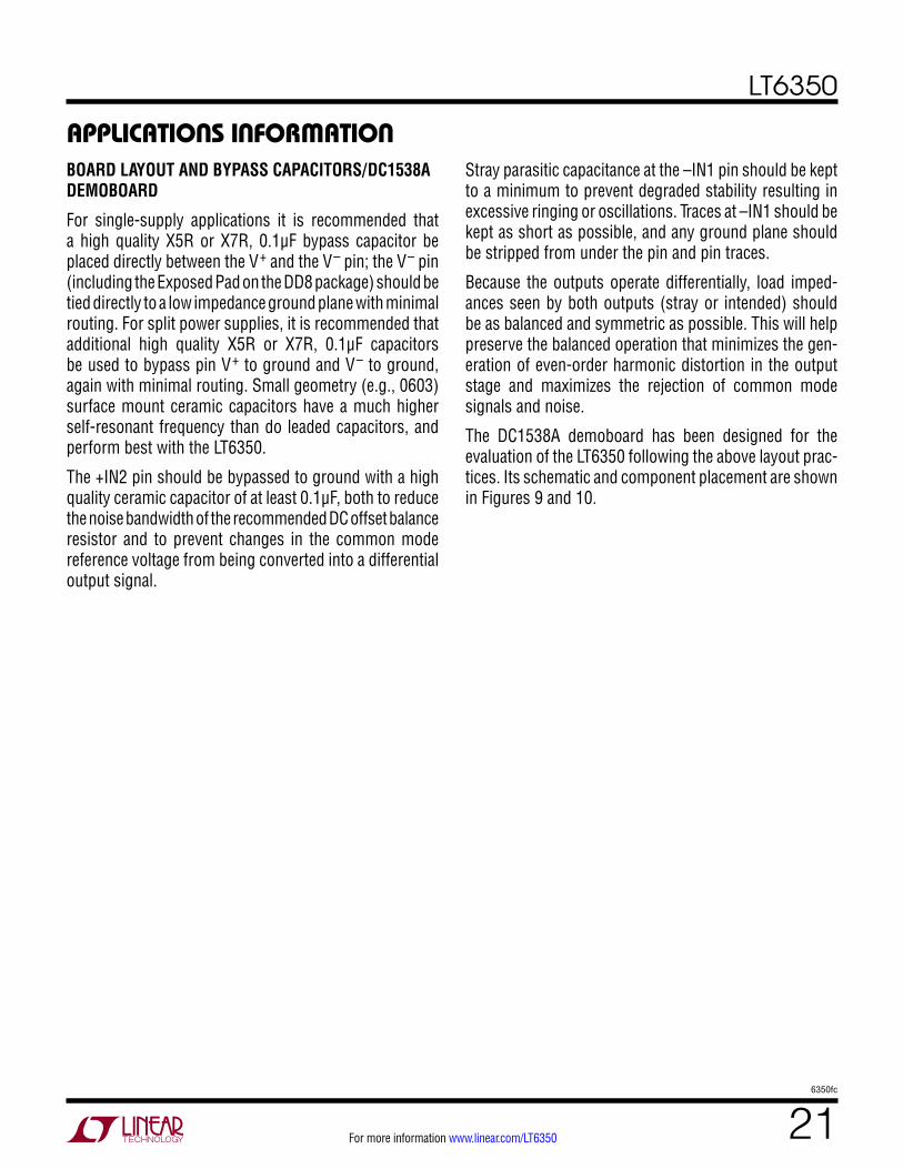
applicaTions inForMaTionBOARD LAYOUT AND BYPASS CAPACITORS/DC1538A DEMOBOARD
For single-supply applications it is recommended that a high quality X5R or X7R, 0.1μF bypass capacitor be placed directly between the V+ and the V– pin; the V– pin (including the Exposed Pad on the DD8 package) should be tied directly to a low impedance ground plane with minimal routing. For split power supplies, it is recommended that additional high quality X5R or X7R, 0.1μF capacitors be used to bypass pin V+ to ground and V– to ground, again with minimal routing. Small geometry (e.g., 0603) surface mount ceramic capacitors have a much higher self-resonant frequency than do leaded capacitors, and perform best with the LT6350.
The +IN2 pin should be bypassed to ground with a high quality ceramic capacitor of at least 0.1μF, both to re duce the noise bandwidth of the recommended DC offset balance resistor and to prevent changes in the common mode reference voltage from being converted into a dif ferential output signal.
Stray parasitic capacitance at the –IN1 pin should be kept to a minimum to prevent degraded stability resulting in excessive ringing or oscillations. Traces at –IN1 should be kept as short as possible, and any ground plane should be stripped from under the pin and pin traces.
Because the outputs operate differentially, load imped-ances seen by both outputs (stray or intended) should be as balanced and symmetric as possible. This will help preserve the balanced operation that minimizes the gen-eration of even-order harmonic distortion in the output stage and maximizes the rejection of common mode signals and noise.
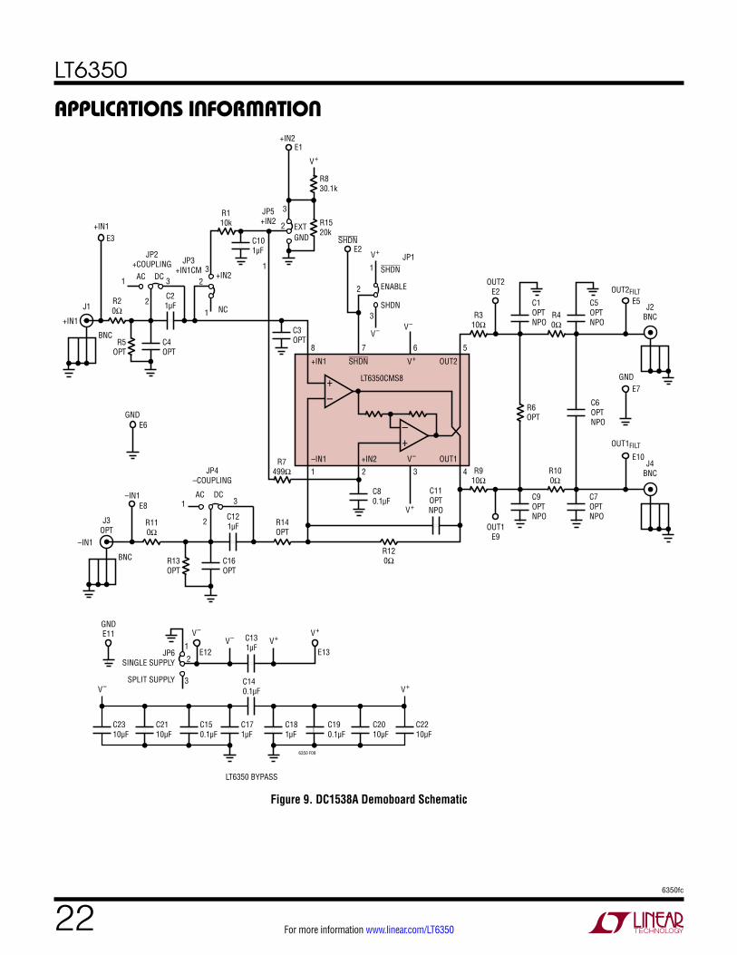
The DC1538A demoboard has been designed for the evaluation of the LT6350 following the above layout prac-tices. Its schematic and component placement are shown in Figures 9 and 10.
LT6350
226350fc
For more information www.linear.com/LT6350
applicaTions inForMaTion
+IN1
+IN1E3
J1R20Ω
C21µF
BNCR5
OPTC4OPT
JP2+COUPLING
AC DC1
1
1 1
33
3
3
2
2
22
JP3+IN1CM
JP5+IN2
C3OPT
R14OPT
R7499Ω
NC
R110k R15
20k
R830.1k
+IN2
+IN2E1
SHDN
JP1V+
V+
V–
V+
V–
SHDN
ENABLE
LT6350CMS8
SHDNR3
10Ω
R910Ω
R40Ω
R100Ω
E5
E7
E10
J2BNC
J4BNC
OUT2E2
OUT1E9
C1OPTNPO
C5OPTNPO
C6OPTNPO
R6OPT
C7OPTNPO
C9OPTNPO
OUT2FILT
OUT1FILT
GND
GNDE6
–IN1
–IN1
E8
J3OPT
BNC
R110Ω
JP4–COUPLING
AC DC1 3
2 C121µF
C80.1µF
C16OPT
R13OPT
C11OPTNPO
R120Ω
V+
V–
+IN1
–IN1 +IN2
SHDN OUT2
OUT1
+–
+–
C101µF
E13
C131µF
C140.1µF
C171µF
C150.1µF
C181µF
C190.1µF
C2010µF
C2210µF
GNDE11
E12
V– V+
V+V–
V– V+
LT6350 BYPASS
6350 F09
8 7 6 5
1 2 3 4
E2
EXTGND
C2110µF
C2310µF
1
2
3
JP6SINGLE SUPPLY
SPLIT SUPPLY
Figure 9. DC1538A Demoboard Schematic
LT6350
236350fc
For more information www.linear.com/LT6350
applicaTions inForMaTion
Figure 10. DC1538A Demoboard Layout
LT6350
246350fc
For more information www.linear.com/LT6350
Figure 11. DC1539A Demoboard Layout
applicaTions inForMaTion
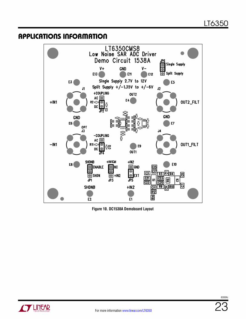
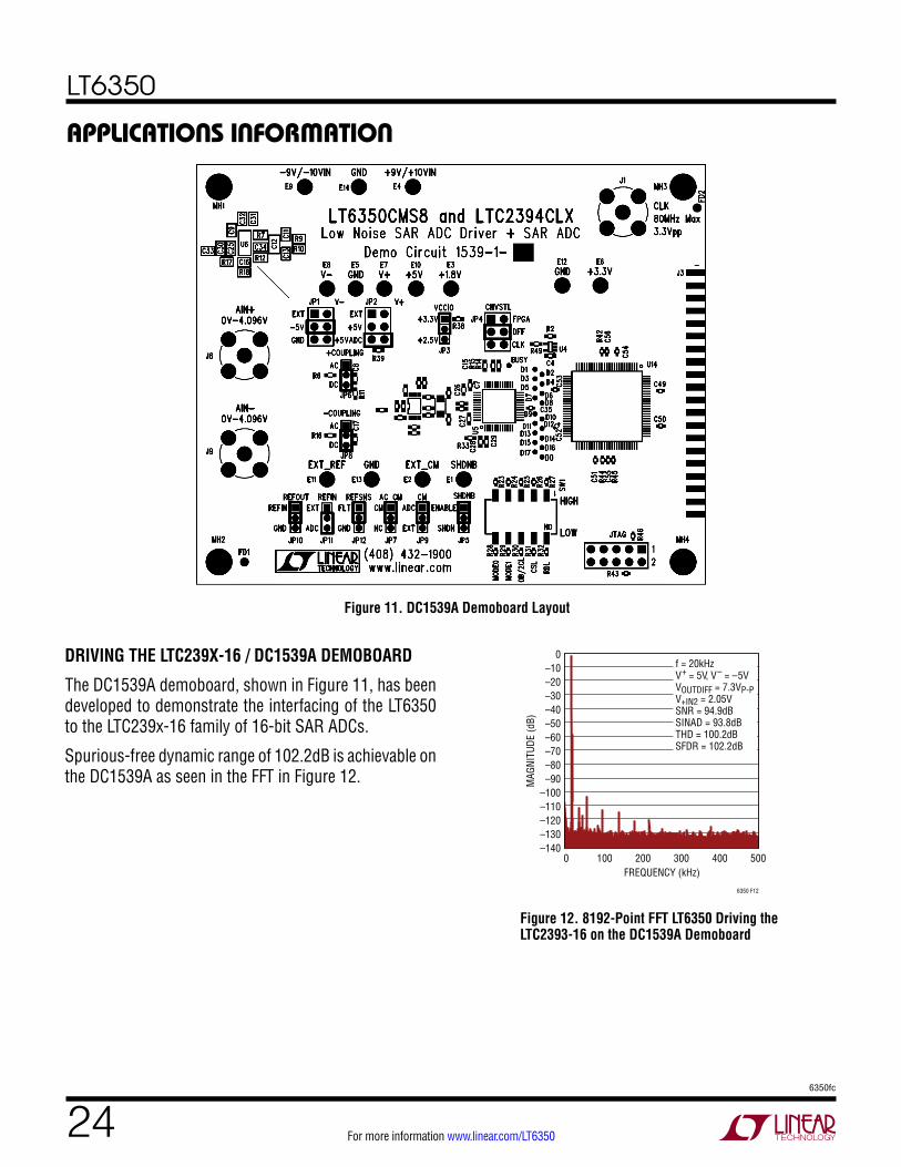
DRIVING THE LTC239X-16 / DC1539A DEMOBOARD
The DC1539A demoboard, shown in Figure 11, has been developed to dem onstrate the interfacing of the LT6350 to the LTC239x-16 family of 16-bit SAR ADCs.
Spurious-free dynamic range of 102.2dB is achievable on the DC1539A as seen in the FFT in Figure 12.
Figure 12. 8192-Point FFT LT6350 Driving the LTC2393-16 on the DC1539A Demoboard
FREQUENCY (kHz)0
–140
MAG
NITU
DE (d
B)
–30
–10–20
–60–50–40
–70–80–90
–110–100
–120–130
0
100 200 500300
6350 F12
400
f = 20kHzV+ = 5V, V– = –5VVOUTDIFF = 7.3VP-PV+IN2 = 2.05VSNR = 94.9dBSINAD = 93.8dBTHD = 100.2dBSFDR = 102.2dB
LT6350
256350fc
For more information www.linear.com/LT6350
+–
+IN1
–IN1
V+
V–
OUT2
OUT1
SHDN
+IN2
5V
2.5V
499Ω
8 7 3 5
1 2 6 4
0.1µF
0.1µF
2.5V
1000pF
R3523Ω
LT6350
6350 F13
+–
VOUT1
VOUT2
C51000pF
4750Ω0.01µFVIN+–
174Ω 2210Ω
Figure 13. 100KHz, 3rd Order Butterworth Filter
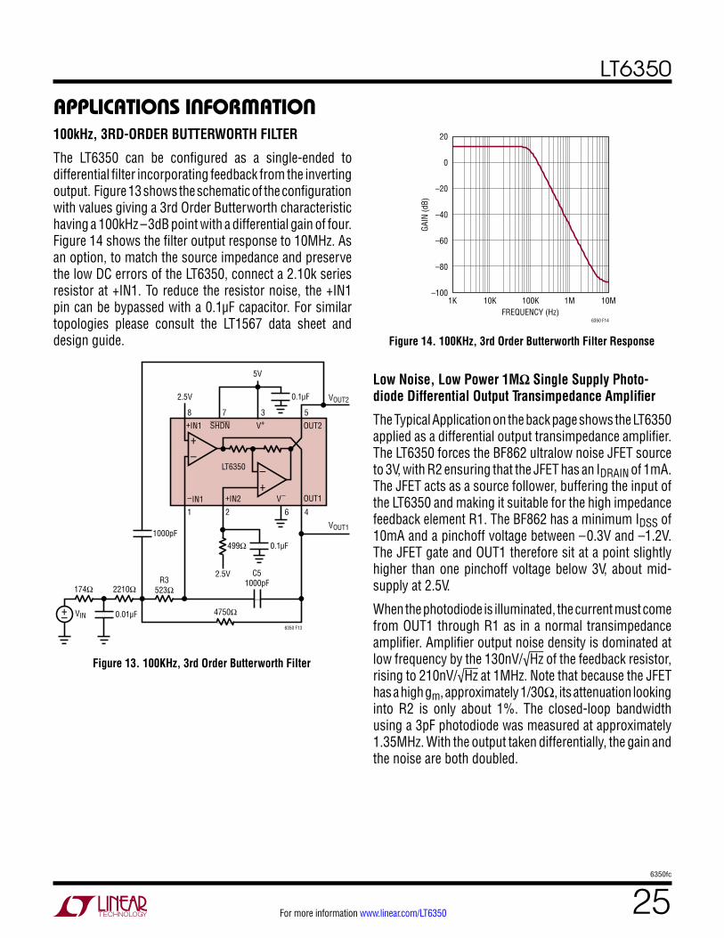
applicaTions inForMaTion100kHz, 3RD-ORDER BUTTERWORTH FILTER
The LT6350 can be configured as a single-ended to differential filter incorporating feedback from the inverting output. Figure 13 shows the schematic of the configuration with values giving a 3rd Order Butterworth characteristic having a 100kHz –3dB point with a differential gain of four. Figure 14 shows the filter output response to 10MHz. As an option, to match the source impedance and preserve the low DC errors of the LT6350, connect a 2.10k series resistor at +IN1. To reduce the resistor noise, the +IN1 pin can be bypassed with a 0.1µF capacitor. For similar topologies please consult the LT1567 data sheet and design guide.
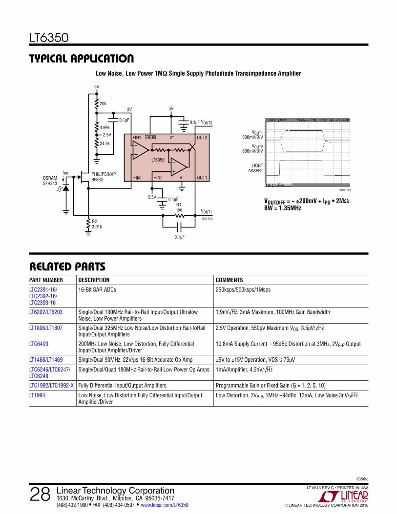
Low Noise, Low Power 1MΩ Single Supply Photo-diode Differential Output Transimpedance Amplifier
The Typical Application on the back page shows the LT6350 applied as a differential output transimpedance amplifier. The LT6350 forces the BF862 ultralow noise JFET source to 3V, with R2 ensuring that the JFET has an IDRAIN of 1mA. The JFET acts as a source follower, buffering the input of the LT6350 and making it suitable for the high impedance feedback element R1. The BF862 has a minimum IDSS of 10mA and a pinchoff voltage between –0.3V and –1.2V. The JFET gate and OUT1 therefore sit at a point slightly higher than one pinchoff voltage below 3V, about mid-supply at 2.5V.
When the photodiode is illuminated, the current must come from OUT1 through R1 as in a normal transimpedance amplifier. Amplifier output noise density is dominated at low frequency by the 130nV/√Hz of the feedback resistor, rising to 210nV/√Hz at 1MHz. Note that because the JFET has a high gm, approximately 1/30Ω, its attenuation looking into R2 is only about 1%. The closed-loop bandwidth using a 3pF photodiode was measured at approximately 1.35MHz. With the output taken differentially, the gain and the noise are both doubled.
Figure 14. 100KHz, 3rd Order Butterworth Filter Response
FREQUENCY (Hz)1K
GAIN
(dB)
20
–60
–40
–80
–20
0
–100100K 1M
6350 F14
10M10K
LT6350
266350fc
For more information www.linear.com/LT6350
package DescripTion
MSOP (MS8) 0307 REV F
0.53 ± 0.152(.021 ± .006)
SEATINGPLANE
NOTE:1. DIMENSIONS IN MILLIMETER/(INCH)2. DRAWING NOT TO SCALE3. DIMENSION DOES NOT INCLUDE MOLD FLASH, PROTRUSIONS OR GATE BURRS. MOLD FLASH, PROTRUSIONS OR GATE BURRS SHALL NOT EXCEED 0.152mm (.006") PER SIDE4. DIMENSION DOES NOT INCLUDE INTERLEAD FLASH OR PROTRUSIONS. INTERLEAD FLASH OR PROTRUSIONS SHALL NOT EXCEED 0.152mm (.006") PER SIDE5. LEAD COPLANARITY (BOTTOM OF LEADS AFTER FORMING) SHALL BE 0.102mm (.004") MAX
0.18(.007)
0.254(.010)
1.10(.043)MAX
0.22 – 0.38(.009 – .015)
TYP
0.1016 ± 0.0508(.004 ± .002)
0.86(.034)REF
0.65(.0256)
BSC
0° – 6° TYP
DETAIL “A”
DETAIL “A”
GAUGE PLANE
1 2 3 4
4.90 ± 0.152(.193 ± .006)
8 7 6 5
3.00 ± 0.102(.118 ± .004)
(NOTE 3)
3.00 ± 0.102(.118 ± .004)
(NOTE 4)
0.52(.0205)
REF
5.23(.206)MIN
3.20 – 3.45(.126 – .136)
0.889 ± 0.127(.035 ± .005)
RECOMMENDED SOLDER PAD LAYOUT
0.42 ± 0.038(.0165 ± .0015)
TYP
0.65(.0256)
BSC
DD Package8-Lead Plastic DFN (3mm × 3mm)
(Reference LTC DWG # 05-08-1698 Rev C)
3.00 ±0.10(4 SIDES)
NOTE:1. DRAWING TO BE MADE A JEDEC PACKAGE OUTLINE M0-229 VARIATION OF (WEED-1)2. DRAWING NOT TO SCALE3. ALL DIMENSIONS ARE IN MILLIMETERS4. DIMENSIONS OF EXPOSED PAD ON BOTTOM OF PACKAGE DO NOT INCLUDE MOLD FLASH. MOLD FLASH, IF PRESENT, SHALL NOT EXCEED 0.15mm ON ANY SIDE
5. EXPOSED PAD SHALL BE SOLDER PLATED6. SHADED AREA IS ONLY A REFERENCE FOR PIN 1 LOCATION ON TOP AND BOTTOM OF PACKAGE
0.40 ± 0.10
BOTTOM VIEW—EXPOSED PAD
1.65 ± 0.10(2 SIDES)
0.75 ±0.05
R = 0.125TYP
2.38 ±0.10
14
85
PIN 1TOP MARK
(NOTE 6)
0.200 REF
0.00 – 0.05
(DD8) DFN 0509 REV C
0.25 ± 0.05
2.38 ±0.05
RECOMMENDED SOLDER PAD PITCH AND DIMENSIONSAPPLY SOLDER MASK TO AREAS THAT ARE NOT SOLDERED
1.65 ±0.05(2 SIDES)2.10 ±0.05
0.50BSC
0.70 ±0.05
3.5 ±0.05
PACKAGEOUTLINE
0.25 ± 0.050.50 BSC
MS8 Package8-Lead Plastic MSOP
(Reference LTC DWG # 05-08-1660 Rev F)
LT6350
276350fc
For more information www.linear.com/LT6350
Information furnished by Linear Technology Corporation is believed to be accurate and reliable. However, no responsibility is assumed for its use. Linear Technology Corporation makes no representa-tion that the interconnection of its circuits as described herein will not infringe on existing patent rights.
revision hisToryREV DATE DESCRIPTION PAGE NUMBER
A 03/10 Updated Units on VOH in Electrical Characteristics 4
B 05/10 Updated Note 2Updated Related Parts
528
C 06/13 Corrected curve labels on Input Bias Current vs Input Voltage graphs 7
LT6350
286350fc
For more information www.linear.com/LT6350 LINEAR TECHNOLOGY CORPORATION 2010
LT 0613 REV C • PRINTED IN USALinear Technology Corporation1630 McCarthy Blvd., Milpitas, CA 95035-7417(408) 432-1900 ● FAX: (408) 434-0507 ● www.linear.com/LT6350
relaTeD parTs
Typical applicaTion
PART NUMBER DESCRIPTION COMMENTS
LTC2391-16/LTC2392-16/LTC2393-16
16-Bit SAR ADCs 250ksps/500ksps/1Msps
LT6202/LT6203 Single/Dual 100MHz Rail-to-Rail Input/Output Ultralow Noise, Low Power Amplifiers
1.9nV√Hz, 3mA Maximum, 100MHz Gain Bandwidth
LT1806/LT1807 Single/Dual 325MHz Low Noise/Low Distortion Rail-toRail Input/Output Amplifiers
2.5V Operation, 550µV Maximum VOS, 3.5µV/√Hz
LTC6403 200MHz Low Noise, Low Distortion, Fully Differential Input/Output Amplifier/Driver
10.8mA Supply Current, –95dBc Distortion at 3MHz, 2VP-P Output
LT1468/LT1469 Single/Dual 90MHz, 22V/µs 16-Bit Accurate Op Amp ±5V to ±15V Operation, VOS ≤ 75µV
LTC6246/LTC6247/LTC6248
Single/Dual/Quad 180MHz Rail-to-Rail Low Power Op Amps 1mA/Amplifier, 4.2nV/√Hz
LTC1992/LTC1992-X Fully Differential Input/Output Amplifiers Programmable Gain or Fixed Gain (G = 1, 2, 5, 10)
LT1994 Low Noise, Low Distortion Fully Differential Input/Output Amplifier/Driver
Low Distortion, 2VP-P, 1MHz –94dBc, 13mA, Low Noise 3nV/√Hz
+–
+IN1
–IN1
V+
V–
OUT2
OUT1
SHDN
+IN2
5V3V
R23.01k
R11M
20k
24.9k
5V
0.1µF0.1µF
0.1µF2.5V
LT6350
PHILIPS/NXPBF862
6350 TA03
+–
VOUT1
IPD
VOUT24.99k
2.5V
0.1pF
OSRAMSFH213
Low Noise, Low Power 1MΩ Single Supply Photodiode Transimpedance Amplifier
VOUT1500mV/DIV
VOUT2500mV/DIV
LIGHTASSERT
6350 TA04
VOUTDIFF = ~ ±200mV + IPD • 2MΩ BW = 1.35MHz