logic families
TRANSCRIPT
Logic Families The types of digital circuit devices are classified in
families that based on the specific circuit technology. Among them, the most important are TTL and CMOS TTL (Transistor-Transistor Logic), made of bipolar transistors
It is called transistor–transistor logic because the logic function (e.g., AND) and amplification is performed by transistors
CMOS (Complementary Metal Oxide Semiconductor) made from MOSFET transistors
In the modern world, CMOS is the dominate technology used to construct digital circuit components, especially large-scale integrated circuits
The logic families differ from each other primarily in output current capability, power dissipation, propagation delay time, and operating power supply voltage
Characteristics of an Ideal Logic Family
The ideal logic family should have or be: Low power High speed Easy to use Many different logic functions Clear voltage levels for 0 (LOW) and 1 (HIGH)
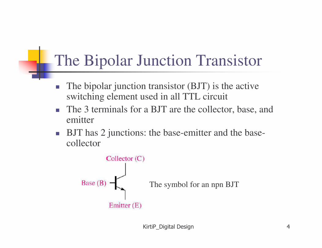
The Bipolar Junction Transistor The bipolar junction transistor (BJT) is the active
switching element used in all TTL circuit The 3 terminals for a BJT are the collector, base, and
emitter BJT has 2 junctions: the base-emitter and the base-
collector
The symbol for an npn BJT
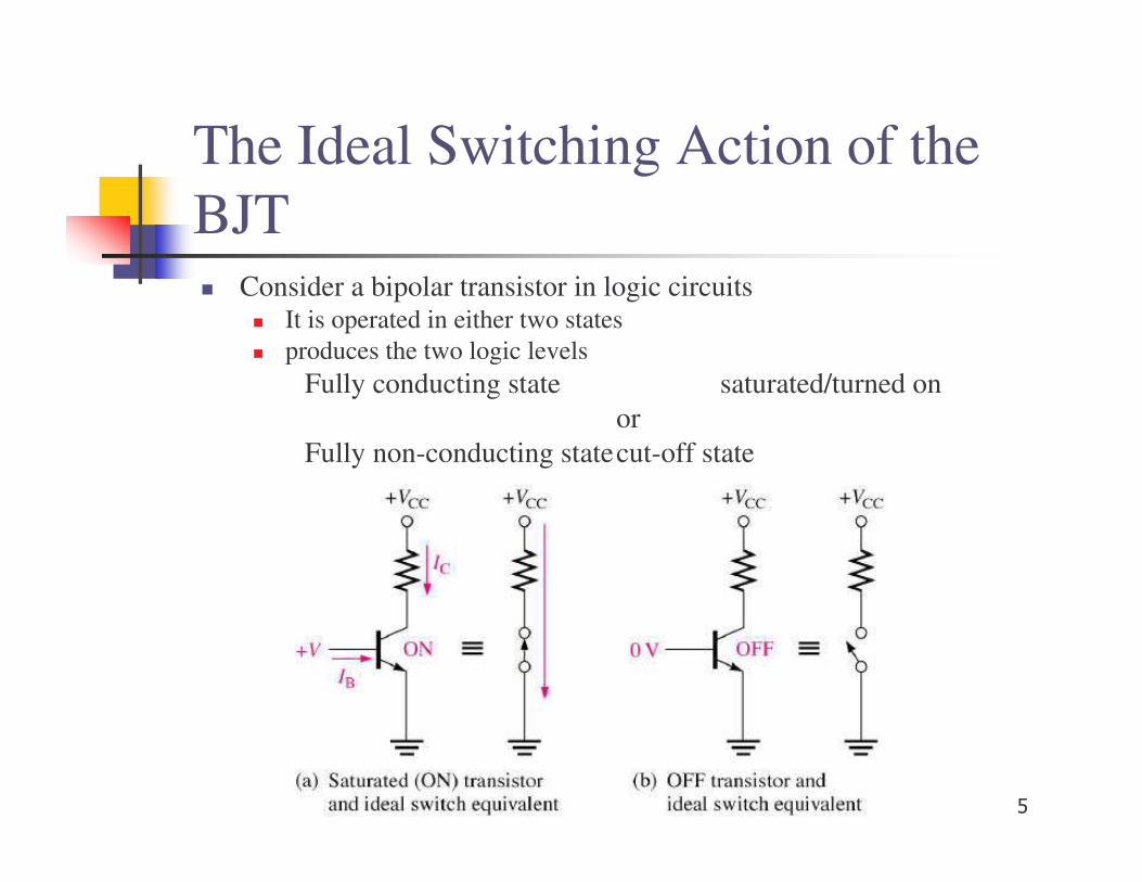
The Ideal Switching Action of the BJT Consider a bipolar transistor in logic circuits
It is operated in either two states produces the two logic levels
Fully conducting state saturated/turned onor
Fully non-conducting statecut-off state
Transistor-Transistor Logic In Transistor-Transistor logic or just TTL, logic gates are built only
around transistors TTL was developed in 1965 Through the years basic TTL has been improved to meet performance
requirements. There are many versions or families of TTL. For example Standard TTL High Speed TTL (twice as fast, twice as much power) Low Power TTL (1/10 the speed, 1/10 the power of “standard" TTL) Schhottky TTL etc. (for high-frequency uses )
Here we will discuss only basic TTL. Typically, all TTL logic families have three configurations for outputs Totem pole output Open collector output Tristate output
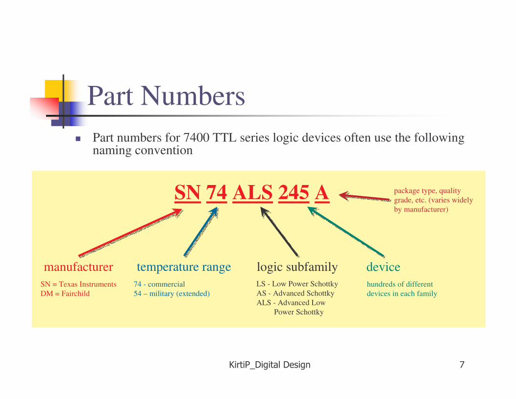
Part Numbers Part numbers for 7400 TTL series logic devices often use the following
naming convention
SN 74 ALS 245 A
manufacturer temperature range logic subfamily deviceLS - Low Power SchottkyAS - Advanced SchottkyALS - Advanced Low
Power Schottky
SN = Texas InstrumentsDM = Fairchild
74 - commercial54 – military (extended)
hundreds of different devices in each family
package type, quality grade, etc. (varies widely by manufacturer)
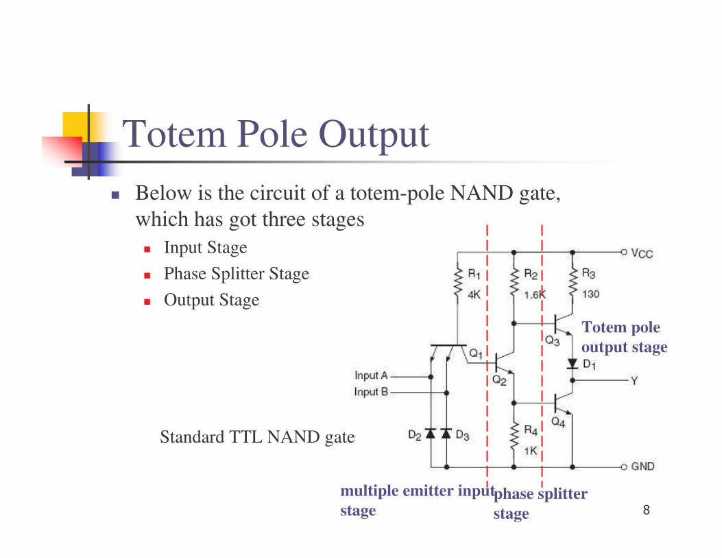
Totem Pole Output Below is the circuit of a totem-pole NAND gate,
which has got three stages Input Stage Phase Splitter Stage Output Stage
Standard TTL NAND gate
Totem pole output stage
phase splitter stage
multiple emitter input stage
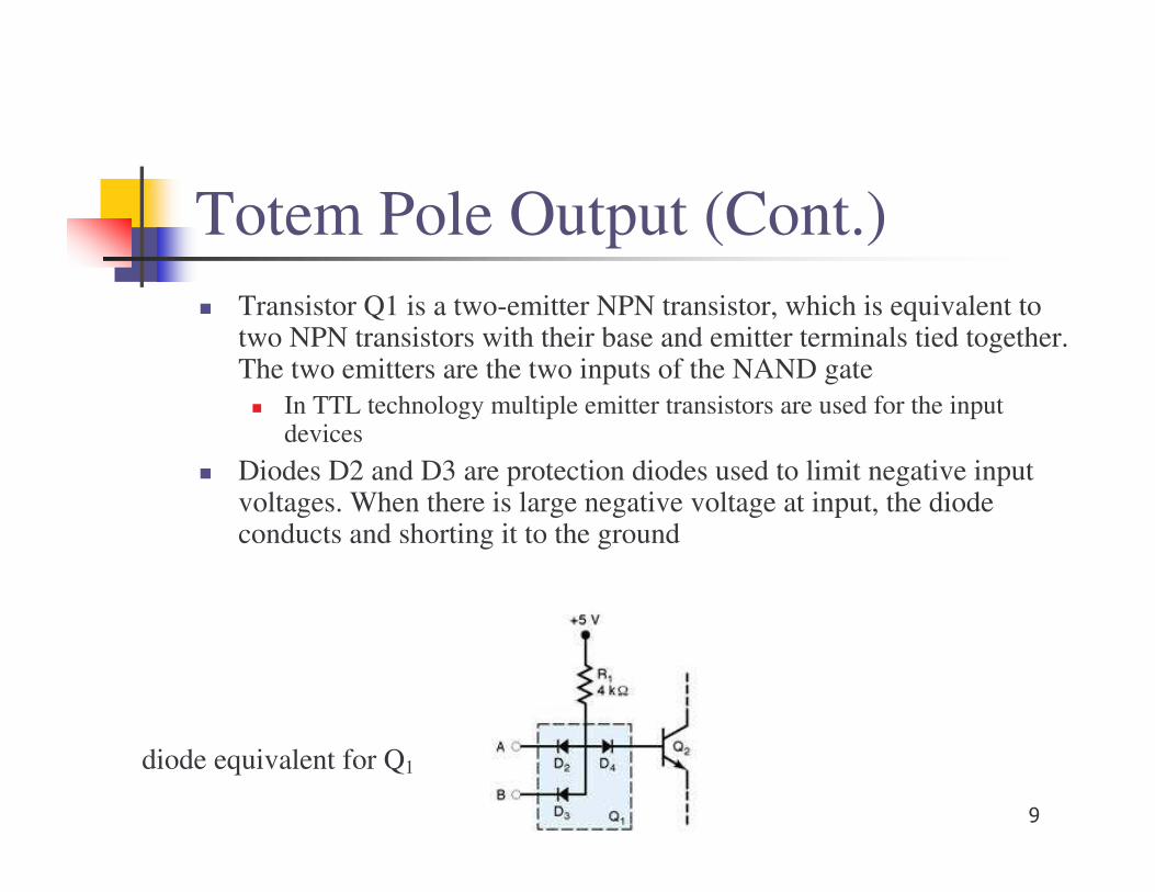
Totem Pole Output (Cont.) Transistor Q1 is a two-emitter NPN transistor, which is equivalent to
two NPN transistors with their base and emitter terminals tied together. The two emitters are the two inputs of the NAND gate In TTL technology multiple emitter transistors are used for the input
devices Diodes D2 and D3 are protection diodes used to limit negative input
voltages. When there is large negative voltage at input, the diode conducts and shorting it to the ground
diode equivalent for Q1
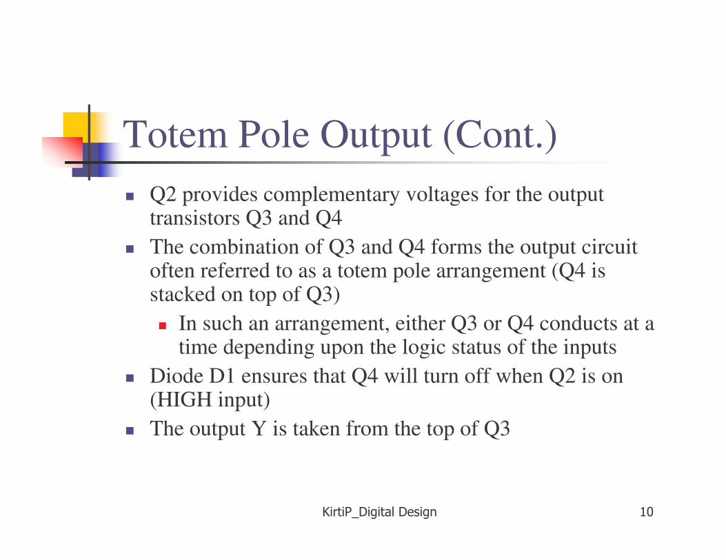
Totem Pole Output (Cont.) Q2 provides complementary voltages for the output
transistors Q3 and Q4 The combination of Q3 and Q4 forms the output circuit
often referred to as a totem pole arrangement (Q4 is stacked on top of Q3) In such an arrangement, either Q3 or Q4 conducts at a
time depending upon the logic status of the inputs Diode D1 ensures that Q4 will turn off when Q2 is on
(HIGH input) The output Y is taken from the top of Q3
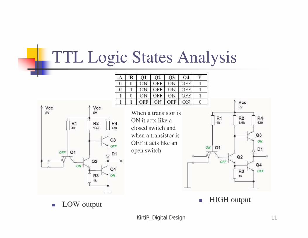
TTL Logic States Analysis
LOW output HIGH output
When a transistor is ON it acts like a closed switch and when a transistor is OFF it acts like an open switch
Advantages of Totem Pole Output Configuration
The features of this arrangement are Low power consumption Fast switching Low output impedance
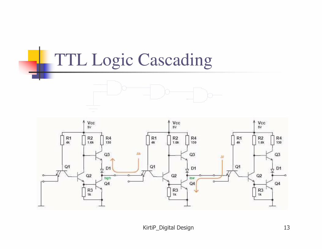
TTL Logic Cascading
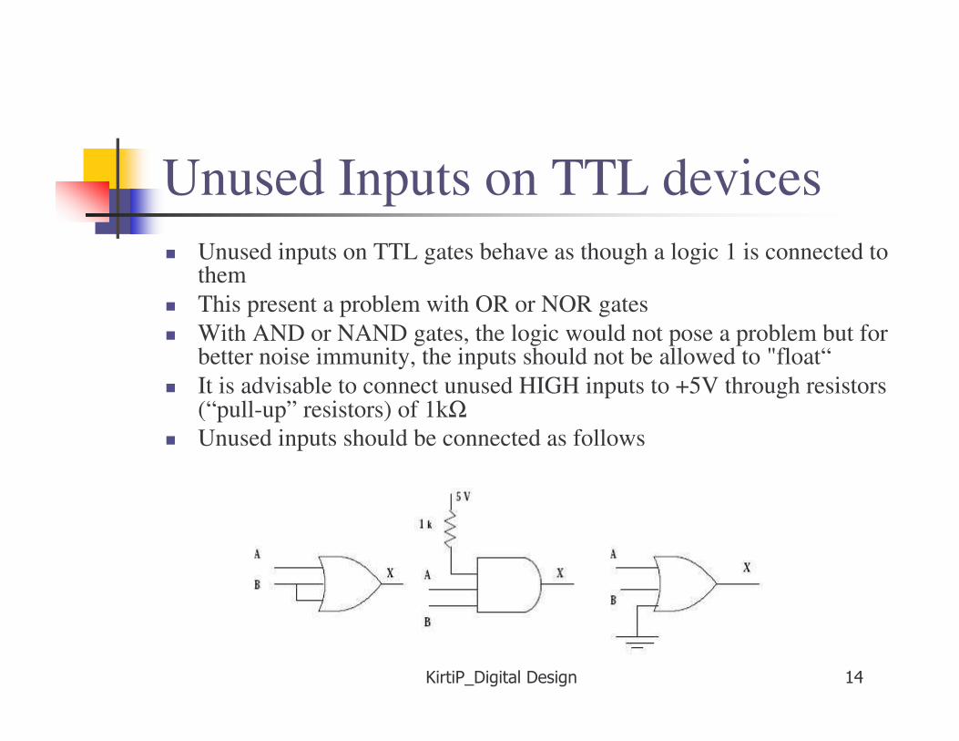
Unused Inputs on TTL devices Unused inputs on TTL gates behave as though a logic 1 is connected to
them This present a problem with OR or NOR gates With AND or NAND gates, the logic would not pose a problem but for
better noise immunity, the inputs should not be allowed to "float“ It is advisable to connect unused HIGH inputs to +5V through resistors
(“pull-up” resistors) of 1kΩ Unused inputs should be connected as follows
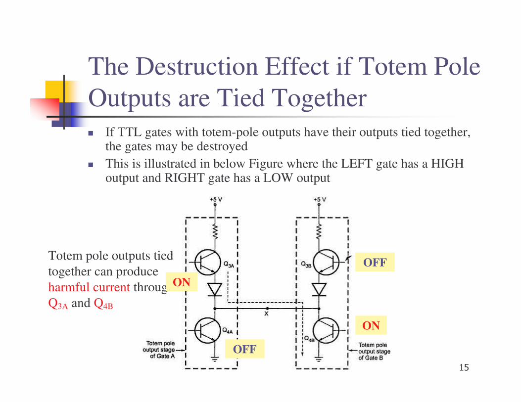
The Destruction Effect if Totem Pole Outputs are Tied Together If TTL gates with totem-pole outputs have their outputs tied together,
the gates may be destroyed This is illustrated in below Figure where the LEFT gate has a HIGH
output and RIGHT gate has a LOW output
Totem pole outputs tied together can produce harmful current throughQ3A and Q4B
ON
ON
OFF
OFF
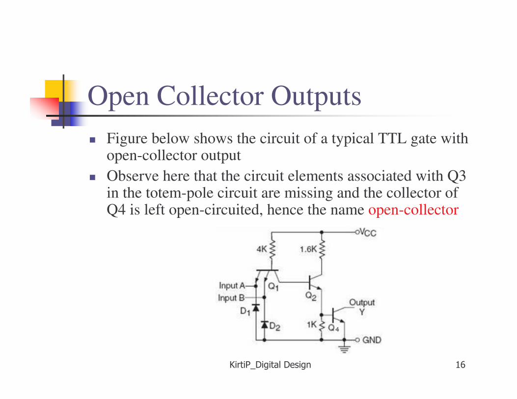
Open Collector Outputs Figure below shows the circuit of a typical TTL gate with
open-collector output Observe here that the circuit elements associated with Q3
in the totem-pole circuit are missing and the collector of Q4 is left open-circuited, hence the name open-collector
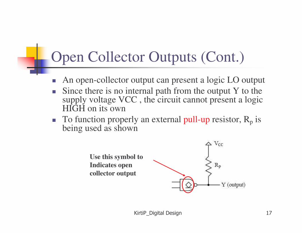
Open Collector Outputs (Cont.) An open-collector output can present a logic LO output Since there is no internal path from the output Y to the
supply voltage VCC , the circuit cannot present a logic HIGH on its own
To function properly an external pull-up resistor, Rp is being used as shown
Use this symbol to Indicates open collector output
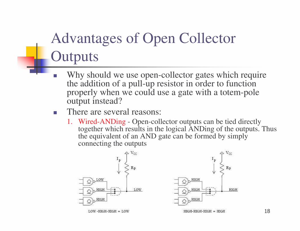
Advantages of Open Collector Outputs Why should we use open-collector gates which require
the addition of a pull-up resistor in order to function properly when we could use a gate with a totem-pole output instead?
There are several reasons:1. Wired-ANDing - Open-collector outputs can be tied directly
together which results in the logical ANDing of the outputs. Thus the equivalent of an AND gate can be formed by simply connecting the outputs
Advantages of Open Collector Outputs (Cont.)
2. Increased current levels - Standard TTL gates with totem-pole outputs can only provide a HIGH current output of 0.4 mA and a LOW current of 1.6 mA. Many open-collector gates have increased current ratings
3. Different voltage levels - A wide variety of output HIGH voltages can be achieved using open-collector gates. This is useful in interfacing different logic families that have different voltage and current level requirements
The big disadvantage of open-collector gates is their slow switching speed. This is because the value of pull-up resistor is in kΩ, which results in a relatively long time constants
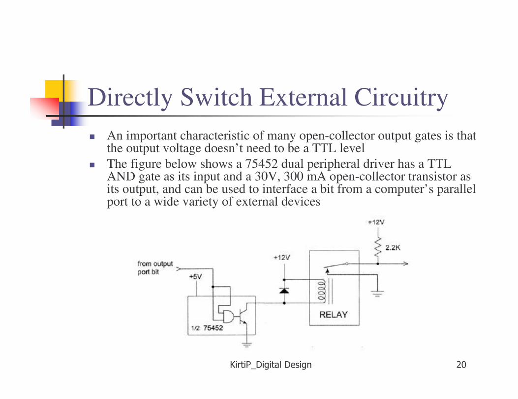
Directly Switch External Circuitry An important characteristic of many open-collector output gates is that
the output voltage doesn’t need to be a TTL level The figure below shows a 75452 dual peripheral driver has a TTL
AND gate as its input and a 30V, 300 mA open-collector transistor as its output, and can be used to interface a bit from a computer’s parallel port to a wide variety of external devices
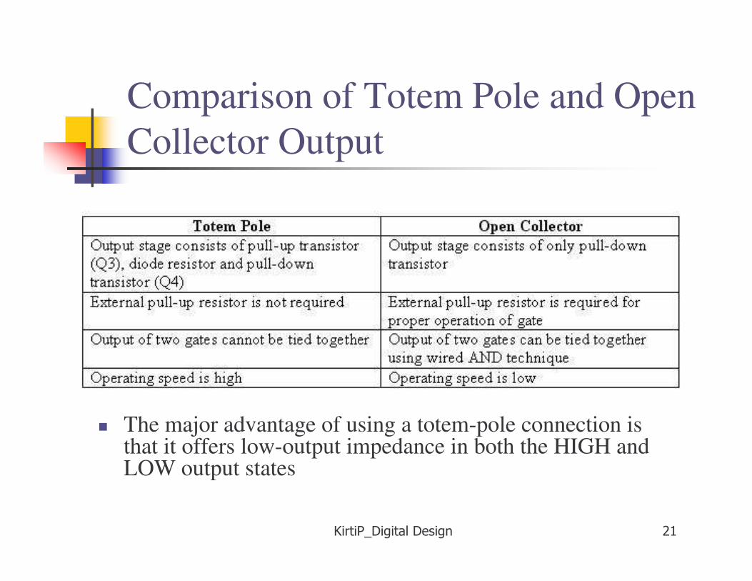
Comparison of Totem Pole and Open Collector Output
The major advantage of using a totem-pole connection is that it offers low-output impedance in both the HIGH and LOW output states
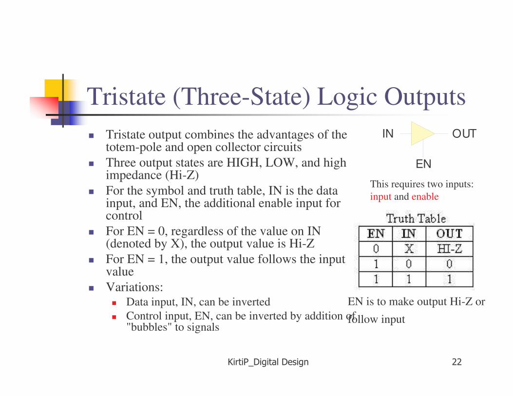
Tristate (Three-State) Logic Outputs Tristate output combines the advantages of the
totem-pole and open collector circuits Three output states are HIGH, LOW, and high
impedance (Hi-Z) For the symbol and truth table, IN is the data
input, and EN, the additional enable input for control
For EN = 0, regardless of the value on IN (denoted by X), the output value is Hi-Z
For EN = 1, the output value follows the input value
Variations: Data input, IN, can be inverted Control input, EN, can be inverted by addition of
"bubbles" to signals
IN OUT
EN
This requires two inputs: input and enable
EN is to make output Hi-Z or
follow input
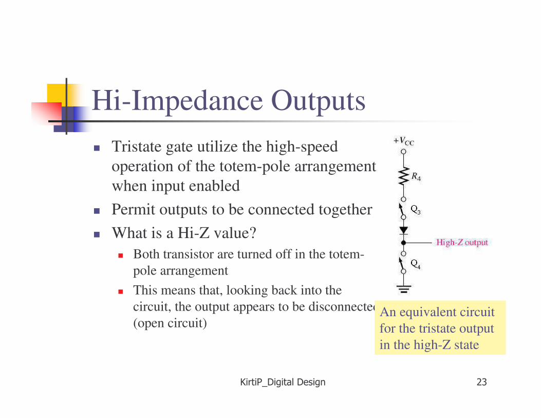
Hi-Impedance Outputs Tristate gate utilize the high-speed
operation of the totem-pole arrangement when input enabled
Permit outputs to be connected together What is a Hi-Z value?
Both transistor are turned off in the totem-pole arrangement
This means that, looking back into the circuit, the output appears to be disconnected (open circuit)
An equivalent circuit for the tristate output in the high-Z state
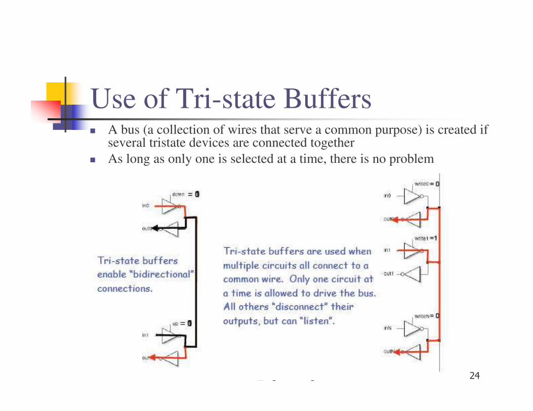
Use of Tri-state Buffers A bus (a collection of wires that serve a common purpose) is created if
several tristate devices are connected together As long as only one is selected at a time, there is no problem
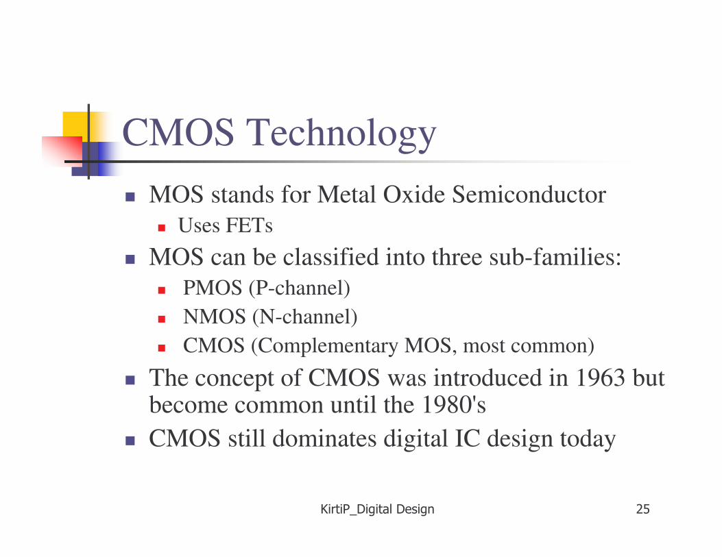
CMOS Technology MOS stands for Metal Oxide Semiconductor
Uses FETs MOS can be classified into three sub-families:
PMOS (P-channel) NMOS (N-channel) CMOS (Complementary MOS, most common)
The concept of CMOS was introduced in 1963 but become common until the 1980's
CMOS still dominates digital IC design today
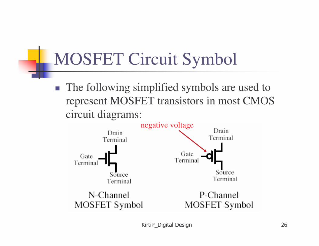
MOSFET Circuit Symbol The following simplified symbols are used to
represent MOSFET transistors in most CMOS circuit diagrams:
negative voltage
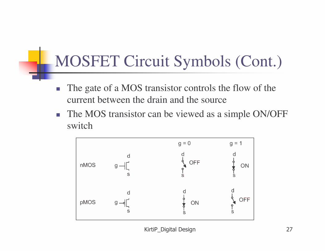
MOSFET Circuit Symbols (Cont.) The gate of a MOS transistor controls the flow of the
current between the drain and the source The MOS transistor can be viewed as a simple ON/OFF
switch
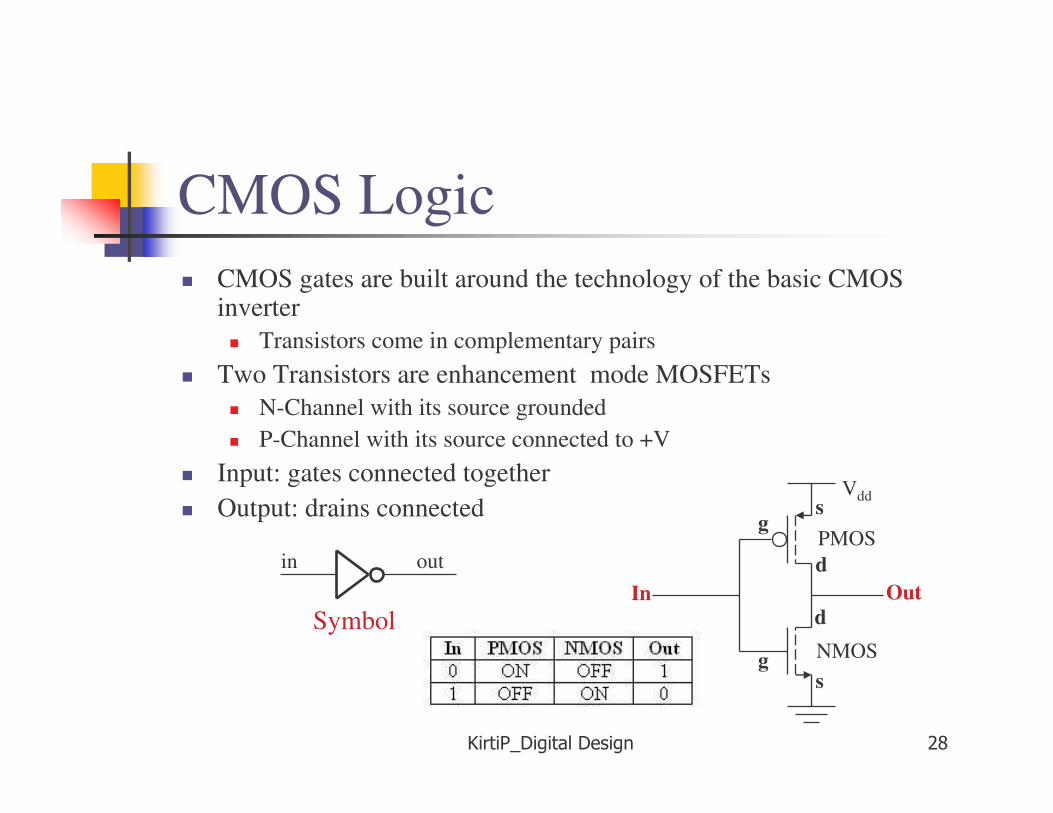
CMOS Logic CMOS gates are built around the technology of the basic CMOS
inverter Transistors come in complementary pairs
Two Transistors are enhancement mode MOSFETs N-Channel with its source grounded P-Channel with its source connected to +V
Input: gates connected together Output: drains connected
outin
Symbol
Vdd
OutIn
PMOS
NMOSs
s
d
d
g
g
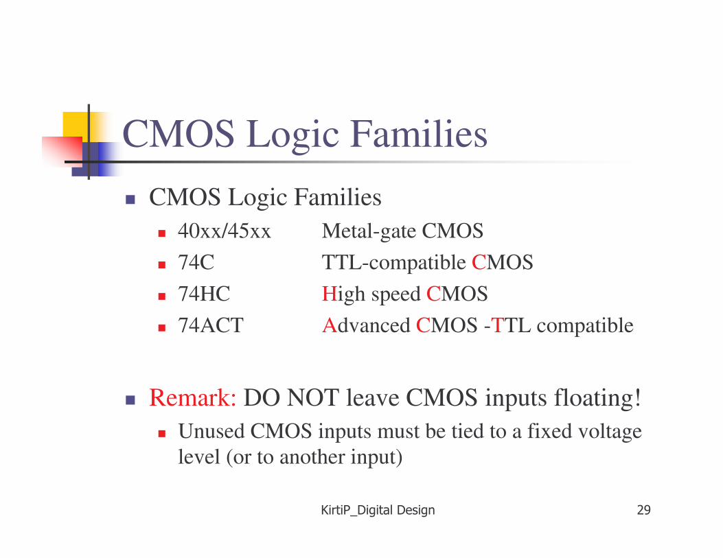
CMOS Logic Families CMOS Logic Families
40xx/45xx Metal-gate CMOS 74C TTL-compatible CMOS 74HC High speed CMOS 74ACT Advanced CMOS -TTL compatible
Remark: DO NOT leave CMOS inputs floating! Unused CMOS inputs must be tied to a fixed voltage
level (or to another input)
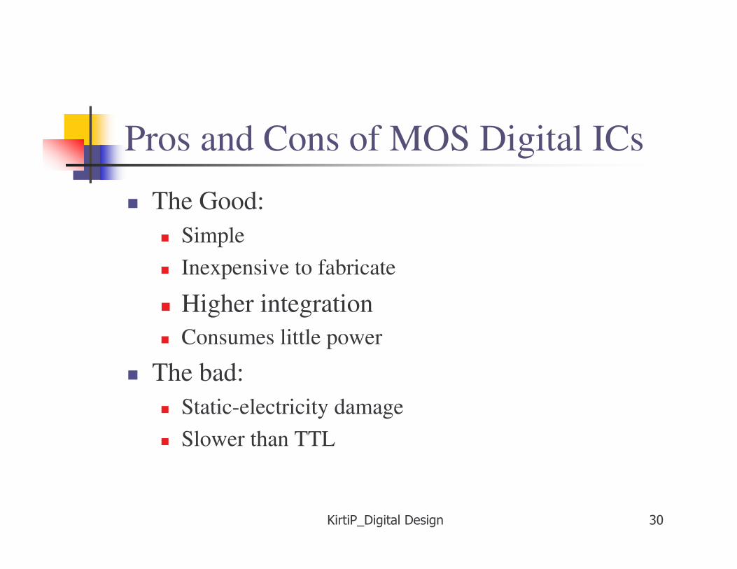
Pros and Cons of MOS Digital ICs
The Good: Simple Inexpensive to fabricate
Higher integration Consumes little power
The bad: Static-electricity damage Slower than TTL
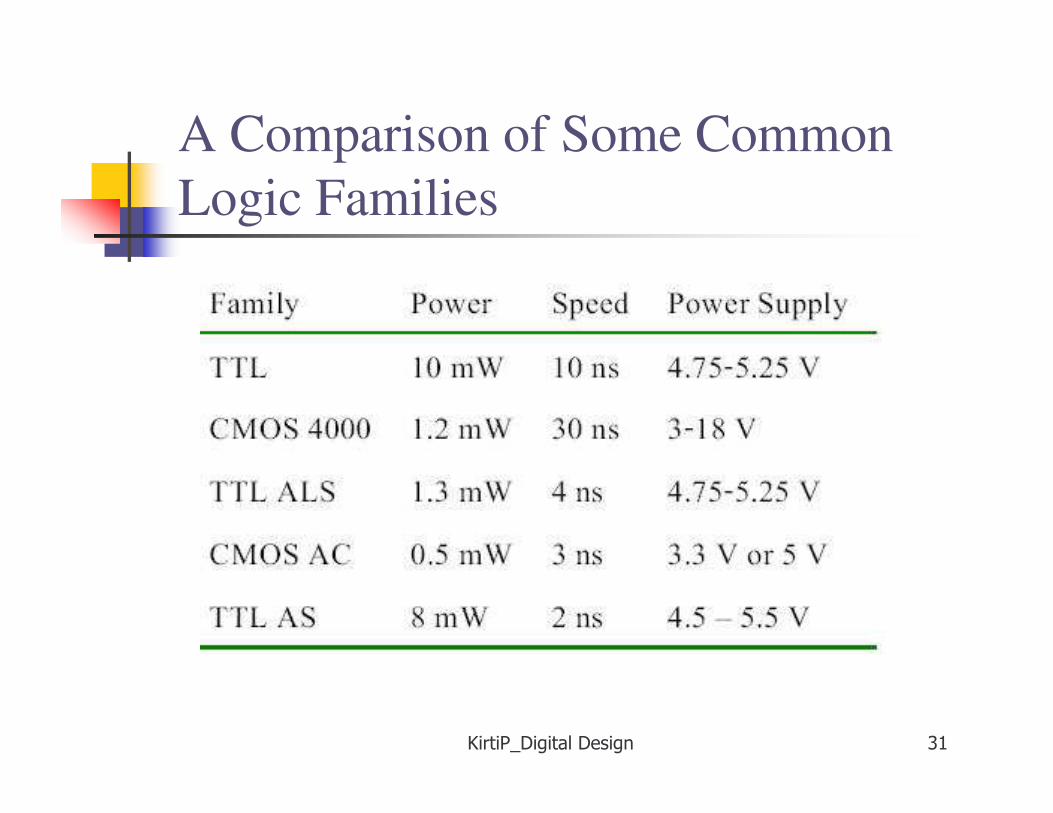
A Comparison of Some Common Logic Families
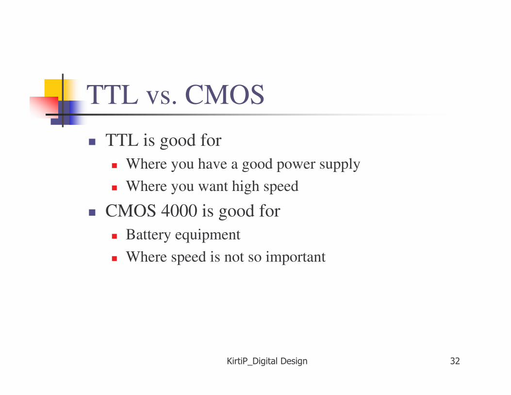
TTL vs. CMOS TTL is good for
Where you have a good power supply Where you want high speed
CMOS 4000 is good for Battery equipment Where speed is not so important