log periodic antenna design siti norhidayah binti...
TRANSCRIPT

LOG PERIODIC ANTENNA DESIGN
SITI NORHIDAYAH BINTI HJ. MOHAMED
This report is submitted in partial fulfillment of the requirements for the award of
Bachelor of Electronic Engineering (Telecommunication Electronics Engineering) With
Honours
Faculty of Elctronic and Computer Engineering
Universiti Teknikal Malaysia Melaka
May 2008

UNIVERSTI TEKNIKAL MALAYSIA MELAKA FAKULTI KEJURUTERAAN ELEKTRONIK DAN KEJURUTERAAN KOMPUTER
BORANG PENGESAHAN STATUS LAPORAN
PROJEK SARJANA MUDA II
Tajuk Projek : LOG PERIODIC ANTENNA DESIGN
Sesi
Pengajian : 2007/2008
Saya SITI NORHIDAYAH BINTI HJ. MOHAMED
mengaku membenarkan Laporan Projek Sarjana Muda ini disimpan di Perpustakaan dengan syarat-syarat kegunaan seperti berikut:
1. Laporan adalah hakmilik Universiti Teknikal Malaysia Melaka.
2. Perpustakaan dibenarkan membuat salinan untuk tujuan pengajian sahaja.
3. Perpustakaan dibenarkan membuat salinan laporan ini sebagai bahan pertukaran antara institusi
pengajian tinggi.
4. Sila tandakan ( √ ) :
SULIT*
(Mengandungi maklumat yang berdarjah keselamatan atau kepentingan Malaysia seperti yang termaktub di dalam AKTA RAHSIA RASMI 1972)
TERHAD*
(Mengandungi maklumat terhad yang telah ditentukan oleh organisasi/badan di mana penyelidikan dijalankan)
TIDAK TERHAD
Disahkan oleh:
__________________________ ___________________________________ (TANDATANGAN PENULIS) (COP DAN TANDATANGAN PENYELIA)
Alamat Tetap: NO. 243-A RPT KAMPUNG
CHENULANG, 18000 KUALA KRAI, KELANTAN.
Tarikh: 02 MAY 2008 Tarikh: 02 MAY 2008

iii
“I hereby declare that this report is the results of my own work except for quotes as cited
in the references.”
Signature : ...........................................................................
Author : SITI NORHIDAYAH BINTI HJ. MOHAMED
Date : 02 MAY 2008

iv
“ I hereby declare that I have read this report and in my opinion this report is sufficient
in terms of the scope and quality for the award of Bachelor of Electronic Engineering
(Telecommunication Electronics Engineering) With Honours”
Signature : ……………………………………………………
Supervisor’s Name : MOHAMAD ZOINOL ABIDIN BIN ABD. AZIZ
Date : 02 MAY 2008

v
Specially for my loving umi, abah and to all my sisters and brother.

vi
ACKNOWLEGEMENT
Alhamdulillah, I would like to give fully thanks to Allah S.W.T for provide me
an ability and strength in doing this project and this thesis writing successfully. I would
like to express my appreciation to my supervisor Mr Mohamad Zoinol Abidin bin Abd.
Aziz who give me a fully supported and spirit to me in doing this project for finishing
this project successfully. Lastly, to all my friends who give me a support in doing this
project. His wisdom, insight and knowledge, the social grace with witch he delivers his
idea are a constant inspiration. He also guided me so that I will continue to be in the
correct path during the development of this thesis.
Besides, I would like to thank my beloved family for their encouragement and
never ending support. Their support and lovely companionship is another important
source of strength for me. They spend all their time and effort on me. With their devoted
love and sacrifices, none of this would have been possible.
I wish to thank my friends and all for their immeasurable concern and support to
me. They are provided me a motivating during the discussions that we had. Without
their support and assistance the completion that I had now is unfeasible.
Lastly, I would like to acknowledgement every individual who give me a helping
hand in order to achieve this accomplishment.

vii
ABSTRACT
This project presents the design of microstrip Log Periodic Antenna. The antenna
was designed at frequency between 2.0GHz and 2.4GHz for Wireless Area Local
Network (WLAN) and International Mobile Telecommunication 2000 (IMT2000). The
main problem of microstrip antenna is the narrowband characteristic up to 3% of
bandwidth. The objective of this project is enhance the bandwidth of microstrip antenna.
The constructing of this antenna including design, simulate and fabricate a log periodic
antenna for broadband application. First, the single element for each frequency have
been designed. Then, the three elements, five elements and seven elements have been
designed with scaled by scaling factor of 1.05, 1.03 and 1.02. After that, the design
antenna have been simulated by using Microwave Office software (AWR 2006) to
performs the simulation of return loss, reflection coefficient, bandwidth and gain. The
experimental validation to verify the performance of the designed antenna was done
using the Advantest R3767 CG Network Analyzer and Spectrum Analyzer. The
properties of antennas such as bandwidth, gain and half power beamwidth have been
investigated and compared between simulation and measurements. The design provided
the bandwidth better than -20.22% in the working bandwidth of five elements. Besides,
the radiation pattern of three elements shows the HPBW at 63° for H-co polarization.
Then, the five elements show the HPBW is 88° at frequency 2.31GHz for H-co
polarization.

viii
ABSTRAK
Projek ini bertujuan membina sebuah antena berkala log pada frekuensi 2.0 GHz
dan 2.4GHz untuk Wireless Area Local Network (WLAN) dan International Mobile
Telecommunication 2000 (IMT2000). Masalah utama antenna mikrostrip ialah lebar
jalur sempit dengan nilai 3%. Objektif utama projek ini adalah untuk membina antena
yang dapat meningkatkan lebar jalur antena mikrostrip. Antena ini dibina dengan
merekabentuk, simulasi and fabrikasi antenna berkala log untuk penggunaan lebar luas.
Pertama, setiap elemen tunggal pada setiap frekuensi direka. Kemudian, tiga elemen,
lima elemen dan tujuh elemen direka dengan penskalaan faktor 1.05, 1.03 dan 1.02.
Kemudian, antenna yang direka disimulasi dengan menggunakan perisian Microwave
Office(AWR2006) menghasilkan return loss, reflection coefficient, lebar jalur, gandaan.
Eksperimen yang dijalankan untuk menilai prestasi antena ini dijalankan melalui
Rangkaian Penganalisis dan Spektrum Penganalisis. Keputusan pengukuran antena
berkala log adalah sepadan dengan keputusan simulasi seperti lebar jalur luas, gain yang
tinggi adalah dijangka untuk penggunaan antenna dalam komunikasi mobil. Ia
menyediakan penyesuaian yang lebih baik pada -20.22% dalam frekeunsi lebar jalur
bekerja.

ix
TABLE OF CONTENTS
CHAPTER TITLE PAGES
TITLE OF PROJECT i
PROJECT APPROVAL ii
DECLARATON I iii
DECLARATON II iv
DEDICATION v
ACKNOWLEDGEMENT vi
ABSTRACT vii
ABSTRAK viii
CONTENTS ix
LIST OF TABLE xii
LIST OF FIGURE xiii
ABBREVIATION xvi
LIST OF APPENDIX xviii
I INTRODUCTION
1.1 Introduction 1
1.2 Scope of Projects 2
1.3 Problem Statement 3
1.4 Projects Objective 3
1.5 Project Methodology 4

x
II LITERATURE REVIEW
2.1 Antennas Concept 6
2.2 Parameters of Antenna Definition 7
2.2.1 Radiation Pattern 7
2.2.2 Gain 8
2.2.3 Bandwidth 9
2.2.4 Input impedance 9
2.2.5 Polarization 10
2.2.6 Directivity 10
2.3 Microstrip Antenna 11
2.3.1 Basic Characteristic 12
2.3.2 Feeding Methods 13
2.3.3 Transmission-Line Model 15
2.4 Log Periodic Antenna 17
III MICROSTRIP LOG PERIODIC ANTENNA DESIGN
3.1 Introduction 24
3.2 Design Consideration 24
3.2.1 Single Element design 25
3.2.2 A single element circuit by using inset feed 27
feeder
3.2.3 Design a Log Periodic Antenna 28
3.3 Log Periodic Antenna Simulation 32
3.4 Fabrication Process 41
3.5 Testing and Measuring 44

xi
IV ANALYSIS AND SIMULATION
4.1 Introduction 47
4.2 Simulation Result 47
4.2.1 Single Element Antenna 48
(a) The Optimized Result During Simulation 49
(b) Measurement Result 52
4.2.2 Three Elements of Log Periodic Antenna 55
(a) The Analyzed Result During Simulation 56
(b) Measurement Result 62
4.2.3 Five Elements of Log Periodic Antenna 64
(a) The Optimized Result During Simulation 65
(b) Measurement Result 73
V CONCLUSION AND RECOMMENDATION
5.1 Conclusion 76
5.2 Recommendation 77
REFERENCES 78
APPENDIX A 80

xii
LIST OF TABLE
NO. TITLE PAGES
2.1 Advantages and disadvantages of patch antenna. 11
2.2 The performance of the array 22
2.3 A qualitative comparison with the efficiencies 22
3.1 Calculation of Design Parameter Scaled With 1.05 29
3.2 Calculation of Design Parameter Scaled With 1.03 30
3.3 Calculation of Design Parameter Scaled With 1.02 31
4.1 The analyses y0 of result for single element 49
4.2 The Changing of dmm1 57
4.3 The Changing of dmm2 58
4.4 The Changing of dmm3 59
4.5 The Changing of dmm1 66
4.6 The Changing of dmm2 67
4.7 The Changing of dmm3 69
4.8 The Changing of dmm4 70
4.9 The Changing of dmm5 72
4.10 Comparison of all threes design in simulation and measurement 75

xiii
LIST OF FIGURE
NO. TITLE PAGES
1.1 Project Methodology 5
2.1 Typical radiation pattern of a simple square patch 8
2.2 Microstrip Antenna 12
2.3 Representative Shapes of Microstrip Patch 13
2.4 Typical feeds for microstrip antennas 14
2.5 Transmission-line model of microstrip antenna 15
2.6 Planar trapezoidal toothed Log Periodic Antenna 17
2.7 Microstrip Log Periodic Antenna 18
2.8 (a): Log Periodic Antenna Array 19
(b): The Schematic View of Microstrip Radiators 19
2.9 Typical Input Impedance Variation of Log Periodic Antenna 20
2.10 Patch detail of log periodic patch array 21
2.11 Power Gain and Input VSWR against Frequency 21
2.12 H-plane radiation patterns at 8.0, 9.25 and 10.75GHz 22
3.1 Square Microstrip with Inset Feed 25
3.2 Three dimensional view of the single element 27
3.3 EM Structure Design of Single Element 28
3.4 The MWO Design Environment 32
3.5 Creating a new Schematic 33
3.6 Selecting microstrip components from Elements 34
3.7 Common components used in project 35

xiv
3.8 Schematic design a single element Log Periodic Antenna 36
3.9 Layout of single element of Log Periodic Antenna 36
3.10 Schematic design three elements of Log Periodic Antenna 37
3.11 Layout of three elements of Log Periodic Antenna 37
3.12 Schematic design of five elements of Log Periodic Antenna 38
3.13 Layout of five elements Log Periodic Antenna 38
3.14 Adding graph 39
3.15 Adding measurements in graph 39
3.16 Setting project options 40
3.17 Analyzing Schematic 41
3.18 Ultra-violet Ray unit 42
3.19 The Etching Tank 42
3.20 Three designs of Log Periodic Antenna 44
3.21 The Advantest R3767 CG Network Analyzer 45
3.22 Log Periodic Antenna measurement set up 46
4.1 The schematic circuit design 48
4.2 The Layout of the Single patch 49
4.3 Return lo Return Loss from simulation for single element 50
4.4 Return Loss from simulation for single element antenna 51
at 2.0GHz
4.5 The Radiation Pattern of single element antenna 52
4.6 Measurement Result for return loss 53
4.7 Radiation Pattern for single element 54
4.8 The Schematic circuit design for three elements Log Periodic 55
Antenna
4.9 The Layout for three elements Log Periodic Antenna 56
4.10 Return Loss versus frequency for when changing of dmm1 57
4.11 Graph Return Loss versus Frequency 58
4.12 Return Loss versus Frequency 59
4.13 Simulation result for three elements Log Periodic Antenna 60
4.14 The Radiation Pattern of three elements antenna 61

xv
4.15 Approximate Measurement Result For Return Loss Response 62
4.16 Radiation Pattern for three elements 63
4.17 The schematic of five element log periodic antenna 64
4.18 The layout of five element log periodic antenna 64
4.19 Simulation result three elements Log Periodic Antenna 65
4.20 Return loss versus frequency 67
4.21 Return loss versus frequency 68
4.22 Return loss versus frequency 69
4.23 Return loss versus frequency 71
4.24 Return loss versus frequency 72
4.25 Result for Return Loss Response 73
4.26 Comparison of all threes measurement response 74

xvi
LIST OF ABBREVIATIONS
w Width
h Dielectric Thickness
t Copper Thickness
L Length
Leff Effective Length of the Patch
fr Resonance Frequency
yo Feed Line
λ Wavelength
εr Dielectric Constant
εo Permittivity of Free Space
µo Permeability of Free Space
Zo Load Impedance
∆L Dimensions of the patch along its length
w/h Width-to-height ratio
a Radius
ℓ Inset Feed
Q Antenna Quality Factor
dB Decibel
dBi Decibel Isotropic
RL Return Loss
G Gain
Pr Radiated Power
Pi Input Power

xvii
Rin Real Part
Xin Imaginary Part
Cc Coupling Capacitance
S Distance
MPA Microstrip Patch Antenna
EM Electromagnetic
PCMA Proximity Coupled Microstrip Antenna
IEEE Institute of Electrical and Electronics Enginerring
WLAN Wireless Local Area Network
MWO Microwave Office
FR4 Frame Resistance 4
ξ Tangent Loss
MMIC Monolithic Microwave Integrated Circuit
TEM Transverse Electric-Magnetic
TX line Transmission Line
UI User Interface
UV Ultra Violet
EM Electromagnetic
S11 Input Port 1 to Output Port 1
VSWR Voltage Standing Wave Ratio

xviii
LIST OF APPENDIX
APPENDIX A1 80
APPENDIX A2 81
APPENDIX A3 82

CHAPTER 1
INTRODUCTION
1.1 Introduction
This report documents the design, simulate, fabricate and testing a log periodic
antenna at frequency 2.4GHz for broadband application and at frequency 2.0GHz for
IMT 2000 (International Mobile Telecommunication) band using Microwave Office.
IMT 2000 consist two types that is core Frequency Band and Extension Band. Further,
for IMT 2000-Core Frequency Band is operating in the FDD mode in the bands 1920-
1980MHz paired with 2110-2170MHz with the mobile station transmitting [1].
The design is based on the log periodic antenna theory. The design guidelines as
well as simulated, fabricated and measured results are represented. Log periodic
technique is considered to be useful for improving the characteristics of a microstrip
antenna which is narrow band in natural, without giving up the advantages of low profile
and light weight.
At the end of this project, the objectives that will achieved. The expected result
in this project is producing a log periodic antenna microstrip antenna operates at
frequency 2.4GHz for WLAN and at frequency 2.0GHz for IMT2000. The narrowband

2
characteristic up to 3% of bandwidth can enhance using log periodic antenna technique.
It is also provided the matching better than -10dB in the working bandwidth is ability to
operate over wide frequency range and maximum gain at centre frequency is 4.5dB.
The radiating elements are coax-fed and arranged on one side of the common
feed line behind the ground plane. This arrangement necessarily decreases the element
spacing and increases the mutual coupling between elements. The coupling effect has
acted to fill up the inactive frequency regions. Larger coupling between elements due to
the necessarily dense arrangement enables obtaining wide band frequency
characteristics. An example five element cases proves that present this technique is
useful, giving gain of 6 to 10dBi over a bandwidth of about 20% [2].
1.2 Scope Of Projects
This project is divided to several phase. The first phase is to design the log
periodic microstrip antenna at frequency 2.4GHz for WLAN and frequency 2.0GHz for
IMT2000. A log periodic structure consists of the metal strip which is edges is specified
by the angle α/2 [3]. The second phase is simulating the log periodic antenna using
Microwave Office. Before this, the single element and multiple elements microstrip
antenna for three, five and seven elements is design to produce a log periodic antenna
structure. The radiating element is a square or rectangular of patch antenna. The input
impedance of the patch is adjusted to the inset feed and matched at 50Ω impedance with
quarter wavelength [4]. The third phase of my project is fabricating the log periodic
antenna on FR4 board by using chemical etching technique. The fourth phase is testing
and measuring the log periodic antenna by gain comparable to dipole. This phase is the
last task for determine whether this project is successful or not.

3
1.3 Problem Statement
The most limitation of microstrip antenna technology is narrow bandwidth of
basic element, lower gain and low power handling capability. Microstrip has narrow
bandwidth, typically 1-5% which is the major limiting factor for widespread application
of antenna [5]. The bandwidth of an antenna expresses its ability to operate over a wide
frequency range. It is often defined as the range over which the power gain is maintained
to within 3dB of its maximum value or the range over which the VSWR is no greater
than 2:1, whichever is smaller [6].
Besides that, the log periodic antenna designs which have a good size where the
values of width (W) are approximately same with the value of length (L). So, the antenna
design with be low profile and fulfill the weight characteristics [5]
1.4 Projects Objective
The objective of this project is to design, simulate and fabricate a log periodic
antenna at frequency at 2.4GHz for broadband application. The antenna is design for
single, three and five elements array of log periodic antenna at the certain frequency has
been chosen.
Otherwise, this project is to analyze the characteristic impedance, return loss,
VSWR and tangent loss of feed network. Besides that, this project provided design of
broadband antenna structure which used the characteristic are vary periodically with the
logarithm of the frequency are produced.

4
1.5 Project Methodology
The project methodology was beginning when the information of Log Periodic
Antenna is gathering via IEEE Explorer, journals and references books and so on. All
the related information that can be used in this project must be record. At the same time,
the characteristic of log periodic antenna design are available which provide omni
directional, bidirectional or unidirectional radiation patterns and either linear or circular
polarization are recognized [7].
Besides, the Microwave Office software (AWR 2006) has to study. This software
used for design and simulate the circuit of log periodic antenna. Before design the
circuit, we need to calculate the parameter of log periodic follow the related formula
such as return loss, reflection coefficient and so on. The simulation still be analyzing to
checking wheatear the simulation is achieved the specification and matching. After the
specification the antenna parameter and impedance matching is obtained. The periodic τ
as 1.05, 1.03 and 1.02 has been chosen. The substrate also used is FR4 with dielectric
constant of 4.7, height of 1.6mm and loss tangent of 0.019 based on data sheet
specification. Additional, the components will be choosing including the SMA
connector PCB Mounting Socket.
After that, the Log Periodic Antenna circuit to get substrate thickness, width (W),
patch length (L), spacing between m+h and (m+1)th element for scaling factor τ is
designed and redesign until get the best optimization analysis. All planning of this
project are monitoring by supervisor. The fully guided, support for doing this project in
successfully progress is appreciated.
Next, the Log Periodic Antenna is fabricated on FR4 board by using chemical
etching technique. Lastly, the Log Periodic Antenna circuit by using gain comparable to
dipole is tested and measured. The result is verified with successfully.
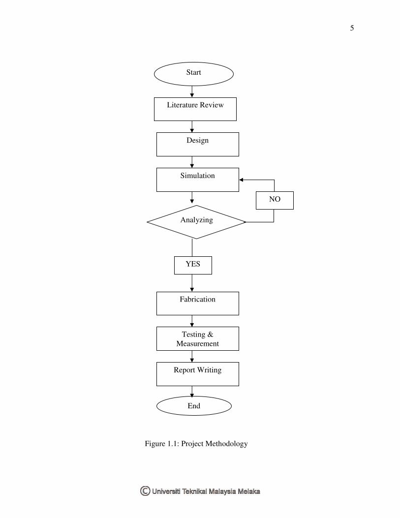
5
Figure 1.1: Project Methodology
Analyzing
NO
Literature Review
Start
YES
End
Design
Simulation
Report Writing
Testing &
Measurement
Fabrication

CHAPTER II
LITERATURE REVIEW
2.1 Antennas Concept
An antenna is defined by Webster’s Dictionary as “a usually metallic device (as a
rod or wire) for radiating or receiving radio waves.” The IEEE Standard Definitions of
Terms for Antennas (IEEE Std 145-1983) defines the antenna or aerial as a means for
radiating or receiving radio waves [8]. The purpose of and antenna is to transmit or
receive radio frequency energy. The function of an antenna when used at a transmitter is
to convert the radiated wave into useful radio frequency energy for the receiver [3].
In other words the antenna is the transitional structures between free-space and
guiding device, as shown in Figure the guiding device or transmission line may take the
form of a coaxial lie or a waveguide and it is used to transport electromagnetic energy
from transmitting source to the antenna or from the antenna to the receiver. In the
previous cases, we have a transmitting antenna and in the latter a receiving antenna.
In addition to receiving or transmitting energy, an antenna in an advanced
wireless system usually required to optimize or accentuate the radiation energy in some
directions and suppress it in others. Hence, the antenna must also serve as a directional