lm4923 1.1 watt fully differential audio power amplifier ... file1.1 watt fully differential audio...
TRANSCRIPT
LM4923
LM4923 1.1 Watt Fully Differential Audio Power Amplifier With Shutdown
Select
Literature Number: SNAS211D
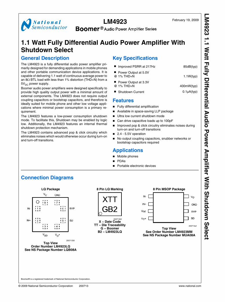
LM4923 February 19, 2009
1.1 Watt Fully Differential Audio Power Amplifier WithShutdown SelectGeneral DescriptionThe LM4923 is a fully differential audio power amplifier pri-marily designed for demanding applications in mobile phonesand other portable communication device applications. It iscapable of delivering 1.1 watt of continuous average power toan 8Ω BTL load with less than 1% distortion (THD+N) from a5VDC power supply.
Boomer audio power amplifiers were designed specifically toprovide high quality output power with a minimal amount ofexternal components. The LM4923 does not require outputcoupling capacitors or bootstrap capacitors, and therefore isideally suited for mobile phone and other low voltage appli-cations where minimal power consumption is a primary re-quirement.
The LM4923 features a low-power consumption shutdownmode. To facilitate this, Shutdown may be enabled by logiclow. Additionally, the LM4923 features an internal thermalshutdown protection mechanism.
The LM4923 contains advanced pop & click circuitry whicheliminates noises which would otherwise occur during turn-onand turn-off transitions.
Key Specifications
Improved PSRR at 217Hz 85dB(typ)
Power Output at 5.0V@ 1% THD+N 1.1W(typ)
Power Output at 3.3V@ 1% THD+N 400mW(typ)
Shutdown Current 0.1µA(typ)
Features Fully differential amplification
Available in space-saving LLP package
Ultra low current shutdown mode
Can drive capacitive loads up to 100pF
Improved pop & click circuitry eliminates noises duringturn-on and turn-off transitions
2.4 - 5.5V operation
No output coupling capacitors, snubber networks orbootstrap capacitors required
Applications Mobile phones
PDAs
Portable electronic devices
Connection Diagrams
LQ Package
20071330
Top ViewOrder Number LM4923LQ
See NS Package Number LQB08A
8 Pin LQ Marking
20071302
X − Date CodeTT − Die Traceability
G − BoomerB2 − LM4923LQ
8 Pin MSOP Package
200713a1
Top ViewSee Order Number LM4923MM
See NS Package Number MUA08A
Boomer® is a registered trademark of National Semiconductor Corporation.
© 2009 National Semiconductor Corporation 200713 www.national.com
LM
4923 1
.1 W
att F
ully
Diffe
ren
tial A
ud
io P
ow
er A
mp
lifier W
ith S
hu
tdo
wn
Sele
ct
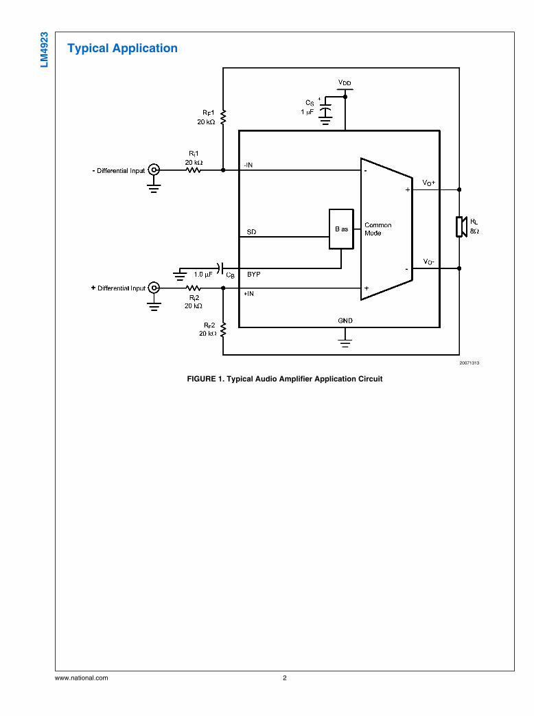
Typical Application
20071313
FIGURE 1. Typical Audio Amplifier Application Circuit
www.national.com 2
LM
4923
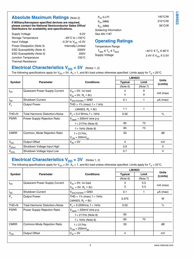
Absolute Maximum Ratings (Note 2)
If Military/Aerospace specified devices are required,please contact the National Semiconductor Sales Office/Distributors for availability and specifications.
Supply Voltage 6.0V
Storage Temperature −65°C to +150°C
Input Voltage −0.3V to VDD +0.3V
Power Dissipation (Note 3) Internally Limited
ESD Susceptibility (Note 4) 2000V
ESD Susceptibility (Note 5) 200V
Junction Temperature 150°C
Thermal Resistance
θJA (LLP) 140°C/W
θJA (MM) 210°C/W
θJC (MM) 56°C/W
Soldering Information
See AN-1187
Operating RatingsTemperature Range
TMIN ≤ TA ≤ TMAX −40°C ≤ TA ≤ 85°C
Supply Voltage 2.4V ≤ VDD ≤ 5.5V
Electrical Characteristics VDD = 5V (Notes 1, 2)
The following specifications apply for VDD = 5V, AV = 1, and 8Ω load unless otherwise specified. Limits apply for TA = 25°C.
Symbol Parameter Conditions
LM4923Units
(Limits)Typical Limit
(Note 6) (Note 7)
IDD Quiescent Power Supply Current VIN = 0V, no load
VIN = 0V, RL = 8Ω4
4
9
9mA (max)
ISD Shutdown Current VSHUTDOWN = GND 0.1 1 µA (max)
Po Output Power THD = 1% (max); f = 1 kHz
LM4923, RL = 8Ω 1.1 1
THD+N Total Harmonic Distortion+Noise Po = 0.4 Wrms; f = 1kHz 0.02 %
PSRR Power Supply Rejection Ratio Vripple = 200mV sine p-p
f = 217Hz (Note 8) 85 73
f = 1kHz (Note 8) 85 73
CMRR Common_Mode Rejection Ratio f = 217Hz,
VCM = 200mVpp
50 dB
VOS Output Offset VIN = 0V 4 mV
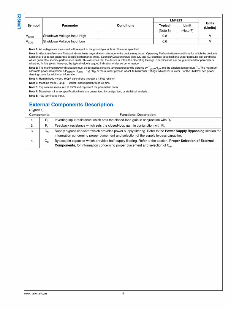
VSDIH Shutdown Voltage Input High 0.9 V
VSDIL Shutdown Voltage Input Low 0.7 V
Electrical Characteristics VDD = 3V (Notes 1, 2)
The following specifications apply for VDD = 3V, AV = 1, and 8Ω load unless otherwise specified. Limits apply for TA = 25°C.
Symbol Parameter Conditions
LM4923Units
(Limits)Typical Limit
(Note 6) (Note 7)
IDD Quiescent Power Supply Current VIN = 0V, no load
VIN = 0V, RL = 8Ω3
3
5.5
5.5mA (max)
ISD Shutdown Current VSHUTDOWN = GND 0.1 1 µA (max)
Po Output Power THD = 1% (max); f = 1kHz
LM4923, RL = 8Ω 0.375
W
THD+N Total Harmonic Distortion+Noise Po = 0.25Wrms; f = 1kHz 0.02 %
PSRR Power Supply Rejection Ratio Vripple = 200mV sine p-p
f = 217Hz (Note 8) 85
f = 1kHz (Note 8) 85 73
CMRR Common-Mode Rejection Ratio f = 217Hz
VCM = 200mVpp
50 dB
VOS Output Offset VIN = 0V 4 mV
3 www.national.com
LM
4923
Symbol Parameter Conditions
LM4923Units
(Limits)Typical Limit
(Note 6) (Note 7)
VSDIH Shutdown Voltage Input High 0.8 V
VSDIL Shutdown Voltage Input Low 0.6 V
Note 1: All voltages are measured with respect to the ground pin, unless otherwise specified.
Note 2: Absolute Maximum Ratings indicate limits beyond which damage to the device may occur. Operating Ratings indicate conditions for which the device isfunctional, but do not guarantee specific performance limits. Electrical Characteristics state DC and AC electrical specifications under particular test conditionswhich guarantee specific performance limits. This assumes that the device is within the Operating Ratings. Specifications are not guaranteed for parameterswhere no limit is given, however, the typical value is a good indication of device performance.
Note 3: The maximum power dissipation must be derated at elevated temperatures and is dictated by TJMAX, θJA, and the ambient temperature TA. The maximumallowable power dissipation is PDMAX = (TJMAX – TA) / θJA or the number given in Absolute Maximum Ratings, whichever is lower. For the LM4923, see powerderating curve for additional information.
Note 4: Human body model, 100pF discharged through a 1.5kΩ resistor.
Note 5: Machine Model, 220pF – 240pF discharged through all pins.
Note 6: Typicals are measured at 25°C and represent the parametric norm.
Note 7: Datasheet min/max specification limits are guaranteed by design, test, or statistical analysis.
Note 8: 10Ω terminated input.
External Components Description(Figure 1)
Components Functional Description
1. Ri Inverting input resistance which sets the closed-loop gain in conjunction with Rf.
2. Rf Feedback resistance which sets the closed-loop gain in conjunction with Ri.
3. CS Supply bypass capacitor which provides power supply filtering. Refer to the Power Supply Bypassing section for
information concerning proper placement and selection of the supply bypass capacitor.
4. CB Bypass pin capacitor which provides half-supply filtering. Refer to the section, Proper Selection of External
Components, for information concerning proper placement and selection of CB.
www.national.com 4
LM
4923
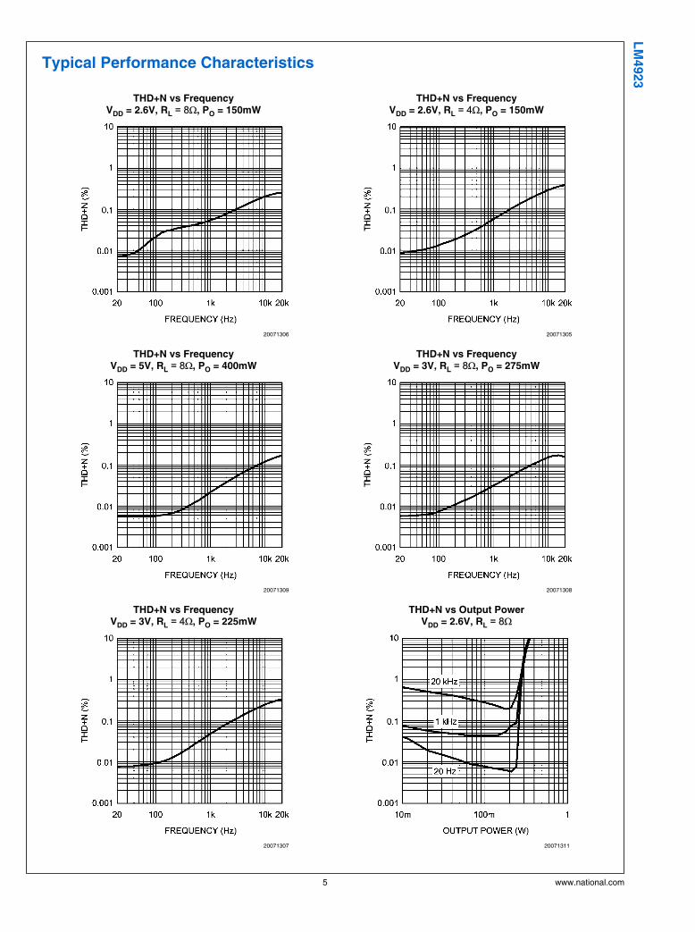
Typical Performance Characteristics
THD+N vs FrequencyVDD = 2.6V, RL = 8Ω, PO = 150mW
20071306
THD+N vs FrequencyVDD = 2.6V, RL = 4Ω, PO = 150mW
20071305
THD+N vs FrequencyVDD = 5V, RL = 8Ω, PO = 400mW
20071309
THD+N vs FrequencyVDD = 3V, RL = 8Ω, PO = 275mW
20071308
THD+N vs FrequencyVDD = 3V, RL = 4Ω, PO = 225mW
20071307
THD+N vs Output PowerVDD = 2.6V, RL = 8Ω
20071311
5 www.national.com
LM
4923
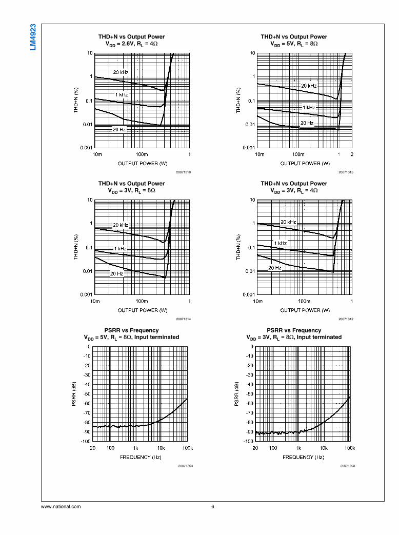
THD+N vs Output PowerVDD = 2.6V, RL = 4Ω
20071310
THD+N vs Output PowerVDD = 5V, RL = 8Ω
20071315
THD+N vs Output PowerVDD = 3V, RL = 8Ω
20071314
THD+N vs Output PowerVDD = 3V, RL = 4Ω
20071312
PSRR vs FrequencyVDD = 5V, RL = 8Ω, Input terminated
20071304
PSRR vs FrequencyVDD = 3V, RL = 8Ω, Input terminated
20071303
www.national.com 6
LM
4923
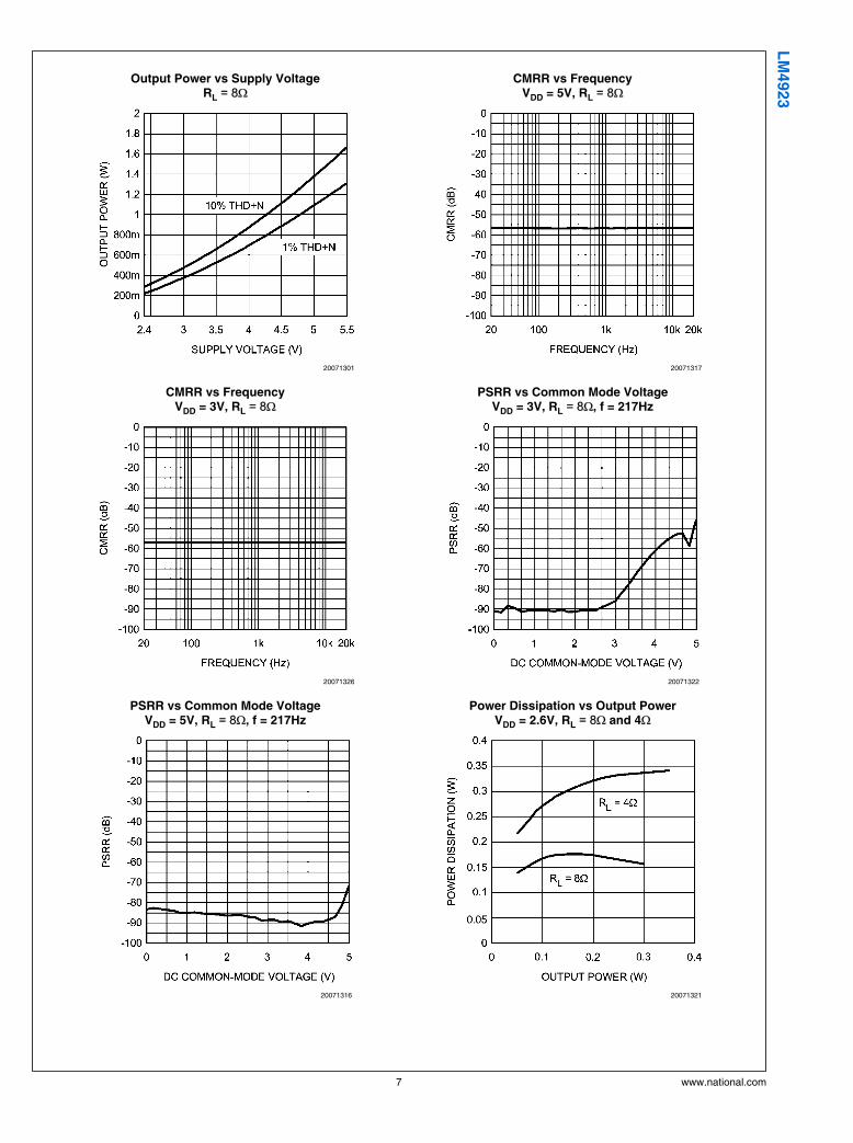
Output Power vs Supply VoltageRL = 8Ω
20071301
CMRR vs FrequencyVDD = 5V, RL = 8Ω
20071317
CMRR vs FrequencyVDD = 3V, RL = 8Ω
20071326
PSRR vs Common Mode VoltageVDD = 3V, RL = 8Ω, f = 217Hz
20071322
PSRR vs Common Mode VoltageVDD = 5V, RL = 8Ω, f = 217Hz
20071316
Power Dissipation vs Output PowerVDD = 2.6V, RL = 8Ω and 4Ω
20071321
7 www.national.com
LM
4923
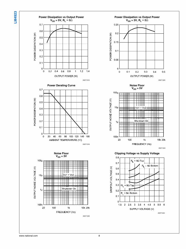
Power Dissipation vs Output PowerVDD = 5V, RL = 8Ω
20071319
Power Dissipation vs Output PowerVDD = 3V, RL = 8Ω
20071325
Power Derating Curve
20071318
Noise FloorVDD = 5V
20071324
Noise FloorVDD = 3V
20071320
Clipping Voltage vs Supply Voltage
20071323
www.national.com 8
LM
4923
Output Power vs Load Resistance
20071327
Supply Current Shutdown Voltage
20071328
Application Information
DIFFERENTIAL AMPLIFIER EXPLANATION
The LM4923 is a fully differential audio amplifier that featuresdifferential input and output stages. Internally this is accom-plished by two circuits: a differential amplifier and a commonmode feedback amplifier that adjusts the output voltages sothat the average value remains VDD / 2. When setting the dif-ferential gain, the amplifier can be considered to have"halves". Each half uses an input and feedback resistor (Ri1and RF1) to set its respective closed-loop gain (see Figure 1).With Ri1 = Ri2 and RF1 = RF2, the gain is set at -RF / Ri for eachhalf. This results in a differential gain of
AVD = -RF/Ri (1)
It is extremely important to match the input resistors to eachother, as well as the feedback resistors to each other for bestamplifier performance. See the Proper Selection of Exter-nal Components section for more information. A differentialamplifier works in a manner where the difference between thetwo input signals is amplified. In most applications, this wouldrequire input signals that are 180° out of phase with each oth-er. The LM4923 can be used, however, as a single endedinput amplifier while still retaining its fully differential benefits.In fact, completely unrelated signals may be placed on theinput pins. The LM4923 simply amplifies the difference be-tween them.
All of these applications provide what is known as a "bridgedmode" output (bridge-tied-load, BTL). This results in outputsignals at Vo1 and Vo2 that are 180° out of phase with respectto each other. Bridged mode operation is different from thesingle-ended amplifier configuration that connects the loadbetween the amplifier output and ground. A bridged amplifierdesign has distinct advantages over the single-ended config-uration: it provides differential drive to the load, thus doublingmaximum possible output swing for a specific supply voltage.Four times the output power is possible compared with a sin-gle-ended amplifier under the same conditions. This increasein attainable output power assumes that the amplifier is notcurrent limited or clipped. In order to choose an amplifier'sclosed-loop gain without causing excess clipping, please re-fer to the Audio Power Amplifier Design section.
A bridged configuration, such as the one used in the LM4923,also creates a second advantage over single-ended ampli-
fiers. Since the differential outputs, Vo1 and Vo2, are biased athalf-supply, no net DC voltage exists across the load. Thisassumes that the input resistor pair and the feedback resistorpair are properly matched (see Proper Selection of ExternalComponents). BTL configuration eliminates the output cou-pling capacitor required in single-supply, single-ended ampli-fier configurations. If an output coupling capacitor is not usedin a single-ended output configuration, the half-supply biasacross the load would result in both increased internal ICpower dissipation as well as permanent loudspeaker dam-age. Further advantages of bridged mode operation specificto fully differential amplifiers like the LM4923 include in-creased power supply rejection ratio, common-mode noisereduction, and click and pop reduction.
EXPOSED-DAP PACKAGE PCB MOUNTINGCONSIDERATIONS
The LM4923's exposed-DAP (die attach paddle) package(LLP) provide a low thermal resistance between the die andthe PCB to which the part is mounted and soldered. This al-lows rapid heat transfer from the die to the surrounding PCBcopper traces, ground plane and, finally, surrounding air. Fail-ing to optimize thermal design may compromise the LM4923'shigh power performance and activate unwanted, though nec-essary, thermal shutdown protection. The LLP package musthave its DAP soldered to a copper pad on the PCB. The DAP'sPCB copper pad is connected to a large plane of continuousunbroken copper. This plane forms a thermal mass and heatsink and radiation area. Place the heat sink area on eitheroutside plane in the case of a two-sided PCB, or on an innerlayer of a board with more than two layers. Connect the DAPcopper pad to the inner layer or backside copper heat sinkarea with a thermal via. The via diameter should be 0.012in -0.013in. Ensure efficient thermal conductivity by plating-through and solder-filling the vias.
Best thermal performance is achieved with the largest prac-tical copper heat sink area. In all circumstances and condi-tions, the junction temperature must be held below 150°C toprevent activating the LM4923's thermal shutdown protection.The LM4923's power de-rating curve in the Typical Perfor-mance Characteristics shows the maximum power dissipa-tion versus temperature. Example PCB layouts are shown inthe Demonstration Board Layout section. Further detailedand specific information concerning PCB layout, fabrication,and mounting an LLP package is available from National
9 www.national.com
LM
4923
Semiconductor's package Engineering Group under applica-tion note AN1187.
PCB LAYOUT AND SUPPLY REGULATIONCONSIDERATIONS FOR DRIVING 4Ω LOADS
Power dissipated by a load is a function of the voltage swingacross the load and the load's impedance. As load impedancedecreases, load dissipation becomes increasingly dependenton the interconnect (PCB trace and wire) resistance betweenthe amplifier output pins and the load's connections. Residualtrace resistance causes a voltage drop, which results in powerdissipated in the trace and not in the load as desired. Thisproblem of decreased load dissipation is exacerbated as loadimpedance decreases. Therefore, to maintain the highestload dissipation and widest output voltage swing, PCB tracesthat connect the output pins to a load must be as wide aspossible.
Poor power supply regulation adversely affects maximumoutput power. A poorly regulated supply's output voltage de-creases with increasing load current. Reduced supply voltagecauses decreased headroom, output signal clipping, and re-duced output power. Even with tightly regulated supplies,trace resistance creates the same effects as poor supply reg-ulation. Therefore, making the power supply traces as wideas possible helps maintain full output voltage swing.
POWER DISSIPATION
Power dissipation is a major concern when designing a suc-cessful amplifer, whether the amplifier is bridged or single-ended. Equation 2 states the maximum power dissipationpoint for a single-ended amplifier operating at a given supplyvoltage and driving a specified output load.
PDMAX = (VDD)2 / (2π2RL) Single-Ended (2)
However, a direct consequence of the increased power de-livered to the load by a bridge amplifier is an increase ininternal power dissipation versus a single-ended amplifier op-erating at the same conditions.
PDMAX = 4 * (VDD)2 / (2π2RL) Bridge Mode (3)
Since the LM4923 has bridged outputs, the maximum internalpower dissipation is 4 times that of a single-ended amplifier.Even with this substantial increase in power dissipation, theLM4923 does not require additional heatsinking under mostoperating conditions and output loading. From Equation 3,assuming a 5V power supply and an 8Ω load, the maximumpower dissipation point is 625mW. The maximum power dis-sipation point obtained from Equation 3 must not be greaterthan the power dissipation results from Equation 4:
PDMAX = (TJMAX - TA) / θJA (4)
The LM4923's θJA in an LQB08A package is 140°C/W. De-pending on the ambient temperature, TA, of the system sur-roundings, Equation 4 can be used to find the maximuminternal power dissipation supported by the IC packaging. Ifthe result of Equation 3 is greater than that of Equation 4, theneither the supply voltage must be decreased, the loadimpedance increased, the ambient temperature reduced, orthe θJA reduced with heatsinking. In many cases, larger tracesnear the output, VDD, and GND pins can be used to lower theθJA. The larger areas of copper provide a form of heatsinking
allowing higher power dissipation. For the typical applicationof a 5V power supply, with an 8Ω load, the maximum ambienttemperature possible without violating the maximum junctiontemperature is approximately 62°C provided that device op-eration is around the maximum power dissipation point. Re-call that internal power dissipation is a function of outputpower. If typical operation is not around the maximum powerdissipation point, the LM4923 can operate at higher ambienttemperatures. Refer to the Typical Performance Charac-teristics curves for power dissipation information.
POWER SUPPLY BYPASSING
As with any power amplifier, proper supply bypassing is crit-ical for low noise performance and high power supply rejec-tion ratio (PSRR). The capacitor location on both the bypassand power supply pins should be as close to the device aspossible. A larger half-supply bypass capacitor improvesPSRR because it increases half-supply stability. Typical ap-plications employ a 5V regulator with 10µF and 0.1µF bypasscapacitors that increase supply stability. This, however, doesnot eliminate the need for bypassing the supply nodes of theLM4923. The LM4923 will operate without the bypass capac-itor CB, although the PSRR may decrease. A 1µF capacitor isrecommended for CB. This value maximizes PSRR perfor-mance. Lesser values may be used, but PSRR decreases atfrequencies below 1kHz. The issue of CB selection is thusdependant upon desired PSRR and click and pop perfor-mance as explained in the section Proper Selection of Ex-ternal Components.
SHUTDOWN FUNCTION
In order to reduce power consumption while not in use, theLM4923 contains shutdown circuitry that is used to turn off theamplifier's bias circuitry. The device may then be placed intoshutdown mode by toggling the Shutdown Select pin to logiclow. The trigger point for shutdown is shown as a typical valuein the Supply Current vs Shutdown Voltage graphs in theTypical Performance Characteristics section. It is best toswitch between ground and supply for maximum perfor-mance. While the device may be disabled with shutdownvoltages in between ground and supply, the idle current maybe greater than the typical value of 0.1µA. In either case, theshutdown pin should be tied to a definite voltage to avoid un-wanted state changes.
In many applications, a microcontroller or microprocessoroutput is used to control the shutdown circuitry, which pro-vides a quick, smooth transition to shutdown. Another solutionis to use a single-throw switch in conjunction with an externalpull-up resistor. This scheme guarantees that the shutdownpin will not float, thus preventing unwanted state changes.
PROPER SELECTION OF EXTERNAL COMPONENTS
Proper selection of external components in applications usingintegrated power amplifiers is critical when optimizing deviceand system performance. Although the LM4923 is tolerant toa variety of external component combinations, considerationof component values must be made when maximizing overallsystem quality.
The LM4923 is unity-gain stable, giving the designer maxi-mum system flexibility. The LM4923 should be used in lowclosed-loop gain configurations to minimize THD+N valuesand maximize signal to noise ratio. Low gain configurationsrequire large input signals to obtain a given output power. In-put signals equal to or greater than 1Vrms are available fromsources such as audio codecs. Please refer to the AudioPower Amplifier Design section for a more complete expla-
www.national.com 10
LM
4923
nation of proper gain selection. When used in its typicalapplication as a fully differential power amplifier the LM4923does not require input coupling capacitors for input sourceswith DC common-mode voltages of less than VDD. Exact al-lowable input common-mode voltage levels are actually afunction of VDD, Ri, and Rf and may be determined by Equa-tion 5:
VCMi < (VDD-1.2)*((Rf+(Ri)/(Rf)-VDD*(Ri / 2Rf) (5)
-RF / RI = AVD (6)
Special care must be taken to match the values of the feed-back resistors (RF1 and RF2) to each other as well as matchingthe input resistors (Ri1 and Ri2) to each other (see Figure 1)more in front. Because of the balanced nature of differentialamplifiers, resistor matching differences can result in net DCcurrents across the load. This DC current can increase powerconsumption, internal IC power dissipation, reduce PSRR,and possibly damaging the loudspeaker. The chart belowdemonstrates this problem by showing the effects of differingvalues between the feedback resistors while assuming thatthe input resistors are perfectly matched. The results belowapply to the application circuit shown in Figure 1, and as-sumes that VDD = 5V, RL = 8Ω, and the system has DCcoupled inputs tied to ground.
Tolerance RF1 RF2 V02 - V01 ILOAD
20% 0.8R 1.2R -0.500V 62.5mA
10% 0.9R 1.1R -0.250V 31.25mA
5% 0.95R 1.05R -0.125V 15.63mA
1% 0.99R 1.01R -0.025V 3.125mA
0% R R 0 0
Similar results would occur if the input resistors were notcarefully matched. Adding input coupling capacitors in be-tween the signal source and the input resistors will eliminatethis problem, however, to achieve best performance with min-imum component count it is highly recommended that boththe feedback and input resistors matched to 1% tolerance orbetter.
AUDIO POWER AMPLIFIER DESIGN
Design a 1W/8Ω Audio Amplifier
Given:
Power Output 1Wrms
Load Impedance 8Ω Input Level 1Vrms
Input Impedance 20kΩ Bandwidth 100Hz–20kHz ± 0.25dB
A designer must first determine the minimum supply rail toobtain the specified output power. The supply rail can easilybe found by extrapolating from the Output Power vs SupplyVoltage graphs in the Typical Performance Characteris-tics section. A second way to determine the minimum supplyrail is to calculate the required VOPEAK using Equation 7 andadd the dropout voltages. Using this method, the minimumsupply voltage is (Vopeak + (VDO TOP + (VDO BOT )), whereVDO BOT and VDO TOP are extrapolated from the Dropout Volt-age vs Supply Voltage curve in the Typical PerformanceCharacteristics section.
(7)
Using the Output Power vs Supply Voltage graph for an 8Ωload, the minimum supply rail just about 5V. Extra supply volt-age creates headroom that allows the LM4923 to reproducepeaks in excess of 1W without producing audible distortion.At this time, the designer must make sure that the power sup-ply choice along with the output impedance does not violatethe conditions explained in the Power Dissipation section.Once the power dissipation equations have been addressed,the required differential gain can be determined from Equa-tion 8.
(8)
Rf / Ri = AVD
From Equation 7, the minimum AVD is 2.83. Since the desiredinput impedance was 20kΩ, a ratio of 2.83:1 of Rf to Ri resultsin an allocation of Ri = 20kΩ for both input resistors and Rf =60kΩ for both feedback resistors. The final design step is toaddress the bandwidth requirement which must be stated asa single -3dB frequency point. Five times away from a -3dBpoint is 0.17dB down from passband response which is betterthan the required ±0.25dB specified.
fH = 20kHz * 5 = 100kHz
The high frequency pole is determined by the product of thedesired frequency pole, fH , and the differential gain, AVD .With a AVD = 2.83 and fH = 100kHz, the resulting GBWP =150kHz which is much smaller than the LM4923 GBWP of10MHz. This figure displays that if a designer has a need todesign an amplifier with a higher differential gain, the LM4923can still be used without running into bandwidth limitations.
11 www.national.com
LM
4923
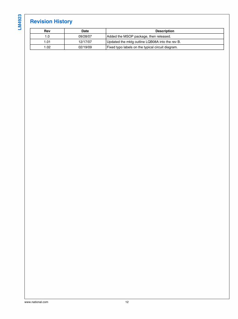
Revision History
Rev Date Description
1.0 09/28/07 Added the MSOP package, then released.
1.01 12/17/07 Updated the mktg outline LQB08A into the rev B.
1.02 02/19/09 Fixed typo labels on the typical circuit diagram.
www.national.com 12
LM
4923
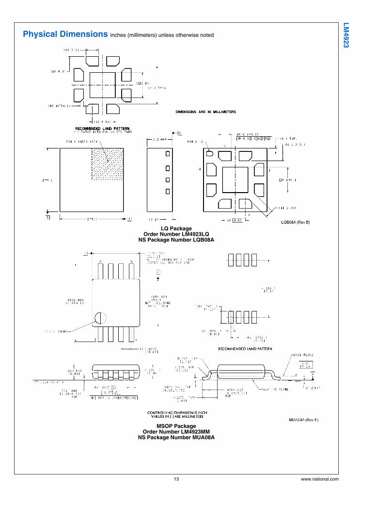
Physical Dimensions inches (millimeters) unless otherwise noted
LQ PackageOrder Number LM4923LQ
NS Package Number LQB08A
MSOP PackageOrder Number LM4923MM
NS Package Number MUA08A
13 www.national.com
LM
4923
NotesL
M4923 1
.1 W
att
Fu
lly D
iffe
ren
tial A
ud
io P
ow
er
Am
plifi
er
Wit
h S
hu
tdo
wn
Sele
ct
For more National Semiconductor product information and proven design tools, visit the following Web sites at:
Products Design Support
Amplifiers www.national.com/amplifiers WEBENCH® Tools www.national.com/webench
Audio www.national.com/audio App Notes www.national.com/appnotes
Clock and Timing www.national.com/timing Reference Designs www.national.com/refdesigns
Data Converters www.national.com/adc Samples www.national.com/samples
Interface www.national.com/interface Eval Boards www.national.com/evalboards
LVDS www.national.com/lvds Packaging www.national.com/packaging
Power Management www.national.com/power Green Compliance www.national.com/quality/green
Switching Regulators www.national.com/switchers Distributors www.national.com/contacts
LDOs www.national.com/ldo Quality and Reliability www.national.com/quality
LED Lighting www.national.com/led Feedback/Support www.national.com/feedback
Voltage Reference www.national.com/vref Design Made Easy www.national.com/easy
PowerWise® Solutions www.national.com/powerwise Solutions www.national.com/solutions
Serial Digital Interface (SDI) www.national.com/sdi Mil/Aero www.national.com/milaero
Temperature Sensors www.national.com/tempsensors SolarMagic™ www.national.com/solarmagic
Wireless (PLL/VCO) www.national.com/wireless Analog University® www.national.com/AU
THE CONTENTS OF THIS DOCUMENT ARE PROVIDED IN CONNECTION WITH NATIONAL SEMICONDUCTOR CORPORATION(“NATIONAL”) PRODUCTS. NATIONAL MAKES NO REPRESENTATIONS OR WARRANTIES WITH RESPECT TO THE ACCURACYOR COMPLETENESS OF THE CONTENTS OF THIS PUBLICATION AND RESERVES THE RIGHT TO MAKE CHANGES TOSPECIFICATIONS AND PRODUCT DESCRIPTIONS AT ANY TIME WITHOUT NOTICE. NO LICENSE, WHETHER EXPRESS,IMPLIED, ARISING BY ESTOPPEL OR OTHERWISE, TO ANY INTELLECTUAL PROPERTY RIGHTS IS GRANTED BY THISDOCUMENT.
TESTING AND OTHER QUALITY CONTROLS ARE USED TO THE EXTENT NATIONAL DEEMS NECESSARY TO SUPPORTNATIONAL’S PRODUCT WARRANTY. EXCEPT WHERE MANDATED BY GOVERNMENT REQUIREMENTS, TESTING OF ALLPARAMETERS OF EACH PRODUCT IS NOT NECESSARILY PERFORMED. NATIONAL ASSUMES NO LIABILITY FORAPPLICATIONS ASSISTANCE OR BUYER PRODUCT DESIGN. BUYERS ARE RESPONSIBLE FOR THEIR PRODUCTS ANDAPPLICATIONS USING NATIONAL COMPONENTS. PRIOR TO USING OR DISTRIBUTING ANY PRODUCTS THAT INCLUDENATIONAL COMPONENTS, BUYERS SHOULD PROVIDE ADEQUATE DESIGN, TESTING AND OPERATING SAFEGUARDS.
EXCEPT AS PROVIDED IN NATIONAL’S TERMS AND CONDITIONS OF SALE FOR SUCH PRODUCTS, NATIONAL ASSUMES NOLIABILITY WHATSOEVER, AND NATIONAL DISCLAIMS ANY EXPRESS OR IMPLIED WARRANTY RELATING TO THE SALEAND/OR USE OF NATIONAL PRODUCTS INCLUDING LIABILITY OR WARRANTIES RELATING TO FITNESS FOR A PARTICULARPURPOSE, MERCHANTABILITY, OR INFRINGEMENT OF ANY PATENT, COPYRIGHT OR OTHER INTELLECTUAL PROPERTYRIGHT.
LIFE SUPPORT POLICY
NATIONAL’S PRODUCTS ARE NOT AUTHORIZED FOR USE AS CRITICAL COMPONENTS IN LIFE SUPPORT DEVICES ORSYSTEMS WITHOUT THE EXPRESS PRIOR WRITTEN APPROVAL OF THE CHIEF EXECUTIVE OFFICER AND GENERALCOUNSEL OF NATIONAL SEMICONDUCTOR CORPORATION. As used herein:
Life support devices or systems are devices which (a) are intended for surgical implant into the body, or (b) support or sustain life andwhose failure to perform when properly used in accordance with instructions for use provided in the labeling can be reasonably expectedto result in a significant injury to the user. A critical component is any component in a life support device or system whose failure to performcan be reasonably expected to cause the failure of the life support device or system or to affect its safety or effectiveness.
National Semiconductor and the National Semiconductor logo are registered trademarks of National Semiconductor Corporation. All otherbrand or product names may be trademarks or registered trademarks of their respective holders.
Copyright© 2009 National Semiconductor Corporation
For the most current product information visit us at www.national.com
National SemiconductorAmericas TechnicalSupport CenterEmail: [email protected]: 1-800-272-9959
National Semiconductor EuropeTechnical Support CenterEmail: [email protected]
National Semiconductor AsiaPacific Technical Support CenterEmail: [email protected]
National Semiconductor JapanTechnical Support CenterEmail: [email protected]
www.national.com

IMPORTANT NOTICE
Texas Instruments Incorporated and its subsidiaries (TI) reserve the right to make corrections, modifications, enhancements, improvements,and other changes to its products and services at any time and to discontinue any product or service without notice. Customers shouldobtain the latest relevant information before placing orders and should verify that such information is current and complete. All products aresold subject to TI’s terms and conditions of sale supplied at the time of order acknowledgment.
TI warrants performance of its hardware products to the specifications applicable at the time of sale in accordance with TI’s standardwarranty. Testing and other quality control techniques are used to the extent TI deems necessary to support this warranty. Except wheremandated by government requirements, testing of all parameters of each product is not necessarily performed.
TI assumes no liability for applications assistance or customer product design. Customers are responsible for their products andapplications using TI components. To minimize the risks associated with customer products and applications, customers should provideadequate design and operating safeguards.
TI does not warrant or represent that any license, either express or implied, is granted under any TI patent right, copyright, mask work right,or other TI intellectual property right relating to any combination, machine, or process in which TI products or services are used. Informationpublished by TI regarding third-party products or services does not constitute a license from TI to use such products or services or awarranty or endorsement thereof. Use of such information may require a license from a third party under the patents or other intellectualproperty of the third party, or a license from TI under the patents or other intellectual property of TI.
Reproduction of TI information in TI data books or data sheets is permissible only if reproduction is without alteration and is accompaniedby all associated warranties, conditions, limitations, and notices. Reproduction of this information with alteration is an unfair and deceptivebusiness practice. TI is not responsible or liable for such altered documentation. Information of third parties may be subject to additionalrestrictions.
Resale of TI products or services with statements different from or beyond the parameters stated by TI for that product or service voids allexpress and any implied warranties for the associated TI product or service and is an unfair and deceptive business practice. TI is notresponsible or liable for any such statements.
TI products are not authorized for use in safety-critical applications (such as life support) where a failure of the TI product would reasonablybe expected to cause severe personal injury or death, unless officers of the parties have executed an agreement specifically governingsuch use. Buyers represent that they have all necessary expertise in the safety and regulatory ramifications of their applications, andacknowledge and agree that they are solely responsible for all legal, regulatory and safety-related requirements concerning their productsand any use of TI products in such safety-critical applications, notwithstanding any applications-related information or support that may beprovided by TI. Further, Buyers must fully indemnify TI and its representatives against any damages arising out of the use of TI products insuch safety-critical applications.
TI products are neither designed nor intended for use in military/aerospace applications or environments unless the TI products arespecifically designated by TI as military-grade or "enhanced plastic." Only products designated by TI as military-grade meet militaryspecifications. Buyers acknowledge and agree that any such use of TI products which TI has not designated as military-grade is solely atthe Buyer's risk, and that they are solely responsible for compliance with all legal and regulatory requirements in connection with such use.
TI products are neither designed nor intended for use in automotive applications or environments unless the specific TI products aredesignated by TI as compliant with ISO/TS 16949 requirements. Buyers acknowledge and agree that, if they use any non-designatedproducts in automotive applications, TI will not be responsible for any failure to meet such requirements.
Following are URLs where you can obtain information on other Texas Instruments products and application solutions:
Products Applications
Audio www.ti.com/audio Communications and Telecom www.ti.com/communications
Amplifiers amplifier.ti.com Computers and Peripherals www.ti.com/computers
Data Converters dataconverter.ti.com Consumer Electronics www.ti.com/consumer-apps
DLP® Products www.dlp.com Energy and Lighting www.ti.com/energy
DSP dsp.ti.com Industrial www.ti.com/industrial
Clocks and Timers www.ti.com/clocks Medical www.ti.com/medical
Interface interface.ti.com Security www.ti.com/security
Logic logic.ti.com Space, Avionics and Defense www.ti.com/space-avionics-defense
Power Mgmt power.ti.com Transportation and Automotive www.ti.com/automotive
Microcontrollers microcontroller.ti.com Video and Imaging www.ti.com/video
RFID www.ti-rfid.com
OMAP Mobile Processors www.ti.com/omap
Wireless Connectivity www.ti.com/wirelessconnectivity
TI E2E Community Home Page e2e.ti.com
Mailing Address: Texas Instruments, Post Office Box 655303, Dallas, Texas 75265Copyright © 2011, Texas Instruments Incorporated