list of experiments - studentsfocusstudentsfocus.com/notes/anna_university/eee/3sem... · list of...
TRANSCRIPT
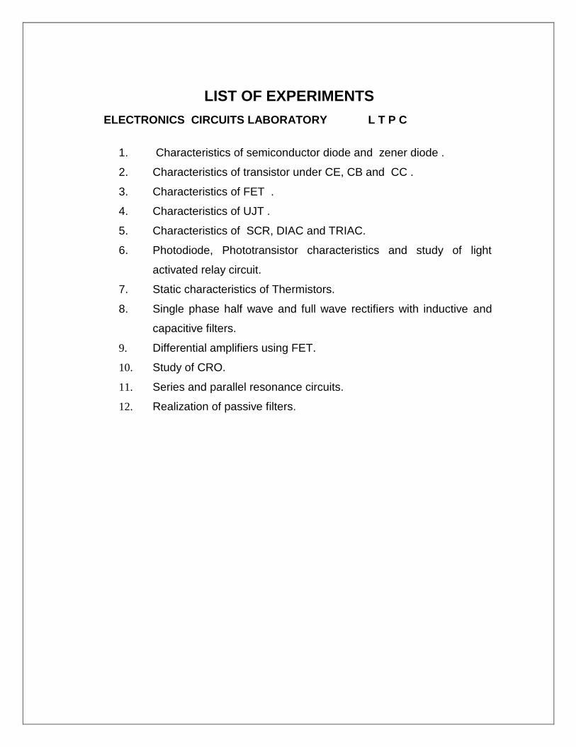
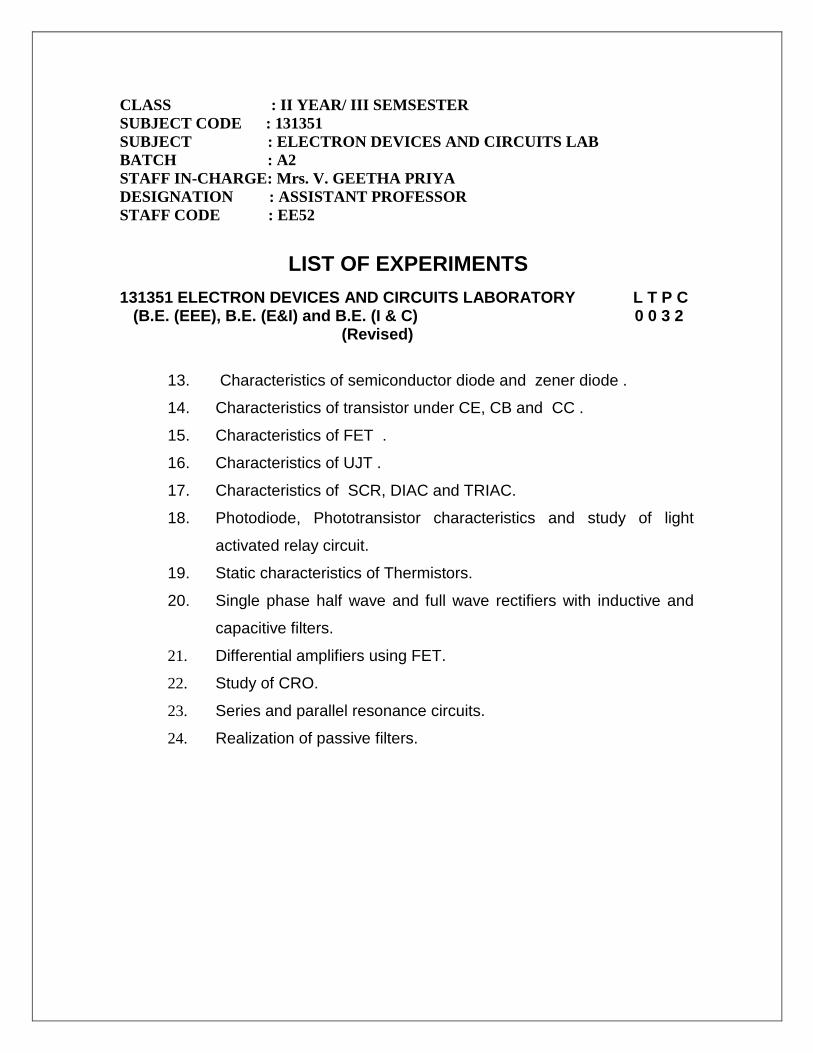
LIST OF EXPERIMENTS
ELECTRONICS CIRCUITS LABORATORY L T P C
1. Characteristics of semiconductor diode and zener diode .
2. Characteristics of transistor under CE, CB and CC .
3. Characteristics of FET .
4. Characteristics of UJT .
5. Characteristics of SCR, DIAC and TRIAC.
6. Photodiode, Phototransistor characteristics and study of light
activated relay circuit.
7. Static characteristics of Thermistors.
8. Single phase half wave and full wave rectifiers with inductive and
capacitive filters.
9. Differential amplifiers using FET.
10. Study of CRO.
11. Series and parallel resonance circuits.
12. Realization of passive filters.
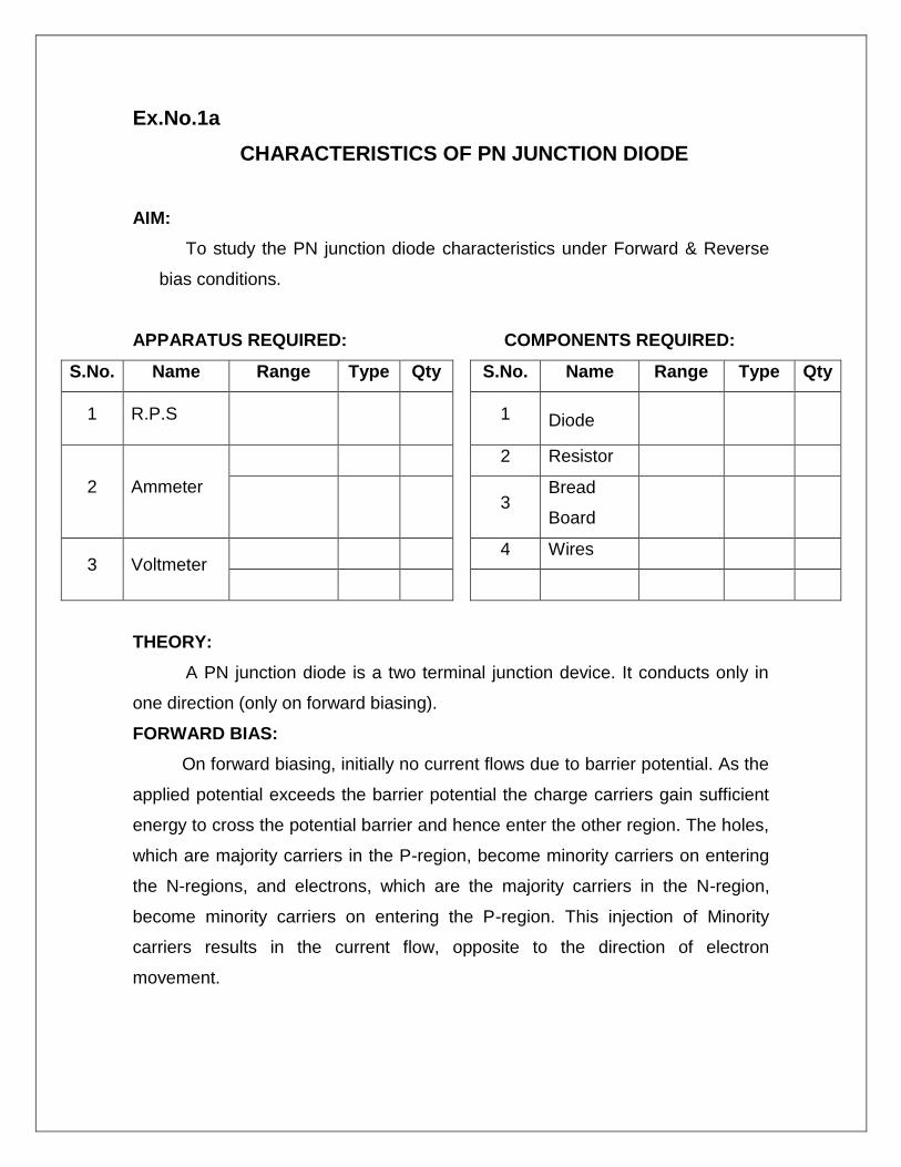
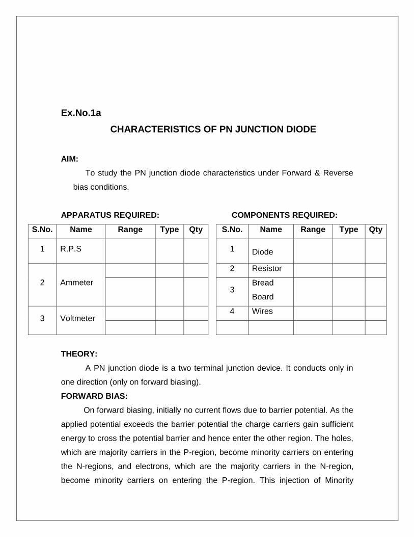
Ex.No.1a
CHARACTERISTICS OF PN JUNCTION DIODE
AIM:
To study the PN junction diode characteristics under Forward & Reverse
bias conditions.
APPARATUS REQUIRED: COMPONENTS REQUIRED:
S.No. Name Range Type Qty
S.No. Name Range Type Qty
1 R.P.S 1 Diode
2 Ammeter
2 Resistor
3 Bread
Board
3 Voltmeter 4 Wires
THEORY:
A PN junction diode is a two terminal junction device. It conducts only in
one direction (only on forward biasing).
FORWARD BIAS:
On forward biasing, initially no current flows due to barrier potential. As the
applied potential exceeds the barrier potential the charge carriers gain sufficient
energy to cross the potential barrier and hence enter the other region. The holes,
which are majority carriers in the P-region, become minority carriers on entering
the N-regions, and electrons, which are the majority carriers in the N-region,
become minority carriers on entering the P-region. This injection of Minority
carriers results in the current flow, opposite to the direction of electron
movement.
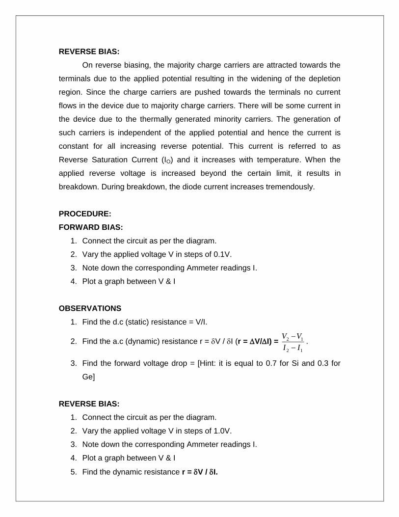
REVERSE BIAS:
On reverse biasing, the majority charge carriers are attracted towards the
terminals due to the applied potential resulting in the widening of the depletion
region. Since the charge carriers are pushed towards the terminals no current
flows in the device due to majority charge carriers. There will be some current in
the device due to the thermally generated minority carriers. The generation of
such carriers is independent of the applied potential and hence the current is
constant for all increasing reverse potential. This current is referred to as
Reverse Saturation Current (IO) and it increases with temperature. When the
applied reverse voltage is increased beyond the certain limit, it results in
breakdown. During breakdown, the diode current increases tremendously.
PROCEDURE:
FORWARD BIAS:
1. Connect the circuit as per the diagram.
2. Vary the applied voltage V in steps of 0.1V.
3. Note down the corresponding Ammeter readings I.
4. Plot a graph between V & I
OBSERVATIONS
1. Find the d.c (static) resistance = V/I.
2. Find the a.c (dynamic) resistance r = V / I (r = V/I) = 12
12
II
VV
.
3. Find the forward voltage drop = [Hint: it is equal to 0.7 for Si and 0.3 for
Ge]
REVERSE BIAS:
1. Connect the circuit as per the diagram.
2. Vary the applied voltage V in steps of 1.0V.
3. Note down the corresponding Ammeter readings I.
4. Plot a graph between V & I
5. Find the dynamic resistance r = V / I.

(0-100)mA, MC
+ -
+
+
-
+
(0-15)V, MC +
-
+
(0-10)V
RPS
(0-500)µA,MC
+ -
+
+
-
+
(0-30)V, MC +
-
+
(0-30)V
RPS
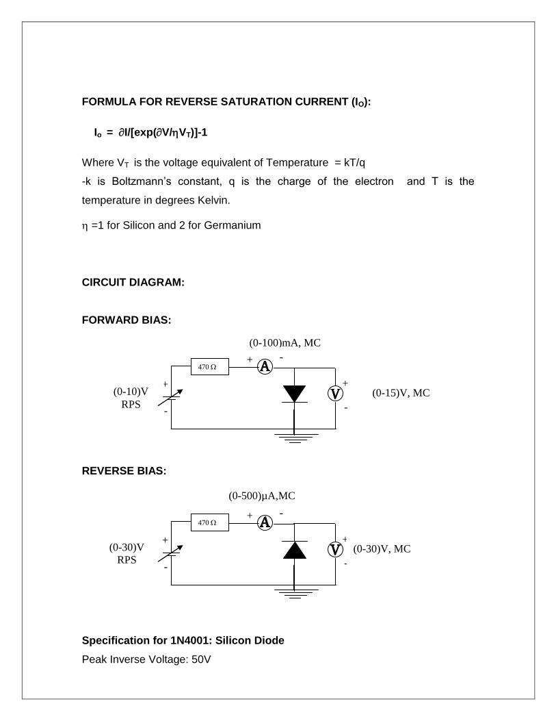
FORMULA FOR REVERSE SATURATION CURRENT (IO):
Io = I/[exp(V/VT)]-1
Where VT is the voltage equivalent of Temperature = kT/q
-k is Boltzmann’s constant, q is the charge of the electron and T is the
temperature in degrees Kelvin.
=1 for Silicon and 2 for Germanium
CIRCUIT DIAGRAM:
FORWARD BIAS:
REVERSE BIAS:
Specification for 1N4001: Silicon Diode
Peak Inverse Voltage: 50V
470 a
a
a
a
a
A
A
A
470 a
a
a
a
a
A
A
A

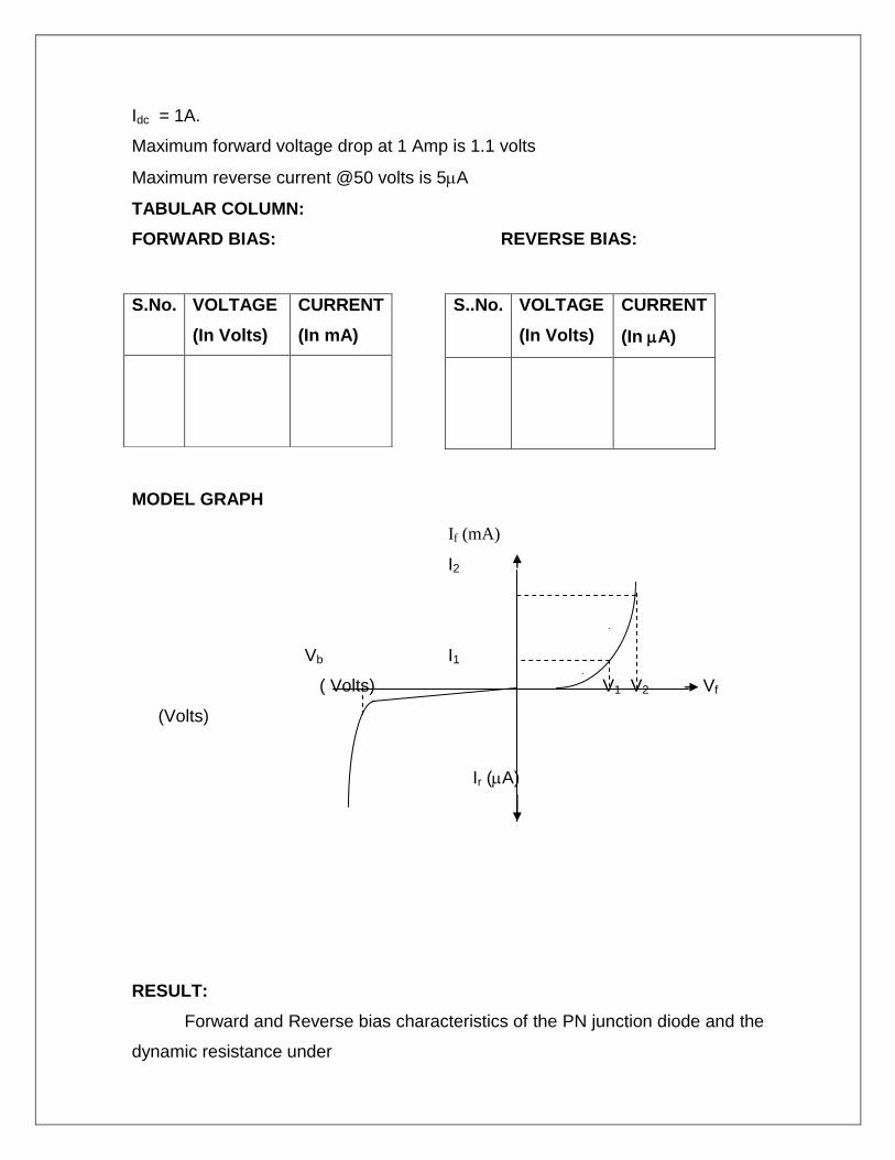
Idc = 1A.
Maximum forward voltage drop at 1 Amp is 1.1 volts
Maximum reverse current @50 volts is 5A
TABULAR COLUMN:
FORWARD BIAS: REVERSE BIAS:
MODEL GRAPH
If (mA)
I2
Vb I1
( Volts) V1 V2 Vf
(Volts)
Ir (A)
RESULT:
Forward and Reverse bias characteristics of the PN junction diode and the
dynamic resistance under
S.No. VOLTAGE
(In Volts)
CURRENT
(In mA)
S..No. VOLTAGE
(In Volts)
CURRENT
(In A)

i) Forward bias = ---------------------
ii) Reverse bias = ----------------------.
iii) Reverse Saturation Current = ----------------.

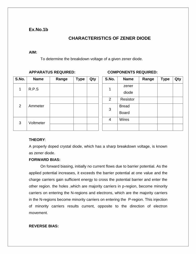
Ex.No.1b
CHARACTERISTICS OF ZENER DIODE
AIM:
To determine the breakdown voltage of a given zener diode.
APPARATUS REQUIRED: COMPONENTS REQUIRED:
S.No. Name Range Type Qty
S.No. Name Range Type Qty
1 R.P.S 1 zener
diode
2 Ammeter
2 Resistor
3 Bread
Board
3 Voltmeter 4 Wires
THEORY:
A properly doped crystal diode, which has a sharp breakdown voltage, is known
as zener diode.
FORWARD BIAS:
On forward biasing, initially no current flows due to barrier potential. As the
applied potential increases, it exceeds the barrier potential at one value and the
charge carriers gain sufficient energy to cross the potential barrier and enter the
other region. the holes ,which are majority carriers in p-region, become minority
carriers on entering the N-regions and electrons, which are the majority carriers
in the N-regions become minority carriers on entering the P-region. This injection
of minority carriers results current, opposite to the direction of electron
movement.
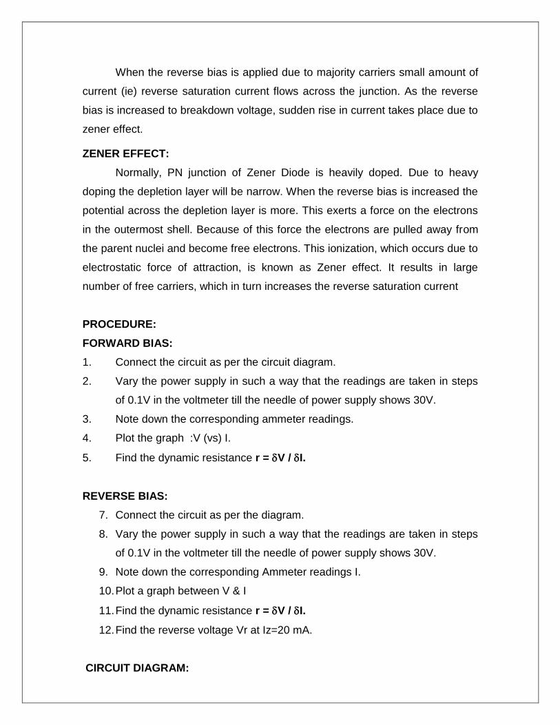
REVERSE BIAS:

When the reverse bias is applied due to majority carriers small amount of
current (ie) reverse saturation current flows across the junction. As the reverse
bias is increased to breakdown voltage, sudden rise in current takes place due to
zener effect.
ZENER EFFECT:
Normally, PN junction of Zener Diode is heavily doped. Due to heavy
doping the depletion layer will be narrow. When the reverse bias is increased the
potential across the depletion layer is more. This exerts a force on the electrons
in the outermost shell. Because of this force the electrons are pulled away from
the parent nuclei and become free electrons. This ionization, which occurs due to
electrostatic force of attraction, is known as Zener effect. It results in large
number of free carriers, which in turn increases the reverse saturation current
PROCEDURE:
FORWARD BIAS:
1. Connect the circuit as per the circuit diagram.
2. Vary the power supply in such a way that the readings are taken in steps
of 0.1V in the voltmeter till the needle of power supply shows 30V.
3. Note down the corresponding ammeter readings.
4. Plot the graph :V (vs) I.
5. Find the dynamic resistance r = V / I.
REVERSE BIAS:
1. Connect the circuit as per the diagram.
2. Vary the power supply in such a way that the readings are taken in steps
of 0.1V in the voltmeter till the needle of power supply shows 30V.
3. Note down the corresponding Ammeter readings I.
4. Plot a graph between V & I
5. Find the dynamic resistance r = V / I.
6. Find the reverse voltage Vr at Iz=20 mA.
CIRCUIT DIAGRAM:

(0-15) V
+ -
+
-
+
-
(0-10) V
(0-10) V, MC
+ -
+
-
+
-
(0-30) V
FORWARD BIAS:
REVERSE BIAS:
1K
a
a
a
a
a
A
A
A
a
a
a
a
a
A
A
A
470
aaaa
aAA
A
aaaa
aAA
A
a
a
a
a
a
A
A
A
(0-10)mA
1
K
a
a
a
a
a
A
A
A
a
a
a
a
a
A
A
A
1K
aaaa
aAA
A
aaaa
aAA
A
a
a
a
a
a
A
A
A
(0-500)μA, MC

ZENER DIODE:
If ( mA)
I2
VB I1
Vr V1 V2 Vf
(V) (V)
Ir (μA)
TABULAR COLUMN:
FORWARD BIAS: REVERSE BIAS:
RESULT:
Forward and Reverse bias characteristics of the zener diode was studied
and
Forward bias dynamic resistance = ---------------------
Reverse bias dynamic resistance = ----------------------
The reverse voltage at Iz =20 mA determined from the reverse
characteristics of the Zener diode is --------------------------.
S..No. VOLTAGE
(In Volts)
CURRENT
(In mA)
S.No. VOLTAGE
(In Volts)
CURRENT
(In A)

Ex. No. 2a
CHARACTERISTICS OF CE CONFIGURATION USING BJT
AIM:
To plot the transistor characteristics of CE configuration.
APPARATUS REQUIRED: COMPONENTS REQUIRED:
S.No. Name Range Type Qty
S.No. Name Range Type Qty
1 R.P.S 1 Transistor
2 Ammeter
2 Resistor
3 Bread
Board
3 Voltmeter 4 Wires
THEORY:
A BJT is a three terminal two – junction semiconductor device in which the
conduction is due to both the charge carrier. Hence it is a bipolar device and it
amplifier the sine waveform as they are transferred from input to output. BJT is
classified into two types – NPN or PNP. A NPN transistor consists of two N
types in between which a layer of P is sandwiched. The transistor consists of
three terminal emitter, collector and base. The emitter layer is the source of the
charge carriers and it is heartily doped with a moderate cross sectional area.
The collector collects the charge carries and hence moderate doping and large
cross sectional area. The base region acts a path for the movement of the
charge carriers. In order to reduce the recombination of holes and electrons the
base region is lightly doped and is of hollow cross sectional area. Normally the
transistor operates with the EB junction forward biased.
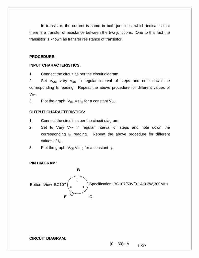
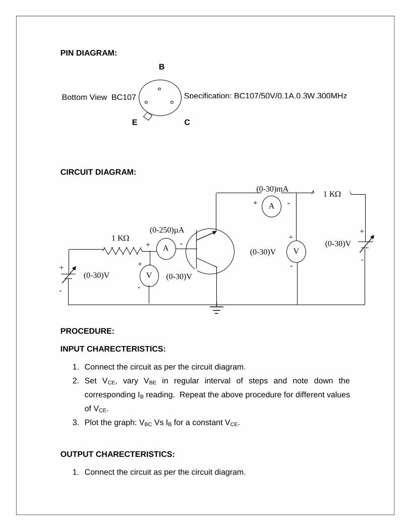
Bottom View BC107 Specification: BC107/50V/0.1A,0.3W,300MHz
(0 – 30)mA 1 K
In transistor, the current is same in both junctions, which indicates that
there is a transfer of resistance between the two junctions. One to this fact the
transistor is known as transfer resistance of transistor.
PROCEDURE:
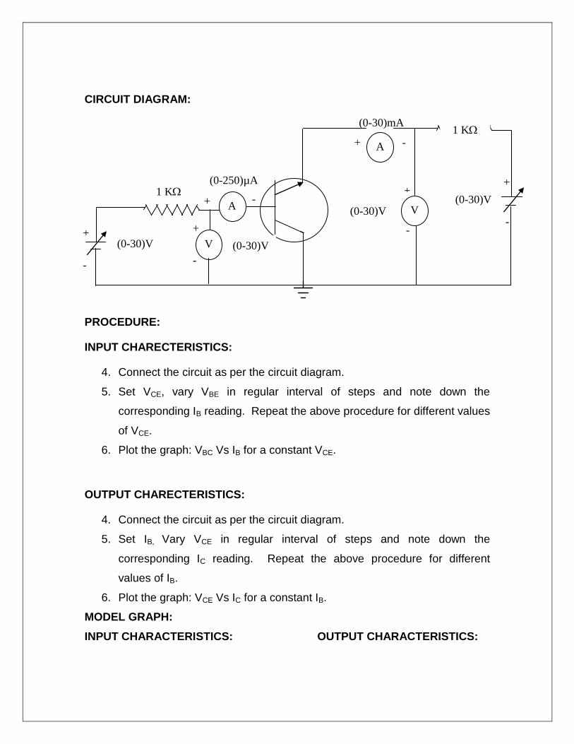
INPUT CHARACTERISTICS:
1. Connect the circuit as per the circuit diagram.
2. Set VCE, vary VBE in regular interval of steps and note down the
corresponding IB reading. Repeat the above procedure for different values of
VCE.
3. Plot the graph: VBE Vs IB for a constant VCE.
OUTPUT CHARACTERISTICS:
1. Connect the circuit as per the circuit diagram.
2. Set IB, Vary VCE in regular interval of steps and note down the
corresponding IC reading. Repeat the above procedure for different
values of IB.
3. Plot the graph: VCE Vs IC for a constant IB.
PIN DIAGRAM:
B
E C
CIRCUIT DIAGRAM:

(0 – 250) A
10 K
- +
BC107
10 KΩ
+
-
+
+
-
+
(0-30)V
+
-
+
+
-
+
+ -
+
(0-30)V
(0-30)V
(0-1)V
MODEL GRAPH:
INPUT CHARACTERISTICS: OUTPUT CHARACTERISTICS:
TABULAR COLUMN:
INPUT CHARACTERISTICS:
A
A
V
V
C
E
C
B
C
VCE = 0V
VCE = 5V
IB
µA mA
VBE(V) VCE(V)
0 0
IB=60A
IB=40A
IB=20A
IC

VCE=1V VCE=2V
VBE(V) IB(μA) VBE(V) IB(μA)
OUTPUT CHARACTERISTICS:
IB=20A IB=40A
VCE(V) IC(mA) VCE(V) IC(mA)
RESULT:
The transistor characteristics of a Common Emitter (CE)
configuration were plotted
Ex.No.2b
CHARACTERISTICS OF CB CONFIGURATION USING BJT
AIM:
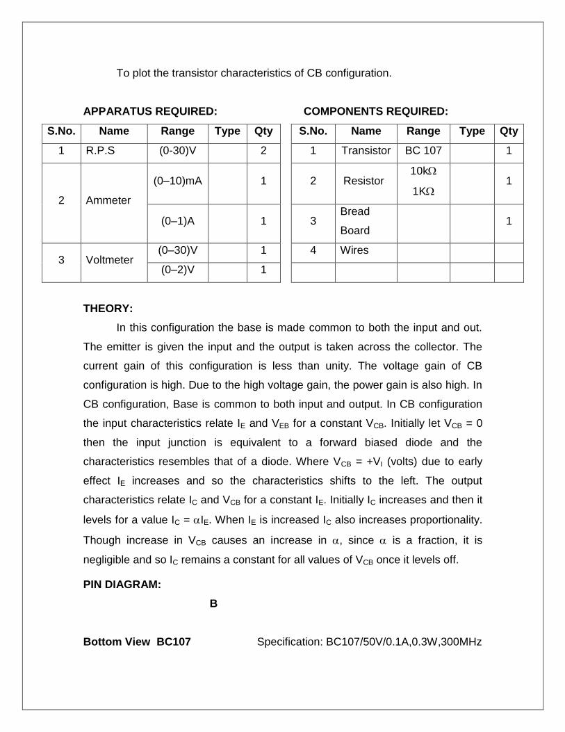
To plot the transistor characteristics of CB configuration.
APPARATUS REQUIRED: COMPONENTS REQUIRED:
S.No. Name Range Type Qty
S.No. Name Range Type Qty
1 R.P.S (0-30)V 2 1 Transistor BC 107 1
2 Ammeter
(0–10)mA 1 2 Resistor 10k
1K
1
(0–1)A 1 3 Bread
Board
1
3 Voltmeter (0–30)V 1 4 Wires
(0–2)V 1
THEORY:
In this configuration the base is made common to both the input and out.
The emitter is given the input and the output is taken across the collector. The
current gain of this configuration is less than unity. The voltage gain of CB
configuration is high. Due to the high voltage gain, the power gain is also high. In
CB configuration, Base is common to both input and output. In CB configuration
the input characteristics relate IE and VEB for a constant VCB. Initially let VCB = 0
then the input junction is equivalent to a forward biased diode and the
characteristics resembles that of a diode. Where VCB = +VI (volts) due to early
effect IE increases and so the characteristics shifts to the left. The output
characteristics relate IC and VCB for a constant IE. Initially IC increases and then it
levels for a value IC = IE. When IE is increased IC also increases proportionality.
Though increase in VCB causes an increase in , since is a fraction, it is
negligible and so IC remains a constant for all values of VCB once it levels off.
PIN DIAGRAM:
B
Bottom View BC107 Specification: BC107/50V/0.1A,0.3W,300MHz

(0-30)V
(0-1)mA
+ -
+
(0-30)mA
+ -
+
+
-
+
+
-
+
+
-
+
(0-2)V (0-30)V (0-30)V
E C
CIRCUIT DIAGRAM:
-
PROCEDURE:
INPUT CHARACTERISTICS:
It is the curve between emitter current IE and emitter-base voltage VBE at
constant collector-base voltage VCB.
1. Connect the circuit as per the circuit diagram.
2. Set VCE=5V, vary VBE in steps of 0.1V and note down the corresponding
IB. Repeat the above procedure for 10V, 15V.
3. Plot the graph VBE Vs IB for a constant VCE.
4. Find the h parameters.
OUTPUT CHARACTERISTICS:
It is the curve between collector current IC and collector-base voltage VCB at
constant emitter current IE.
1. Connect the circuit as per the circuit diagram.
2. Set IB=20A, vary VCE in steps of 1V and note down the corresponding IC.
Repeat the above procedure for 40A, 80A, etc.
3. Plot the graph VCE Vs IC for a constant IB.
4. Find the h parameters
a
a
a
a
a
A
A
A
10 K
a
a
a
a
a
A
A
A
a
a
a
a
a
A
A
A
a
a
a
a
a
A
A
A
a
a
a
a
a
A
A
A
a
a
a
a
a
A
A
A
1K
VEB
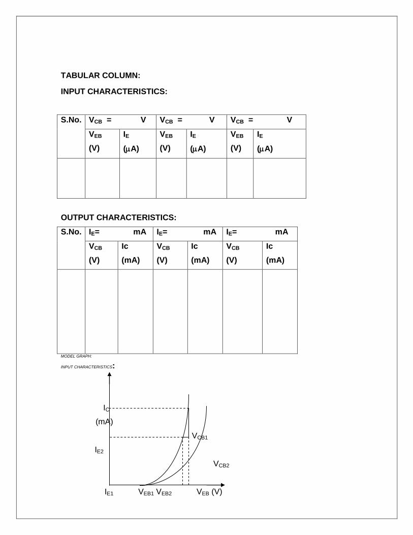
TABULAR COLUMN:
INPUT CHARACTERISTICS:
S.No. VCB = V VCB = V VCB = V
VEB
(V)
IE
(A)
VEB
(V)
IE
(A)
VEB
(V)
IE
(A)
OUTPUT CHARACTERISTICS:
S.No. IE= mA IE= mA IE= mA
VCB
(V)
Ic
(mA)
VCB
(V)
Ic
(mA)
VCB
(V)
Ic
(mA)
MODEL GRAPH:
INPUT CHARACTERISTICS:
IC
(mA)
VCB1
IE2
VCB2
IE1 VEB1 VEB2 VEB (V)
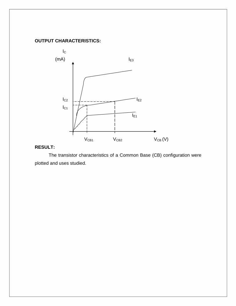
OUTPUT CHARACTERISTICS:
IC
(mA) IE3
IC2 IE2
IC1
IE1
VCB1 VCB2 VCB (V)
RESULT:
The transistor characteristics of a Common Base (CB) configuration were
plotted and uses studied.
Ex.No.2c
CHARACTERISTICS OF CC CONFIGURATION USING BJT
AIM:
To plot the transistor characteristics of CE configuration.
APPARATUS REQUIRED: COMPONENTS REQUIRED:
S.No. Name Range Type Qty
S.No. Name Range Type Qty
1 R.P.S (0-30)V 2 1 Transistor BC 107 1
2 Ammeter
(0–30)mA 1 2 Resistor 1k 2
(0–250)µA 1 3 Bread
Board
1
3 Voltmeter (0–30)V 1 4 Wires
(0–5)V 1
THEORY:
A BJT is a three terminal two – junction semiconductor device in which the
conduction is due to both the charge carrier. Hence it is a bipolar device and it
amplifier the sine waveform as they are transferred from input to output. BJT is
classified into two types – NPN or PNP. A NPN transistor consists of two N
types in between which a layer of P is sandwiched. The transistor consists of
three terminal emitter, collector and base. The emitter layer is the source of the
charge carriers and it is heartily doped with a moderate cross sectional area.
The collector collects the charge carries and hence moderate doping and large
cross sectional area. The base region acts a path for the movement of the
charge carriers. In order to reduce the recombination of holes and electrons the
base region is lightly doped and is of hollow cross sectional area. Normally the
transistor operates with the EB junction forward biased.
In transistor, the current is same in both junctions, which indicates that
there is a transfer of resistance between the two junctions. One to this fact the
transistor is known as transfer resistance of transistor.
Bottom View BC107 Specification: BC107/50V/0.1A,0.3W,300MHz
+
-
+
-
+
+ -
+
+ +
-
+
+
+ -
+
(0-30)mA
(0-250)µA
PIN DIAGRAM:
B
E C
CIRCUIT DIAGRAM:
PROCEDURE:
INPUT CHARECTERISTICS:
1. Connect the circuit as per the circuit diagram.
2. Set VCE, vary VBE in regular interval of steps and note down the
corresponding IB reading. Repeat the above procedure for different values
of VCE.
3. Plot the graph: VBC Vs IB for a constant VCE.
OUTPUT CHARECTERISTICS:
1. Connect the circuit as per the circuit diagram.
A
A V
V
1 K
+
-
+
(0-30)V (0-30)V
(0-30)V (0-30)V
1 K

2. Set IB, Vary VCE in regular interval of steps and note down the
corresponding IC reading. Repeat the above procedure for different
values of IB.
3. Plot the graph: VCE Vs IC for a constant IB.
MODEL GRAPH:
INPUT CHARACTERISTICS: OUTPUT CHARACTERISTICS:
(A) (mA)
IB Ie
VCE=0 VCE=5V IB=60A
IB=40A
IB=20A
0 VBC(V) 0 VCE(V)
TABULAR COLUMN:
INPUT CHARACTERISTICS:
VCE=1V VCE=2V
VBC(V) IB(μA) VBC(V) IB(μA)
OUTPUT CHARACTERISTICS:
IB=20A IB=40A
VCE(V) IE(mA) VCE(V) IE(mA)

RESULT:
The transistor characteristics of a Common Emitter (CC) configuration
were plotted.

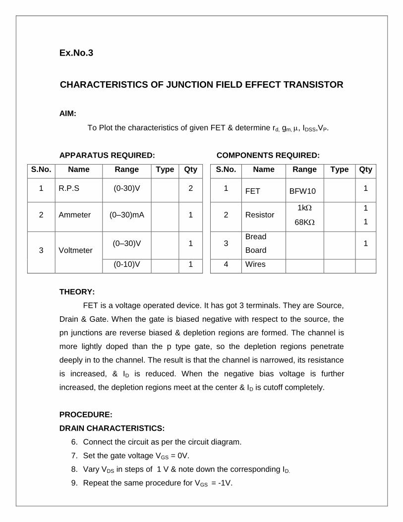
Ex.No.3
CHARACTERISTICS OF JUNCTION FIELD EFFECT TRANSISTOR
AIM:
To Plot the characteristics of given FET & determine rd, gm, , IDSS,VP.
APPARATUS REQUIRED: COMPONENTS REQUIRED:
S.No. Name Range Type Qty
S.No. Name Range Type Qty
1 R.P.S (0-30)V 2 1 FET BFW10 1
2 Ammeter (0–30)mA 1 2 Resistor 1k
68K
1
1
3 Voltmeter (0–30)V 1 3
Bread
Board
1
(0-10)V 1 4 Wires
THEORY:
FET is a voltage operated device. It has got 3 terminals. They are Source,
Drain & Gate. When the gate is biased negative with respect to the source, the
pn junctions are reverse biased & depletion regions are formed. The channel is
more lightly doped than the p type gate, so the depletion regions penetrate
deeply in to the channel. The result is that the channel is narrowed, its resistance
is increased, & ID is reduced. When the negative bias voltage is further
increased, the depletion regions meet at the center & ID is cutoff completely.
PROCEDURE:
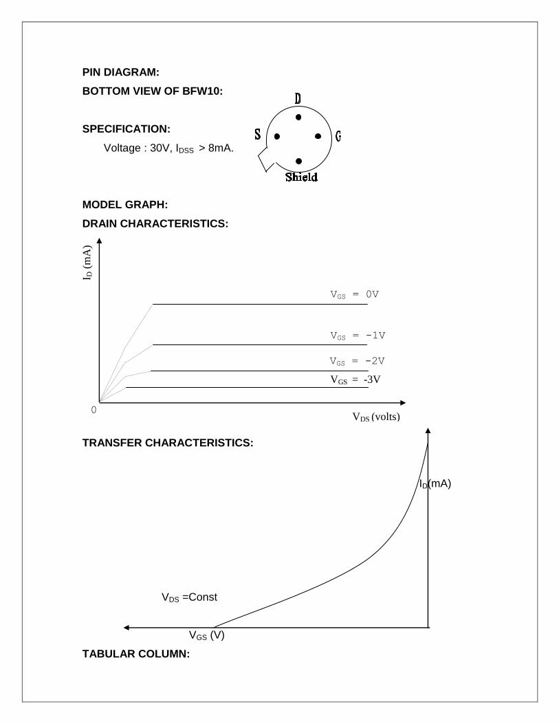
DRAIN CHARACTERISTICS:
1. Connect the circuit as per the circuit diagram.
2. Set the gate voltage VGS = 0V.
3. Vary VDS in steps of 1 V & note down the corresponding ID.
4. Repeat the same procedure for VGS = -1V.

+ (0-30)V
68K
V
+
(0-30)V
(0-30)V
1k (0-30mA)
D G
S
BFW10
-
+ (0-10)V V
A
V
-
5. Plot the graph VDS Vs ID for constant VGS.
OBSERVATIONS
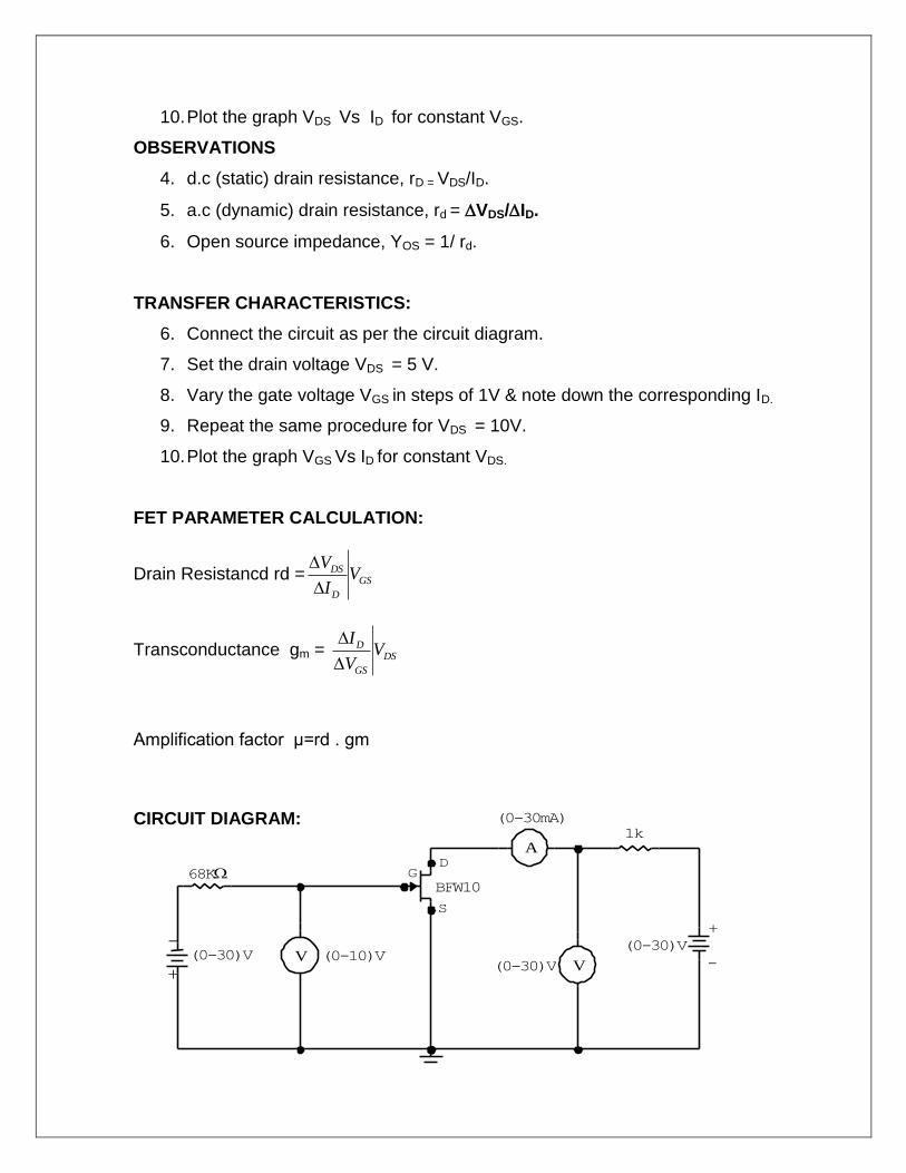
1. d.c (static) drain resistance, rD = VDS/ID.
2. a.c (dynamic) drain resistance, rd = VDS/ID.
3. Open source impedance, YOS = 1/ rd.
TRANSFER CHARACTERISTICS:
1. Connect the circuit as per the circuit diagram.
2. Set the drain voltage VDS = 5 V.
3. Vary the gate voltage VGS in steps of 1V & note down the corresponding ID.
4. Repeat the same procedure for VDS = 10V.
5. Plot the graph VGS Vs ID for constant VDS.
FET PARAMETER CALCULATION:
Drain Resistancd rd = GS
D
DS VI
V
Transconductance gm = DS
GS
D VV
I
Amplification factor μ=rd . gm
CIRCUIT DIAGRAM:
I D (
mA
)
PIN DIAGRAM:
BOTTOM VIEW OF BFW10:
SPECIFICATION:
Voltage : 30V, IDSS > 8mA.
MODEL GRAPH:
DRAIN CHARACTERISTICS:
TRANSFER CHARACTERISTICS:
ID(mA)
VDS =Const
VGS (V)
TABULAR COLUMN:
0
VGS = 0V
VGS = -1V
VGS = -2V
VGS = -3V
VDS (volts)

DRAIN CHARACTERISTICS:
VGS = 0V VGS = -1V
VDS (V) ID(mA) VDS (V) ID(mA)
TRANSFER CHARACTERISTICS:
RESULT:
Thus the Drain & Transfer characteristics of given FET is Plotted.
Rd =
gm =
=
IDSS =
Pinch off voltage VP =
VDS =5volts VDS = 10volts
VGS (V) ID(mA) VGS (V) ID(mA)

Ex.No.4
CHARACTERISTICS OF UNIJUNCTION TRANSISTOR
AIM:
To Plot the characteristics of UJT & determine it’s intrinsic standoff
Ratio.
APPARATUS REQUIRED: COMPONENTS REQUIRED:
S.
No. Name Range Type Qty
S.
No. Name Range Type Qty
1 R.P.S (0-30)V 2 1 UJT 2N2646 1
2 Ammeter (0–30)mA 1
2 Resistor 1K 2
3 Bread
Board
1
3 Voltmeter (0–30)V 1
(0–10)V 1
THEORY:
UJT(Double base diode) consists of a bar of lightly doped n-type silicon
with a small piece of heavily doped P type material joined to one side. It has got
three terminals. They are Emitter(E), Base1(B1),Base2(B2).Since the silicon bar
is lightly doped, it has a high resistance & can be represented as two resistors,
rB1 & rB2. When VB1B2 = 0, a small increase in VE forward biases the emitter
junction. The resultant plot of VE & I E is simply the characteristics of forward
biased diode with resistance. Increasing VEB1 reduces the emitter junction
reverse bias. When VEB1 = VrB1 there is no forward or reverse bias. & IE = 0.
Increasing VEB1 beyond this point begins to forward bias the emitter junction. At
the peak point, a small forward emitter current is flowing. This current is termed
as peak current( IP ). Until this point UJT is said to be operating in cutoff region.
When IE increases beyond peak current the device enters the negative
resistance region. In which the resistance rB1 falls rapidly & VE falls to the valley
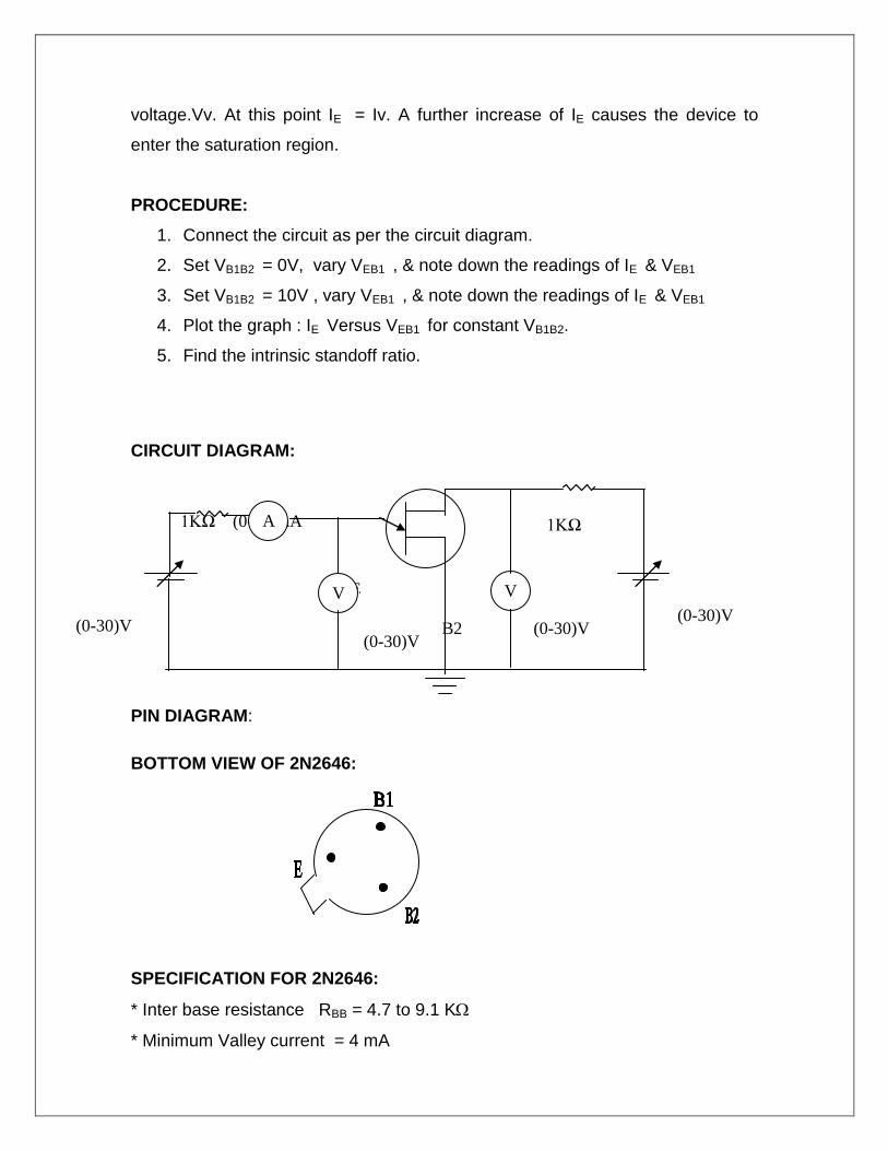
B2
E
voltage.Vv. At this point IE = Iv. A further increase of IE causes the device to
enter the saturation region.
PROCEDURE:
1. Connect the circuit as per the circuit diagram.
2. Set VB1B2 = 0V, vary VEB1 , & note down the readings of IE & VEB1
3. Set VB1B2 = 10V , vary VEB1 , & note down the readings of IE & VEB1
4. Plot the graph : IE Versus VEB1 for constant VB1B2.
5. Find the intrinsic standoff ratio.
CIRCUIT DIAGRAM:
PIN DIAGRAM:
BOTTOM VIEW OF 2N2646:
SPECIFICATION FOR 2N2646:
* Inter base resistance RBB = 4.7 to 9.1 K
* Minimum Valley current = 4 mA
B2
(0-30)V (0-30)V
(0-30)V
1KΩ 1KΩ
(0-30)V
(0-30)mA
V V
A

* Maximun Peak point emitter current 5 A
*Maximum emitter reverse current 12 A.
FORMULA FOR INTRINSIC STANDOFF RATIO:
= VP - VD/ VB1B2., where VD = 0.7V.
MODEL GRAPH:
Peak point
VP
IP
Negative resistance region
VEB1(V)
Valley point VB1B2 = V
VB1B2 = 0V
IV IE (mA)
TABULAR COLUMN:
VB1B2 = 0V VB1B2 = 10V
VEB1 (V) IE (mA) VEB1 (V) IE (mA)

PROCEDURE:
1. Give the circuit connections as per the circuit diagram.
2. The dc input voltage is set to 20 V in RPS.
3. The output sweep waveform is measured using CRO.
4. The graph of output sweep waveform is plotted
RESULT:
1. Thus the characteristics of given UJT was Plotted & its intrinsic standoff
Ratio = ----.
Ex.No.5
CHARACTERISTICS OF PHOTO-DIODE AND
PHOTOTRANSISTOR
AIM:
1. To study the characteristics of a photo-diode.
2. To study the characteristics of phototransistor.
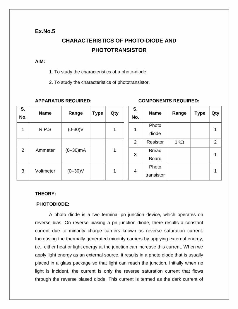
APPARATUS REQUIRED: COMPONENTS REQUIRED:
S.
No. Name Range Type Qty
S.
No. Name Range Type Qty
1 R.P.S (0-30)V 1 1 Photo
diode 1
2 Ammeter (0–30)mA 1
2 Resistor 1K 2
3 Bread
Board 1
3 Voltmeter (0–30)V 1 4 Photo
transistor 1
THEORY:
PHOTODIODE:
A photo diode is a two terminal pn junction device, which operates on
reverse bias. On reverse biasing a pn junction diode, there results a constant
current due to minority charge carriers known as reverse saturation current.
Increasing the thermally generated minority carriers by applying external energy,
i.e., either heat or light energy at the junction can increase this current. When we
apply light energy as an external source, it results in a photo diode that is usually
placed in a glass package so that light can reach the junction. Initially when no
light is incident, the current is only the reverse saturation current that flows
through the reverse biased diode. This current is termed as the dark current of

(0-30)mA
(0-30)V (0-30)V
the photo diode. Now when light is incident on the photo diode then the thermally
generated carriers increase resulting in an increased reverse current which is
proportional to the intensity of incident light. A photo diode can turn on and off at
a faster rate and so it is used as a fast acting switch.
CIRCUIT DIAGRAM:
TABULAR COLUMN:
MODEL GRAPH:
THEORY:
S.No. VOLTAGE
(In Volts)
CURRENT
(In mA)
R
(K)
Illumination lm/m2
1K a
a
a
a
a
A
A
A

IC
PHOTOTRANSISTOR:
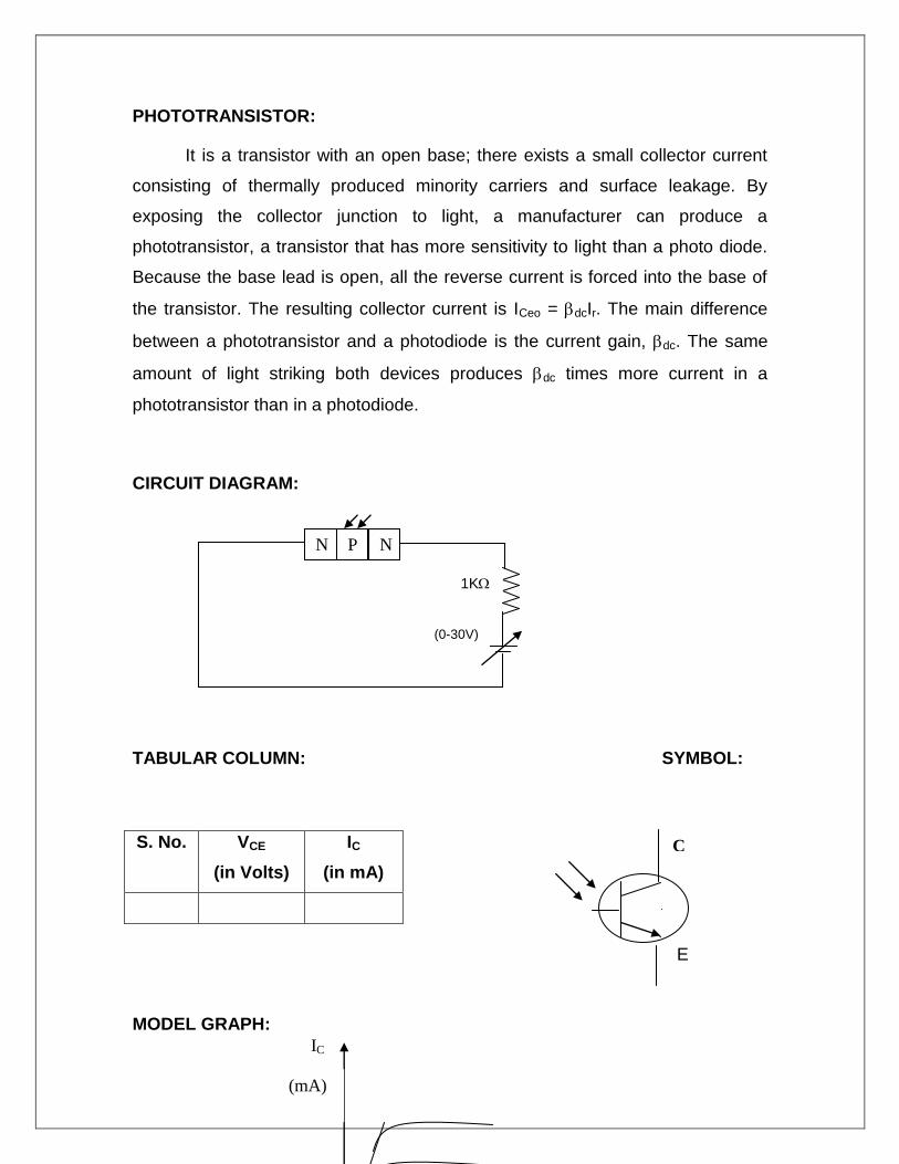
It is a transistor with an open base; there exists a small collector current
consisting of thermally produced minority carriers and surface leakage. By
exposing the collector junction to light, a manufacturer can produce a
phototransistor, a transistor that has more sensitivity to light than a photo diode.
Because the base lead is open, all the reverse current is forced into the base of
the transistor. The resulting collector current is ICeo = dcIr. The main difference
between a phototransistor and a photodiode is the current gain, dc. The same
amount of light striking both devices produces dc times more current in a
phototransistor than in a photodiode.
CIRCUIT DIAGRAM:
TABULAR COLUMN: SYMBOL:
E
MODEL GRAPH:
S. No. VCE
(in Volts)
IC
(in mA)
N P N
1K
(0-30V)
C
(mA)

400 Lux
200 Lux
0 Lux
VCE(V)
PROCEDURE:
PHOTO DIODE:
1. Rig up the circuit as per the circuit diagram.
2. Maintain a known distance (say 5 cm) between the DC bulb and
the photo diode.
3. Set the voltage of the bulb (say, 2V), vary the voltage of the diode
insteps of 1V and note down the corresponding diode current, Ir.
4. Repeat the above procedure for the various voltages of DC bulb.
5. Plot the graph: VD vs. Ir for a constant DC bulb voltage.
PHOTOTRANSISTOR:
1. Rig up the circuit as per the circuit diagram.
2. Maintain a known distance (say 5 cm) between the DC bulb and the
phototransistor.
3. Set the voltage of the bulb (say, 2V), vary the voltage of the diode
in steps of 1V and note down the corresponding diode current, Ir.
4. Repeat the above procedure for the various values of DC bulb.
5. Plot the graph: VD vs. Ir for a constant bulb voltage.
RESULT:
Thus the characteristics of photo diode and phototransistor are studied.

Ex.No.6
CHARACTERISTICS OF THERMISTOR
AIM:
To study the characteristics of Thermistor.
THEORY:
Thermistor or Thermal resistor is two – terminal semiconductor device
whose resistance is temperature sensitive. The value of such resistors decreases
with increase in temperature. Materials employed in the manufacture of the
thermistors include oxides of cobalt, nickel, copper, iron uranium and
manganese.
The thermistors has very high temperature coefficient of resistance, of the
order of 3 to 5% per C, making it an ideal temperature transducer. The
temperature coefficient of resistance is normally negative. The reistance at any
temperature T, is given approximately by
RT = Ro exp β (1/T – 1/To)
Where RT = thermistor resistance at temperature T (K), RO = thersmistor
resistance at temperature To (K), and = a constant determined by calibration.
At high temperatures, this equation reduces to
RT = Ro exp ( β/T)
The resistance – temperature characteristics is shown in Fig 21.10. The
curve is non – linear and the drop in resistance from 5000 to 10 occurs for an
increase in temperature from 20 to 100 C. The temperature of the device can
be changed internally or externally. An increase in current through the device will
raise its temperature carrying a drop in its terminal resistance. Any externally
heat source will result in an increase in its body temperature and drop in

resistance this type action (internal or external) lends itself well to control
mechanism.
Three useful parameters for characterizing the thermistor are the time
constant, dissipation constant , and resistance ratio. The time constant is the
time for a thermistor to change its resistance by 63% of its initial value, for zero –
power dissipation. Typical values of time constant range from 1 to 50 s.
SYMBOL:
MODEL GRAPH:
The dissipation factor is the power necessary to increase the temperature
of a thermistor by 1˚C. Typical values of dissipation factor range from 1 to 10
mW/˚C.
Resistance ratio is the ratio of the resistance at 25 ˚C. Its range is
approximately
3 – 60.
R
(-cm)
T (deg)
T

Thermistors are used measure temperature, flow pressure, liquid level,
voltage or power level, vacuum, composition of gases and thermal conductivity
and also in compensation network.
RESULT:
Thus the Characteristics of thermistor was studied.

Ex.No.7a
SINGLE PHASE HALF WAVE RECTIFIER
AIM:
To construct a Half wave rectifier using diode and to draw its performance
characteristics.
APPARATUS REQUIRED: COMPONENTS
REQUIRED:
S.
No. Name Range Type Qty
S.
No. Name Range Type Qty
1 Transformer 230/(6-0-6)V 1 1
Diode IN4001 1
2 R.P.S (0-30)V 2
3 Ammeter
(0–30)mA 1 2 Resistor 1K 1
(0–250)µA 1 3 Bread
Board
1
4 Voltmeter (0–30)V 1 4 Capacitor 100µf 1
(0–2)V 1 5 CRO 1
FORMULAE:
WITHOUT FILTER:
(i) Vrms = Vm / 2
(ii) Vdc = Vm /
(iii) Ripple Factor = (Vrms / Vdc)2 – 1
(iv) Efficiency = (Vdc / Vrms)2 x 100
WITH FILTER:
(i) Vrms = (Vrms’2 + Vdc
2)
(ii) Vrms’ = Vrpp / (3 x 2)
(iii) Vdc = Vm – V rpp / 2
(iv) Ripple Factor = Vrms’/ Vdc
PROCEDURE:

WITHOUT FILTER:
1. Give the connections as per the circuit diagram.
2. Give 230v, 50HZ I/P to the step down TFR where secondary connected to
the Rectifier I/P.
3. Take the rectifier output across the Load.
4. Plot its performance graph.
WITH FILTER:
1. Give the connections as per the circuit diagram.
2. Give 230v, 50HZ I/P to the step down TFR where secondary connected to
the Rectifier I/P.
3. Connect the Capacitor across the Load.
4. Take the rectifier output across the Load.
5. Plot its performance graph.
CIRCUIT DIAGRAM:
1 Transformer
230 V / 6V 1N 4007
1K 100F 1, 230V,
50Hz
AC supply
CRO
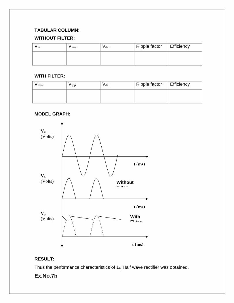
TABULAR COLUMN:
WITHOUT FILTER:
Vm Vrms Vdc Ripple factor Efficiency
WITH FILTER:
Vrms Vrpp Vdc Ripple factor Efficiency
MODEL GRAPH:
RESULT:
Thus the performance characteristics of 1 Half wave rectifier was obtained.
Ex.No.7b
Vin
(Volts)
t (ms)
Vo
(Volts)
t (ms)
t (ms)
Vo
(Volts)
Without Filter
With Filter

SINGLE PHASE FULL WAVE RECTIFIER
AIM:
To construct a Full wave rectifier using diode and to draw its performance
characteristics.
APPARATUS REQUIRED: COMPONENTS
REQUIRED:
S.
No. Name Range Type Qty
S.
No. Name Range Type Qty
1 Transformer 230/(6-0-6)V 1 1
Diode IN4001 2
2 R.P.S (0-30)V 2
3 Ammeter
(0–30)mA 1 2 Resistor 1K 1
(0–250)µA 1 3 Bread
Board
1
4 Voltmeter (0–30)V 1 4 Capacitor 100µf 1
(0–2)V 1 5 CRO 1
FORMULAE:
WITHOUT FILTER:
(i) Vrms = Vm / 2
(ii) Vdc = 2Vm /
(iii) Ripple Factor = (Vrms / Vdc)2 – 1
(iv) Efficiency = (Vdc / Vrms)2 x 100
WITH FILTER:
(i) Vrms = Vrpp /(2* 3)
(ii) Vdc = Vm – V rpp
(iv) Ripple Factor = Vrms’/ Vdc
PROCEDURE:
WITHOUT FILTER:
1. Give the connections as per the circuit diagram.

2. Give 230v, 50HZ I/P to the step down TFR where secondary connected
to the Rectifier I/P.
3. Take the rectifier output across the Load.
4. Plot its performance graph.
WITH FILTER:
1. Give the connections as per the circuit diagram.
2. Give 230v, 50HZ I/P to the step down TFR where secondary connected to
the Rectifier I/P.
3. Connect the Capacitor across the Load.
4. Take the rectifier output across the Load.
5. Plot its performance graph.
CIRCUIT DIAGRAM:
1N 4007
1K 100F
1, 230V,
50Hz
AC supply
CRO
1N 4007
1 Transformer
230 V / 6V

TABULAR COLUMN:
WITHOUT FILTER:
Vm Vrms Vdc Ripple factor Efficiency
WITH FILTER:
Vrms Vrpp Vdc Ripple factor Efficiency
MODEL GRAPH :
RESULT: Thus the performance characteristics of 1 Full wave rectifier were
obtained.
Ex.No.8
Vin
(Volts)
t (ms)
Vo
(Volts)
t (ms)
t (ms)
Vo
(Volts)
Without Filter
With Filter

DIFFERENTIAL AMPLIFIER
AIM:
To construct a Differential amplifier in Common mode & Differential mode
configuration and to find common mode rejection ratio.
APPARATUS REQUIRED: COMPONENTS REQUIRED:
Apparatus Range Qty
1 RPS (0-30)V 1
2 CRO 1
3 Signal
Generator 1
4 DCB 2
5 DRB 2
THEORY:
The Differential amplifier circuit is an extremely popular connection used in
IC units. The circuit has separate inputs , two separate outputs and emitters are
connected together. If the same input is applied to both inputs, the operation is
called common mode. In double ended operation two input signals are applied ,
the difference of the inputs resulting in outputs from both collectors due to the
difference of the signals applied to both the inputs. The main feature of the
differential amplifier is the very large gain when opposite signals are applied to
inputs as compared to small signal resulting from common input. The ratio of this
difference gain to the common gain is called common mode rejection ratio.
CIRCUIT DIAGRAM:
DIFFERENTIAL MODE:
S.No Item Type Range Qty
1 Transistor BC107 1
2 Capacitor 470F 1
3 Resistor 3.9KΩ
3.3KΩ
1
1
4 Bread board 1

COMMON MODE:
9V
3.3 K
3.9K
Vo1 Vo2
V2
13V
3.9K
-9V
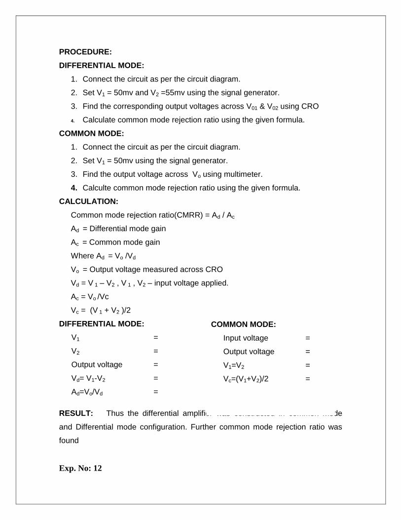
PROCEDURE:
DIFFERENTIAL MODE:
1. Connect the circuit as per the circuit diagram.
2. Set V1 = 50mv and V2 =55mv using the signal generator.
3. Find the corresponding output voltages across V01 & V02 using CRO
4. Calculate common mode rejection ratio using the given formula.
COMMON MODE:
1. Connect the circuit as per the circuit diagram.
2. Set V1 = 50mv using the signal generator.
3. Find the output voltage across Vo using multimeter.
4. Calculte common mode rejection ratio using the given formula.
CALCULATION:
Common mode rejection ratio(CMRR) = Ad / Ac
Ad = Differential mode gain
Ac = Common mode gain
Where Ad = Vo /Vd
Vo = Output voltage measured across CRO
Vd = V 1 – V2 , V 1 , V2 – input voltage applied.
Ac = Vo /Vc
Vc = (V 1 + V2 )/2
DIFFERENTIAL MODE:
V1 =
V2 =
Output voltage =
Vd= V1-V2 =
Ad=Vo/Vd =
RESULT: Thus the differential amplifier was constructed in common mode
and Differential mode configuration. Further common mode rejection ratio was
found
Exp. No: 12
COMMON MODE:
Input voltage =
Output voltage =
V1=V2 =
Vc=(V1+V2)/2 =
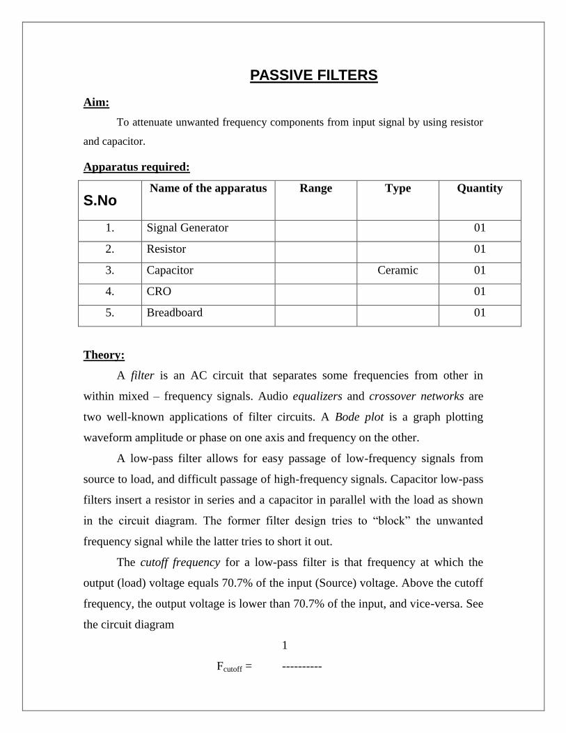
PASSIVE FILTERS
Aim:
To attenuate unwanted frequency components from input signal by using resistor
and capacitor.
Apparatus required:
S.No Name of the apparatus Range Type Quantity
1. Signal Generator 01
2. Resistor 01
3. Capacitor Ceramic 01
4. CRO 01
5. Breadboard 01
Theory:
A filter is an AC circuit that separates some frequencies from other in
within mixed – frequency signals. Audio equalizers and crossover networks are
two well-known applications of filter circuits. A Bode plot is a graph plotting
waveform amplitude or phase on one axis and frequency on the other.
A low-pass filter allows for easy passage of low-frequency signals from
source to load, and difficult passage of high-frequency signals. Capacitor low-pass
filters insert a resistor in series and a capacitor in parallel with the load as shown
in the circuit diagram. The former filter design tries to “block” the unwanted
frequency signal while the latter tries to short it out.
The cutoff frequency for a low-pass filter is that frequency at which the
output (load) voltage equals 70.7% of the input (Source) voltage. Above the cutoff
frequency, the output voltage is lower than 70.7% of the input, and vice-versa. See
the circuit diagram
1
Fcutoff = ----------

2RC
A high-pass filter allows for easy passage of high-frequency signals from source to
load, and difficult passage of low-frequency signals. Capacitor high-pass filters
insert a capacitor in series with the load as shown in the circuit diagram. The
former filter design tries to “brick” the unwanted frequency signal while the latter
tries to short it out.
The cutoff frequency for a high-pass filter is that frequency at which the
output (load) voltage equals 70.7% of the input (source) voltage. Above the cutoff
frequency, the output voltage is greater than 70.7% of the input, and vice-versa.
1
Fcutoff = ----------
2RC
A band – pass filter works to screen out frequencies that are too low or too
high, giving easy passage only to frequencies within a certain range. Stacking a
low-pass filter on the end of a high-pass filter, or vice-versa can make band-pass
filters. Refer the circuit diagrams
Fig. 7.6
“Attenuate” means to reduce or diminish in amplitude. When you
turn down the volume control on your stereo, you are “attenuating” the signal
being sent to the speakers.
A band-stop filter works to screen out frequencies that are within a certain
range, giving easy passage only to frequencies outside of that range. Also known
as band-elimination, band-reject, or notch filters.
Placing a low-pass filter in parallel with a high-pass filter can make band-
stop filters. Commonly, both the low-pass and high-pass filter sections are of the
Signal
input
Low-pass filter High-pass filter Signal
output Blocks frequencies
that are too high
Blocks frequencies
that are too low

Signal
Input
Low-pass filter
High-pass filter
Signal
Output
“T” configuration giving the name “Twin-T” to the band-stop combination. Refer
the fig.7.7, 7.8a and 7.8b.
Passes low frequencies
Passes high frequencies
Fig. 7.8a
The frequency of maximum attenuation is called the notch
frequency.
Procedure:
1. Give the connections as per circuit diagrams.
2. Switch on the main.
3. Change the frequency from minimum and find the output
voltage by using CRO.
4. Draw the graph.
5. Verify the cut off frequency.
6. Switch off the main.
Result:
Thus we analyze passive filter and various waveforms are noted
Exp. No : 10
STUDY OF CRO AND
POWER FACTOR MEASUREMENT USING CRO
Aim:
To study cathode Ray Oscilloscope (CRO) and measurement of power factor using
CRO.

Apparatus required:
S.No Name of the apparatus Range Type Quantity
1. Resistance Box 1
2. Capacitance Box 1
3. Inductance Box 1
4. Function Generator 1
5. Bread board 1
Theory:
The cathode ray oscilloscope is the most versatile measuring instrument
available. We can measure following parameters using the CRO:
1. AC or DC voltage.
2. Time (t=1/f).
3. Phase relationship
4. Waveform calculation: Rise time; fall time; on time; off-time
Distortion, etc.
We can also measure non-electrical physical quantities like pressure, strain,
temperature, acceleration, etc., by converting into electrical quantities using
a transducer.
Major blocks:
1. Cathode ray tube (CRT)
2. Vertical amplifier
3. Horizontal amplifier
4. Sweep generator
5. Trigger circuit
6. Associated power supply.

1. The cathode ray tube is the heart of CRO. The CRT is enclosed in an
evacuated glass envelope to permit the electron beam to traverse in the
tube easily. The main functional units of CRO are as follows.
Electron gun assembly
Deflection plate unit
Screen.
2. Vertical Amplifier is the main factor in determining the bandwidth and
sensitivity of an oscilloscope. Vertical sensitivity is a measure of how
much the electron beam will be deflected for a specified input signal.
On the front panel of the oscilloscope, one can see a knob attached to a
rotary switch labeled volts/division. The rotary switch is electrically
connected to the input attenuation network. The setting of the rotary
switch indicates what amplitude signal is required to deflect the beam
vertically by one division.
3. Horizontal amplifier Under normal mode of operation, the horizontal
amplifier will amplify the sweep generator input. When the CRO is
being used in the X-Y mode, the horizontal amplifier will amplify the
signal applied to the horizontal input terminal. Although the vertical
amplifier mush be able to faithfully reproduce low-amplitude and high
frequency signal with fast rise-time, the horizontal amplifier is only
required to provide a faithful reproduction of the sweep signal which
has a relatively high amplitude and slow rise time.
4. Sweep generator and Trigger circuit These two units form the Signal
Synchronization unit of the CRO.
5. Associated Power Supply: The input signal may come from an
external source when the trigger selector switch is set to EXT or from
low amplitude AC voltage at line frequency when the switch is set to
LINE or from the vertical amplifier when the switch is set to INT. When
set for INT (internal triggering), the trigger circuit receives its inputs
from the vertical amplifier.

Major Blocks in a Practical CRO
A CRO consists of a cathode ray tube (CRT) and additional control knobs.
The main parts of a CRT are:
1. Electron gun assembly.
2. Deflection plate assembly.
3. Fluorescent screen.
Electron Gun Assembly: The electron gun assembly produces a sharp beam of
electrons, which are accelerated to high velocity. This focused beam of electrons
strike the fluorescent screen with sufficient energy to cause a luminous spot on the
screen.
Deflection plate assembly: This part consists of two plates in which one pair of
plates is placed horizontally and other of plates is placed vertically. The signal
under test is applied to vertical deflecting plates. The horizontal deflection plates
are connected to a built-in ramp generator, which moves the luminous spot
periodically in a horizontal direction from left to right over the screen. These two
deflection plates give stationary appearance to the waveform on the screen. CRO
operates on voltage. Since the deflection of the electron beam is directly
proportional to the deflecting voltage, the CRT may be used as a linear measuring
device. The voltage being measured is applied to the vertical plates through an
iterative network, whose propagation time corresponds to the velocity of electrons,
thereby synchronizing the voltage applied to the vertical plate with the velocity of
the beam.
Synchronization of input signal: The sweep generator produces a saw tooth
waveform, which is used to synchronize the applied voltage to obtain a stationary-
applied signal. This requires that the time base be operated at a submultiples
frequency of the signal under measurement. If synchronization is not done, the
pattern is not stationary, but appears to drift across the screen in a random fashion.
Internal synchronization This trigger is obtained from the time base generator to
synchronize the signal.
External synchronization An external trigger source can also be used to
synchronize the signal being measured.
Auto Triggering Mode The time base used in this case in a self-oscillating
condition, i.e., it gives an output even in the absence of any Y-input. The
advantage of this mode is that the beam is visible on the screen under all
conditions, including the zero input. When the input exceeds a certain magnitude
then the internal free running oscillator locks on to the frequency.
Precautions:
1. The ammeter is connected using thick wires.
2. While reversing ammeter polarity, see to it that the capacitor is not
discharged.
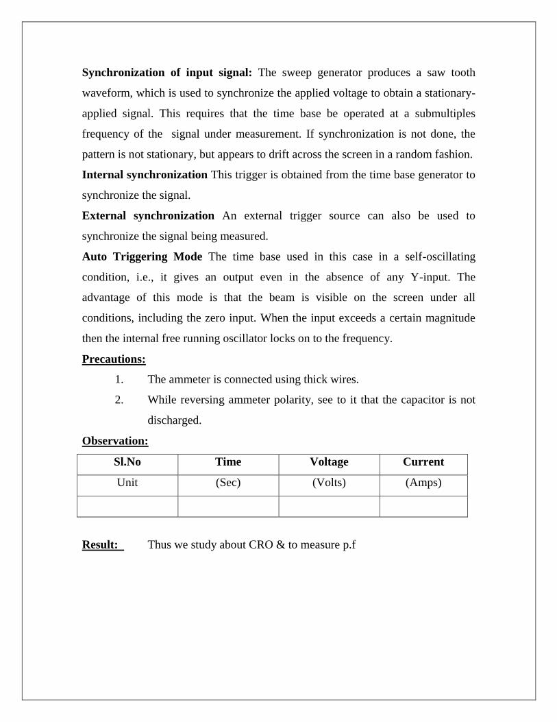
Observation:
Sl.No Time Voltage Current
Unit (Sec) (Volts) (Amps)
Result: Thus we study about CRO & to measure p.f

CLASS : II YEAR/ III SEMSESTER
SUBJECT CODE : 131351
SUBJECT : ELECTRON DEVICES AND CIRCUITS LAB
BATCH : A2
STAFF IN-CHARGE: Mrs. V. GEETHA PRIYA
DESIGNATION : ASSISTANT PROFESSOR
STAFF CODE : EE52
LIST OF EXPERIMENTS
131351 ELECTRON DEVICES AND CIRCUITS LABORATORY L T P C (B.E. (EEE), B.E. (E&I) and B.E. (I & C) 0 0 3 2 (Revised)
13. Characteristics of semiconductor diode and zener diode .
14. Characteristics of transistor under CE, CB and CC .
15. Characteristics of FET .
16. Characteristics of UJT .
17. Characteristics of SCR, DIAC and TRIAC.
18. Photodiode, Phototransistor characteristics and study of light
activated relay circuit.
19. Static characteristics of Thermistors.
20. Single phase half wave and full wave rectifiers with inductive and
capacitive filters.
21. Differential amplifiers using FET.
22. Study of CRO.
23. Series and parallel resonance circuits.
24. Realization of passive filters.
Ex.No.1a
CHARACTERISTICS OF PN JUNCTION DIODE
AIM:
To study the PN junction diode characteristics under Forward & Reverse
bias conditions.
APPARATUS REQUIRED: COMPONENTS REQUIRED:
S.No. Name Range Type Qty
S.No. Name Range Type Qty
1 R.P.S 1 Diode
2 Ammeter
2 Resistor
3 Bread
Board
3 Voltmeter 4 Wires
THEORY:
A PN junction diode is a two terminal junction device. It conducts only in
one direction (only on forward biasing).
FORWARD BIAS:
On forward biasing, initially no current flows due to barrier potential. As the
applied potential exceeds the barrier potential the charge carriers gain sufficient
energy to cross the potential barrier and hence enter the other region. The holes,
which are majority carriers in the P-region, become minority carriers on entering
the N-regions, and electrons, which are the majority carriers in the N-region,
become minority carriers on entering the P-region. This injection of Minority

carriers results in the current flow, opposite to the direction of electron
movement.

REVERSE BIAS:
On reverse biasing, the majority charge carriers are attracted towards the
terminals due to the applied potential resulting in the widening of the depletion
region. Since the charge carriers are pushed towards the terminals no current
flows in the device due to majority charge carriers. There will be some current in
the device due to the thermally generated minority carriers. The generation of
such carriers is independent of the applied potential and hence the current is
constant for all increasing reverse potential. This current is referred to as
Reverse Saturation Current (IO) and it increases with temperature. When the
applied reverse voltage is increased beyond the certain limit, it results in
breakdown. During breakdown, the diode current increases tremendously.
PROCEDURE:
FORWARD BIAS:
5. Connect the circuit as per the diagram.
6. Vary the applied voltage V in steps of 0.1V.
7. Note down the corresponding Ammeter readings I.
8. Plot a graph between V & I
OBSERVATIONS
4. Find the d.c (static) resistance = V/I.
5. Find the a.c (dynamic) resistance r = V / I (r = V/I) = 12
12
II
VV
.
6. Find the forward voltage drop = [Hint: it is equal to 0.7 for Si and 0.3 for
Ge]
REVERSE BIAS:
6. Connect the circuit as per the diagram.
7. Vary the applied voltage V in steps of 1.0V.
8. Note down the corresponding Ammeter readings I.
9. Plot a graph between V & I
10. Find the dynamic resistance r = V / I.
(0-100)mA, MC
+ -
+
+
-
+
(0-15)V, MC +
-
+
(0-10)V
RPS
(0-500)µA,MC
+ -
+
+
-
+
(0-30)V, MC +
-
+
(0-30)V
RPS
FORMULA FOR REVERSE SATURATION CURRENT (IO):
Io = I/[exp(V/VT)]-1
Where VT is the voltage equivalent of Temperature = kT/q
-k is Boltzmann’s constant, q is the charge of the electron and T is the
temperature in degrees Kelvin.
=1 for Silicon and 2 for Germanium
CIRCUIT DIAGRAM:
FORWARD BIAS:
REVERSE BIAS:
Specification for 1N4001: Silicon Diode
Peak Inverse Voltage: 50V
470 a
a
a
a
a
A
A
A
470 a
a
a
a
a
A
A
A
Idc = 1A.
Maximum forward voltage drop at 1 Amp is 1.1 volts
Maximum reverse current @50 volts is 5A
TABULAR COLUMN:
FORWARD BIAS: REVERSE BIAS:
MODEL GRAPH
If (mA)
I2
Vb I1
( Volts) V1 V2 Vf
(Volts)
Ir (A)
RESULT:
Forward and Reverse bias characteristics of the PN junction diode and the
dynamic resistance under
S.No. VOLTAGE
(In Volts)
CURRENT
(In mA)
S..No. VOLTAGE
(In Volts)
CURRENT
(In A)

i) Forward bias = ---------------------
ii) Reverse bias = ----------------------.
iii) Reverse Saturation Current = ----------------.
Ex.No.1b
CHARACTERISTICS OF ZENER DIODE
AIM:
To determine the breakdown voltage of a given zener diode.
APPARATUS REQUIRED: COMPONENTS REQUIRED:
S.No. Name Range Type Qty
S.No. Name Range Type Qty
1 R.P.S 1 zener
diode
2 Ammeter
2 Resistor
3 Bread
Board
3 Voltmeter 4 Wires
THEORY:
A properly doped crystal diode, which has a sharp breakdown voltage, is known
as zener diode.
FORWARD BIAS:
On forward biasing, initially no current flows due to barrier potential. As the
applied potential increases, it exceeds the barrier potential at one value and the
charge carriers gain sufficient energy to cross the potential barrier and enter the
other region. the holes ,which are majority carriers in p-region, become minority
carriers on entering the N-regions and electrons, which are the majority carriers
in the N-regions become minority carriers on entering the P-region. This injection
of minority carriers results current, opposite to the direction of electron
movement.
REVERSE BIAS:
When the reverse bias is applied due to majority carriers small amount of
current (ie) reverse saturation current flows across the junction. As the reverse
bias is increased to breakdown voltage, sudden rise in current takes place due to
zener effect.
ZENER EFFECT:
Normally, PN junction of Zener Diode is heavily doped. Due to heavy
doping the depletion layer will be narrow. When the reverse bias is increased the
potential across the depletion layer is more. This exerts a force on the electrons
in the outermost shell. Because of this force the electrons are pulled away from
the parent nuclei and become free electrons. This ionization, which occurs due to
electrostatic force of attraction, is known as Zener effect. It results in large
number of free carriers, which in turn increases the reverse saturation current
PROCEDURE:
FORWARD BIAS:
1. Connect the circuit as per the circuit diagram.
2. Vary the power supply in such a way that the readings are taken in steps
of 0.1V in the voltmeter till the needle of power supply shows 30V.
3. Note down the corresponding ammeter readings.
4. Plot the graph :V (vs) I.
5. Find the dynamic resistance r = V / I.
REVERSE BIAS:
7. Connect the circuit as per the diagram.
8. Vary the power supply in such a way that the readings are taken in steps
of 0.1V in the voltmeter till the needle of power supply shows 30V.
9. Note down the corresponding Ammeter readings I.
10. Plot a graph between V & I
11. Find the dynamic resistance r = V / I.
12. Find the reverse voltage Vr at Iz=20 mA.
CIRCUIT DIAGRAM:

(0-15) V
+ -
+
-
+
-
(0-10) V
(0-10) V, MC
+ -
+
-
+
-
(0-30) V
FORWARD BIAS:
REVERSE BIAS:
1K
a
a
a
a
a
A
A
A
a
a
a
a
a
A
A
A
470
aaaa
aAA
A
aaaa
aAA
A
a
a
a
a
a
A
A
A
(0-10)mA
1
K
a
a
a
a
a
A
A
A
a
a
a
a
a
A
A
A
1K
aaaa
aAA
A
aaaa
aAA
A
a
a
a
a
a
A
A
A
(0-500)μA, MC

ZENER DIODE:
If ( mA)
I2
VB I1
Vr V1 V2 Vf
(V) (V)
Ir (μA)
TABULAR COLUMN:
FORWARD BIAS: REVERSE BIAS:
RESULT:
Forward and Reverse bias characteristics of the zener diode was studied
and
Forward bias dynamic resistance = ---------------------
Reverse bias dynamic resistance = ----------------------
The reverse voltage at Iz =20 mA determined from the reverse
characteristics of the Zener diode is --------------------------.
S..No. VOLTAGE
(In Volts)
CURRENT
(In mA)
S.No. VOLTAGE
(In Volts)
CURRENT
(In A)

Ex. No. 2a
CHARACTERISTICS OF CE CONFIGURATION USING BJT
AIM:
To plot the transistor characteristics of CE configuration.
APPARATUS REQUIRED: COMPONENTS REQUIRED:
S.No. Name Range Type Qty
S.No. Name Range Type Qty
1 R.P.S 1 Transistor
2 Ammeter
2 Resistor
3 Bread
Board
3 Voltmeter 4 Wires
THEORY:
A BJT is a three terminal two – junction semiconductor device in which the
conduction is due to both the charge carrier. Hence it is a bipolar device and it
amplifier the sine waveform as they are transferred from input to output. BJT is
classified into two types – NPN or PNP. A NPN transistor consists of two N
types in between which a layer of P is sandwiched. The transistor consists of
three terminal emitter, collector and base. The emitter layer is the source of the
charge carriers and it is heartily doped with a moderate cross sectional area.
The collector collects the charge carries and hence moderate doping and large
cross sectional area. The base region acts a path for the movement of the
charge carriers. In order to reduce the recombination of holes and electrons the
base region is lightly doped and is of hollow cross sectional area. Normally the
transistor operates with the EB junction forward biased.

Bottom View BC107 Specification: BC107/50V/0.1A,0.3W,300MHz
(0 – 30)mA 1 K
In transistor, the current is same in both junctions, which indicates that
there is a transfer of resistance between the two junctions. One to this fact the
transistor is known as transfer resistance of transistor.
PROCEDURE:
INPUT CHARACTERISTICS:
4. Connect the circuit as per the circuit diagram.
5. Set VCE, vary VBE in regular interval of steps and note down the
corresponding IB reading. Repeat the above procedure for different values of
VCE.
6. Plot the graph: VBE Vs IB for a constant VCE.
OUTPUT CHARACTERISTICS:
4. Connect the circuit as per the circuit diagram.
5. Set IB, Vary VCE in regular interval of steps and note down the
corresponding IC reading. Repeat the above procedure for different
values of IB.
6. Plot the graph: VCE Vs IC for a constant IB.
PIN DIAGRAM:
B
E C
CIRCUIT DIAGRAM:

(0 – 250) A
10 K
- +
BC107
10 KΩ
+
-
+
+
-
+
(0-30)V
+
-
+
+
-
+
+ -
+
(0-30)V
(0-30)V
(0-1)V
MODEL GRAPH:
INPUT CHARACTERISTICS: OUTPUT CHARACTERISTICS:
TABULAR COLUMN:
INPUT CHARACTERISTICS:
A
A
V
V
C
E
C
B
C
VCE = 0V
VCE = 5V
IB
µA mA
VBE(V) VCE(V)
0 0
IB=60A
IB=40A
IB=20A
IC

VCE=1V VCE=2V
VBE(V) IB(μA) VBE(V) IB(μA)
OUTPUT CHARACTERISTICS:
IB=20A IB=40A
VCE(V) IC(mA) VCE(V) IC(mA)
RESULT:
The transistor characteristics of a Common Emitter (CE)
configuration were plotted
Ex.No.2b
CHARACTERISTICS OF CB CONFIGURATION USING BJT
AIM:

To plot the transistor characteristics of CB configuration.
APPARATUS REQUIRED: COMPONENTS REQUIRED:
S.No. Name Range Type Qty
S.No. Name Range Type Qty
1 R.P.S (0-30)V 2 1 Transistor BC 107 1
2 Ammeter
(0–10)mA 1 2 Resistor 10k
1K
1
(0–1)A 1 3 Bread
Board
1
3 Voltmeter (0–30)V 1 4 Wires
(0–2)V 1
THEORY:
In this configuration the base is made common to both the input and out.
The emitter is given the input and the output is taken across the collector. The
current gain of this configuration is less than unity. The voltage gain of CB
configuration is high. Due to the high voltage gain, the power gain is also high. In
CB configuration, Base is common to both input and output. In CB configuration
the input characteristics relate IE and VEB for a constant VCB. Initially let VCB = 0
then the input junction is equivalent to a forward biased diode and the
characteristics resembles that of a diode. Where VCB = +VI (volts) due to early
effect IE increases and so the characteristics shifts to the left. The output
characteristics relate IC and VCB for a constant IE. Initially IC increases and then it
levels for a value IC = IE. When IE is increased IC also increases proportionality.
Though increase in VCB causes an increase in , since is a fraction, it is
negligible and so IC remains a constant for all values of VCB once it levels off.
PIN DIAGRAM:
B
Bottom View BC107 Specification: BC107/50V/0.1A,0.3W,300MHz

(0-30)V
(0-1)mA
+ -
+
(0-30)mA
+ -
+
+
-
+
+
-
+
+
-
+
(0-2)V (0-30)V (0-30)V
E C
CIRCUIT DIAGRAM:
-
PROCEDURE:
INPUT CHARACTERISTICS:
It is the curve between emitter current IE and emitter-base voltage VBE at
constant collector-base voltage VCB.
5. Connect the circuit as per the circuit diagram.
6. Set VCE=5V, vary VBE in steps of 0.1V and note down the corresponding
IB. Repeat the above procedure for 10V, 15V.
7. Plot the graph VBE Vs IB for a constant VCE.
8. Find the h parameters.
OUTPUT CHARACTERISTICS:
It is the curve between collector current IC and collector-base voltage VCB at
constant emitter current IE.
5. Connect the circuit as per the circuit diagram.
6. Set IB=20A, vary VCE in steps of 1V and note down the corresponding IC.
Repeat the above procedure for 40A, 80A, etc.
7. Plot the graph VCE Vs IC for a constant IB.
8. Find the h parameters
a
a
a
a
a
A
A
A
10 K
a
a
a
a
a
A
A
A
a
a
a
a
a
A
A
A
a
a
a
a
a
A
A
A
a
a
a
a
a
A
A
A
a
a
a
a
a
A
A
A
1K
VEB

TABULAR COLUMN:
INPUT CHARACTERISTICS:
S.No. VCB = V VCB = V VCB = V
VEB
(V)
IE
(A)
VEB
(V)
IE
(A)
VEB
(V)
IE
(A)
OUTPUT CHARACTERISTICS:
S.No. IE= mA IE= mA IE= mA
VCB
(V)
Ic
(mA)
VCB
(V)
Ic
(mA)
VCB
(V)
Ic
(mA)
MODEL GRAPH:
INPUT CHARACTERISTICS:

IC
(mA)
VCB1
IE2
VCB2
IE1 VEB1 VEB2 VEB (V)
OUTPUT CHARACTERISTICS:
IC
(mA) IE3
IC2 IE2
IC1
IE1
VCB1 VCB2 VCB (V)
RESULT:
The transistor characteristics of a Common Base (CB) configuration were
plotted and uses studied.
Ex.No.2c
CHARACTERISTICS OF CC CONFIGURATION USING BJT
AIM:
To plot the transistor characteristics of CE configuration.
APPARATUS REQUIRED: COMPONENTS REQUIRED:

Bottom View BC107 Specification: BC107/50V/0.1A,0.3W,300MHz
S.No. Name Range Type Qty
S.No. Name Range Type Qty
1 R.P.S (0-30)V 2 1 Transistor BC 107 1
2 Ammeter
(0–30)mA 1 2 Resistor 1k 2
(0–250)µA 1 3 Bread
Board
1
3 Voltmeter (0–30)V 1 4 Wires
(0–5)V 1
THEORY:
A BJT is a three terminal two – junction semiconductor device in which the
conduction is due to both the charge carrier. Hence it is a bipolar device and it
amplifier the sine waveform as they are transferred from input to output. BJT is
classified into two types – NPN or PNP. A NPN transistor consists of two N
types in between which a layer of P is sandwiched. The transistor consists of
three terminal emitter, collector and base. The emitter layer is the source of the
charge carriers and it is heartily doped with a moderate cross sectional area.
The collector collects the charge carries and hence moderate doping and large
cross sectional area. The base region acts a path for the movement of the
charge carriers. In order to reduce the recombination of holes and electrons the
base region is lightly doped and is of hollow cross sectional area. Normally the
transistor operates with the EB junction forward biased.
In transistor, the current is same in both junctions, which indicates that
there is a transfer of resistance between the two junctions. One to this fact the
transistor is known as transfer resistance of transistor.
PIN DIAGRAM:
B
E C
+
-
+
-
+
+ -
+
+ +
-
+
+
+ -
+
(0-30)mA
(0-250)µA
CIRCUIT DIAGRAM:
PROCEDURE:
INPUT CHARECTERISTICS:
4. Connect the circuit as per the circuit diagram.
5. Set VCE, vary VBE in regular interval of steps and note down the
corresponding IB reading. Repeat the above procedure for different values
of VCE.
6. Plot the graph: VBC Vs IB for a constant VCE.
OUTPUT CHARECTERISTICS:
4. Connect the circuit as per the circuit diagram.
5. Set IB, Vary VCE in regular interval of steps and note down the
corresponding IC reading. Repeat the above procedure for different
values of IB.
6. Plot the graph: VCE Vs IC for a constant IB.
MODEL GRAPH:
INPUT CHARACTERISTICS: OUTPUT CHARACTERISTICS:
A
A V
V
1 K
+
-
+
(0-30)V (0-30)V
(0-30)V (0-30)V
1 K

(A) (mA)
IB Ie
VCE=0 VCE=5V IB=60A
IB=40A
IB=20A
0 VBC(V) 0 VCE(V)
TABULAR COLUMN:
INPUT CHARACTERISTICS:
VCE=1V VCE=2V
VBC(V) IB(μA) VBC(V) IB(μA)
OUTPUT CHARACTERISTICS:
IB=20A IB=40A
VCE(V) IE(mA) VCE(V) IE(mA)
RESULT:

The transistor characteristics of a Common Emitter (CC) configuration
were plotted.
Ex.No.3
CHARACTERISTICS OF JUNCTION FIELD EFFECT TRANSISTOR
AIM:
To Plot the characteristics of given FET & determine rd, gm, , IDSS,VP.
APPARATUS REQUIRED: COMPONENTS REQUIRED:
S.No. Name Range Type Qty
S.No. Name Range Type Qty
1 R.P.S (0-30)V 2 1 FET BFW10 1
2 Ammeter (0–30)mA 1 2 Resistor 1k
68K
1
1
3 Voltmeter (0–30)V 1 3
Bread
Board
1
(0-10)V 1 4 Wires
THEORY:
FET is a voltage operated device. It has got 3 terminals. They are Source,
Drain & Gate. When the gate is biased negative with respect to the source, the
pn junctions are reverse biased & depletion regions are formed. The channel is
more lightly doped than the p type gate, so the depletion regions penetrate
deeply in to the channel. The result is that the channel is narrowed, its resistance
is increased, & ID is reduced. When the negative bias voltage is further
increased, the depletion regions meet at the center & ID is cutoff completely.
PROCEDURE:
DRAIN CHARACTERISTICS:
6. Connect the circuit as per the circuit diagram.
7. Set the gate voltage VGS = 0V.
8. Vary VDS in steps of 1 V & note down the corresponding ID.
9. Repeat the same procedure for VGS = -1V.
+ (0-30)V
68K
V
+
(0-30)V
(0-30)V
1k (0-30mA)
D G
S
BFW10
-
+ (0-10)V V
A
V
-
10. Plot the graph VDS Vs ID for constant VGS.
OBSERVATIONS
4. d.c (static) drain resistance, rD = VDS/ID.
5. a.c (dynamic) drain resistance, rd = VDS/ID.
6. Open source impedance, YOS = 1/ rd.
TRANSFER CHARACTERISTICS:
6. Connect the circuit as per the circuit diagram.
7. Set the drain voltage VDS = 5 V.
8. Vary the gate voltage VGS in steps of 1V & note down the corresponding ID.
9. Repeat the same procedure for VDS = 10V.
10. Plot the graph VGS Vs ID for constant VDS.
FET PARAMETER CALCULATION:
Drain Resistancd rd = GS
D
DS VI
V
Transconductance gm = DS
GS
D VV
I
Amplification factor μ=rd . gm
CIRCUIT DIAGRAM:

I D (
mA
)
PIN DIAGRAM:
BOTTOM VIEW OF BFW10:
SPECIFICATION:
Voltage : 30V, IDSS > 8mA.
MODEL GRAPH:
DRAIN CHARACTERISTICS:
TRANSFER CHARACTERISTICS:
ID(mA)
VDS =Const
VGS (V)
TABULAR COLUMN:
0
VGS = 0V
VGS = -1V
VGS = -2V
VGS = -3V
VDS (volts)

DRAIN CHARACTERISTICS:
VGS = 0V VGS = -1V
VDS (V) ID(mA) VDS (V) ID(mA)
TRANSFER CHARACTERISTICS:
RESULT:
Thus the Drain & Transfer characteristics of given FET is Plotted.
Rd =
gm =
=
IDSS =
Pinch off voltage VP =
VDS =5volts VDS = 10volts
VGS (V) ID(mA) VGS (V) ID(mA)

Ex.No.4
CHARACTERISTICS OF UNIJUNCTION TRANSISTOR
AIM:
To Plot the characteristics of UJT & determine it’s intrinsic standoff
Ratio.
APPARATUS REQUIRED: COMPONENTS REQUIRED:
S.
No. Name Range Type Qty
S.
No. Name Range Type Qty
1 R.P.S (0-30)V 2 1 UJT 2N2646 1
2 Ammeter (0–30)mA 1
2 Resistor 1K 2
3 Bread
Board
1
3 Voltmeter (0–30)V 1
(0–10)V 1
THEORY:
UJT(Double base diode) consists of a bar of lightly doped n-type silicon
with a small piece of heavily doped P type material joined to one side. It has got
three terminals. They are Emitter(E), Base1(B1),Base2(B2).Since the silicon bar
is lightly doped, it has a high resistance & can be represented as two resistors,
rB1 & rB2. When VB1B2 = 0, a small increase in VE forward biases the emitter
junction. The resultant plot of VE & I E is simply the characteristics of forward
biased diode with resistance. Increasing VEB1 reduces the emitter junction
reverse bias. When VEB1 = VrB1 there is no forward or reverse bias. & IE = 0.
Increasing VEB1 beyond this point begins to forward bias the emitter junction. At
the peak point, a small forward emitter current is flowing. This current is termed
as peak current( IP ). Until this point UJT is said to be operating in cutoff region.
When IE increases beyond peak current the device enters the negative
resistance region. In which the resistance rB1 falls rapidly & VE falls to the valley

B2
E
voltage.Vv. At this point IE = Iv. A further increase of IE causes the device to
enter the saturation region.
PROCEDURE:
6. Connect the circuit as per the circuit diagram.
7. Set VB1B2 = 0V, vary VEB1 , & note down the readings of IE & VEB1
8. Set VB1B2 = 10V , vary VEB1 , & note down the readings of IE & VEB1
9. Plot the graph : IE Versus VEB1 for constant VB1B2.
10. Find the intrinsic standoff ratio.
CIRCUIT DIAGRAM:
PIN DIAGRAM:
BOTTOM VIEW OF 2N2646:
SPECIFICATION FOR 2N2646:
* Inter base resistance RBB = 4.7 to 9.1 K
* Minimum Valley current = 4 mA
B2
(0-30)V (0-30)V
(0-30)V
1KΩ 1KΩ
(0-30)V
(0-30)mA
V V
A

* Maximun Peak point emitter current 5 A
*Maximum emitter reverse current 12 A.
FORMULA FOR INTRINSIC STANDOFF RATIO:
= VP - VD/ VB1B2., where VD = 0.7V.
MODEL GRAPH:
Peak point
VP
IP
Negative resistance region
VEB1(V)
Valley point VB1B2 = V
VB1B2 = 0V
IV IE (mA)
TABULAR COLUMN:
VB1B2 = 0V VB1B2 = 10V
VEB1 (V) IE (mA) VEB1 (V) IE (mA)

PROCEDURE:
5. Give the circuit connections as per the circuit diagram.
6. The dc input voltage is set to 20 V in RPS.
7. The output sweep waveform is measured using CRO.
8. The graph of output sweep waveform is plotted
RESULT:
1. Thus the characteristics of given UJT was Plotted & its intrinsic standoff
Ratio = ----.

Ex.No.5
CHARACTERISTICS OF PHOTO-DIODE AND
PHOTOTRANSISTOR
AIM:
1. To study the characteristics of a photo-diode.
2. To study the characteristics of phototransistor.
APPARATUS REQUIRED: COMPONENTS REQUIRED:
S.
No. Name Range Type Qty
S.
No. Name Range Type Qty
1 R.P.S (0-30)V 1 1 Photo
diode 1
2 Ammeter (0–30)mA 1
2 Resistor 1K 2
3 Bread
Board 1
3 Voltmeter (0–30)V 1 4 Photo
transistor 1
THEORY:
PHOTODIODE:
A photo diode is a two terminal pn junction device, which operates on
reverse bias. On reverse biasing a pn junction diode, there results a constant
current due to minority charge carriers known as reverse saturation current.
Increasing the thermally generated minority carriers by applying external energy,
i.e., either heat or light energy at the junction can increase this current. When we
apply light energy as an external source, it results in a photo diode that is usually
placed in a glass package so that light can reach the junction. Initially when no
light is incident, the current is only the reverse saturation current that flows
through the reverse biased diode. This current is termed as the dark current of

(0-30)mA
(0-30)V (0-30)V
the photo diode. Now when light is incident on the photo diode then the thermally
generated carriers increase resulting in an increased reverse current which is
proportional to the intensity of incident light. A photo diode can turn on and off at
a faster rate and so it is used as a fast acting switch.
CIRCUIT DIAGRAM:
TABULAR COLUMN:
MODEL GRAPH:
THEORY:
S.No. VOLTAGE
(In Volts)
CURRENT
(In mA)
R
(K)
Illumination lm/m2
1K a
a
a
a
a
A
A
A
IC
PHOTOTRANSISTOR:
It is a transistor with an open base; there exists a small collector current
consisting of thermally produced minority carriers and surface leakage. By
exposing the collector junction to light, a manufacturer can produce a
phototransistor, a transistor that has more sensitivity to light than a photo diode.
Because the base lead is open, all the reverse current is forced into the base of
the transistor. The resulting collector current is ICeo = dcIr. The main difference
between a phototransistor and a photodiode is the current gain, dc. The same
amount of light striking both devices produces dc times more current in a
phototransistor than in a photodiode.
CIRCUIT DIAGRAM:
TABULAR COLUMN: SYMBOL:
E
MODEL GRAPH:
S. No. VCE
(in Volts)
IC
(in mA)
N P N
1K
(0-30V)
C
(mA)
400 Lux
200 Lux
0 Lux
VCE(V)
PROCEDURE:
PHOTO DIODE:
6. Rig up the circuit as per the circuit diagram.
7. Maintain a known distance (say 5 cm) between the DC bulb and
the photo diode.
8. Set the voltage of the bulb (say, 2V), vary the voltage of the diode
insteps of 1V and note down the corresponding diode current, Ir.
9. Repeat the above procedure for the various voltages of DC bulb.
10. Plot the graph: VD vs. Ir for a constant DC bulb voltage.
PHOTOTRANSISTOR:
6. Rig up the circuit as per the circuit diagram.
7. Maintain a known distance (say 5 cm) between the DC bulb and the
phototransistor.
8. Set the voltage of the bulb (say, 2V), vary the voltage of the diode
in steps of 1V and note down the corresponding diode current, Ir.
9. Repeat the above procedure for the various values of DC bulb.
10. Plot the graph: VD vs. Ir for a constant bulb voltage.
RESULT:
Thus the characteristics of photo diode and phototransistor are studied.

Ex.No.6
CHARACTERISTICS OF THERMISTOR
AIM:
To study the characteristics of Thermistor.
THEORY:
Thermistor or Thermal resistor is two – terminal semiconductor device
whose resistance is temperature sensitive. The value of such resistors decreases
with increase in temperature. Materials employed in the manufacture of the
thermistors include oxides of cobalt, nickel, copper, iron uranium and
manganese.
The thermistors has very high temperature coefficient of resistance, of the
order of 3 to 5% per C, making it an ideal temperature transducer. The
temperature coefficient of resistance is normally negative. The reistance at any
temperature T, is given approximately by
RT = Ro exp β (1/T – 1/To)
Where RT = thermistor resistance at temperature T (K), RO = thersmistor
resistance at temperature To (K), and = a constant determined by calibration.
At high temperatures, this equation reduces to
RT = Ro exp ( β/T)
The resistance – temperature characteristics is shown in Fig 21.10. The
curve is non – linear and the drop in resistance from 5000 to 10 occurs for an
increase in temperature from 20 to 100 C. The temperature of the device can
be changed internally or externally. An increase in current through the device will
raise its temperature carrying a drop in its terminal resistance. Any externally
heat source will result in an increase in its body temperature and drop in
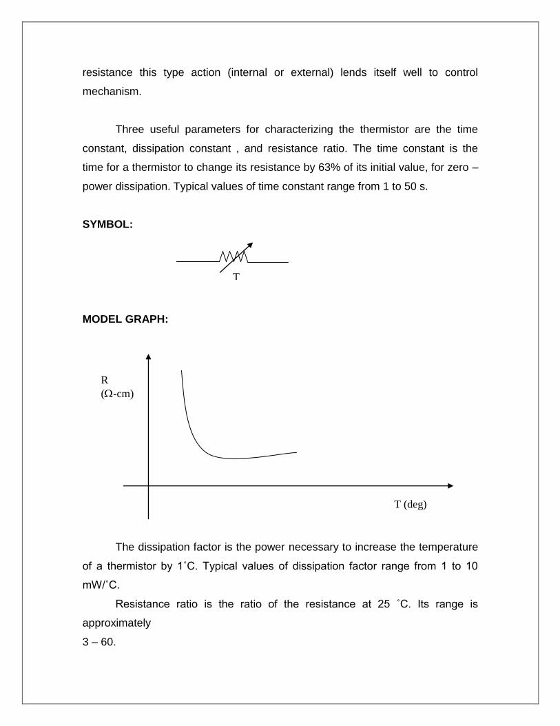
resistance this type action (internal or external) lends itself well to control
mechanism.
Three useful parameters for characterizing the thermistor are the time
constant, dissipation constant , and resistance ratio. The time constant is the
time for a thermistor to change its resistance by 63% of its initial value, for zero –
power dissipation. Typical values of time constant range from 1 to 50 s.
SYMBOL:
MODEL GRAPH:
The dissipation factor is the power necessary to increase the temperature
of a thermistor by 1˚C. Typical values of dissipation factor range from 1 to 10
mW/˚C.
Resistance ratio is the ratio of the resistance at 25 ˚C. Its range is
approximately
3 – 60.
R
(-cm)
T (deg)
T

Thermistors are used measure temperature, flow pressure, liquid level,
voltage or power level, vacuum, composition of gases and thermal conductivity
and also in compensation network.
RESULT:
Thus the Characteristics of thermistor was studied.
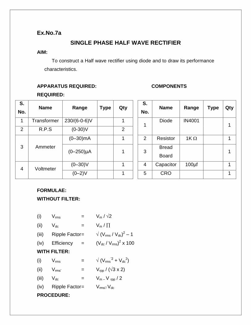
Ex.No.7a
SINGLE PHASE HALF WAVE RECTIFIER
AIM:
To construct a Half wave rectifier using diode and to draw its performance
characteristics.
APPARATUS REQUIRED: COMPONENTS
REQUIRED:
S.
No. Name Range Type Qty
S.
No. Name Range Type Qty
1 Transformer 230/(6-0-6)V 1 1
Diode IN4001 1
2 R.P.S (0-30)V 2
3 Ammeter
(0–30)mA 1 2 Resistor 1K 1
(0–250)µA 1 3 Bread
Board
1
4 Voltmeter (0–30)V 1 4 Capacitor 100µf 1
(0–2)V 1 5 CRO 1
FORMULAE:
WITHOUT FILTER:
(i) Vrms = Vm / 2
(ii) Vdc = Vm /
(iii) Ripple Factor = (Vrms / Vdc)2 – 1
(iv) Efficiency = (Vdc / Vrms)2 x 100
WITH FILTER:
(i) Vrms = (Vrms’2 + Vdc
2)
(ii) Vrms’ = Vrpp / (3 x 2)
(iii) Vdc = Vm – V rpp / 2
(iv) Ripple Factor = Vrms’/ Vdc
PROCEDURE:
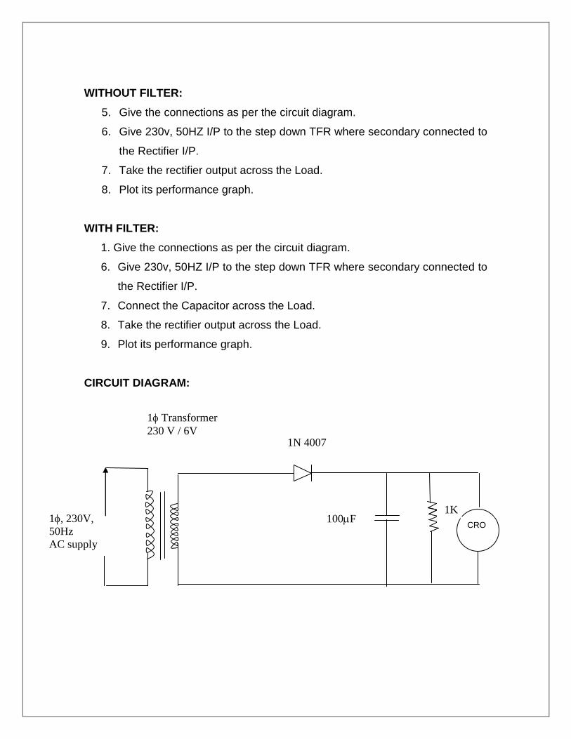
WITHOUT FILTER:
5. Give the connections as per the circuit diagram.
6. Give 230v, 50HZ I/P to the step down TFR where secondary connected to
the Rectifier I/P.
7. Take the rectifier output across the Load.
8. Plot its performance graph.
WITH FILTER:
1. Give the connections as per the circuit diagram.
6. Give 230v, 50HZ I/P to the step down TFR where secondary connected to
the Rectifier I/P.
7. Connect the Capacitor across the Load.
8. Take the rectifier output across the Load.
9. Plot its performance graph.
CIRCUIT DIAGRAM:
1 Transformer
230 V / 6V 1N 4007
1K 100F 1, 230V,
50Hz
AC supply
CRO

TABULAR COLUMN:
WITHOUT FILTER:
Vm Vrms Vdc Ripple factor Efficiency
WITH FILTER:
Vrms Vrpp Vdc Ripple factor Efficiency
MODEL GRAPH:
RESULT:
Thus the performance characteristics of 1 Half wave rectifier was obtained.
Ex.No.7b
Vin
(Volts)
t (ms)
Vo
(Volts)
t (ms)
t (ms)
Vo
(Volts)
Without Filter
With Filter

SINGLE PHASE FULL WAVE RECTIFIER
AIM:
To construct a Full wave rectifier using diode and to draw its performance
characteristics.
APPARATUS REQUIRED: COMPONENTS
REQUIRED:
S.
No. Name Range Type Qty
S.
No. Name Range Type Qty
1 Transformer 230/(6-0-6)V 1 1
Diode IN4001 2
2 R.P.S (0-30)V 2
3 Ammeter
(0–30)mA 1 2 Resistor 1K 1
(0–250)µA 1 3 Bread
Board
1
4 Voltmeter (0–30)V 1 4 Capacitor 100µf 1
(0–2)V 1 5 CRO 1
FORMULAE:
WITHOUT FILTER:
(i) Vrms = Vm / 2
(ii) Vdc = 2Vm /
(iii) Ripple Factor = (Vrms / Vdc)2 – 1
(iv) Efficiency = (Vdc / Vrms)2 x 100
WITH FILTER:
(i) Vrms = Vrpp /(2* 3)
(ii) Vdc = Vm – V rpp
(iv) Ripple Factor = Vrms’/ Vdc
PROCEDURE:
WITHOUT FILTER:
5. Give the connections as per the circuit diagram.
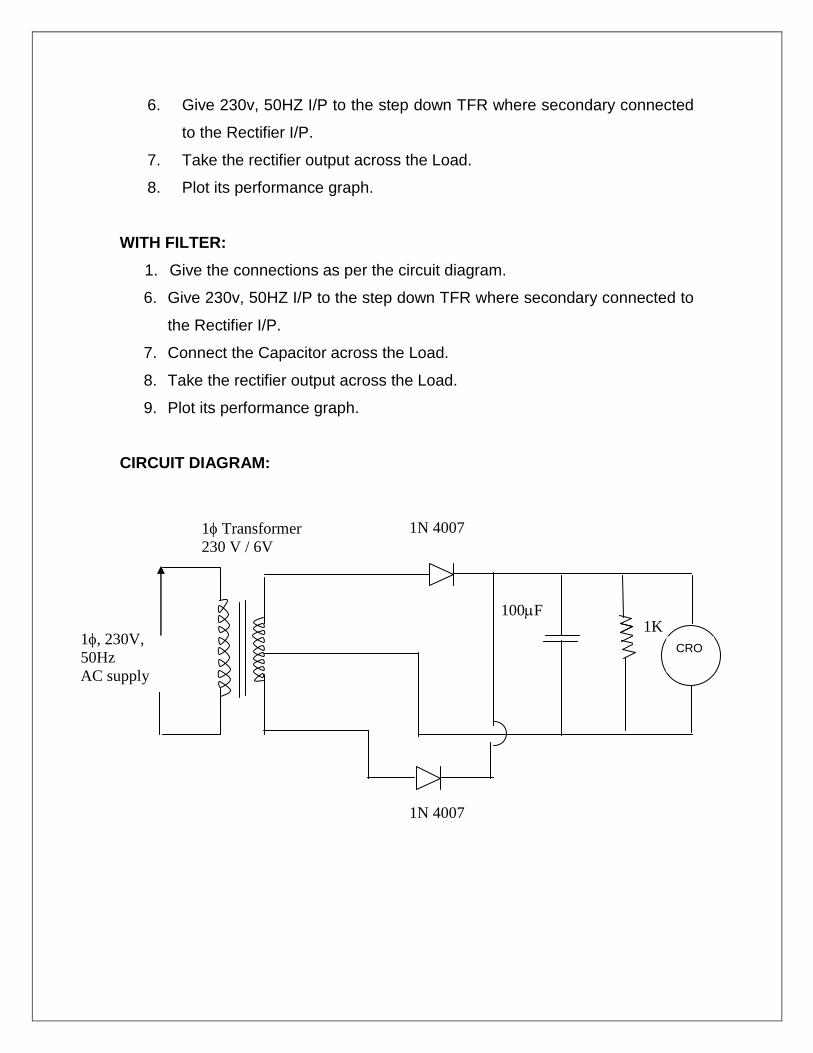
6. Give 230v, 50HZ I/P to the step down TFR where secondary connected
to the Rectifier I/P.
7. Take the rectifier output across the Load.
8. Plot its performance graph.
WITH FILTER:
1. Give the connections as per the circuit diagram.
6. Give 230v, 50HZ I/P to the step down TFR where secondary connected to
the Rectifier I/P.
7. Connect the Capacitor across the Load.
8. Take the rectifier output across the Load.
9. Plot its performance graph.
CIRCUIT DIAGRAM:
1N 4007
1K 100F
1, 230V,
50Hz
AC supply
CRO
1N 4007
1 Transformer
230 V / 6V

TABULAR COLUMN:
WITHOUT FILTER:
Vm Vrms Vdc Ripple factor Efficiency
WITH FILTER:
Vrms Vrpp Vdc Ripple factor Efficiency
MODEL GRAPH :
RESULT: Thus the performance characteristics of 1 Full wave rectifier were
obtained.
Ex.No.8
Vin
(Volts)
t (ms)
Vo
(Volts)
t (ms)
t (ms)
Vo
(Volts)
Without Filter
With Filter

DIFFERENTIAL AMPLIFIER
AIM:
To construct a Differential amplifier in Common mode & Differential mode
configuration and to find common mode rejection ratio.
APPARATUS REQUIRED: COMPONENTS REQUIRED:
Apparatus Range Qty
1 RPS (0-30)V 1
2 CRO 1
3 Signal
Generator 1
4 DCB 2
5 DRB 2
THEORY:
The Differential amplifier circuit is an extremely popular connection used in
IC units. The circuit has separate inputs , two separate outputs and emitters are
connected together. If the same input is applied to both inputs, the operation is
called common mode. In double ended operation two input signals are applied ,
the difference of the inputs resulting in outputs from both collectors due to the
difference of the signals applied to both the inputs. The main feature of the
differential amplifier is the very large gain when opposite signals are applied to
inputs as compared to small signal resulting from common input. The ratio of this
difference gain to the common gain is called common mode rejection ratio.
CIRCUIT DIAGRAM:
DIFFERENTIAL MODE:
S.No Item Type Range Qty
1 Transistor BC107 1
2 Capacitor 470F 1
3 Resistor 3.9KΩ
3.3KΩ
1
1
4 Bread board 1
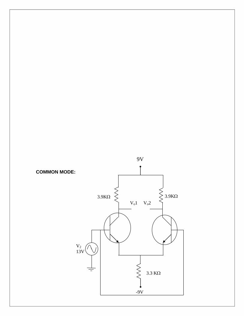
COMMON MODE:
9V
3.3 K
3.9K
Vo1 Vo2
V2
13V
3.9K
-9V

PROCEDURE:
DIFFERENTIAL MODE:
5. Connect the circuit as per the circuit diagram.
6. Set V1 = 50mv and V2 =55mv using the signal generator.
7. Find the corresponding output voltages across V01 & V02 using CRO
8. Calculate common mode rejection ratio using the given formula.
COMMON MODE:
5. Connect the circuit as per the circuit diagram.
6. Set V1 = 50mv using the signal generator.
7. Find the output voltage across Vo using multimeter.
8. Calculte common mode rejection ratio using the given formula.
CALCULATION:
Common mode rejection ratio(CMRR) = Ad / Ac
Ad = Differential mode gain
Ac = Common mode gain
Where Ad = Vo /Vd
Vo = Output voltage measured across CRO
Vd = V 1 – V2 , V 1 , V2 – input voltage applied.
Ac = Vo /Vc
Vc = (V 1 + V2 )/2
DIFFERENTIAL MODE:
V1 =
V2 =
Output voltage =
Vd= V1-V2 =
Ad=Vo/Vd =
RESULT: Thus the differential amplifier was constructed in common mode
and Differential mode configuration. Further common mode rejection ratio was
found
Exp. No: 12
COMMON MODE:
Input voltage =
Output voltage =
V1=V2 =
Vc=(V1+V2)/2 =

PASSIVE FILTERS
Aim:
To attenuate unwanted frequency components from input signal by using resistor
and capacitor.
Apparatus required:
S.No Name of the apparatus Range Type Quantity
1. Signal Generator 01
2. Resistor 01
3. Capacitor Ceramic 01
4. CRO 01
5. Breadboard 01
Theory:
A filter is an AC circuit that separates some frequencies from other in
within mixed – frequency signals. Audio equalizers and crossover networks are
two well-known applications of filter circuits. A Bode plot is a graph plotting
waveform amplitude or phase on one axis and frequency on the other.
A low-pass filter allows for easy passage of low-frequency signals from
source to load, and difficult passage of high-frequency signals. Capacitor low-pass
filters insert a resistor in series and a capacitor in parallel with the load as shown
in the circuit diagram. The former filter design tries to “block” the unwanted
frequency signal while the latter tries to short it out.
The cutoff frequency for a low-pass filter is that frequency at which the
output (load) voltage equals 70.7% of the input (Source) voltage. Above the cutoff
frequency, the output voltage is lower than 70.7% of the input, and vice-versa. See
the circuit diagram
1
Fcutoff = ----------
2RC
A high-pass filter allows for easy passage of high-frequency signals from source to
load, and difficult passage of low-frequency signals. Capacitor high-pass filters
insert a capacitor in series with the load as shown in the circuit diagram. The
former filter design tries to “brick” the unwanted frequency signal while the latter
tries to short it out.
The cutoff frequency for a high-pass filter is that frequency at which the
output (load) voltage equals 70.7% of the input (source) voltage. Above the cutoff
frequency, the output voltage is greater than 70.7% of the input, and vice-versa.
1
Fcutoff = ----------
2RC
A band – pass filter works to screen out frequencies that are too low or too
high, giving easy passage only to frequencies within a certain range. Stacking a
low-pass filter on the end of a high-pass filter, or vice-versa can make band-pass
filters. Refer the circuit diagrams
Fig. 7.6
“Attenuate” means to reduce or diminish in amplitude. When you
turn down the volume control on your stereo, you are “attenuating” the signal
being sent to the speakers.
A band-stop filter works to screen out frequencies that are within a certain
range, giving easy passage only to frequencies outside of that range. Also known
as band-elimination, band-reject, or notch filters.
Placing a low-pass filter in parallel with a high-pass filter can make band-
stop filters. Commonly, both the low-pass and high-pass filter sections are of the
Signal
input
Low-pass filter High-pass filter Signal
output Blocks frequencies
that are too high
Blocks frequencies
that are too low
Signal
Input
Low-pass filter
High-pass filter
Signal
Output
“T” configuration giving the name “Twin-T” to the band-stop combination. Refer
the fig.7.7, 7.8a and 7.8b.
Passes low frequencies
Passes high frequencies
Fig. 7.8a
The frequency of maximum attenuation is called the notch
frequency.
Procedure:
7. Give the connections as per circuit diagrams.
8. Switch on the main.
9. Change the frequency from minimum and find the output
voltage by using CRO.
10. Draw the graph.
11. Verify the cut off frequency.
12. Switch off the main.
Result:
Thus we analyze passive filter and various waveforms are noted
Exp. No : 10
STUDY OF CRO AND
POWER FACTOR MEASUREMENT USING CRO
Aim:
To study cathode Ray Oscilloscope (CRO) and measurement of power factor using
CRO.

Apparatus required:
S.No Name of the apparatus Range Type Quantity
1. Resistance Box 1
2. Capacitance Box 1
3. Inductance Box 1
4. Function Generator 1
5. Bread board 1
Theory:
The cathode ray oscilloscope is the most versatile measuring instrument
available. We can measure following parameters using the CRO:
5. AC or DC voltage.
6. Time (t=1/f).
7. Phase relationship
8. Waveform calculation: Rise time; fall time; on time; off-time
Distortion, etc.
We can also measure non-electrical physical quantities like pressure, strain,
temperature, acceleration, etc., by converting into electrical quantities using
a transducer.
Major blocks:
7. Cathode ray tube (CRT)
8. Vertical amplifier
9. Horizontal amplifier
10. Sweep generator
11. Trigger circuit
12. Associated power supply.

6. The cathode ray tube is the heart of CRO. The CRT is enclosed in an
evacuated glass envelope to permit the electron beam to traverse in the
tube easily. The main functional units of CRO are as follows.
Electron gun assembly
Deflection plate unit
Screen.
7. Vertical Amplifier is the main factor in determining the bandwidth and
sensitivity of an oscilloscope. Vertical sensitivity is a measure of how
much the electron beam will be deflected for a specified input signal.
On the front panel of the oscilloscope, one can see a knob attached to a
rotary switch labeled volts/division. The rotary switch is electrically
connected to the input attenuation network. The setting of the rotary
switch indicates what amplitude signal is required to deflect the beam
vertically by one division.
8. Horizontal amplifier Under normal mode of operation, the horizontal
amplifier will amplify the sweep generator input. When the CRO is
being used in the X-Y mode, the horizontal amplifier will amplify the
signal applied to the horizontal input terminal. Although the vertical
amplifier mush be able to faithfully reproduce low-amplitude and high
frequency signal with fast rise-time, the horizontal amplifier is only
required to provide a faithful reproduction of the sweep signal which
has a relatively high amplitude and slow rise time.
9. Sweep generator and Trigger circuit These two units form the Signal
Synchronization unit of the CRO.
10. Associated Power Supply: The input signal may come from an
external source when the trigger selector switch is set to EXT or from
low amplitude AC voltage at line frequency when the switch is set to
LINE or from the vertical amplifier when the switch is set to INT. When
set for INT (internal triggering), the trigger circuit receives its inputs
from the vertical amplifier.
Major Blocks in a Practical CRO
A CRO consists of a cathode ray tube (CRT) and additional control knobs.
The main parts of a CRT are:
4. Electron gun assembly.
5. Deflection plate assembly.
6. Fluorescent screen.
Electron Gun Assembly: The electron gun assembly produces a sharp beam of
electrons, which are accelerated to high velocity. This focused beam of electrons
strike the fluorescent screen with sufficient energy to cause a luminous spot on the
screen.
Deflection plate assembly: This part consists of two plates in which one pair of
plates is placed horizontally and other of plates is placed vertically. The signal
under test is applied to vertical deflecting plates. The horizontal deflection plates
are connected to a built-in ramp generator, which moves the luminous spot
periodically in a horizontal direction from left to right over the screen. These two
deflection plates give stationary appearance to the waveform on the screen. CRO
operates on voltage. Since the deflection of the electron beam is directly
proportional to the deflecting voltage, the CRT may be used as a linear measuring
device. The voltage being measured is applied to the vertical plates through an
iterative network, whose propagation time corresponds to the velocity of electrons,
thereby synchronizing the voltage applied to the vertical plate with the velocity of
the beam.
Synchronization of input signal: The sweep generator produces a saw tooth
waveform, which is used to synchronize the applied voltage to obtain a stationary-
applied signal. This requires that the time base be operated at a submultiples
frequency of the signal under measurement. If synchronization is not done, the
pattern is not stationary, but appears to drift across the screen in a random fashion.
Internal synchronization This trigger is obtained from the time base generator to
synchronize the signal.
External synchronization An external trigger source can also be used to
synchronize the signal being measured.
Auto Triggering Mode The time base used in this case in a self-oscillating
condition, i.e., it gives an output even in the absence of any Y-input. The
advantage of this mode is that the beam is visible on the screen under all
conditions, including the zero input. When the input exceeds a certain magnitude
then the internal free running oscillator locks on to the frequency.
Precautions:
3. The ammeter is connected using thick wires.
4. While reversing ammeter polarity, see to it that the capacitor is not
discharged.
Observation:
Sl.No Time Voltage Current
Unit (Sec) (Volts) (Amps)
Result: Thus we study about CRO & to measure p.f
CLASS : II YEAR/ III SEMSESTER
SUBJECT CODE : 131351
SUBJECT : ELECTRON DEVICES AND CIRCUITS LAB
BATCH : B1
STAFF IN-CHARGE: Mrs. A. ALICE HEPZIBAH
DESIGNATION : ASSISTANT PROFESSOR
STAFF CODE : EE10
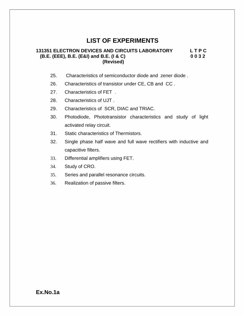
LIST OF EXPERIMENTS
131351 ELECTRON DEVICES AND CIRCUITS LABORATORY L T P C (B.E. (EEE), B.E. (E&I) and B.E. (I & C) 0 0 3 2 (Revised)
25. Characteristics of semiconductor diode and zener diode .
26. Characteristics of transistor under CE, CB and CC .
27. Characteristics of FET .
28. Characteristics of UJT .
29. Characteristics of SCR, DIAC and TRIAC.
30. Photodiode, Phototransistor characteristics and study of light
activated relay circuit.
31. Static characteristics of Thermistors.
32. Single phase half wave and full wave rectifiers with inductive and
capacitive filters.
33. Differential amplifiers using FET.
34. Study of CRO.
35. Series and parallel resonance circuits.
36. Realization of passive filters.
Ex.No.1a

CHARACTERISTICS OF PN JUNCTION DIODE
AIM:
To study the PN junction diode characteristics under Forward & Reverse
bias conditions.
APPARATUS REQUIRED: COMPONENTS REQUIRED:
S.No. Name Range Type Qty
S.No. Name Range Type Qty
1 R.P.S 1 Diode
2 Ammeter
2 Resistor
3 Bread
Board
3 Voltmeter 4 Wires
THEORY:
A PN junction diode is a two terminal junction device. It conducts only in
one direction (only on forward biasing).
FORWARD BIAS:
On forward biasing, initially no current flows due to barrier potential. As the
applied potential exceeds the barrier potential the charge carriers gain sufficient
energy to cross the potential barrier and hence enter the other region. The holes,
which are majority carriers in the P-region, become minority carriers on entering
the N-regions, and electrons, which are the majority carriers in the N-region,
become minority carriers on entering the P-region. This injection of Minority
carriers results in the current flow, opposite to the direction of electron
movement.

REVERSE BIAS:
On reverse biasing, the majority charge carriers are attracted towards the
terminals due to the applied potential resulting in the widening of the depletion
region. Since the charge carriers are pushed towards the terminals no current
flows in the device due to majority charge carriers. There will be some current in
the device due to the thermally generated minority carriers. The generation of
such carriers is independent of the applied potential and hence the current is
constant for all increasing reverse potential. This current is referred to as
Reverse Saturation Current (IO) and it increases with temperature. When the
applied reverse voltage is increased beyond the certain limit, it results in
breakdown. During breakdown, the diode current increases tremendously.
PROCEDURE:
FORWARD BIAS:
9. Connect the circuit as per the diagram.
10. Vary the applied voltage V in steps of 0.1V.
11. Note down the corresponding Ammeter readings I.
12. Plot a graph between V & I
OBSERVATIONS
7. Find the d.c (static) resistance = V/I.
8. Find the a.c (dynamic) resistance r = V / I (r = V/I) = 12
12
II
VV
.
9. Find the forward voltage drop = [Hint: it is equal to 0.7 for Si and 0.3 for
Ge]
REVERSE BIAS:
11. Connect the circuit as per the diagram.
12. Vary the applied voltage V in steps of 1.0V.
13. Note down the corresponding Ammeter readings I.
14. Plot a graph between V & I
15. Find the dynamic resistance r = V / I.

(0-100)mA, MC
+ -
+
+
-
+
(0-15)V, MC +
-
+
(0-10)V
RPS
(0-500)µA,MC
+ -
+
+
-
+
(0-30)V, MC +
-
+
(0-30)V
RPS
FORMULA FOR REVERSE SATURATION CURRENT (IO):
Io = I/[exp(V/VT)]-1
Where VT is the voltage equivalent of Temperature = kT/q
-k is Boltzmann’s constant, q is the charge of the electron and T is the
temperature in degrees Kelvin.
=1 for Silicon and 2 for Germanium
CIRCUIT DIAGRAM:
FORWARD BIAS:
REVERSE BIAS:
Specification for 1N4001: Silicon Diode
Peak Inverse Voltage: 50V
470 a
a
a
a
a
A
A
A
470 a
a
a
a
a
A
A
A

Idc = 1A.
Maximum forward voltage drop at 1 Amp is 1.1 volts
Maximum reverse current @50 volts is 5A
TABULAR COLUMN:
FORWARD BIAS: REVERSE BIAS:
MODEL GRAPH
If (mA)
I2
Vb I1
( Volts) V1 V2 Vf
(Volts)
Ir (A)
RESULT:
Forward and Reverse bias characteristics of the PN junction diode and the
dynamic resistance under
S.No. VOLTAGE
(In Volts)
CURRENT
(In mA)
S..No. VOLTAGE
(In Volts)
CURRENT
(In A)

i) Forward bias = ---------------------
ii) Reverse bias = ----------------------.
iii) Reverse Saturation Current = ----------------.

Ex.No.1b
CHARACTERISTICS OF ZENER DIODE
AIM:
To determine the breakdown voltage of a given zener diode.
APPARATUS REQUIRED: COMPONENTS REQUIRED:
S.No. Name Range Type Qty
S.No. Name Range Type Qty
1 R.P.S 1 zener
diode
2 Ammeter
2 Resistor
3 Bread
Board
3 Voltmeter 4 Wires
THEORY:
A properly doped crystal diode, which has a sharp breakdown voltage, is known
as zener diode.
FORWARD BIAS:
On forward biasing, initially no current flows due to barrier potential. As the
applied potential increases, it exceeds the barrier potential at one value and the
charge carriers gain sufficient energy to cross the potential barrier and enter the
other region. the holes ,which are majority carriers in p-region, become minority
carriers on entering the N-regions and electrons, which are the majority carriers
in the N-regions become minority carriers on entering the P-region. This injection
of minority carriers results current, opposite to the direction of electron
movement.
REVERSE BIAS:

When the reverse bias is applied due to majority carriers small amount of
current (ie) reverse saturation current flows across the junction. As the reverse
bias is increased to breakdown voltage, sudden rise in current takes place due to
zener effect.
ZENER EFFECT:
Normally, PN junction of Zener Diode is heavily doped. Due to heavy
doping the depletion layer will be narrow. When the reverse bias is increased the
potential across the depletion layer is more. This exerts a force on the electrons
in the outermost shell. Because of this force the electrons are pulled away from
the parent nuclei and become free electrons. This ionization, which occurs due to
electrostatic force of attraction, is known as Zener effect. It results in large
number of free carriers, which in turn increases the reverse saturation current
PROCEDURE:
FORWARD BIAS:
1. Connect the circuit as per the circuit diagram.
2. Vary the power supply in such a way that the readings are taken in steps
of 0.1V in the voltmeter till the needle of power supply shows 30V.
3. Note down the corresponding ammeter readings.
4. Plot the graph :V (vs) I.
5. Find the dynamic resistance r = V / I.
REVERSE BIAS:
13. Connect the circuit as per the diagram.
14. Vary the power supply in such a way that the readings are taken in steps
of 0.1V in the voltmeter till the needle of power supply shows 30V.
15. Note down the corresponding Ammeter readings I.
16. Plot a graph between V & I
17. Find the dynamic resistance r = V / I.
18. Find the reverse voltage Vr at Iz=20 mA.
CIRCUIT DIAGRAM:

(0-15) V
+ -
+
-
+
-
(0-10) V
(0-10) V, MC
+ -
+
-
+
-
(0-30) V
FORWARD BIAS:
REVERSE BIAS:
1K
a
a
a
a
a
A
A
A
a
a
a
a
a
A
A
A
470
aaaa
aAA
A
aaaa
aAA
A
a
a
a
a
a
A
A
A
(0-10)mA
1
K
a
a
a
a
a
A
A
A
a
a
a
a
a
A
A
A
1K
aaaa
aAA
A
aaaa
aAA
A
a
a
a
a
a
A
A
A
(0-500)μA, MC

ZENER DIODE:
If ( mA)
I2
VB I1
Vr V1 V2 Vf
(V) (V)
Ir (μA)
TABULAR COLUMN:
FORWARD BIAS: REVERSE BIAS:
RESULT:
Forward and Reverse bias characteristics of the zener diode was studied
and
Forward bias dynamic resistance = ---------------------
Reverse bias dynamic resistance = ----------------------
The reverse voltage at Iz =20 mA determined from the reverse
characteristics of the Zener diode is --------------------------.
S..No. VOLTAGE
(In Volts)
CURRENT
(In mA)
S.No. VOLTAGE
(In Volts)
CURRENT
(In A)
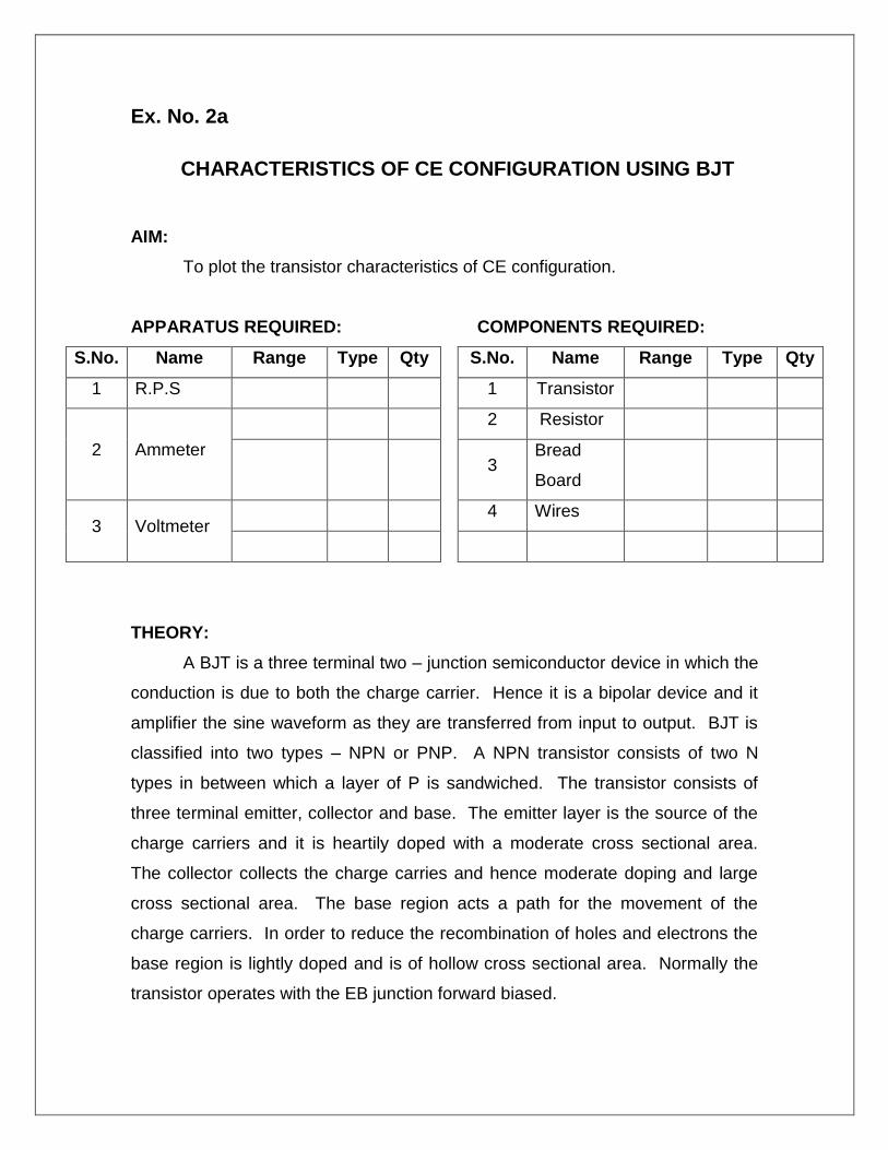
Ex. No. 2a
CHARACTERISTICS OF CE CONFIGURATION USING BJT
AIM:
To plot the transistor characteristics of CE configuration.
APPARATUS REQUIRED: COMPONENTS REQUIRED:
S.No. Name Range Type Qty
S.No. Name Range Type Qty
1 R.P.S 1 Transistor
2 Ammeter
2 Resistor
3 Bread
Board
3 Voltmeter 4 Wires
THEORY:
A BJT is a three terminal two – junction semiconductor device in which the
conduction is due to both the charge carrier. Hence it is a bipolar device and it
amplifier the sine waveform as they are transferred from input to output. BJT is
classified into two types – NPN or PNP. A NPN transistor consists of two N
types in between which a layer of P is sandwiched. The transistor consists of
three terminal emitter, collector and base. The emitter layer is the source of the
charge carriers and it is heartily doped with a moderate cross sectional area.
The collector collects the charge carries and hence moderate doping and large
cross sectional area. The base region acts a path for the movement of the
charge carriers. In order to reduce the recombination of holes and electrons the
base region is lightly doped and is of hollow cross sectional area. Normally the
transistor operates with the EB junction forward biased.

Bottom View BC107 Specification: BC107/50V/0.1A,0.3W,300MHz
(0 – 30)mA 1 K
In transistor, the current is same in both junctions, which indicates that
there is a transfer of resistance between the two junctions. One to this fact the
transistor is known as transfer resistance of transistor.
PROCEDURE:
INPUT CHARACTERISTICS:
7. Connect the circuit as per the circuit diagram.
8. Set VCE, vary VBE in regular interval of steps and note down the
corresponding IB reading. Repeat the above procedure for different values of
VCE.
9. Plot the graph: VBE Vs IB for a constant VCE.
OUTPUT CHARACTERISTICS:
7. Connect the circuit as per the circuit diagram.
8. Set IB, Vary VCE in regular interval of steps and note down the
corresponding IC reading. Repeat the above procedure for different
values of IB.
9. Plot the graph: VCE Vs IC for a constant IB.
PIN DIAGRAM:
B
E C
CIRCUIT DIAGRAM:
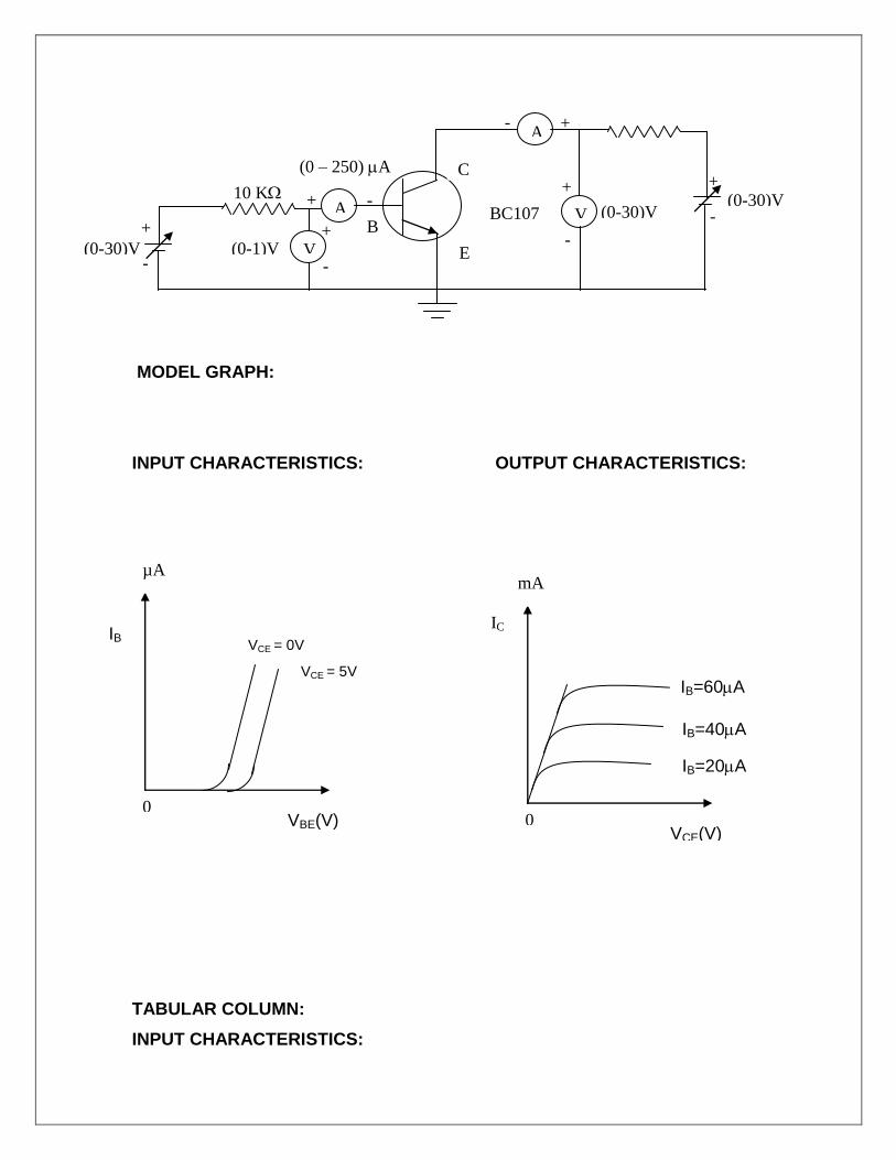
(0 – 250) A
10 K
- +
BC107
10 KΩ
+
-
+
+
-
+
(0-30)V
+
-
+
+
-
+
+ -
+
(0-30)V
(0-30)V
(0-1)V
MODEL GRAPH:
INPUT CHARACTERISTICS: OUTPUT CHARACTERISTICS:
TABULAR COLUMN:
INPUT CHARACTERISTICS:
A
A
V
V
C
E
C
B
C
VCE = 0V
VCE = 5V
IB
µA mA
VBE(V) VCE(V)
0 0
IB=60A
IB=40A
IB=20A
IC
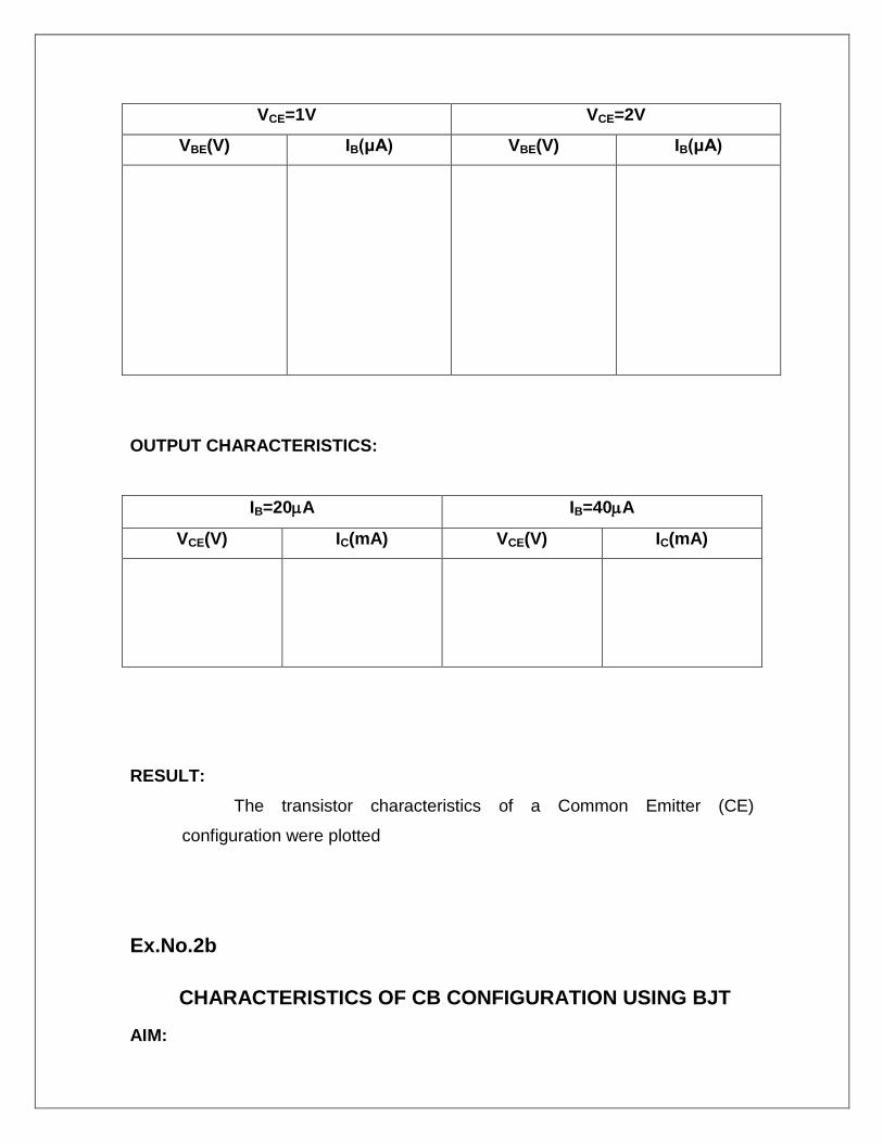
VCE=1V VCE=2V
VBE(V) IB(μA) VBE(V) IB(μA)
OUTPUT CHARACTERISTICS:
IB=20A IB=40A
VCE(V) IC(mA) VCE(V) IC(mA)
RESULT:
The transistor characteristics of a Common Emitter (CE)
configuration were plotted
Ex.No.2b
CHARACTERISTICS OF CB CONFIGURATION USING BJT
AIM:

To plot the transistor characteristics of CB configuration.
APPARATUS REQUIRED: COMPONENTS REQUIRED:
S.No. Name Range Type Qty
S.No. Name Range Type Qty
1 R.P.S (0-30)V 2 1 Transistor BC 107 1
2 Ammeter
(0–10)mA 1 2 Resistor 10k
1K
1
(0–1)A 1 3 Bread
Board
1
3 Voltmeter (0–30)V 1 4 Wires
(0–2)V 1
THEORY:
In this configuration the base is made common to both the input and out.
The emitter is given the input and the output is taken across the collector. The
current gain of this configuration is less than unity. The voltage gain of CB
configuration is high. Due to the high voltage gain, the power gain is also high. In
CB configuration, Base is common to both input and output. In CB configuration
the input characteristics relate IE and VEB for a constant VCB. Initially let VCB = 0
then the input junction is equivalent to a forward biased diode and the
characteristics resembles that of a diode. Where VCB = +VI (volts) due to early
effect IE increases and so the characteristics shifts to the left. The output
characteristics relate IC and VCB for a constant IE. Initially IC increases and then it
levels for a value IC = IE. When IE is increased IC also increases proportionality.
Though increase in VCB causes an increase in , since is a fraction, it is
negligible and so IC remains a constant for all values of VCB once it levels off.
PIN DIAGRAM:
B
Bottom View BC107 Specification: BC107/50V/0.1A,0.3W,300MHz

(0-30)V
(0-1)mA
+ -
+
(0-30)mA
+ -
+
+
-
+
+
-
+
+
-
+
(0-2)V (0-30)V (0-30)V
E C
CIRCUIT DIAGRAM:
-
PROCEDURE:
INPUT CHARACTERISTICS:
It is the curve between emitter current IE and emitter-base voltage VBE at
constant collector-base voltage VCB.
9. Connect the circuit as per the circuit diagram.
10. Set VCE=5V, vary VBE in steps of 0.1V and note down the corresponding
IB. Repeat the above procedure for 10V, 15V.
11. Plot the graph VBE Vs IB for a constant VCE.
12. Find the h parameters.
OUTPUT CHARACTERISTICS:
It is the curve between collector current IC and collector-base voltage VCB at
constant emitter current IE.
9. Connect the circuit as per the circuit diagram.
10. Set IB=20A, vary VCE in steps of 1V and note down the corresponding IC.
Repeat the above procedure for 40A, 80A, etc.
11. Plot the graph VCE Vs IC for a constant IB.
12. Find the h parameters
a
a
a
a
a
A
A
A
10 K
a
a
a
a
a
A
A
A
a
a
a
a
a
A
A
A
a
a
a
a
a
A
A
A
a
a
a
a
a
A
A
A
a
a
a
a
a
A
A
A
1K
VEB
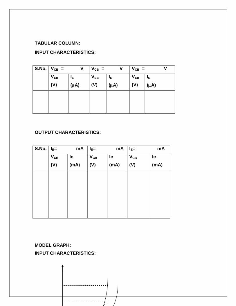
TABULAR COLUMN:
INPUT CHARACTERISTICS:
S.No. VCB = V VCB = V VCB = V
VEB
(V)
IE
(A)
VEB
(V)
IE
(A)
VEB
(V)
IE
(A)
OUTPUT CHARACTERISTICS:
S.No. IE= mA IE= mA IE= mA
VCB
(V)
Ic
(mA)
VCB
(V)
Ic
(mA)
VCB
(V)
Ic
(mA)
MODEL GRAPH:
INPUT CHARACTERISTICS:
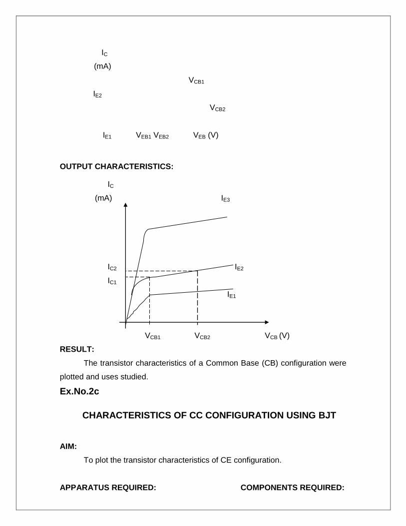
IC
(mA)
VCB1
IE2
VCB2
IE1 VEB1 VEB2 VEB (V)
OUTPUT CHARACTERISTICS:
IC
(mA) IE3
IC2 IE2
IC1
IE1
VCB1 VCB2 VCB (V)
RESULT:
The transistor characteristics of a Common Base (CB) configuration were
plotted and uses studied.
Ex.No.2c
CHARACTERISTICS OF CC CONFIGURATION USING BJT
AIM:
To plot the transistor characteristics of CE configuration.
APPARATUS REQUIRED: COMPONENTS REQUIRED:

Bottom View BC107 Specification: BC107/50V/0.1A,0.3W,300MHz
S.No. Name Range Type Qty
S.No. Name Range Type Qty
1 R.P.S (0-30)V 2 1 Transistor BC 107 1
2 Ammeter
(0–30)mA 1 2 Resistor 1k 2
(0–250)µA 1 3 Bread
Board
1
3 Voltmeter (0–30)V 1 4 Wires
(0–5)V 1
THEORY:
A BJT is a three terminal two – junction semiconductor device in which the
conduction is due to both the charge carrier. Hence it is a bipolar device and it
amplifier the sine waveform as they are transferred from input to output. BJT is
classified into two types – NPN or PNP. A NPN transistor consists of two N
types in between which a layer of P is sandwiched. The transistor consists of
three terminal emitter, collector and base. The emitter layer is the source of the
charge carriers and it is heartily doped with a moderate cross sectional area.
The collector collects the charge carries and hence moderate doping and large
cross sectional area. The base region acts a path for the movement of the
charge carriers. In order to reduce the recombination of holes and electrons the
base region is lightly doped and is of hollow cross sectional area. Normally the
transistor operates with the EB junction forward biased.
In transistor, the current is same in both junctions, which indicates that
there is a transfer of resistance between the two junctions. One to this fact the
transistor is known as transfer resistance of transistor.
PIN DIAGRAM:
B
E C

+
-
+
-
+
+ -
+
+ +
-
+
+
+ -
+
(0-30)mA
(0-250)µA
CIRCUIT DIAGRAM:
PROCEDURE:
INPUT CHARECTERISTICS:
7. Connect the circuit as per the circuit diagram.
8. Set VCE, vary VBE in regular interval of steps and note down the
corresponding IB reading. Repeat the above procedure for different values
of VCE.
9. Plot the graph: VBC Vs IB for a constant VCE.
OUTPUT CHARECTERISTICS:
7. Connect the circuit as per the circuit diagram.
8. Set IB, Vary VCE in regular interval of steps and note down the
corresponding IC reading. Repeat the above procedure for different
values of IB.
9. Plot the graph: VCE Vs IC for a constant IB.
MODEL GRAPH:
INPUT CHARACTERISTICS: OUTPUT CHARACTERISTICS:
A
A V
V
1 K
+
-
+
(0-30)V (0-30)V
(0-30)V (0-30)V
1 K
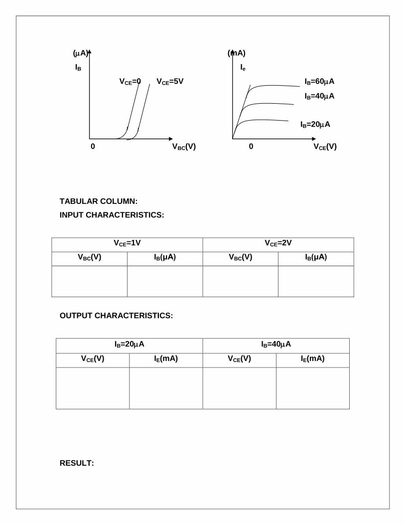
(A) (mA)
IB Ie
VCE=0 VCE=5V IB=60A
IB=40A
IB=20A
0 VBC(V) 0 VCE(V)
TABULAR COLUMN:
INPUT CHARACTERISTICS:
VCE=1V VCE=2V
VBC(V) IB(μA) VBC(V) IB(μA)
OUTPUT CHARACTERISTICS:
IB=20A IB=40A
VCE(V) IE(mA) VCE(V) IE(mA)
RESULT:

The transistor characteristics of a Common Emitter (CC) configuration
were plotted.
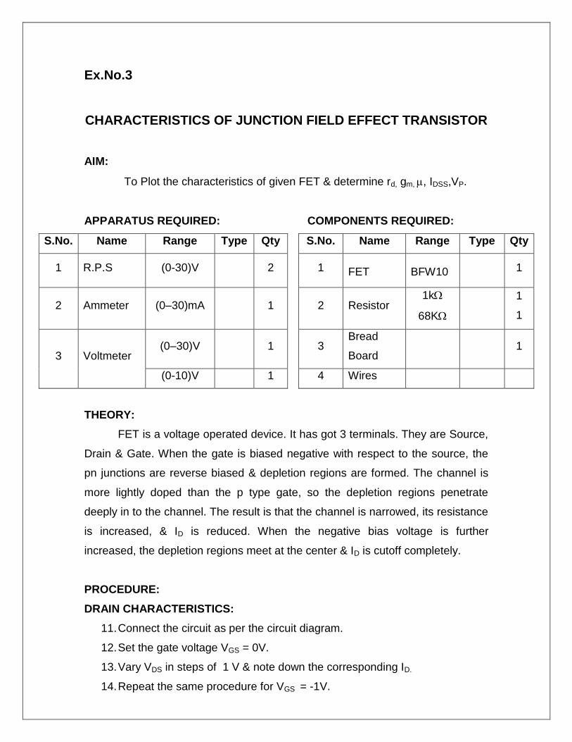
Ex.No.3
CHARACTERISTICS OF JUNCTION FIELD EFFECT TRANSISTOR
AIM:
To Plot the characteristics of given FET & determine rd, gm, , IDSS,VP.
APPARATUS REQUIRED: COMPONENTS REQUIRED:
S.No. Name Range Type Qty
S.No. Name Range Type Qty
1 R.P.S (0-30)V 2 1 FET BFW10 1
2 Ammeter (0–30)mA 1 2 Resistor 1k
68K
1
1
3 Voltmeter (0–30)V 1 3
Bread
Board
1
(0-10)V 1 4 Wires
THEORY:
FET is a voltage operated device. It has got 3 terminals. They are Source,
Drain & Gate. When the gate is biased negative with respect to the source, the
pn junctions are reverse biased & depletion regions are formed. The channel is
more lightly doped than the p type gate, so the depletion regions penetrate
deeply in to the channel. The result is that the channel is narrowed, its resistance
is increased, & ID is reduced. When the negative bias voltage is further
increased, the depletion regions meet at the center & ID is cutoff completely.
PROCEDURE:
DRAIN CHARACTERISTICS:
11. Connect the circuit as per the circuit diagram.
12. Set the gate voltage VGS = 0V.
13. Vary VDS in steps of 1 V & note down the corresponding ID.
14. Repeat the same procedure for VGS = -1V.
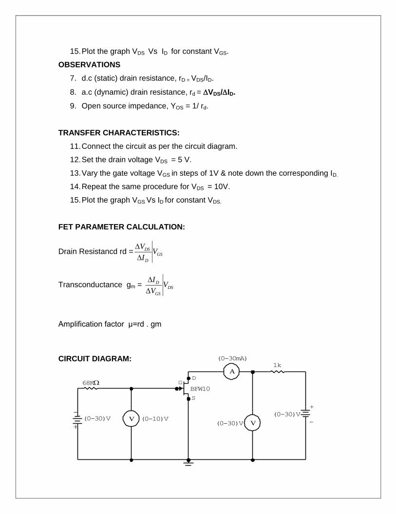
+ (0-30)V
68K
V
+
(0-30)V
(0-30)V
1k (0-30mA)
D G
S
BFW10
-
+ (0-10)V V
A
V
-
15. Plot the graph VDS Vs ID for constant VGS.
OBSERVATIONS
7. d.c (static) drain resistance, rD = VDS/ID.
8. a.c (dynamic) drain resistance, rd = VDS/ID.
9. Open source impedance, YOS = 1/ rd.
TRANSFER CHARACTERISTICS:
11. Connect the circuit as per the circuit diagram.
12. Set the drain voltage VDS = 5 V.
13. Vary the gate voltage VGS in steps of 1V & note down the corresponding ID.
14. Repeat the same procedure for VDS = 10V.
15. Plot the graph VGS Vs ID for constant VDS.
FET PARAMETER CALCULATION:
Drain Resistancd rd = GS
D
DS VI
V
Transconductance gm = DS
GS
D VV
I
Amplification factor μ=rd . gm
CIRCUIT DIAGRAM:

I D (
mA
)
PIN DIAGRAM:
BOTTOM VIEW OF BFW10:
SPECIFICATION:
Voltage : 30V, IDSS > 8mA.
MODEL GRAPH:
DRAIN CHARACTERISTICS:
TRANSFER CHARACTERISTICS:
ID(mA)
VDS =Const
VGS (V)
TABULAR COLUMN:
0
VGS = 0V
VGS = -1V
VGS = -2V
VGS = -3V
VDS (volts)

DRAIN CHARACTERISTICS:
VGS = 0V VGS = -1V
VDS (V) ID(mA) VDS (V) ID(mA)
TRANSFER CHARACTERISTICS:
RESULT:
Thus the Drain & Transfer characteristics of given FET is Plotted.
Rd =
gm =
=
IDSS =
Pinch off voltage VP =
VDS =5volts VDS = 10volts
VGS (V) ID(mA) VGS (V) ID(mA)

Ex.No.4
CHARACTERISTICS OF UNIJUNCTION TRANSISTOR
AIM:
To Plot the characteristics of UJT & determine it’s intrinsic standoff
Ratio.
APPARATUS REQUIRED: COMPONENTS REQUIRED:
S.
No. Name Range Type Qty
S.
No. Name Range Type Qty
1 R.P.S (0-30)V 2 1 UJT 2N2646 1
2 Ammeter (0–30)mA 1
2 Resistor 1K 2
3 Bread
Board
1
3 Voltmeter (0–30)V 1
(0–10)V 1
THEORY:
UJT(Double base diode) consists of a bar of lightly doped n-type silicon
with a small piece of heavily doped P type material joined to one side. It has got
three terminals. They are Emitter(E), Base1(B1),Base2(B2).Since the silicon bar
is lightly doped, it has a high resistance & can be represented as two resistors,
rB1 & rB2. When VB1B2 = 0, a small increase in VE forward biases the emitter
junction. The resultant plot of VE & I E is simply the characteristics of forward
biased diode with resistance. Increasing VEB1 reduces the emitter junction
reverse bias. When VEB1 = VrB1 there is no forward or reverse bias. & IE = 0.
Increasing VEB1 beyond this point begins to forward bias the emitter junction. At
the peak point, a small forward emitter current is flowing. This current is termed
as peak current( IP ). Until this point UJT is said to be operating in cutoff region.
When IE increases beyond peak current the device enters the negative
resistance region. In which the resistance rB1 falls rapidly & VE falls to the valley
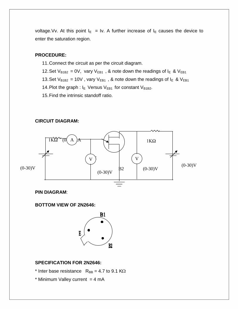
B2
E
voltage.Vv. At this point IE = Iv. A further increase of IE causes the device to
enter the saturation region.
PROCEDURE:
11. Connect the circuit as per the circuit diagram.
12. Set VB1B2 = 0V, vary VEB1 , & note down the readings of IE & VEB1
13. Set VB1B2 = 10V , vary VEB1 , & note down the readings of IE & VEB1
14. Plot the graph : IE Versus VEB1 for constant VB1B2.
15. Find the intrinsic standoff ratio.
CIRCUIT DIAGRAM:
PIN DIAGRAM:
BOTTOM VIEW OF 2N2646:
SPECIFICATION FOR 2N2646:
* Inter base resistance RBB = 4.7 to 9.1 K
* Minimum Valley current = 4 mA
B2
(0-30)V (0-30)V
(0-30)V
1KΩ 1KΩ
(0-30)V
(0-30)mA
V V
A

* Maximun Peak point emitter current 5 A
*Maximum emitter reverse current 12 A.
FORMULA FOR INTRINSIC STANDOFF RATIO:
= VP - VD/ VB1B2., where VD = 0.7V.
MODEL GRAPH:
Peak point
VP
IP
Negative resistance region
VEB1(V)
Valley point VB1B2 = V
VB1B2 = 0V
IV IE (mA)
TABULAR COLUMN:
VB1B2 = 0V VB1B2 = 10V
VEB1 (V) IE (mA) VEB1 (V) IE (mA)

PROCEDURE:
9. Give the circuit connections as per the circuit diagram.
10. The dc input voltage is set to 20 V in RPS.
11. The output sweep waveform is measured using CRO.
12. The graph of output sweep waveform is plotted
RESULT:
1. Thus the characteristics of given UJT was Plotted & its intrinsic standoff
Ratio = ----.

Ex.No.5
CHARACTERISTICS OF PHOTO-DIODE AND
PHOTOTRANSISTOR
AIM:
1. To study the characteristics of a photo-diode.
2. To study the characteristics of phototransistor.
APPARATUS REQUIRED: COMPONENTS REQUIRED:
S.
No. Name Range Type Qty
S.
No. Name Range Type Qty
1 R.P.S (0-30)V 1 1 Photo
diode 1
2 Ammeter (0–30)mA 1
2 Resistor 1K 2
3 Bread
Board 1
3 Voltmeter (0–30)V 1 4 Photo
transistor 1
THEORY:
PHOTODIODE:
A photo diode is a two terminal pn junction device, which operates on
reverse bias. On reverse biasing a pn junction diode, there results a constant
current due to minority charge carriers known as reverse saturation current.
Increasing the thermally generated minority carriers by applying external energy,
i.e., either heat or light energy at the junction can increase this current. When we
apply light energy as an external source, it results in a photo diode that is usually
placed in a glass package so that light can reach the junction. Initially when no
light is incident, the current is only the reverse saturation current that flows
through the reverse biased diode. This current is termed as the dark current of

(0-30)mA
(0-30)V (0-30)V
the photo diode. Now when light is incident on the photo diode then the thermally
generated carriers increase resulting in an increased reverse current which is
proportional to the intensity of incident light. A photo diode can turn on and off at
a faster rate and so it is used as a fast acting switch.
CIRCUIT DIAGRAM:
TABULAR COLUMN:
MODEL GRAPH:
THEORY:
S.No. VOLTAGE
(In Volts)
CURRENT
(In mA)
R
(K)
Illumination lm/m2
1K a
a
a
a
a
A
A
A

IC
PHOTOTRANSISTOR:
It is a transistor with an open base; there exists a small collector current
consisting of thermally produced minority carriers and surface leakage. By
exposing the collector junction to light, a manufacturer can produce a
phototransistor, a transistor that has more sensitivity to light than a photo diode.
Because the base lead is open, all the reverse current is forced into the base of
the transistor. The resulting collector current is ICeo = dcIr. The main difference
between a phototransistor and a photodiode is the current gain, dc. The same
amount of light striking both devices produces dc times more current in a
phototransistor than in a photodiode.
CIRCUIT DIAGRAM:
TABULAR COLUMN: SYMBOL:
E
MODEL GRAPH:
S. No. VCE
(in Volts)
IC
(in mA)
N P N
1K
(0-30V)
C
(mA)

400 Lux
200 Lux
0 Lux
VCE(V)
PROCEDURE:
PHOTO DIODE:
11. Rig up the circuit as per the circuit diagram.
12. Maintain a known distance (say 5 cm) between the DC bulb and
the photo diode.
13. Set the voltage of the bulb (say, 2V), vary the voltage of the diode
insteps of 1V and note down the corresponding diode current, Ir.
14. Repeat the above procedure for the various voltages of DC bulb.
15. Plot the graph: VD vs. Ir for a constant DC bulb voltage.
PHOTOTRANSISTOR:
11. Rig up the circuit as per the circuit diagram.
12. Maintain a known distance (say 5 cm) between the DC bulb and the
phototransistor.
13. Set the voltage of the bulb (say, 2V), vary the voltage of the diode
in steps of 1V and note down the corresponding diode current, Ir.
14. Repeat the above procedure for the various values of DC bulb.
15. Plot the graph: VD vs. Ir for a constant bulb voltage.
RESULT:
Thus the characteristics of photo diode and phototransistor are studied.

Ex.No.6
CHARACTERISTICS OF THERMISTOR
AIM:
To study the characteristics of Thermistor.
THEORY:
Thermistor or Thermal resistor is two – terminal semiconductor device
whose resistance is temperature sensitive. The value of such resistors decreases
with increase in temperature. Materials employed in the manufacture of the
thermistors include oxides of cobalt, nickel, copper, iron uranium and
manganese.
The thermistors has very high temperature coefficient of resistance, of the
order of 3 to 5% per C, making it an ideal temperature transducer. The
temperature coefficient of resistance is normally negative. The reistance at any
temperature T, is given approximately by
RT = Ro exp β (1/T – 1/To)
Where RT = thermistor resistance at temperature T (K), RO = thersmistor
resistance at temperature To (K), and = a constant determined by calibration.
At high temperatures, this equation reduces to
RT = Ro exp ( β/T)
The resistance – temperature characteristics is shown in Fig 21.10. The
curve is non – linear and the drop in resistance from 5000 to 10 occurs for an
increase in temperature from 20 to 100 C. The temperature of the device can
be changed internally or externally. An increase in current through the device will
raise its temperature carrying a drop in its terminal resistance. Any externally
heat source will result in an increase in its body temperature and drop in

resistance this type action (internal or external) lends itself well to control
mechanism.
Three useful parameters for characterizing the thermistor are the time
constant, dissipation constant , and resistance ratio. The time constant is the
time for a thermistor to change its resistance by 63% of its initial value, for zero –
power dissipation. Typical values of time constant range from 1 to 50 s.
SYMBOL:
MODEL GRAPH:
The dissipation factor is the power necessary to increase the temperature
of a thermistor by 1˚C. Typical values of dissipation factor range from 1 to 10
mW/˚C.
Resistance ratio is the ratio of the resistance at 25 ˚C. Its range is
approximately
3 – 60.
R
(-cm)
T (deg)
T

Thermistors are used measure temperature, flow pressure, liquid level,
voltage or power level, vacuum, composition of gases and thermal conductivity
and also in compensation network.
RESULT:
Thus the Characteristics of thermistor was studied.

Ex.No.7a
SINGLE PHASE HALF WAVE RECTIFIER
AIM:
To construct a Half wave rectifier using diode and to draw its performance
characteristics.
APPARATUS REQUIRED: COMPONENTS
REQUIRED:
S.
No. Name Range Type Qty
S.
No. Name Range Type Qty
1 Transformer 230/(6-0-6)V 1 1
Diode IN4001 1
2 R.P.S (0-30)V 2
3 Ammeter
(0–30)mA 1 2 Resistor 1K 1
(0–250)µA 1 3 Bread
Board
1
4 Voltmeter (0–30)V 1 4 Capacitor 100µf 1
(0–2)V 1 5 CRO 1
FORMULAE:
WITHOUT FILTER:
(i) Vrms = Vm / 2
(ii) Vdc = Vm /
(iii) Ripple Factor = (Vrms / Vdc)2 – 1
(iv) Efficiency = (Vdc / Vrms)2 x 100
WITH FILTER:
(i) Vrms = (Vrms’2 + Vdc
2)
(ii) Vrms’ = Vrpp / (3 x 2)
(iii) Vdc = Vm – V rpp / 2
(iv) Ripple Factor = Vrms’/ Vdc
PROCEDURE:
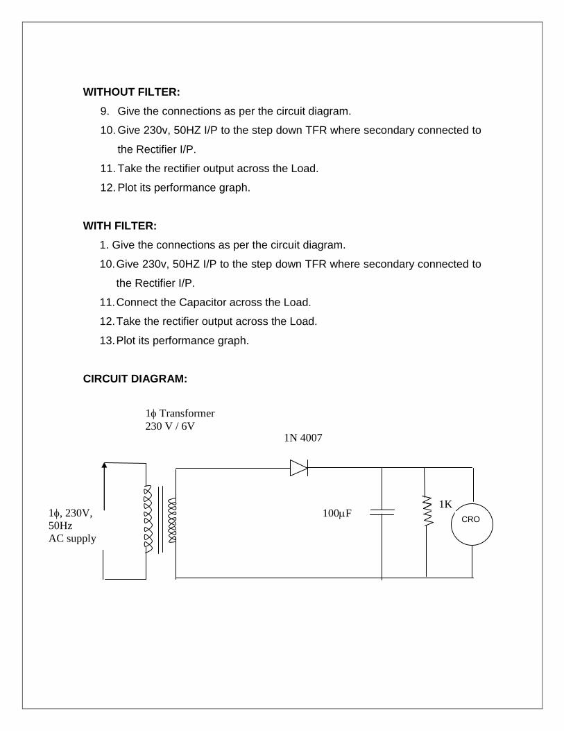
WITHOUT FILTER:
9. Give the connections as per the circuit diagram.
10. Give 230v, 50HZ I/P to the step down TFR where secondary connected to
the Rectifier I/P.
11. Take the rectifier output across the Load.
12. Plot its performance graph.
WITH FILTER:
1. Give the connections as per the circuit diagram.
10. Give 230v, 50HZ I/P to the step down TFR where secondary connected to
the Rectifier I/P.
11. Connect the Capacitor across the Load.
12. Take the rectifier output across the Load.
13. Plot its performance graph.
CIRCUIT DIAGRAM:
1 Transformer
230 V / 6V 1N 4007
1K 100F 1, 230V,
50Hz
AC supply
CRO

TABULAR COLUMN:
WITHOUT FILTER:
Vm Vrms Vdc Ripple factor Efficiency
WITH FILTER:
Vrms Vrpp Vdc Ripple factor Efficiency
MODEL GRAPH:
RESULT:
Thus the performance characteristics of 1 Half wave rectifier was obtained.
Ex.No.7b
Vin
(Volts)
t (ms)
Vo
(Volts)
t (ms)
t (ms)
Vo
(Volts)
Without Filter
With Filter

SINGLE PHASE FULL WAVE RECTIFIER
AIM:
To construct a Full wave rectifier using diode and to draw its performance
characteristics.
APPARATUS REQUIRED: COMPONENTS
REQUIRED:
S.
No. Name Range Type Qty
S.
No. Name Range Type Qty
1 Transformer 230/(6-0-6)V 1 1
Diode IN4001 2
2 R.P.S (0-30)V 2
3 Ammeter
(0–30)mA 1 2 Resistor 1K 1
(0–250)µA 1 3 Bread
Board
1
4 Voltmeter (0–30)V 1 4 Capacitor 100µf 1
(0–2)V 1 5 CRO 1
FORMULAE:
WITHOUT FILTER:
(i) Vrms = Vm / 2
(ii) Vdc = 2Vm /
(iii) Ripple Factor = (Vrms / Vdc)2 – 1
(iv) Efficiency = (Vdc / Vrms)2 x 100
WITH FILTER:
(i) Vrms = Vrpp /(2* 3)
(ii) Vdc = Vm – V rpp
(iv) Ripple Factor = Vrms’/ Vdc
PROCEDURE:
WITHOUT FILTER:
9. Give the connections as per the circuit diagram.

10. Give 230v, 50HZ I/P to the step down TFR where secondary connected
to the Rectifier I/P.
11. Take the rectifier output across the Load.
12. Plot its performance graph.
WITH FILTER:
1. Give the connections as per the circuit diagram.
10. Give 230v, 50HZ I/P to the step down TFR where secondary connected to
the Rectifier I/P.
11. Connect the Capacitor across the Load.
12. Take the rectifier output across the Load.
13. Plot its performance graph.
CIRCUIT DIAGRAM:
1N 4007
1K 100F
1, 230V,
50Hz
AC supply
CRO
1N 4007
1 Transformer
230 V / 6V

TABULAR COLUMN:
WITHOUT FILTER:
Vm Vrms Vdc Ripple factor Efficiency
WITH FILTER:
Vrms Vrpp Vdc Ripple factor Efficiency
MODEL GRAPH :
RESULT: Thus the performance characteristics of 1 Full wave rectifier were
obtained.
Ex.No.8
Vin
(Volts)
t (ms)
Vo
(Volts)
t (ms)
t (ms)
Vo
(Volts)
Without Filter
With Filter
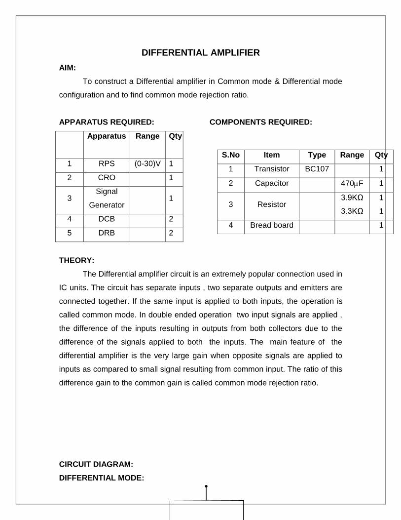
DIFFERENTIAL AMPLIFIER
AIM:
To construct a Differential amplifier in Common mode & Differential mode
configuration and to find common mode rejection ratio.
APPARATUS REQUIRED: COMPONENTS REQUIRED:
Apparatus Range Qty
1 RPS (0-30)V 1
2 CRO 1
3 Signal
Generator 1
4 DCB 2
5 DRB 2
THEORY:
The Differential amplifier circuit is an extremely popular connection used in
IC units. The circuit has separate inputs , two separate outputs and emitters are
connected together. If the same input is applied to both inputs, the operation is
called common mode. In double ended operation two input signals are applied ,
the difference of the inputs resulting in outputs from both collectors due to the
difference of the signals applied to both the inputs. The main feature of the
differential amplifier is the very large gain when opposite signals are applied to
inputs as compared to small signal resulting from common input. The ratio of this
difference gain to the common gain is called common mode rejection ratio.
CIRCUIT DIAGRAM:
DIFFERENTIAL MODE:
S.No Item Type Range Qty
1 Transistor BC107 1
2 Capacitor 470F 1
3 Resistor 3.9KΩ
3.3KΩ
1
1
4 Bread board 1

COMMON MODE:
9V
3.3 K
3.9K
Vo1 Vo2
V2
13V
3.9K
-9V

PROCEDURE:
DIFFERENTIAL MODE:
9. Connect the circuit as per the circuit diagram.
10. Set V1 = 50mv and V2 =55mv using the signal generator.
11. Find the corresponding output voltages across V01 & V02 using CRO
12. Calculate common mode rejection ratio using the given formula.
COMMON MODE:
9. Connect the circuit as per the circuit diagram.
10. Set V1 = 50mv using the signal generator.
11. Find the output voltage across Vo using multimeter.
12. Calculte common mode rejection ratio using the given formula.
CALCULATION:
Common mode rejection ratio(CMRR) = Ad / Ac
Ad = Differential mode gain
Ac = Common mode gain
Where Ad = Vo /Vd
Vo = Output voltage measured across CRO
Vd = V 1 – V2 , V 1 , V2 – input voltage applied.
Ac = Vo /Vc
Vc = (V 1 + V2 )/2
DIFFERENTIAL MODE:
V1 =
V2 =
Output voltage =
Vd= V1-V2 =
Ad=Vo/Vd =
RESULT: Thus the differential amplifier was constructed in common mode
and Differential mode configuration. Further common mode rejection ratio was
found
Exp. No: 12
COMMON MODE:
Input voltage =
Output voltage =
V1=V2 =
Vc=(V1+V2)/2 =

PASSIVE FILTERS
Aim:
To attenuate unwanted frequency components from input signal by using resistor
and capacitor.
Apparatus required:
S.No Name of the apparatus Range Type Quantity
1. Signal Generator 01
2. Resistor 01
3. Capacitor Ceramic 01
4. CRO 01
5. Breadboard 01
Theory:
A filter is an AC circuit that separates some frequencies from other in
within mixed – frequency signals. Audio equalizers and crossover networks are
two well-known applications of filter circuits. A Bode plot is a graph plotting
waveform amplitude or phase on one axis and frequency on the other.
A low-pass filter allows for easy passage of low-frequency signals from
source to load, and difficult passage of high-frequency signals. Capacitor low-pass
filters insert a resistor in series and a capacitor in parallel with the load as shown
in the circuit diagram. The former filter design tries to “block” the unwanted
frequency signal while the latter tries to short it out.
The cutoff frequency for a low-pass filter is that frequency at which the
output (load) voltage equals 70.7% of the input (Source) voltage. Above the cutoff
frequency, the output voltage is lower than 70.7% of the input, and vice-versa. See
the circuit diagram
1
Fcutoff = ----------

2RC
A high-pass filter allows for easy passage of high-frequency signals from source to
load, and difficult passage of low-frequency signals. Capacitor high-pass filters
insert a capacitor in series with the load as shown in the circuit diagram. The
former filter design tries to “brick” the unwanted frequency signal while the latter
tries to short it out.
The cutoff frequency for a high-pass filter is that frequency at which the
output (load) voltage equals 70.7% of the input (source) voltage. Above the cutoff
frequency, the output voltage is greater than 70.7% of the input, and vice-versa.
1
Fcutoff = ----------
2RC
A band – pass filter works to screen out frequencies that are too low or too
high, giving easy passage only to frequencies within a certain range. Stacking a
low-pass filter on the end of a high-pass filter, or vice-versa can make band-pass
filters. Refer the circuit diagrams
Fig. 7.6
“Attenuate” means to reduce or diminish in amplitude. When you
turn down the volume control on your stereo, you are “attenuating” the signal
being sent to the speakers.
A band-stop filter works to screen out frequencies that are within a certain
range, giving easy passage only to frequencies outside of that range. Also known
as band-elimination, band-reject, or notch filters.
Placing a low-pass filter in parallel with a high-pass filter can make band-
stop filters. Commonly, both the low-pass and high-pass filter sections are of the
Signal
input
Low-pass filter High-pass filter Signal
output Blocks frequencies
that are too high
Blocks frequencies
that are too low

Signal
Input
Low-pass filter
High-pass filter
Signal
Output
“T” configuration giving the name “Twin-T” to the band-stop combination. Refer
the fig.7.7, 7.8a and 7.8b.
Passes low frequencies
Passes high frequencies
Fig. 7.8a
The frequency of maximum attenuation is called the notch
frequency.
Procedure:
13. Give the connections as per circuit diagrams.
14. Switch on the main.
15. Change the frequency from minimum and find the output
voltage by using CRO.
16. Draw the graph.
17. Verify the cut off frequency.
18. Switch off the main.
Result:
Thus we analyze passive filter and various waveforms are noted
Exp. No : 10
STUDY OF CRO AND
POWER FACTOR MEASUREMENT USING CRO
Aim:
To study cathode Ray Oscilloscope (CRO) and measurement of power factor using
CRO.

Apparatus required:
S.No Name of the apparatus Range Type Quantity
1. Resistance Box 1
2. Capacitance Box 1
3. Inductance Box 1
4. Function Generator 1
5. Bread board 1
Theory:
The cathode ray oscilloscope is the most versatile measuring instrument
available. We can measure following parameters using the CRO:
9. AC or DC voltage.
10. Time (t=1/f).
11. Phase relationship
12. Waveform calculation: Rise time; fall time; on time; off-time
Distortion, etc.
We can also measure non-electrical physical quantities like pressure, strain,
temperature, acceleration, etc., by converting into electrical quantities using
a transducer.
Major blocks:
13. Cathode ray tube (CRT)
14. Vertical amplifier
15. Horizontal amplifier
16. Sweep generator
17. Trigger circuit
18. Associated power supply.
11. The cathode ray tube is the heart of CRO. The CRT is enclosed in an
evacuated glass envelope to permit the electron beam to traverse in the
tube easily. The main functional units of CRO are as follows.
Electron gun assembly
Deflection plate unit
Screen.
12. Vertical Amplifier is the main factor in determining the bandwidth and
sensitivity of an oscilloscope. Vertical sensitivity is a measure of how
much the electron beam will be deflected for a specified input signal.
On the front panel of the oscilloscope, one can see a knob attached to a
rotary switch labeled volts/division. The rotary switch is electrically
connected to the input attenuation network. The setting of the rotary
switch indicates what amplitude signal is required to deflect the beam
vertically by one division.
13. Horizontal amplifier Under normal mode of operation, the horizontal
amplifier will amplify the sweep generator input. When the CRO is
being used in the X-Y mode, the horizontal amplifier will amplify the
signal applied to the horizontal input terminal. Although the vertical
amplifier mush be able to faithfully reproduce low-amplitude and high
frequency signal with fast rise-time, the horizontal amplifier is only
required to provide a faithful reproduction of the sweep signal which
has a relatively high amplitude and slow rise time.
14. Sweep generator and Trigger circuit These two units form the Signal
Synchronization unit of the CRO.
15. Associated Power Supply: The input signal may come from an
external source when the trigger selector switch is set to EXT or from
low amplitude AC voltage at line frequency when the switch is set to
LINE or from the vertical amplifier when the switch is set to INT. When
set for INT (internal triggering), the trigger circuit receives its inputs
from the vertical amplifier.

Major Blocks in a Practical CRO
A CRO consists of a cathode ray tube (CRT) and additional control knobs.
The main parts of a CRT are:
7. Electron gun assembly.
8. Deflection plate assembly.
9. Fluorescent screen.
Electron Gun Assembly: The electron gun assembly produces a sharp beam of
electrons, which are accelerated to high velocity. This focused beam of electrons
strike the fluorescent screen with sufficient energy to cause a luminous spot on the
screen.
Deflection plate assembly: This part consists of two plates in which one pair of
plates is placed horizontally and other of plates is placed vertically. The signal
under test is applied to vertical deflecting plates. The horizontal deflection plates
are connected to a built-in ramp generator, which moves the luminous spot
periodically in a horizontal direction from left to right over the screen. These two
deflection plates give stationary appearance to the waveform on the screen. CRO
operates on voltage. Since the deflection of the electron beam is directly
proportional to the deflecting voltage, the CRT may be used as a linear measuring
device. The voltage being measured is applied to the vertical plates through an
iterative network, whose propagation time corresponds to the velocity of electrons,
thereby synchronizing the voltage applied to the vertical plate with the velocity of
the beam.
Synchronization of input signal: The sweep generator produces a saw tooth
waveform, which is used to synchronize the applied voltage to obtain a stationary-
applied signal. This requires that the time base be operated at a submultiples
frequency of the signal under measurement. If synchronization is not done, the
pattern is not stationary, but appears to drift across the screen in a random fashion.
Internal synchronization This trigger is obtained from the time base generator to
synchronize the signal.
External synchronization An external trigger source can also be used to
synchronize the signal being measured.
Auto Triggering Mode The time base used in this case in a self-oscillating
condition, i.e., it gives an output even in the absence of any Y-input. The
advantage of this mode is that the beam is visible on the screen under all
conditions, including the zero input. When the input exceeds a certain magnitude
then the internal free running oscillator locks on to the frequency.
Precautions:
5. The ammeter is connected using thick wires.
6. While reversing ammeter polarity, see to it that the capacitor is not
discharged.
Observation:
Sl.No Time Voltage Current
Unit (Sec) (Volts) (Amps)
Result: Thus we study about CRO & to measure p.f
CLASS : II YEAR/ III SEMSESTER
SUBJECT CODE : 131351
SUBJECT : ELECTRON DEVICES AND CIRCUITS LAB
BATCH : B2
STAFF IN-CHARGE: Mrs. A. SANGARI
DESIGNATION : SENIOR LECTURER
STAFF CODE : EE52

LIST OF EXPERIMENTS
131351 ELECTRON DEVICES AND CIRCUITS LABORATORY L T P C (B.E. (EEE), B.E. (E&I) and B.E. (I & C) 0 0 3 2 (Revised)
37. Characteristics of semiconductor diode and zener diode .
38. Characteristics of transistor under CE, CB and CC .
39. Characteristics of FET .
40. Characteristics of UJT .
41. Characteristics of SCR, DIAC and TRIAC.
42. Photodiode, Phototransistor characteristics and study of light
activated relay circuit.
43. Static characteristics of Thermistors.
44. Single phase half wave and full wave rectifiers with inductive and
capacitive filters.
45. Differential amplifiers using FET.
46. Study of CRO.
47. Series and parallel resonance circuits.
48. Realization of passive filters.
Ex.No.1a
CHARACTERISTICS OF PN JUNCTION DIODE
AIM:
To study the PN junction diode characteristics under Forward & Reverse
bias conditions.
APPARATUS REQUIRED: COMPONENTS REQUIRED:
S.No. Name Range Type Qty
S.No. Name Range Type Qty
1 R.P.S 1 Diode
2 Ammeter
2 Resistor
3 Bread
Board
3 Voltmeter 4 Wires
THEORY:
A PN junction diode is a two terminal junction device. It conducts only in
one direction (only on forward biasing).
FORWARD BIAS:
On forward biasing, initially no current flows due to barrier potential. As the
applied potential exceeds the barrier potential the charge carriers gain sufficient
energy to cross the potential barrier and hence enter the other region. The holes,
which are majority carriers in the P-region, become minority carriers on entering
the N-regions, and electrons, which are the majority carriers in the N-region,
become minority carriers on entering the P-region. This injection of Minority
carriers results in the current flow, opposite to the direction of electron
movement.
REVERSE BIAS:
On reverse biasing, the majority charge carriers are attracted towards the
terminals due to the applied potential resulting in the widening of the depletion
region. Since the charge carriers are pushed towards the terminals no current
flows in the device due to majority charge carriers. There will be some current in
the device due to the thermally generated minority carriers. The generation of
such carriers is independent of the applied potential and hence the current is
constant for all increasing reverse potential. This current is referred to as
Reverse Saturation Current (IO) and it increases with temperature. When the
applied reverse voltage is increased beyond the certain limit, it results in
breakdown. During breakdown, the diode current increases tremendously.
PROCEDURE:
FORWARD BIAS:
13. Connect the circuit as per the diagram.
14. Vary the applied voltage V in steps of 0.1V.
15. Note down the corresponding Ammeter readings I.
16. Plot a graph between V & I
OBSERVATIONS
10. Find the d.c (static) resistance = V/I.
11. Find the a.c (dynamic) resistance r = V / I (r = V/I) = 12
12
II
VV
.
12. Find the forward voltage drop = [Hint: it is equal to 0.7 for Si and 0.3 for
Ge]
REVERSE BIAS:
16. Connect the circuit as per the diagram.
17. Vary the applied voltage V in steps of 1.0V.
18. Note down the corresponding Ammeter readings I.
19. Plot a graph between V & I
20. Find the dynamic resistance r = V / I.

(0-100)mA, MC
+ -
+
+
-
+
(0-15)V, MC +
-
+
(0-10)V
RPS
(0-500)µA,MC
+ -
+
+
-
+
(0-30)V, MC +
-
+
(0-30)V
RPS
FORMULA FOR REVERSE SATURATION CURRENT (IO):
Io = I/[exp(V/VT)]-1
Where VT is the voltage equivalent of Temperature = kT/q
-k is Boltzmann’s constant, q is the charge of the electron and T is the
temperature in degrees Kelvin.
=1 for Silicon and 2 for Germanium
CIRCUIT DIAGRAM:
FORWARD BIAS:
REVERSE BIAS:
Specification for 1N4001: Silicon Diode
Peak Inverse Voltage: 50V
470 a
a
a
a
a
A
A
A
470 a
a
a
a
a
A
A
A

Idc = 1A.
Maximum forward voltage drop at 1 Amp is 1.1 volts
Maximum reverse current @50 volts is 5A
TABULAR COLUMN:
FORWARD BIAS: REVERSE BIAS:
MODEL GRAPH
If (mA)
I2
Vb I1
( Volts) V1 V2 Vf
(Volts)
Ir (A)
RESULT:
Forward and Reverse bias characteristics of the PN junction diode and the
dynamic resistance under
S.No. VOLTAGE
(In Volts)
CURRENT
(In mA)
S..No. VOLTAGE
(In Volts)
CURRENT
(In A)

i) Forward bias = ---------------------
ii) Reverse bias = ----------------------.
iii) Reverse Saturation Current = ----------------.

Ex.No.1b
CHARACTERISTICS OF ZENER DIODE
AIM:
To determine the breakdown voltage of a given zener diode.
APPARATUS REQUIRED: COMPONENTS REQUIRED:
S.No. Name Range Type Qty
S.No. Name Range Type Qty
1 R.P.S 1 zener
diode
2 Ammeter
2 Resistor
3 Bread
Board
3 Voltmeter 4 Wires
THEORY:
A properly doped crystal diode, which has a sharp breakdown voltage, is known
as zener diode.
FORWARD BIAS:
On forward biasing, initially no current flows due to barrier potential. As the
applied potential increases, it exceeds the barrier potential at one value and the
charge carriers gain sufficient energy to cross the potential barrier and enter the
other region. the holes ,which are majority carriers in p-region, become minority
carriers on entering the N-regions and electrons, which are the majority carriers
in the N-regions become minority carriers on entering the P-region. This injection
of minority carriers results current, opposite to the direction of electron
movement.
REVERSE BIAS:
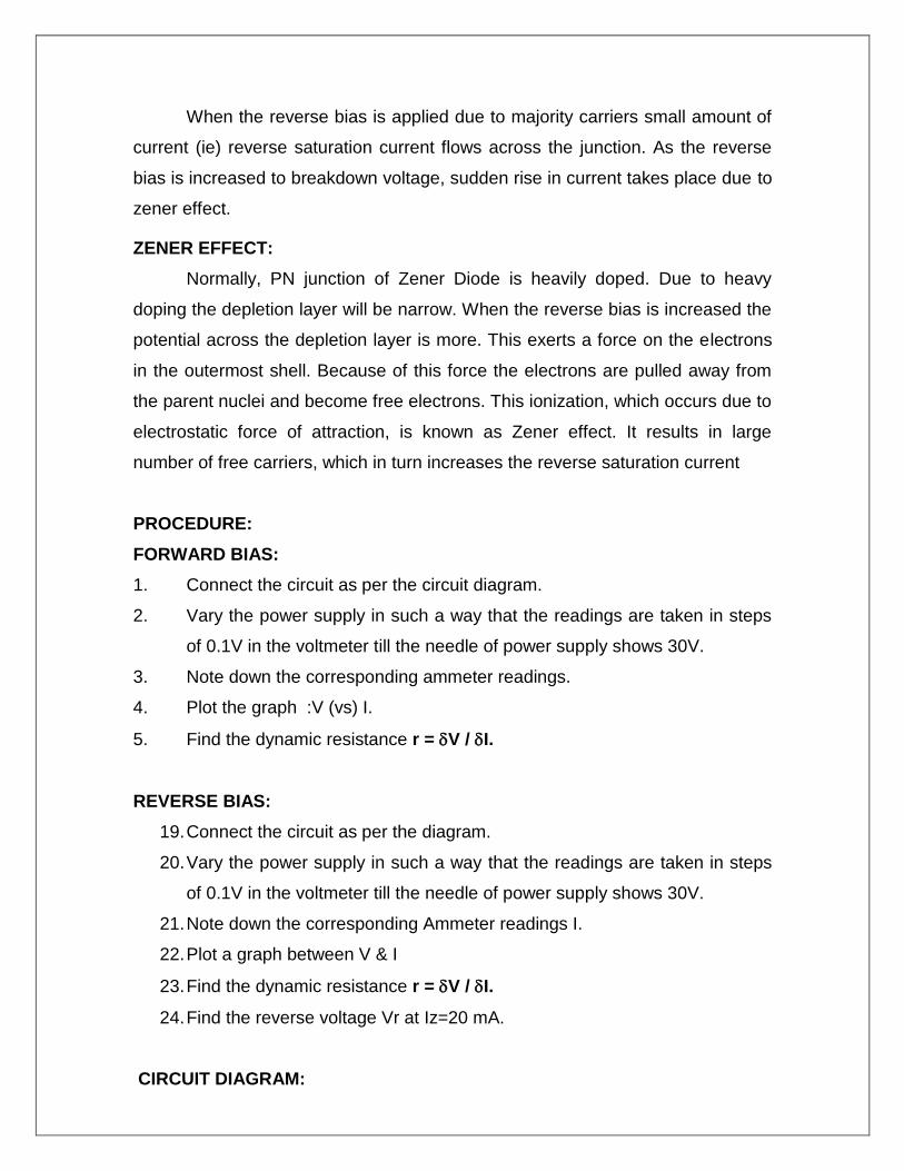
When the reverse bias is applied due to majority carriers small amount of
current (ie) reverse saturation current flows across the junction. As the reverse
bias is increased to breakdown voltage, sudden rise in current takes place due to
zener effect.
ZENER EFFECT:
Normally, PN junction of Zener Diode is heavily doped. Due to heavy
doping the depletion layer will be narrow. When the reverse bias is increased the
potential across the depletion layer is more. This exerts a force on the electrons
in the outermost shell. Because of this force the electrons are pulled away from
the parent nuclei and become free electrons. This ionization, which occurs due to
electrostatic force of attraction, is known as Zener effect. It results in large
number of free carriers, which in turn increases the reverse saturation current
PROCEDURE:
FORWARD BIAS:
1. Connect the circuit as per the circuit diagram.
2. Vary the power supply in such a way that the readings are taken in steps
of 0.1V in the voltmeter till the needle of power supply shows 30V.
3. Note down the corresponding ammeter readings.
4. Plot the graph :V (vs) I.
5. Find the dynamic resistance r = V / I.
REVERSE BIAS:
19. Connect the circuit as per the diagram.
20. Vary the power supply in such a way that the readings are taken in steps
of 0.1V in the voltmeter till the needle of power supply shows 30V.
21. Note down the corresponding Ammeter readings I.
22. Plot a graph between V & I
23. Find the dynamic resistance r = V / I.
24. Find the reverse voltage Vr at Iz=20 mA.
CIRCUIT DIAGRAM:
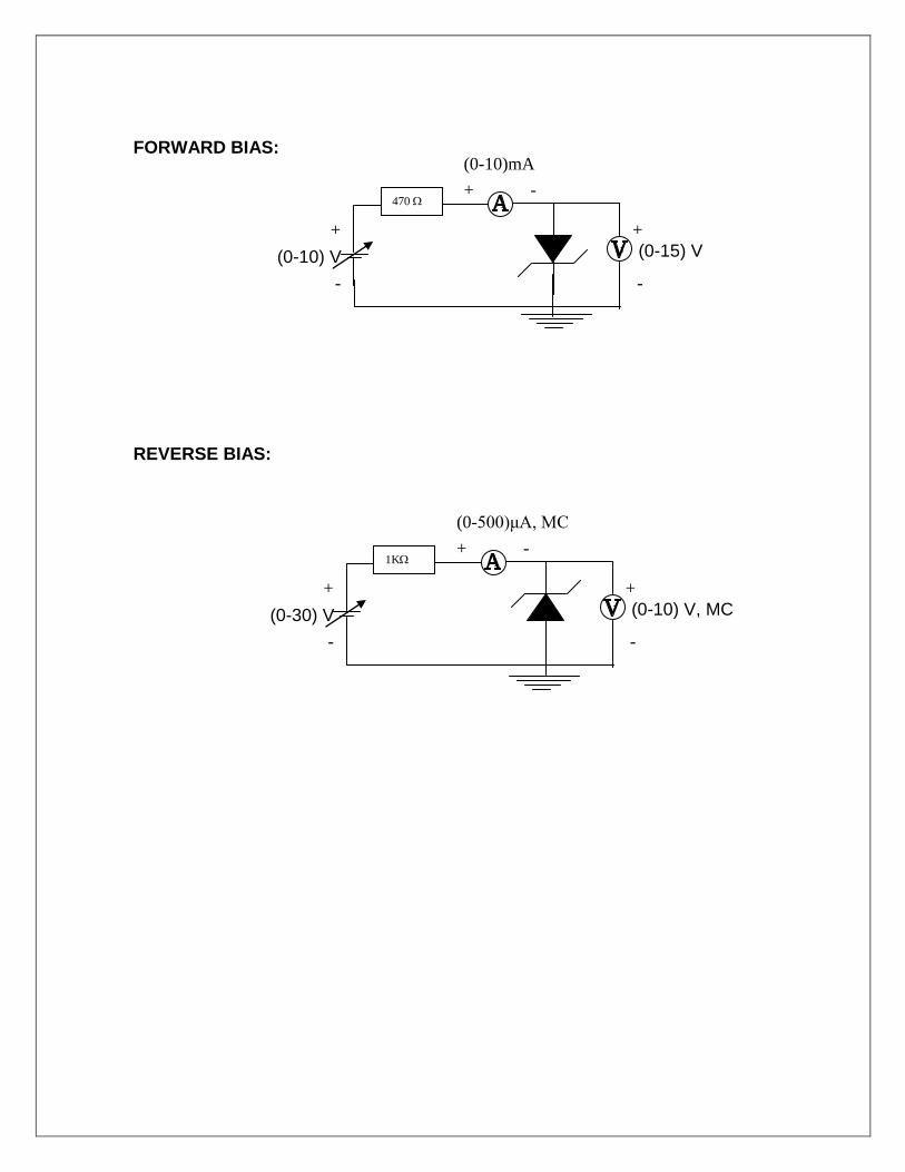
(0-15) V
+ -
+
-
+
-
(0-10) V
(0-10) V, MC
+ -
+
-
+
-
(0-30) V
FORWARD BIAS:
REVERSE BIAS:
1K
a
a
a
a
a
A
A
A
a
a
a
a
a
A
A
A
470
aaaa
aAA
A
aaaa
aAA
A
a
a
a
a
a
A
A
A
(0-10)mA
1
K
a
a
a
a
a
A
A
A
a
a
a
a
a
A
A
A
1K
aaaa
aAA
A
aaaa
aAA
A
a
a
a
a
a
A
A
A
(0-500)μA, MC
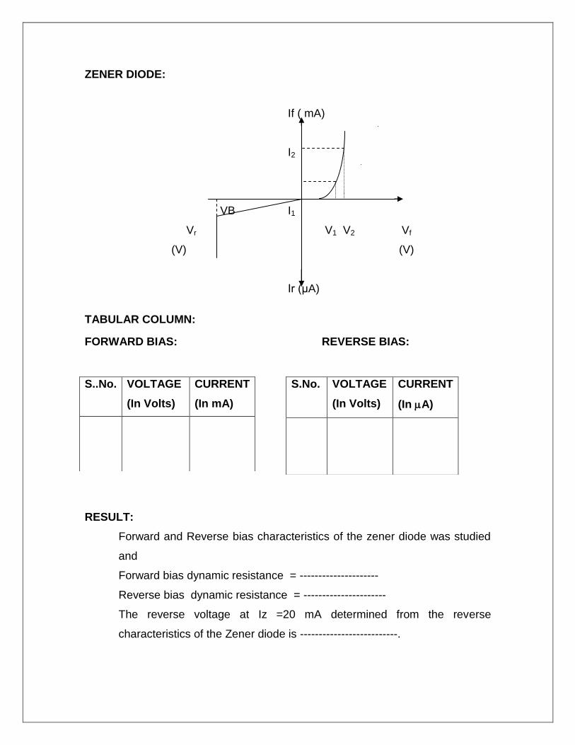
ZENER DIODE:
If ( mA)
I2
VB I1
Vr V1 V2 Vf
(V) (V)
Ir (μA)
TABULAR COLUMN:
FORWARD BIAS: REVERSE BIAS:
RESULT:
Forward and Reverse bias characteristics of the zener diode was studied
and
Forward bias dynamic resistance = ---------------------
Reverse bias dynamic resistance = ----------------------
The reverse voltage at Iz =20 mA determined from the reverse
characteristics of the Zener diode is --------------------------.
S..No. VOLTAGE
(In Volts)
CURRENT
(In mA)
S.No. VOLTAGE
(In Volts)
CURRENT
(In A)

Ex. No. 2a
CHARACTERISTICS OF CE CONFIGURATION USING BJT
AIM:
To plot the transistor characteristics of CE configuration.
APPARATUS REQUIRED: COMPONENTS REQUIRED:
S.No. Name Range Type Qty
S.No. Name Range Type Qty
1 R.P.S 1 Transistor
2 Ammeter
2 Resistor
3 Bread
Board
3 Voltmeter 4 Wires
THEORY:
A BJT is a three terminal two – junction semiconductor device in which the
conduction is due to both the charge carrier. Hence it is a bipolar device and it
amplifier the sine waveform as they are transferred from input to output. BJT is
classified into two types – NPN or PNP. A NPN transistor consists of two N
types in between which a layer of P is sandwiched. The transistor consists of
three terminal emitter, collector and base. The emitter layer is the source of the
charge carriers and it is heartily doped with a moderate cross sectional area.
The collector collects the charge carries and hence moderate doping and large
cross sectional area. The base region acts a path for the movement of the
charge carriers. In order to reduce the recombination of holes and electrons the
base region is lightly doped and is of hollow cross sectional area. Normally the
transistor operates with the EB junction forward biased.

Bottom View BC107 Specification: BC107/50V/0.1A,0.3W,300MHz
(0 – 30)mA 1 K
In transistor, the current is same in both junctions, which indicates that
there is a transfer of resistance between the two junctions. One to this fact the
transistor is known as transfer resistance of transistor.
PROCEDURE:
INPUT CHARACTERISTICS:
10. Connect the circuit as per the circuit diagram.
11. Set VCE, vary VBE in regular interval of steps and note down the
corresponding IB reading. Repeat the above procedure for different values of
VCE.
12. Plot the graph: VBE Vs IB for a constant VCE.
OUTPUT CHARACTERISTICS:
10. Connect the circuit as per the circuit diagram.
11. Set IB, Vary VCE in regular interval of steps and note down the
corresponding IC reading. Repeat the above procedure for different
values of IB.
12. Plot the graph: VCE Vs IC for a constant IB.
PIN DIAGRAM:
B
E C
CIRCUIT DIAGRAM:

(0 – 250) A
10 K
- +
BC107
10 KΩ
+
-
+
+
-
+
(0-30)V
+
-
+
+
-
+
+ -
+
(0-30)V
(0-30)V
(0-1)V
MODEL GRAPH:
INPUT CHARACTERISTICS: OUTPUT CHARACTERISTICS:
TABULAR COLUMN:
INPUT CHARACTERISTICS:
A
A
V
V
C
E
C
B
C
VCE = 0V
VCE = 5V
IB
µA mA
VBE(V) VCE(V)
0 0
IB=60A
IB=40A
IB=20A
IC

VCE=1V VCE=2V
VBE(V) IB(μA) VBE(V) IB(μA)
OUTPUT CHARACTERISTICS:
IB=20A IB=40A
VCE(V) IC(mA) VCE(V) IC(mA)
RESULT:
The transistor characteristics of a Common Emitter (CE)
configuration were plotted
Ex.No.2b
CHARACTERISTICS OF CB CONFIGURATION USING BJT
AIM:
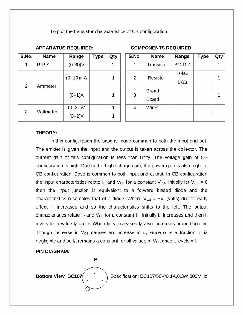
To plot the transistor characteristics of CB configuration.
APPARATUS REQUIRED: COMPONENTS REQUIRED:
S.No. Name Range Type Qty
S.No. Name Range Type Qty
1 R.P.S (0-30)V 2 1 Transistor BC 107 1
2 Ammeter
(0–10)mA 1 2 Resistor 10k
1K
1
(0–1)A 1 3 Bread
Board
1
3 Voltmeter (0–30)V 1 4 Wires
(0–2)V 1
THEORY:
In this configuration the base is made common to both the input and out.
The emitter is given the input and the output is taken across the collector. The
current gain of this configuration is less than unity. The voltage gain of CB
configuration is high. Due to the high voltage gain, the power gain is also high. In
CB configuration, Base is common to both input and output. In CB configuration
the input characteristics relate IE and VEB for a constant VCB. Initially let VCB = 0
then the input junction is equivalent to a forward biased diode and the
characteristics resembles that of a diode. Where VCB = +VI (volts) due to early
effect IE increases and so the characteristics shifts to the left. The output
characteristics relate IC and VCB for a constant IE. Initially IC increases and then it
levels for a value IC = IE. When IE is increased IC also increases proportionality.
Though increase in VCB causes an increase in , since is a fraction, it is
negligible and so IC remains a constant for all values of VCB once it levels off.
PIN DIAGRAM:
B
Bottom View BC107 Specification: BC107/50V/0.1A,0.3W,300MHz
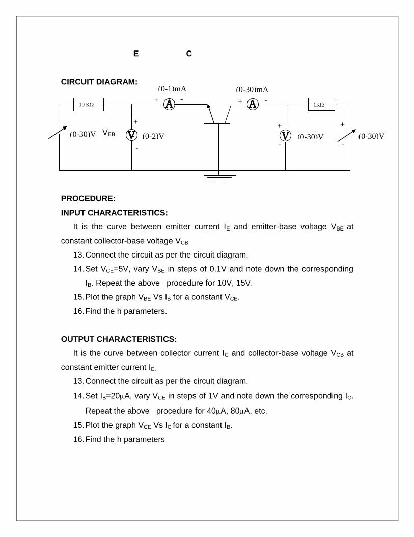
(0-30)V
(0-1)mA
+ -
+
(0-30)mA
+ -
+
+
-
+
+
-
+
+
-
+
(0-2)V (0-30)V (0-30)V
E C
CIRCUIT DIAGRAM:
-
PROCEDURE:
INPUT CHARACTERISTICS:
It is the curve between emitter current IE and emitter-base voltage VBE at
constant collector-base voltage VCB.
13. Connect the circuit as per the circuit diagram.
14. Set VCE=5V, vary VBE in steps of 0.1V and note down the corresponding
IB. Repeat the above procedure for 10V, 15V.
15. Plot the graph VBE Vs IB for a constant VCE.
16. Find the h parameters.
OUTPUT CHARACTERISTICS:
It is the curve between collector current IC and collector-base voltage VCB at
constant emitter current IE.
13. Connect the circuit as per the circuit diagram.
14. Set IB=20A, vary VCE in steps of 1V and note down the corresponding IC.
Repeat the above procedure for 40A, 80A, etc.
15. Plot the graph VCE Vs IC for a constant IB.
16. Find the h parameters
a
a
a
a
a
A
A
A
10 K
a
a
a
a
a
A
A
A
a
a
a
a
a
A
A
A
a
a
a
a
a
A
A
A
a
a
a
a
a
A
A
A
a
a
a
a
a
A
A
A
1K
VEB

TABULAR COLUMN:
INPUT CHARACTERISTICS:
S.No. VCB = V VCB = V VCB = V
VEB
(V)
IE
(A)
VEB
(V)
IE
(A)
VEB
(V)
IE
(A)
OUTPUT CHARACTERISTICS:
S.No. IE= mA IE= mA IE= mA
VCB
(V)
Ic
(mA)
VCB
(V)
Ic
(mA)
VCB
(V)
Ic
(mA)
MODEL GRAPH:
INPUT CHARACTERISTICS:

IC
(mA)
VCB1
IE2
VCB2
IE1 VEB1 VEB2 VEB (V)
OUTPUT CHARACTERISTICS:
IC
(mA) IE3
IC2 IE2
IC1
IE1
VCB1 VCB2 VCB (V)
RESULT:
The transistor characteristics of a Common Base (CB) configuration were
plotted and uses studied.
Ex.No.2c
CHARACTERISTICS OF CC CONFIGURATION USING BJT
AIM:
To plot the transistor characteristics of CE configuration.
APPARATUS REQUIRED: COMPONENTS REQUIRED:
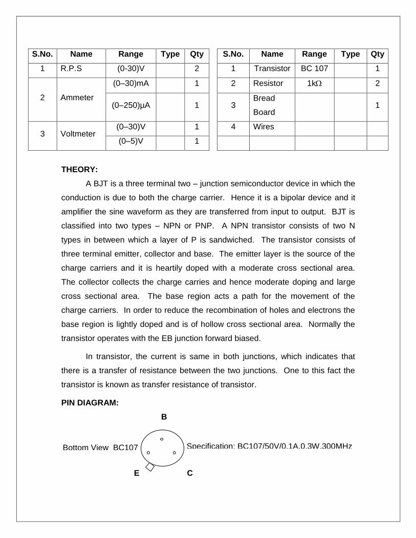
Bottom View BC107 Specification: BC107/50V/0.1A,0.3W,300MHz
S.No. Name Range Type Qty
S.No. Name Range Type Qty
1 R.P.S (0-30)V 2 1 Transistor BC 107 1
2 Ammeter
(0–30)mA 1 2 Resistor 1k 2
(0–250)µA 1 3 Bread
Board
1
3 Voltmeter (0–30)V 1 4 Wires
(0–5)V 1
THEORY:
A BJT is a three terminal two – junction semiconductor device in which the
conduction is due to both the charge carrier. Hence it is a bipolar device and it
amplifier the sine waveform as they are transferred from input to output. BJT is
classified into two types – NPN or PNP. A NPN transistor consists of two N
types in between which a layer of P is sandwiched. The transistor consists of
three terminal emitter, collector and base. The emitter layer is the source of the
charge carriers and it is heartily doped with a moderate cross sectional area.
The collector collects the charge carries and hence moderate doping and large
cross sectional area. The base region acts a path for the movement of the
charge carriers. In order to reduce the recombination of holes and electrons the
base region is lightly doped and is of hollow cross sectional area. Normally the
transistor operates with the EB junction forward biased.
In transistor, the current is same in both junctions, which indicates that
there is a transfer of resistance between the two junctions. One to this fact the
transistor is known as transfer resistance of transistor.
PIN DIAGRAM:
B
E C

+
-
+
-
+
+ -
+
+ +
-
+
+
+ -
+
(0-30)mA
(0-250)µA
CIRCUIT DIAGRAM:
PROCEDURE:
INPUT CHARECTERISTICS:
10. Connect the circuit as per the circuit diagram.
11. Set VCE, vary VBE in regular interval of steps and note down the
corresponding IB reading. Repeat the above procedure for different values
of VCE.
12. Plot the graph: VBC Vs IB for a constant VCE.
OUTPUT CHARECTERISTICS:
10. Connect the circuit as per the circuit diagram.
11. Set IB, Vary VCE in regular interval of steps and note down the
corresponding IC reading. Repeat the above procedure for different
values of IB.
12. Plot the graph: VCE Vs IC for a constant IB.
MODEL GRAPH:
INPUT CHARACTERISTICS: OUTPUT CHARACTERISTICS:
A
A V
V
1 K
+
-
+
(0-30)V (0-30)V
(0-30)V (0-30)V
1 K

(A) (mA)
IB Ie
VCE=0 VCE=5V IB=60A
IB=40A
IB=20A
0 VBC(V) 0 VCE(V)
TABULAR COLUMN:
INPUT CHARACTERISTICS:
VCE=1V VCE=2V
VBC(V) IB(μA) VBC(V) IB(μA)
OUTPUT CHARACTERISTICS:
IB=20A IB=40A
VCE(V) IE(mA) VCE(V) IE(mA)
RESULT:

The transistor characteristics of a Common Emitter (CC) configuration
were plotted.

Ex.No.3
CHARACTERISTICS OF JUNCTION FIELD EFFECT TRANSISTOR
AIM:
To Plot the characteristics of given FET & determine rd, gm, , IDSS,VP.
APPARATUS REQUIRED: COMPONENTS REQUIRED:
S.No. Name Range Type Qty
S.No. Name Range Type Qty
1 R.P.S (0-30)V 2 1 FET BFW10 1
2 Ammeter (0–30)mA 1 2 Resistor 1k
68K
1
1
3 Voltmeter (0–30)V 1 3
Bread
Board
1
(0-10)V 1 4 Wires
THEORY:
FET is a voltage operated device. It has got 3 terminals. They are Source,
Drain & Gate. When the gate is biased negative with respect to the source, the
pn junctions are reverse biased & depletion regions are formed. The channel is
more lightly doped than the p type gate, so the depletion regions penetrate
deeply in to the channel. The result is that the channel is narrowed, its resistance
is increased, & ID is reduced. When the negative bias voltage is further
increased, the depletion regions meet at the center & ID is cutoff completely.
PROCEDURE:
DRAIN CHARACTERISTICS:
16. Connect the circuit as per the circuit diagram.
17. Set the gate voltage VGS = 0V.
18. Vary VDS in steps of 1 V & note down the corresponding ID.
19. Repeat the same procedure for VGS = -1V.

+ (0-30)V
68K
V
+
(0-30)V
(0-30)V
1k (0-30mA)
D G
S
BFW10
-
+ (0-10)V V
A
V
-
20. Plot the graph VDS Vs ID for constant VGS.
OBSERVATIONS
10. d.c (static) drain resistance, rD = VDS/ID.
11. a.c (dynamic) drain resistance, rd = VDS/ID.
12. Open source impedance, YOS = 1/ rd.
TRANSFER CHARACTERISTICS:
16. Connect the circuit as per the circuit diagram.
17. Set the drain voltage VDS = 5 V.
18. Vary the gate voltage VGS in steps of 1V & note down the corresponding ID.
19. Repeat the same procedure for VDS = 10V.
20. Plot the graph VGS Vs ID for constant VDS.
FET PARAMETER CALCULATION:
Drain Resistancd rd = GS
D
DS VI
V
Transconductance gm = DS
GS
D VV
I
Amplification factor μ=rd . gm
CIRCUIT DIAGRAM:

I D (
mA
)
PIN DIAGRAM:
BOTTOM VIEW OF BFW10:
SPECIFICATION:
Voltage : 30V, IDSS > 8mA.
MODEL GRAPH:
DRAIN CHARACTERISTICS:
TRANSFER CHARACTERISTICS:
ID(mA)
VDS =Const
VGS (V)
TABULAR COLUMN:
0
VGS = 0V
VGS = -1V
VGS = -2V
VGS = -3V
VDS (volts)
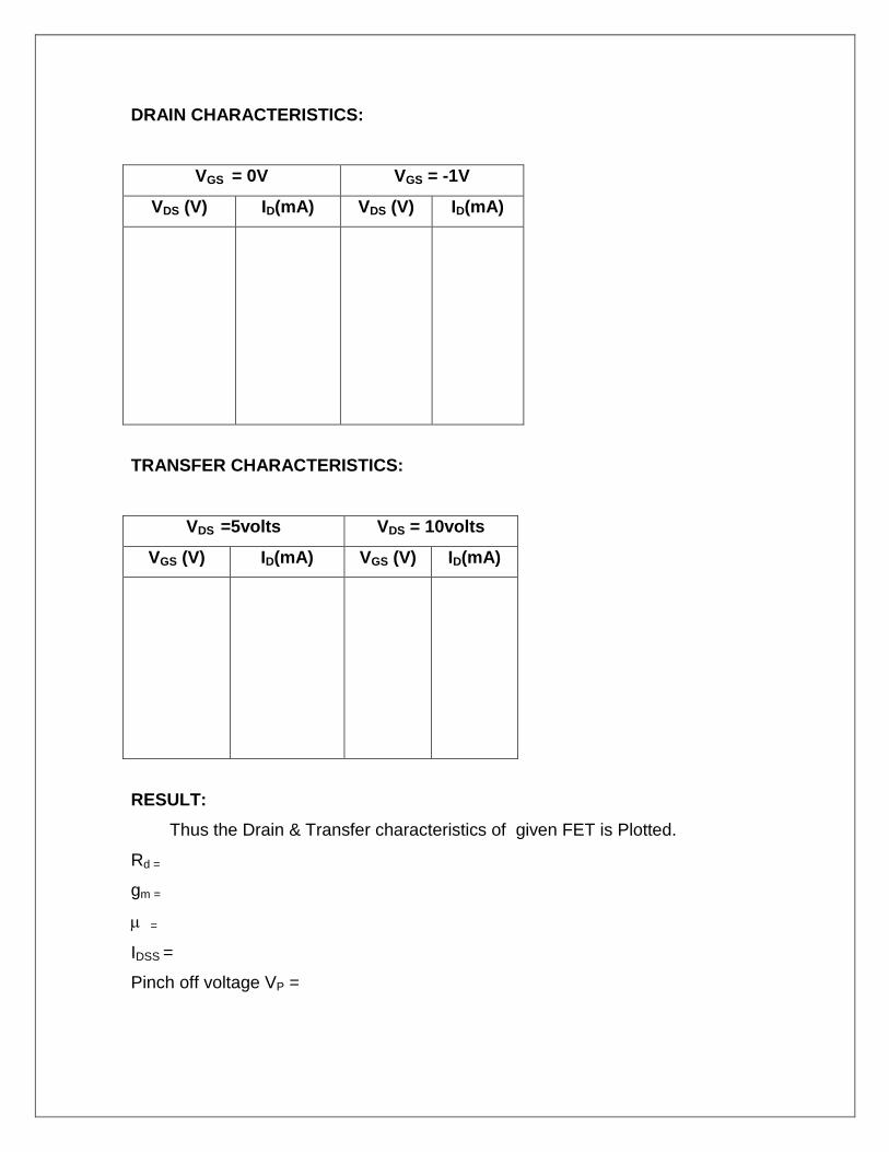
DRAIN CHARACTERISTICS:
VGS = 0V VGS = -1V
VDS (V) ID(mA) VDS (V) ID(mA)
TRANSFER CHARACTERISTICS:
RESULT:
Thus the Drain & Transfer characteristics of given FET is Plotted.
Rd =
gm =
=
IDSS =
Pinch off voltage VP =
VDS =5volts VDS = 10volts
VGS (V) ID(mA) VGS (V) ID(mA)
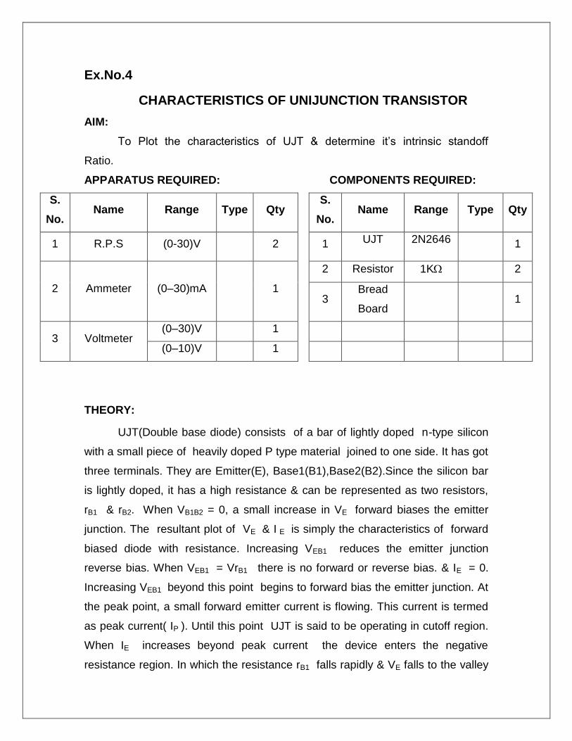
Ex.No.4
CHARACTERISTICS OF UNIJUNCTION TRANSISTOR
AIM:
To Plot the characteristics of UJT & determine it’s intrinsic standoff
Ratio.
APPARATUS REQUIRED: COMPONENTS REQUIRED:
S.
No. Name Range Type Qty
S.
No. Name Range Type Qty
1 R.P.S (0-30)V 2 1 UJT 2N2646 1
2 Ammeter (0–30)mA 1
2 Resistor 1K 2
3 Bread
Board
1
3 Voltmeter (0–30)V 1
(0–10)V 1
THEORY:
UJT(Double base diode) consists of a bar of lightly doped n-type silicon
with a small piece of heavily doped P type material joined to one side. It has got
three terminals. They are Emitter(E), Base1(B1),Base2(B2).Since the silicon bar
is lightly doped, it has a high resistance & can be represented as two resistors,
rB1 & rB2. When VB1B2 = 0, a small increase in VE forward biases the emitter
junction. The resultant plot of VE & I E is simply the characteristics of forward
biased diode with resistance. Increasing VEB1 reduces the emitter junction
reverse bias. When VEB1 = VrB1 there is no forward or reverse bias. & IE = 0.
Increasing VEB1 beyond this point begins to forward bias the emitter junction. At
the peak point, a small forward emitter current is flowing. This current is termed
as peak current( IP ). Until this point UJT is said to be operating in cutoff region.
When IE increases beyond peak current the device enters the negative
resistance region. In which the resistance rB1 falls rapidly & VE falls to the valley

B2
E
voltage.Vv. At this point IE = Iv. A further increase of IE causes the device to
enter the saturation region.
PROCEDURE:
16. Connect the circuit as per the circuit diagram.
17. Set VB1B2 = 0V, vary VEB1 , & note down the readings of IE & VEB1
18. Set VB1B2 = 10V , vary VEB1 , & note down the readings of IE & VEB1
19. Plot the graph : IE Versus VEB1 for constant VB1B2.
20. Find the intrinsic standoff ratio.
CIRCUIT DIAGRAM:
PIN DIAGRAM:
BOTTOM VIEW OF 2N2646:
SPECIFICATION FOR 2N2646:
* Inter base resistance RBB = 4.7 to 9.1 K
* Minimum Valley current = 4 mA
B2
(0-30)V (0-30)V
(0-30)V
1KΩ 1KΩ
(0-30)V
(0-30)mA
V V
A
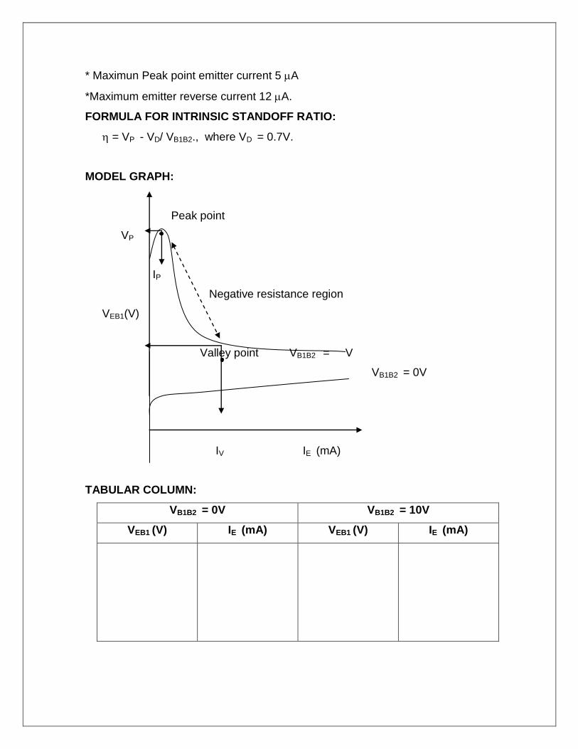
* Maximun Peak point emitter current 5 A
*Maximum emitter reverse current 12 A.
FORMULA FOR INTRINSIC STANDOFF RATIO:
= VP - VD/ VB1B2., where VD = 0.7V.
MODEL GRAPH:
Peak point
VP
IP
Negative resistance region
VEB1(V)
Valley point VB1B2 = V
VB1B2 = 0V
IV IE (mA)
TABULAR COLUMN:
VB1B2 = 0V VB1B2 = 10V
VEB1 (V) IE (mA) VEB1 (V) IE (mA)

PROCEDURE:
13. Give the circuit connections as per the circuit diagram.
14. The dc input voltage is set to 20 V in RPS.
15. The output sweep waveform is measured using CRO.
16. The graph of output sweep waveform is plotted
RESULT:
1. Thus the characteristics of given UJT was Plotted & its intrinsic standoff
Ratio = ----.

Ex.No.5
CHARACTERISTICS OF PHOTO-DIODE AND
PHOTOTRANSISTOR
AIM:
1. To study the characteristics of a photo-diode.
2. To study the characteristics of phototransistor.
APPARATUS REQUIRED: COMPONENTS REQUIRED:
S.
No. Name Range Type Qty
S.
No. Name Range Type Qty
1 R.P.S (0-30)V 1 1 Photo
diode 1
2 Ammeter (0–30)mA 1
2 Resistor 1K 2
3 Bread
Board 1
3 Voltmeter (0–30)V 1 4 Photo
transistor 1
THEORY:
PHOTODIODE:
A photo diode is a two terminal pn junction device, which operates on
reverse bias. On reverse biasing a pn junction diode, there results a constant
current due to minority charge carriers known as reverse saturation current.
Increasing the thermally generated minority carriers by applying external energy,
i.e., either heat or light energy at the junction can increase this current. When we
apply light energy as an external source, it results in a photo diode that is usually
placed in a glass package so that light can reach the junction. Initially when no
light is incident, the current is only the reverse saturation current that flows
through the reverse biased diode. This current is termed as the dark current of
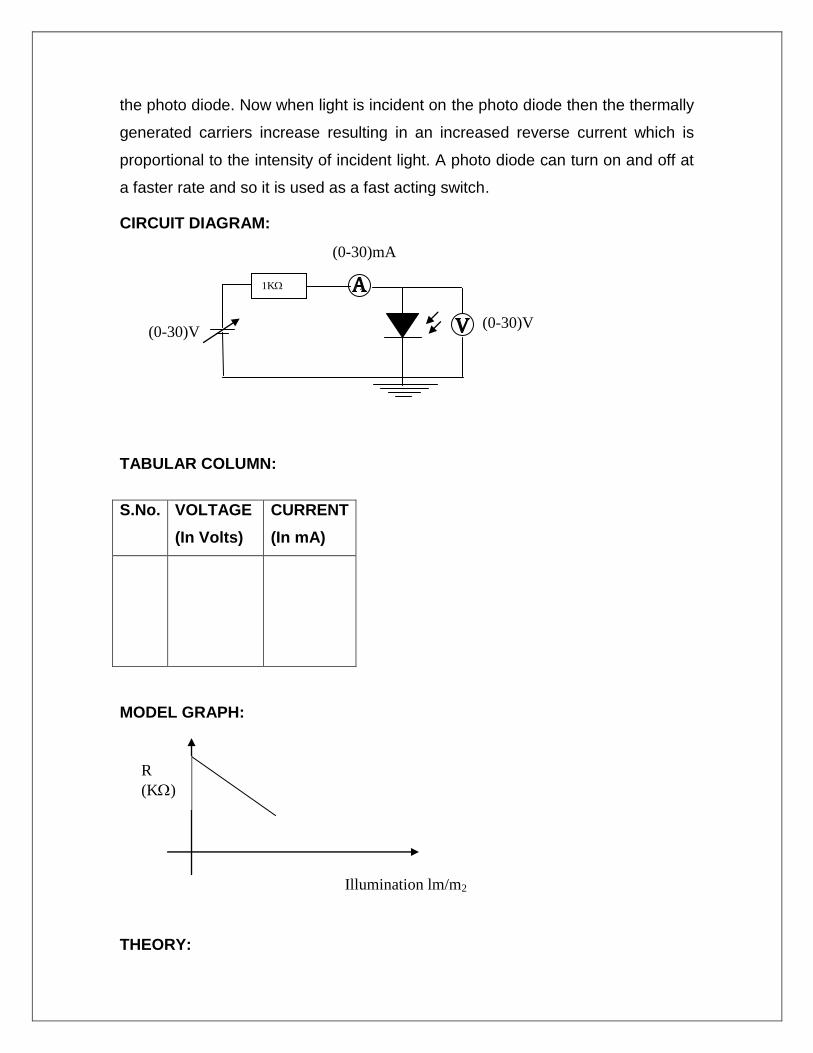
(0-30)mA
(0-30)V (0-30)V
the photo diode. Now when light is incident on the photo diode then the thermally
generated carriers increase resulting in an increased reverse current which is
proportional to the intensity of incident light. A photo diode can turn on and off at
a faster rate and so it is used as a fast acting switch.
CIRCUIT DIAGRAM:
TABULAR COLUMN:
MODEL GRAPH:
THEORY:
S.No. VOLTAGE
(In Volts)
CURRENT
(In mA)
R
(K)
Illumination lm/m2
1K a
a
a
a
a
A
A
A

IC
PHOTOTRANSISTOR:
It is a transistor with an open base; there exists a small collector current
consisting of thermally produced minority carriers and surface leakage. By
exposing the collector junction to light, a manufacturer can produce a
phototransistor, a transistor that has more sensitivity to light than a photo diode.
Because the base lead is open, all the reverse current is forced into the base of
the transistor. The resulting collector current is ICeo = dcIr. The main difference
between a phototransistor and a photodiode is the current gain, dc. The same
amount of light striking both devices produces dc times more current in a
phototransistor than in a photodiode.
CIRCUIT DIAGRAM:
TABULAR COLUMN: SYMBOL:
E
MODEL GRAPH:
S. No. VCE
(in Volts)
IC
(in mA)
N P N
1K
(0-30V)
C
(mA)

400 Lux
200 Lux
0 Lux
VCE(V)
PROCEDURE:
PHOTO DIODE:
16. Rig up the circuit as per the circuit diagram.
17. Maintain a known distance (say 5 cm) between the DC bulb and
the photo diode.
18. Set the voltage of the bulb (say, 2V), vary the voltage of the diode
insteps of 1V and note down the corresponding diode current, Ir.
19. Repeat the above procedure for the various voltages of DC bulb.
20. Plot the graph: VD vs. Ir for a constant DC bulb voltage.
PHOTOTRANSISTOR:
16. Rig up the circuit as per the circuit diagram.
17. Maintain a known distance (say 5 cm) between the DC bulb and the
phototransistor.
18. Set the voltage of the bulb (say, 2V), vary the voltage of the diode
in steps of 1V and note down the corresponding diode current, Ir.
19. Repeat the above procedure for the various values of DC bulb.
20. Plot the graph: VD vs. Ir for a constant bulb voltage.
RESULT:
Thus the characteristics of photo diode and phototransistor are studied.
Ex.No.6
CHARACTERISTICS OF THERMISTOR
AIM:
To study the characteristics of Thermistor.
THEORY:
Thermistor or Thermal resistor is two – terminal semiconductor device
whose resistance is temperature sensitive. The value of such resistors decreases
with increase in temperature. Materials employed in the manufacture of the
thermistors include oxides of cobalt, nickel, copper, iron uranium and
manganese.
The thermistors has very high temperature coefficient of resistance, of the
order of 3 to 5% per C, making it an ideal temperature transducer. The
temperature coefficient of resistance is normally negative. The reistance at any
temperature T, is given approximately by
RT = Ro exp β (1/T – 1/To)
Where RT = thermistor resistance at temperature T (K), RO = thersmistor
resistance at temperature To (K), and = a constant determined by calibration.
At high temperatures, this equation reduces to
RT = Ro exp ( β/T)
The resistance – temperature characteristics is shown in Fig 21.10. The
curve is non – linear and the drop in resistance from 5000 to 10 occurs for an
increase in temperature from 20 to 100 C. The temperature of the device can
be changed internally or externally. An increase in current through the device will
raise its temperature carrying a drop in its terminal resistance. Any externally
heat source will result in an increase in its body temperature and drop in

resistance this type action (internal or external) lends itself well to control
mechanism.
Three useful parameters for characterizing the thermistor are the time
constant, dissipation constant , and resistance ratio. The time constant is the
time for a thermistor to change its resistance by 63% of its initial value, for zero –
power dissipation. Typical values of time constant range from 1 to 50 s.
SYMBOL:
MODEL GRAPH:
The dissipation factor is the power necessary to increase the temperature
of a thermistor by 1˚C. Typical values of dissipation factor range from 1 to 10
mW/˚C.
Resistance ratio is the ratio of the resistance at 25 ˚C. Its range is
approximately
3 – 60.
R
(-cm)
T (deg)
T

Thermistors are used measure temperature, flow pressure, liquid level,
voltage or power level, vacuum, composition of gases and thermal conductivity
and also in compensation network.
RESULT:
Thus the Characteristics of thermistor was studied.

Ex.No.7a
SINGLE PHASE HALF WAVE RECTIFIER
AIM:
To construct a Half wave rectifier using diode and to draw its performance
characteristics.
APPARATUS REQUIRED: COMPONENTS
REQUIRED:
S.
No. Name Range Type Qty
S.
No. Name Range Type Qty
1 Transformer 230/(6-0-6)V 1 1
Diode IN4001 1
2 R.P.S (0-30)V 2
3 Ammeter
(0–30)mA 1 2 Resistor 1K 1
(0–250)µA 1 3 Bread
Board
1
4 Voltmeter (0–30)V 1 4 Capacitor 100µf 1
(0–2)V 1 5 CRO 1
FORMULAE:
WITHOUT FILTER:
(i) Vrms = Vm / 2
(ii) Vdc = Vm /
(iii) Ripple Factor = (Vrms / Vdc)2 – 1
(iv) Efficiency = (Vdc / Vrms)2 x 100
WITH FILTER:
(i) Vrms = (Vrms’2 + Vdc
2)
(ii) Vrms’ = Vrpp / (3 x 2)
(iii) Vdc = Vm – V rpp / 2
(iv) Ripple Factor = Vrms’/ Vdc
PROCEDURE:

WITHOUT FILTER:
13. Give the connections as per the circuit diagram.
14. Give 230v, 50HZ I/P to the step down TFR where secondary connected to
the Rectifier I/P.
15. Take the rectifier output across the Load.
16. Plot its performance graph.
WITH FILTER:
1. Give the connections as per the circuit diagram.
14. Give 230v, 50HZ I/P to the step down TFR where secondary connected to
the Rectifier I/P.
15. Connect the Capacitor across the Load.
16. Take the rectifier output across the Load.
17. Plot its performance graph.
CIRCUIT DIAGRAM:
1 Transformer
230 V / 6V 1N 4007
1K 100F 1, 230V,
50Hz
AC supply
CRO

TABULAR COLUMN:
WITHOUT FILTER:
Vm Vrms Vdc Ripple factor Efficiency
WITH FILTER:
Vrms Vrpp Vdc Ripple factor Efficiency
MODEL GRAPH:
RESULT:
Thus the performance characteristics of 1 Half wave rectifier was obtained.
Ex.No.7b
Vin
(Volts)
t (ms)
Vo
(Volts)
t (ms)
t (ms)
Vo
(Volts)
Without Filter
With Filter

SINGLE PHASE FULL WAVE RECTIFIER
AIM:
To construct a Full wave rectifier using diode and to draw its performance
characteristics.
APPARATUS REQUIRED: COMPONENTS
REQUIRED:
S.
No. Name Range Type Qty
S.
No. Name Range Type Qty
1 Transformer 230/(6-0-6)V 1 1
Diode IN4001 2
2 R.P.S (0-30)V 2
3 Ammeter
(0–30)mA 1 2 Resistor 1K 1
(0–250)µA 1 3 Bread
Board
1
4 Voltmeter (0–30)V 1 4 Capacitor 100µf 1
(0–2)V 1 5 CRO 1
FORMULAE:
WITHOUT FILTER:
(i) Vrms = Vm / 2
(ii) Vdc = 2Vm /
(iii) Ripple Factor = (Vrms / Vdc)2 – 1
(iv) Efficiency = (Vdc / Vrms)2 x 100
WITH FILTER:
(i) Vrms = Vrpp /(2* 3)
(ii) Vdc = Vm – V rpp
(iv) Ripple Factor = Vrms’/ Vdc
PROCEDURE:
WITHOUT FILTER:
13. Give the connections as per the circuit diagram.
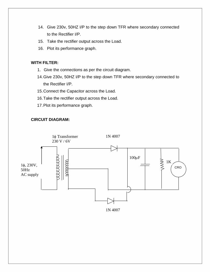
14. Give 230v, 50HZ I/P to the step down TFR where secondary connected
to the Rectifier I/P.
15. Take the rectifier output across the Load.
16. Plot its performance graph.
WITH FILTER:
1. Give the connections as per the circuit diagram.
14. Give 230v, 50HZ I/P to the step down TFR where secondary connected to
the Rectifier I/P.
15. Connect the Capacitor across the Load.
16. Take the rectifier output across the Load.
17. Plot its performance graph.
CIRCUIT DIAGRAM:
1N 4007
1K 100F
1, 230V,
50Hz
AC supply
CRO
1N 4007
1 Transformer
230 V / 6V
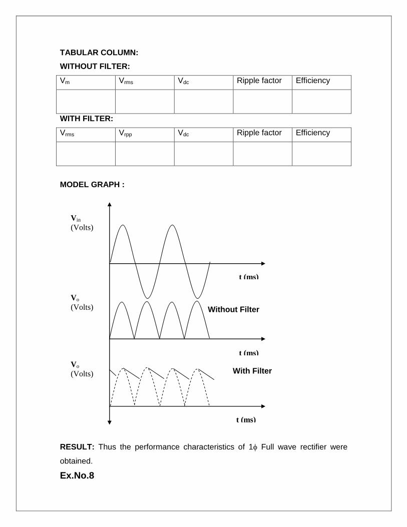
TABULAR COLUMN:
WITHOUT FILTER:
Vm Vrms Vdc Ripple factor Efficiency
WITH FILTER:
Vrms Vrpp Vdc Ripple factor Efficiency
MODEL GRAPH :
RESULT: Thus the performance characteristics of 1 Full wave rectifier were
obtained.
Ex.No.8
Vin
(Volts)
t (ms)
Vo
(Volts)
t (ms)
t (ms)
Vo
(Volts)
Without Filter
With Filter

DIFFERENTIAL AMPLIFIER
AIM:
To construct a Differential amplifier in Common mode & Differential mode
configuration and to find common mode rejection ratio.
APPARATUS REQUIRED: COMPONENTS REQUIRED:
Apparatus Range Qty
1 RPS (0-30)V 1
2 CRO 1
3 Signal
Generator 1
4 DCB 2
5 DRB 2
THEORY:
The Differential amplifier circuit is an extremely popular connection used in
IC units. The circuit has separate inputs , two separate outputs and emitters are
connected together. If the same input is applied to both inputs, the operation is
called common mode. In double ended operation two input signals are applied ,
the difference of the inputs resulting in outputs from both collectors due to the
difference of the signals applied to both the inputs. The main feature of the
differential amplifier is the very large gain when opposite signals are applied to
inputs as compared to small signal resulting from common input. The ratio of this
difference gain to the common gain is called common mode rejection ratio.
CIRCUIT DIAGRAM:
DIFFERENTIAL MODE:
S.No Item Type Range Qty
1 Transistor BC107 1
2 Capacitor 470F 1
3 Resistor 3.9KΩ
3.3KΩ
1
1
4 Bread board 1

COMMON MODE:
9V
3.3 K
3.9K
Vo1 Vo2
V2
13V
3.9K
-9V
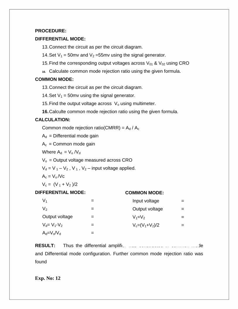
PROCEDURE:
DIFFERENTIAL MODE:
13. Connect the circuit as per the circuit diagram.
14. Set V1 = 50mv and V2 =55mv using the signal generator.
15. Find the corresponding output voltages across V01 & V02 using CRO
16. Calculate common mode rejection ratio using the given formula.
COMMON MODE:
13. Connect the circuit as per the circuit diagram.
14. Set V1 = 50mv using the signal generator.
15. Find the output voltage across Vo using multimeter.
16. Calculte common mode rejection ratio using the given formula.
CALCULATION:
Common mode rejection ratio(CMRR) = Ad / Ac
Ad = Differential mode gain
Ac = Common mode gain
Where Ad = Vo /Vd
Vo = Output voltage measured across CRO
Vd = V 1 – V2 , V 1 , V2 – input voltage applied.
Ac = Vo /Vc
Vc = (V 1 + V2 )/2
DIFFERENTIAL MODE:
V1 =
V2 =
Output voltage =
Vd= V1-V2 =
Ad=Vo/Vd =
RESULT: Thus the differential amplifier was constructed in common mode
and Differential mode configuration. Further common mode rejection ratio was
found
Exp. No: 12
COMMON MODE:
Input voltage =
Output voltage =
V1=V2 =
Vc=(V1+V2)/2 =

PASSIVE FILTERS
Aim:
To attenuate unwanted frequency components from input signal by using resistor
and capacitor.
Apparatus required:
S.No Name of the apparatus Range Type Quantity
1. Signal Generator 01
2. Resistor 01
3. Capacitor Ceramic 01
4. CRO 01
5. Breadboard 01
Theory:
A filter is an AC circuit that separates some frequencies from other in
within mixed – frequency signals. Audio equalizers and crossover networks are
two well-known applications of filter circuits. A Bode plot is a graph plotting
waveform amplitude or phase on one axis and frequency on the other.
A low-pass filter allows for easy passage of low-frequency signals from
source to load, and difficult passage of high-frequency signals. Capacitor low-pass
filters insert a resistor in series and a capacitor in parallel with the load as shown
in the circuit diagram. The former filter design tries to “block” the unwanted
frequency signal while the latter tries to short it out.
The cutoff frequency for a low-pass filter is that frequency at which the
output (load) voltage equals 70.7% of the input (Source) voltage. Above the cutoff
frequency, the output voltage is lower than 70.7% of the input, and vice-versa. See
the circuit diagram
1
Fcutoff = ----------

2RC
A high-pass filter allows for easy passage of high-frequency signals from source to
load, and difficult passage of low-frequency signals. Capacitor high-pass filters
insert a capacitor in series with the load as shown in the circuit diagram. The
former filter design tries to “brick” the unwanted frequency signal while the latter
tries to short it out.
The cutoff frequency for a high-pass filter is that frequency at which the
output (load) voltage equals 70.7% of the input (source) voltage. Above the cutoff
frequency, the output voltage is greater than 70.7% of the input, and vice-versa.
1
Fcutoff = ----------
2RC
A band – pass filter works to screen out frequencies that are too low or too
high, giving easy passage only to frequencies within a certain range. Stacking a
low-pass filter on the end of a high-pass filter, or vice-versa can make band-pass
filters. Refer the circuit diagrams
Fig. 7.6
“Attenuate” means to reduce or diminish in amplitude. When you
turn down the volume control on your stereo, you are “attenuating” the signal
being sent to the speakers.
A band-stop filter works to screen out frequencies that are within a certain
range, giving easy passage only to frequencies outside of that range. Also known
as band-elimination, band-reject, or notch filters.
Placing a low-pass filter in parallel with a high-pass filter can make band-
stop filters. Commonly, both the low-pass and high-pass filter sections are of the
Signal
input
Low-pass filter High-pass filter Signal
output Blocks frequencies
that are too high
Blocks frequencies
that are too low

Signal
Input
Low-pass filter
High-pass filter
Signal
Output
“T” configuration giving the name “Twin-T” to the band-stop combination. Refer
the fig.7.7, 7.8a and 7.8b.
Passes low frequencies
Passes high frequencies
Fig. 7.8a
The frequency of maximum attenuation is called the notch
frequency.
Procedure:
19. Give the connections as per circuit diagrams.
20. Switch on the main.
21. Change the frequency from minimum and find the output
voltage by using CRO.
22. Draw the graph.
23. Verify the cut off frequency.
24. Switch off the main.
Result:
Thus we analyze passive filter and various waveforms are noted
Exp. No : 10
STUDY OF CRO AND
POWER FACTOR MEASUREMENT USING CRO
Aim:
To study cathode Ray Oscilloscope (CRO) and measurement of power factor using
CRO.

Apparatus required:
S.No Name of the apparatus Range Type Quantity
1. Resistance Box 1
2. Capacitance Box 1
3. Inductance Box 1
4. Function Generator 1
5. Bread board 1
Theory:
The cathode ray oscilloscope is the most versatile measuring instrument
available. We can measure following parameters using the CRO:
13. AC or DC voltage.
14. Time (t=1/f).
15. Phase relationship
16. Waveform calculation: Rise time; fall time; on time; off-time
Distortion, etc.
We can also measure non-electrical physical quantities like pressure, strain,
temperature, acceleration, etc., by converting into electrical quantities using
a transducer.
Major blocks:
19. Cathode ray tube (CRT)
20. Vertical amplifier
21. Horizontal amplifier
22. Sweep generator
23. Trigger circuit
24. Associated power supply.

16. The cathode ray tube is the heart of CRO. The CRT is enclosed in an
evacuated glass envelope to permit the electron beam to traverse in the
tube easily. The main functional units of CRO are as follows.
Electron gun assembly
Deflection plate unit
Screen.
17. Vertical Amplifier is the main factor in determining the bandwidth and
sensitivity of an oscilloscope. Vertical sensitivity is a measure of how
much the electron beam will be deflected for a specified input signal.
On the front panel of the oscilloscope, one can see a knob attached to a
rotary switch labeled volts/division. The rotary switch is electrically
connected to the input attenuation network. The setting of the rotary
switch indicates what amplitude signal is required to deflect the beam
vertically by one division.
18. Horizontal amplifier Under normal mode of operation, the horizontal
amplifier will amplify the sweep generator input. When the CRO is
being used in the X-Y mode, the horizontal amplifier will amplify the
signal applied to the horizontal input terminal. Although the vertical
amplifier mush be able to faithfully reproduce low-amplitude and high
frequency signal with fast rise-time, the horizontal amplifier is only
required to provide a faithful reproduction of the sweep signal which
has a relatively high amplitude and slow rise time.
19. Sweep generator and Trigger circuit These two units form the Signal
Synchronization unit of the CRO.
20. Associated Power Supply: The input signal may come from an
external source when the trigger selector switch is set to EXT or from
low amplitude AC voltage at line frequency when the switch is set to
LINE or from the vertical amplifier when the switch is set to INT. When
set for INT (internal triggering), the trigger circuit receives its inputs
from the vertical amplifier.

Major Blocks in a Practical CRO
A CRO consists of a cathode ray tube (CRT) and additional control knobs.
The main parts of a CRT are:
10. Electron gun assembly.
11. Deflection plate assembly.
12. Fluorescent screen.
Electron Gun Assembly: The electron gun assembly produces a sharp beam of
electrons, which are accelerated to high velocity. This focused beam of electrons
strike the fluorescent screen with sufficient energy to cause a luminous spot on the
screen.
Deflection plate assembly: This part consists of two plates in which one pair of
plates is placed horizontally and other of plates is placed vertically. The signal
under test is applied to vertical deflecting plates. The horizontal deflection plates
are connected to a built-in ramp generator, which moves the luminous spot
periodically in a horizontal direction from left to right over the screen. These two
deflection plates give stationary appearance to the waveform on the screen. CRO
operates on voltage. Since the deflection of the electron beam is directly
proportional to the deflecting voltage, the CRT may be used as a linear measuring
device. The voltage being measured is applied to the vertical plates through an
iterative network, whose propagation time corresponds to the velocity of electrons,
thereby synchronizing the voltage applied to the vertical plate with the velocity of
the beam.

Synchronization of input signal: The sweep generator produces a saw tooth
waveform, which is used to synchronize the applied voltage to obtain a stationary-
applied signal. This requires that the time base be operated at a submultiples
frequency of the signal under measurement. If synchronization is not done, the
pattern is not stationary, but appears to drift across the screen in a random fashion.
Internal synchronization This trigger is obtained from the time base generator to
synchronize the signal.
External synchronization An external trigger source can also be used to
synchronize the signal being measured.
Auto Triggering Mode The time base used in this case in a self-oscillating
condition, i.e., it gives an output even in the absence of any Y-input. The
advantage of this mode is that the beam is visible on the screen under all
conditions, including the zero input. When the input exceeds a certain magnitude
then the internal free running oscillator locks on to the frequency.
Precautions:
7. The ammeter is connected using thick wires.
8. While reversing ammeter polarity, see to it that the capacitor is not
discharged.
Observation:
Sl.No Time Voltage Current
Unit (Sec) (Volts) (Amps)
Result: Thus we study about CRO & to measure p.f