lecture 4. self-assembled monolayers...
TRANSCRIPT
Self-assembly and Nanotechnology 10.524
Lecture 4. Self-assembled Monolayers (SAM)
Instructor: Prof. Zhiyong Gu (Chemical Engineering& UML CHN/NCOE Nanomanufacturing Center)
Self-assembly and Nanotechnology

Lecture 4: Self-assembled Monolayers (SAMs)
Table of Contents
Definition of SAMs
Str ct res & PropertiesStructures & Properties
Applications, including SAMs for nanofabrication andt h lnanotechnology
Case study: micro-contact printing
Self-assembly and Nanotechnology

Lecture 4: Self-assembled Monolayers (SAMs)
Self-Assembled Monolayers
Figure Number of published articles dealing with self assembledFigure. Number of published articles dealing with self-assembledmonolayers per year, according to searches in the Chemical Abstracts and Science Citation Index databases
Self-assembly and Nanotechnology

Lecture 4: Self-assembled Monolayers (SAMs)
D fi iti f lDefinition of monolayers
“SAMs are ordered molecular assemblies formed by the adsorption of an active surfactant on a solid surface” (or other surfaces such as liquid)
Self-assembly and Nanotechnology
Abraham Ulman, Chem. Rev. 1996, 96, 1533-1554
Lecture 4: Self-assembled Monolayers (SAMs)
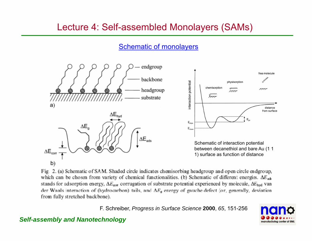
S h ti f lSchematic of monolayers
Schematic of interaction potential between decanethiol and bare Au (1 1 1) surface as function of distance
Self-assembly and Nanotechnology
F. Schreiber, Progress in Surface Science 2000, 65, 151-256
Lecture 4: Self-assembled Monolayers (SAMs)
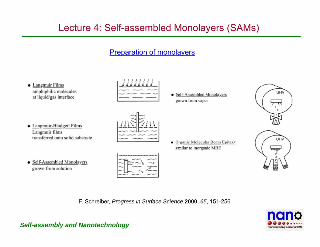
Preparation of monolayers
F Schreiber Progress in Surface Science 2000 65 151 256
Self-assembly and Nanotechnology
F. Schreiber, Progress in Surface Science 2000, 65, 151-256

Lecture 4: Self-assembled Monolayers (SAMs)
From solution: immersion technique
Self-assembly and Nanotechnology
Abraham Ulman, Chem. Rev. 1996, 96, 1533-1554

Lecture 4: Self-assembled Monolayers (SAMs)
Some frequentlyused monolayersy
Self-assembly and NanotechnologyF. Schreiber, Progress in Surface Science 2000, 65, 151-256
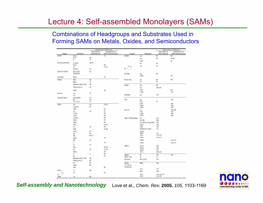
Lecture 4: Self-assembled Monolayers (SAMs)Combinations of Headgroups and Substrates Used in Forming SAMs on Metals, Oxides, and Semiconductors
Self-assembly and Nanotechnology Love et al., Chem. Rev. 2005, 105, 1103-1169
Lecture 4: Self-assembled Monolayers (SAMs)
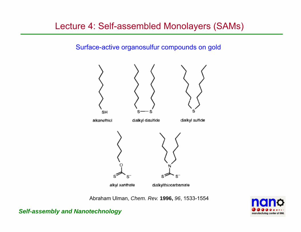
Surface-active organosulfur compounds on gold
Self-assembly and Nanotechnology
Abraham Ulman, Chem. Rev. 1996, 96, 1533-1554
Lecture 4: Self-assembled Monolayers (SAMs)
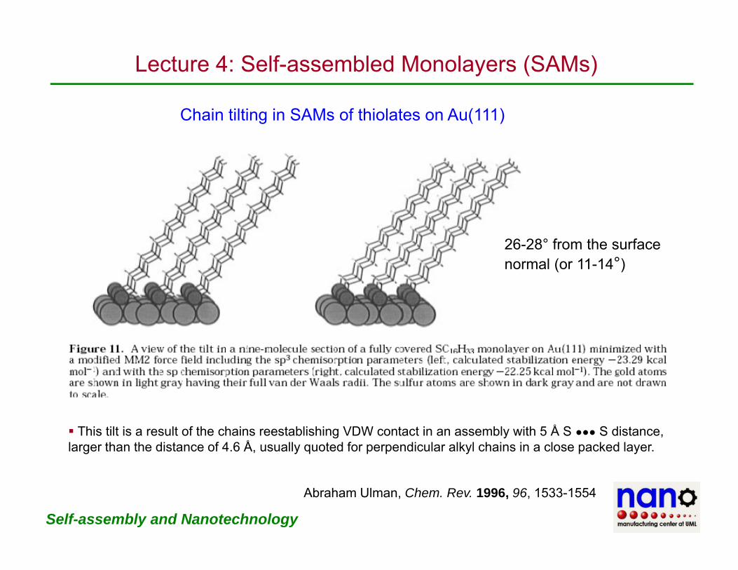
Chain tilting in SAMs of thiolates on Au(111)
26-28° from the surface26 28 from the surface normal (or 11-14°)
This tilt is a result of the chains reestablishing VDW contact in an assembly with 5 Å S ●●● S distance, larger than the distance of 4.6 Å, usually quoted for perpendicular alkyl chains in a close packed layer.
Self-assembly and Nanotechnology
Abraham Ulman, Chem. Rev. 1996, 96, 1533-1554
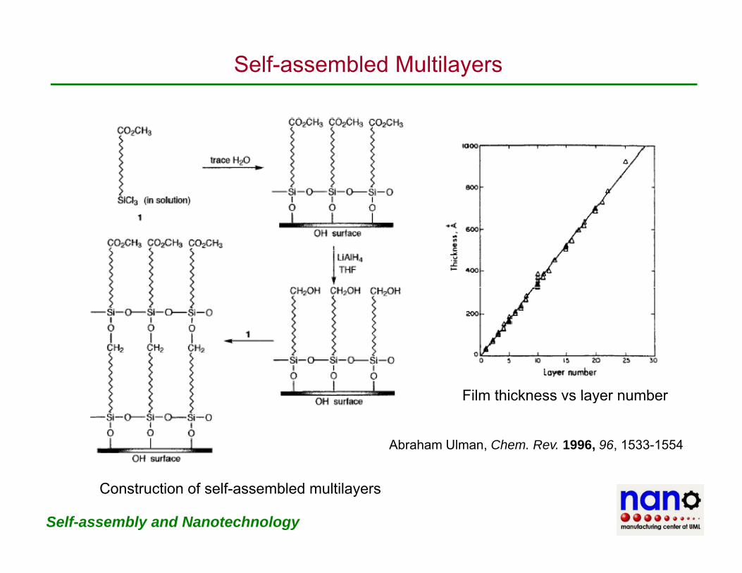
Self-assembled Multilayers
Film thickness vs layer numberFilm thickness vs layer number
Abraham Ulman, Chem. Rev. 1996, 96, 1533-1554
Self-assembly and Nanotechnology
Construction of self-assembled multilayers
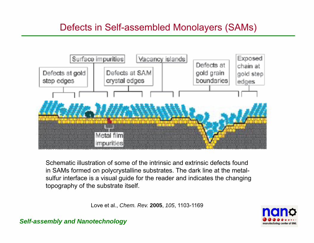
Defects in Self-assembled Monolayers (SAMs)
Schematic illustration of some of the intrinsic and extrinsic defects found in SAMs formed on polycrystalline substrates. The dark line at the metal-sulfur interface is a visual guide for the reader and indicates the changing topography of the substrate itself.
Self-assembly and Nanotechnology
Love et al., Chem. Rev. 2005, 105, 1103-1169

Scanning Probe Lithography Nanofabrication of SAMs
Schematic diagrams of four basic manipulation mechanisms using AFM (A and B) and STM (C and D). The imaging and fabrication modes are depicted in the top and bottom rows, respectively.
Self-assembly and Nanotechnology
Liu, Xu, Qian. Acc. Chem. Res. 2000, 33, 457-466

Scanning Probe Lithography Nanofabrication of SAMs
(A) 160-160 nm2 topographic images of C18S/Au(111) with the thiols shaved away from the central 50-50 nm2 square.(B) 160-160 nm2 topographic images of(B) 160-160 nm2 topographic images of OTE/mica containing a heart-shaped pattern produced using nanoshaving.
(A) Fabrication of two C18S nanoislands (3 - 5 and 50-50 nm2) in the matrix of a C10S monolayer using nanografting.nanografting.
(C) Fabrication of multicomponent patterns using nanografting.
Self-assembly and Nanotechnology
Liu, Xu, Qian. Acc. Chem. Res. 2000, 33, 457-466

Sensing and Proteins Binding on SAMs-modified Electrodes
Electrochemical sensing by SAMs modified electrodes
Electrochemical studies of proteins onSAMs-modified electrodes
Cyclic voltammogram of Au electrode modified with 17-mer peptide in the absence and presence of cAMP
Reversible formation of a protein triple layer on SAM using biotinylated alkylthiols
Self-assembly and Nanotechnology
absence and presence of cAMP y g y y
Dojindo Molecular Technologies, Inc.
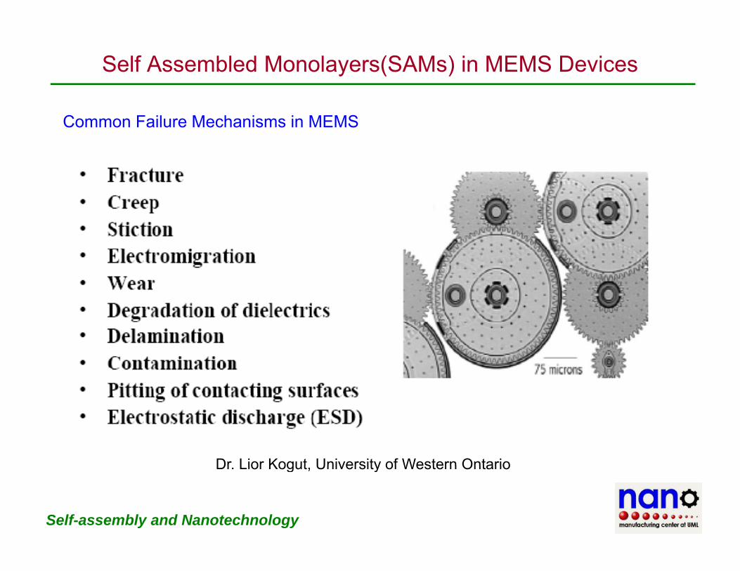
Self Assembled Monolayers(SAMs) in MEMS Devices
Common Failure Mechanisms in MEMS
Dr Lior Kogut University of Western Ontario
Self-assembly and Nanotechnology
Dr. Lior Kogut, University of Western Ontario

Self Assembled Monolayers(SAMs) in MEMS Devices
Advnatages of SAMs in MEMS
(a) Eliminate release stiction by effectively reversing the shape of the water meniscus;water meniscus;
(b) Reduce in-use stiction by three to four orders of magnitude with respect to the conventional oxidized release process;
(c) Eliminate the need for large input signals or mechanical probing in the start-up phase in microengines;
(d) Reduce friction in microengines static friction value of 0.08 vs. 2.3 f id t d ffor oxide-coated surfaces;
(e) Reduce wear significantly over 40 million operation cycles have been achieved in touch-mode electrostatic actuators;
(f) Survive packaging environments thermally stable to 4000C in various, including oxygen containing, environments.
Self-assembly and Nanotechnology
Dr. Lior Kogut, University of Western Ontario
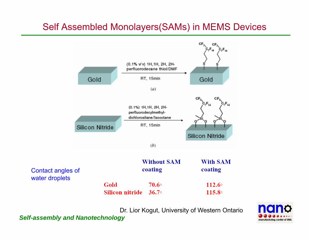
Self Assembled Monolayers(SAMs) in MEMS Devices
Contact angles of water droplets
Self-assembly and NanotechnologyDr. Lior Kogut, University of Western Ontario

Self Assembled Monolayers (SAMs) in MEMS Devices
Self-assembly and NanotechnologyDr. Lior Kogut, University of Western Ontario
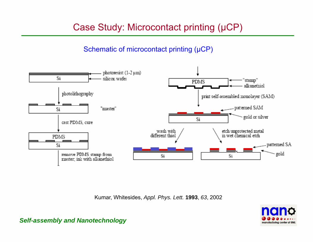
Case Study: Microcontact printing (µCP)
Schematic of microcontact printing (µCP)
Kumar Whitesides Appl Phys Lett 1993 63 2002
Self-assembly and Nanotechnology
Kumar, Whitesides, Appl. Phys. Lett. 1993, 63, 2002
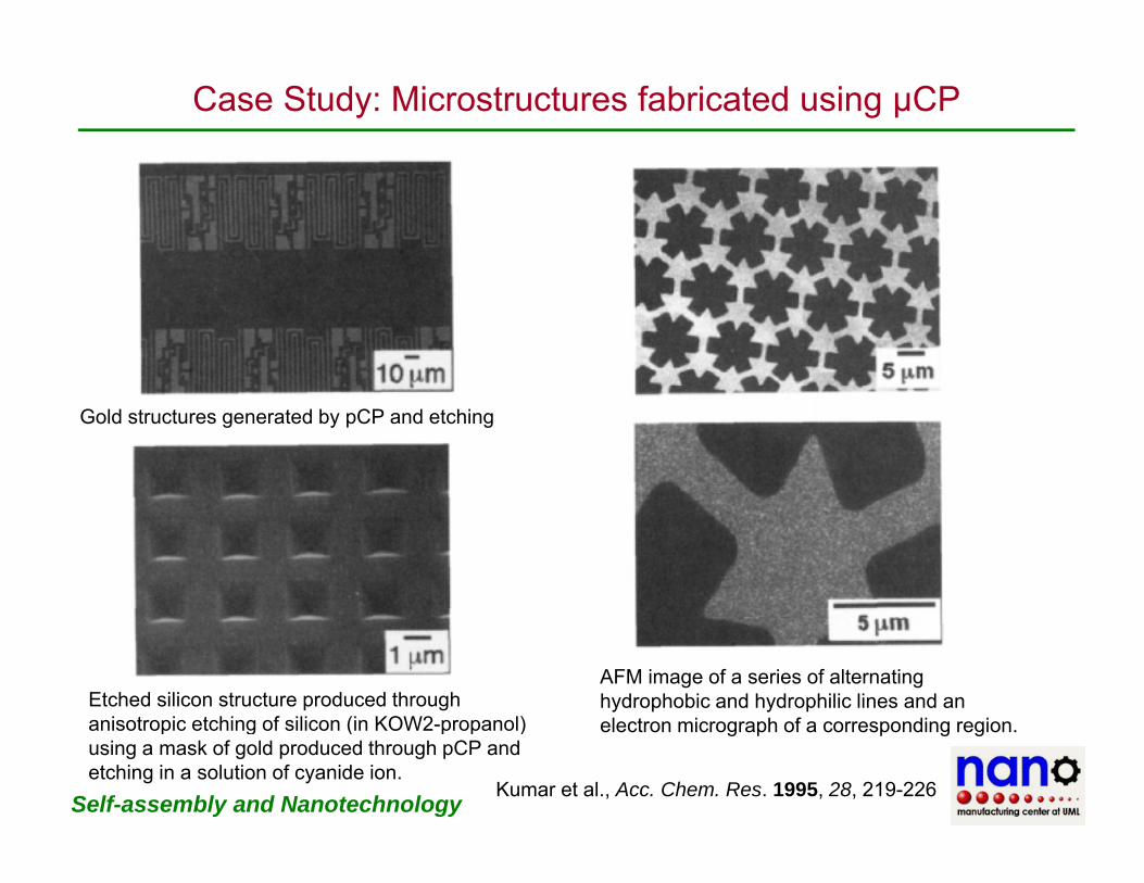
Case Study: Microstructures fabricated using µCP
Gold structures generated by pCP and etching
Etched silicon structure produced through anisotropic etching of silicon (in KOW2 propanol)
AFM image of a series of alternating hydrophobic and hydrophilic lines and an
l t i h f di i
Self-assembly and Nanotechnology
anisotropic etching of silicon (in KOW2-propanol) using a mask of gold produced through pCP and etching in a solution of cyanide ion.
electron micrograph of a corresponding region.
Kumar et al., Acc. Chem. Res. 1995, 28, 219-226

Case Study: Microstructures fabricated using µCP
Self-assembly and Nanotechnology