lecture 12 latches section 5.1-5.3, 9.1-9.2. block diagram of sequential circuit gates new output is...
TRANSCRIPT
Lecture 12
Latches Section 5.1-5.3, 9.1-9.2

Block Diagram of Sequential Circuit
gates
New output is dependent on the inputs and the preceding values of outputs.Characteristic: the output node is intentionally connected back to inputs.
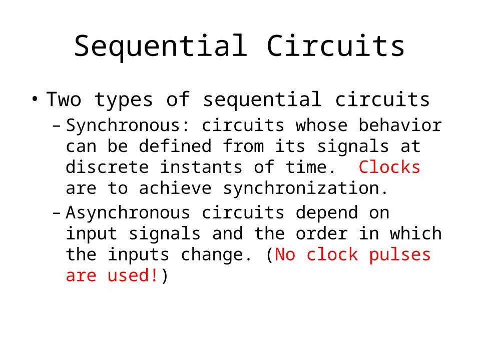
Sequential Circuits
• Two types of sequential circuits– Synchronous: circuits whose behavior
can be defined from its signals at discrete instants of time. Clocks are to achieve synchronization.
– Asynchronous circuits depend on input signals and the order in which the inputs change. (No clock pulses are used!)
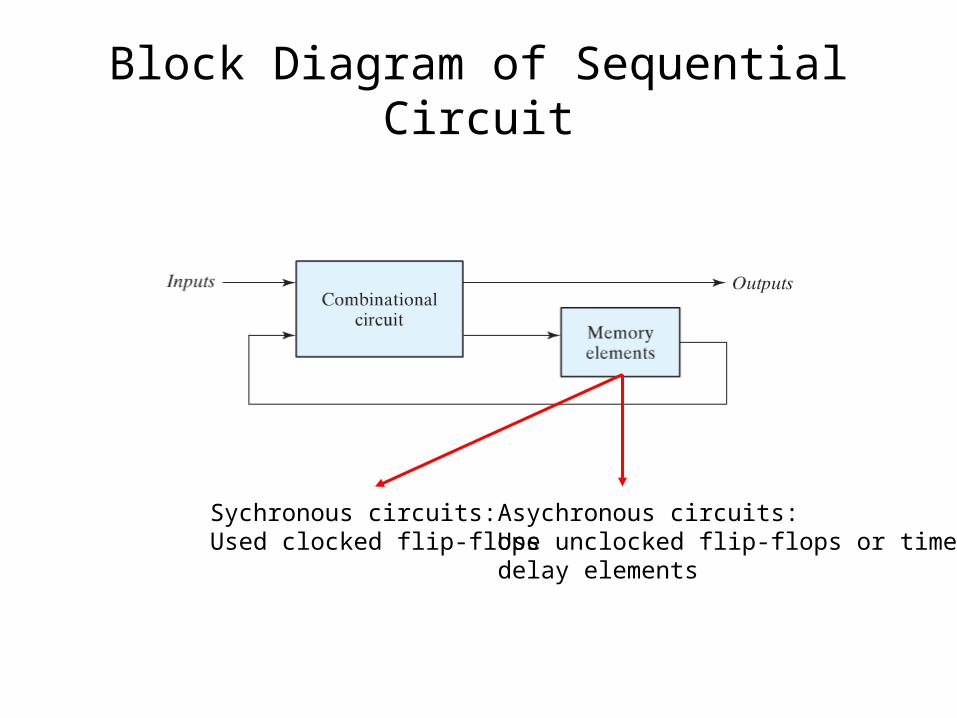
Block Diagram of Sequential Circuit
Sychronous circuits:Used clocked flip-flops
Asychronous circuits:Use unclocked flip-flops or time delay elements

Applications of Asynchronous Circuits
• Asynchronous circuits are important where the digital system must respond quickly without having to wait for a clock pulse
• Useful in small independent circuits that require only a few components—where it may not be practical to go to the expense of providing a circuit for generating clock pulses!
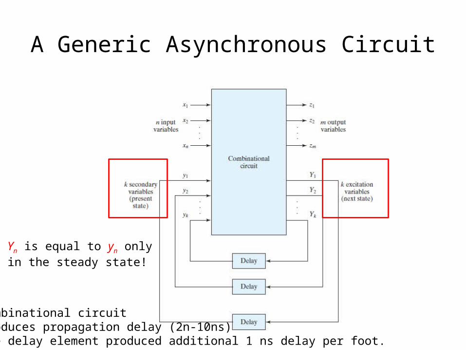
A Generic Asynchronous Circuit
Yn is equal to yn onlyin the steady state!
Combinational circuitproduces propagation delay (2n-10ns)The delay element produced additional 1 ns delay per foot.
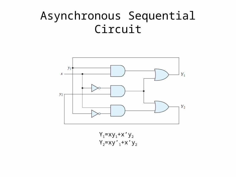
Asynchronous Sequential Circuit
Y1=xy1+x’y2
Y2=xy’1+x’y2
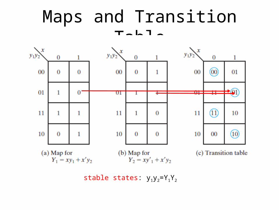
Maps and Transition Table
stable states: y1y2=Y1Y2

Toggle x
X= 0→1 → 0 → 1
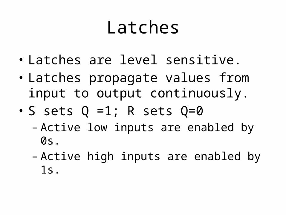
Latches
• Latches are level sensitive.• Latches propagate values from input
to output continuously.• S sets Q =1; R sets Q=0– Active low inputs are enabled by 0s.– Active high inputs are enabled by 1s.
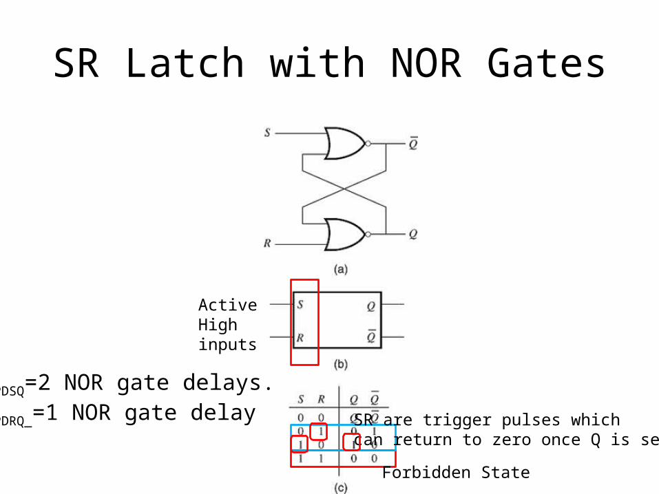
SR Latch with NOR Gates
tPDSQ=2 NOR gate delays.tPDRQ_=1 NOR gate delay
Forbidden State
SR are trigger pulses which can return to zero once Q is set.
Active High inputs
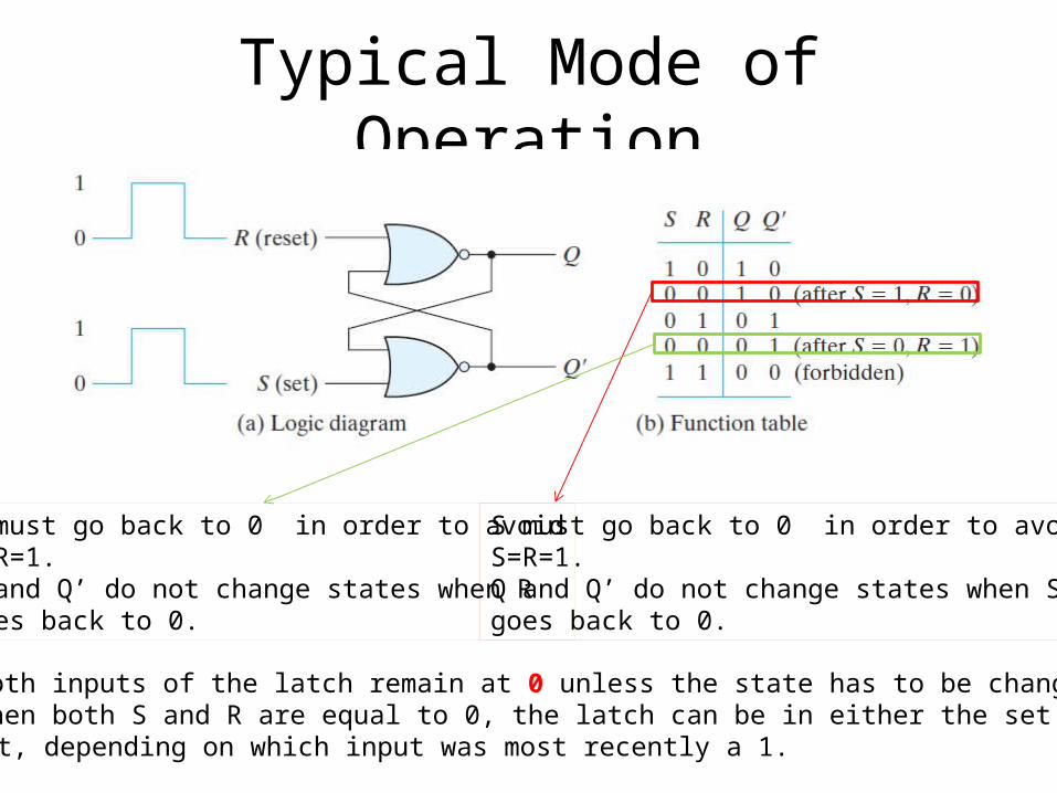
Typical Mode of Operation
1. Both inputs of the latch remain at 0 unless the state has to be changed.2. When both S and R are equal to 0, the latch can be in either the set or the reset, depending on which input was most recently a 1.
S must go back to 0 in order to avoidS=R=1.Q and Q’ do not change states when Sgoes back to 0.
R must go back to 0 in order to avoidS=R=1.Q and Q’ do not change states when Rgoes back to 0.
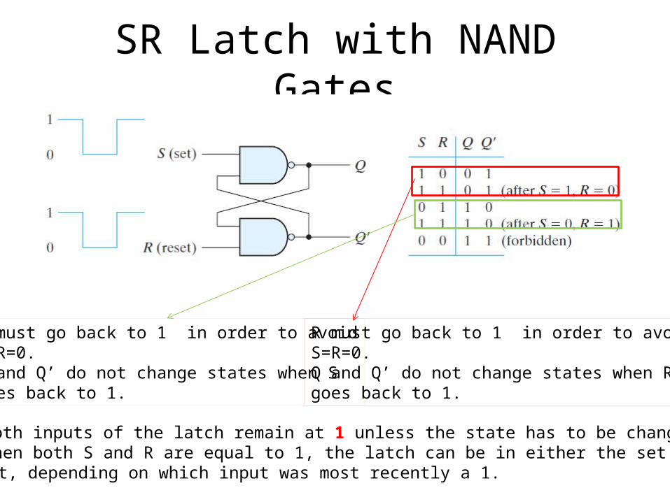
SR Latch with NAND Gates
1. Both inputs of the latch remain at 1 unless the state has to be changed.2. When both S and R are equal to 1, the latch can be in either the set or the reset, depending on which input was most recently a 1.
R must go back to 1 in order to avoidS=R=0.Q and Q’ do not change states when Rgoes back to 1.
S must go back to 1 in order to avoidS=R=0.Q and Q’ do not change states when Sgoes back to 1.
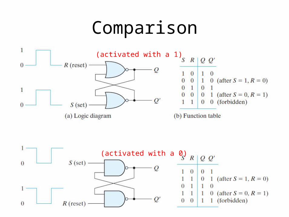
Comparison(activated with a 1)
(activated with a 0)
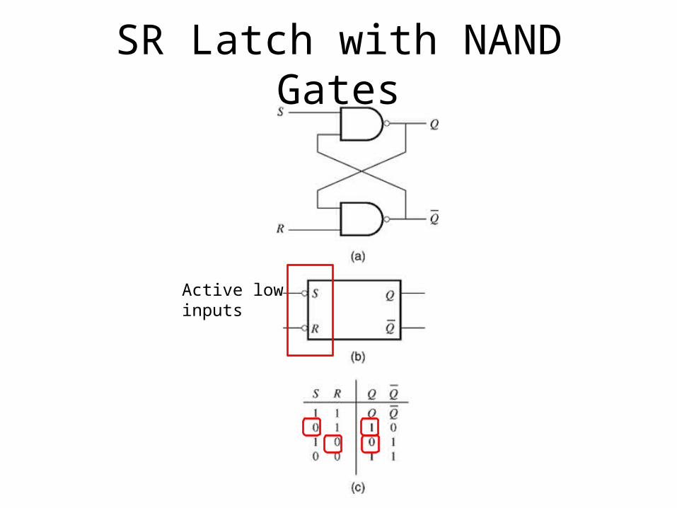
SR Latch with NAND Gates
Active lowinputs
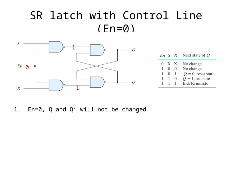
SR latch with Control Line (En=0)
1. En=0, Q and Q’ will not be changed!
0
1
1
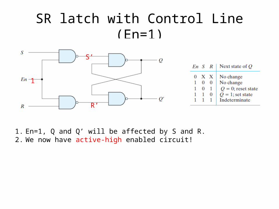
SR latch with Control Line (En=1)
1. En=1, Q and Q’ will be affected by S and R.2. We now have active-high enabled circuit!
1
S’
R’

D Latch
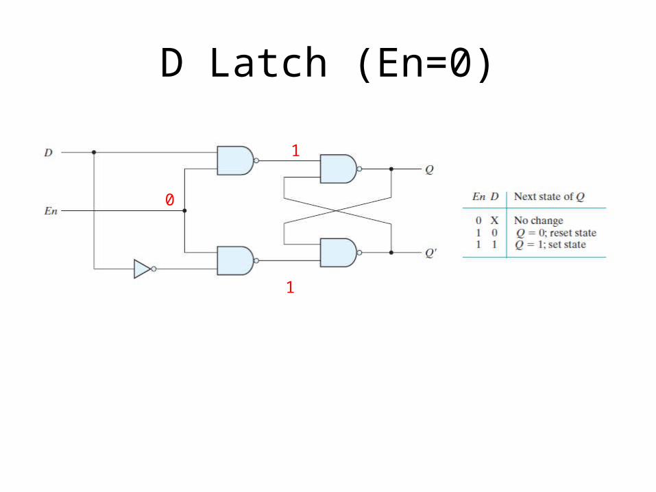
D Latch (En=0)
0
1
1
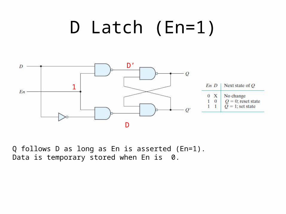
D Latch (En=1)
1
D’
D
Q follows D as long as En is asserted (En=1).Data is temporary stored when En is 0.

D-latch Operation
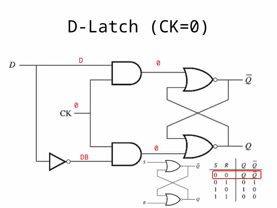
D-Latch (CK=0)
0
D
DB
0
0
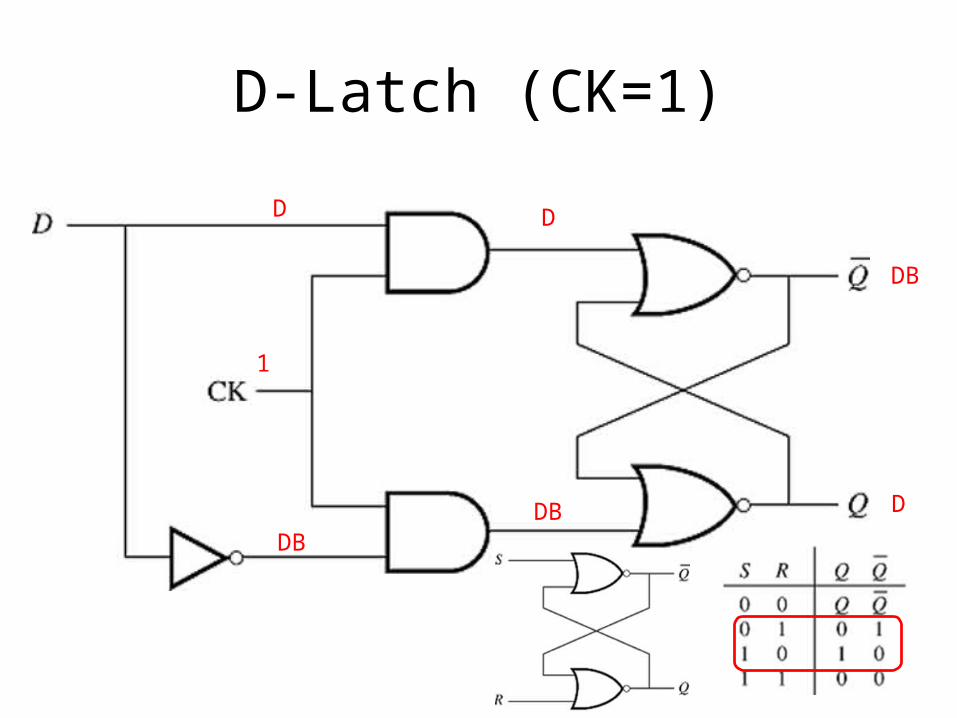
D-Latch (CK=1)
1
D
DB
D
DB D
DB
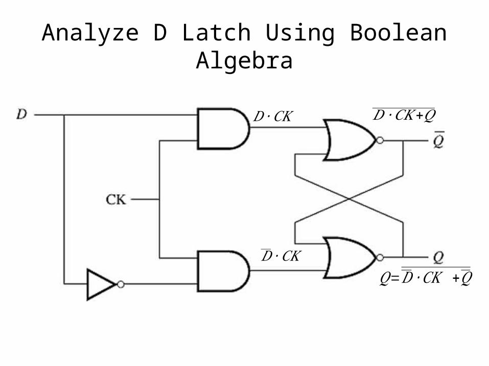
Analyze D Latch Using Boolean Algebra
𝐷 ∙𝐶𝐾
𝐷 ∙𝐶𝐾
𝐷 ∙𝐶𝐾 +𝑄
𝑄=𝐷 ∙𝐶𝐾 +𝑄
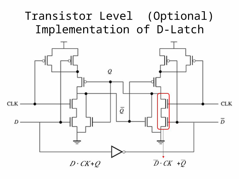
Transistor Level (Optional)Implementation of D-Latch
𝐷 ∙𝐶𝐾 +𝑄𝐷 ∙𝐶𝐾 +𝑄
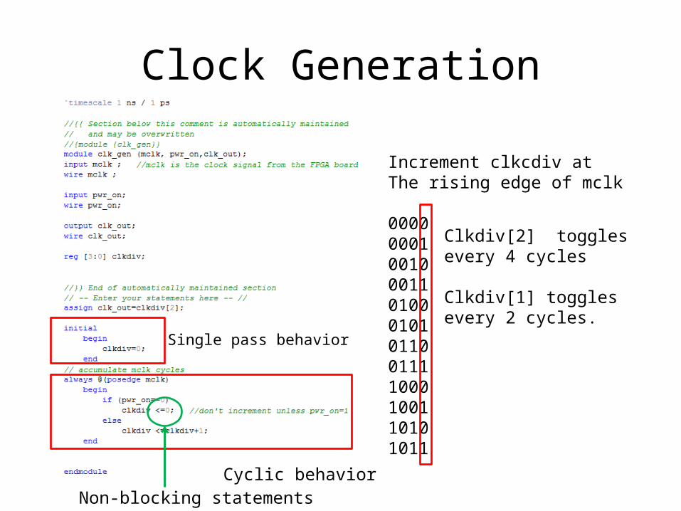
Clock Generation
Increment clkcdiv atThe rising edge of mclk
000000010010001101000101011001111000100110101011
Clkdiv[2] toggles every 4 cycles
Clkdiv[1] toggles every 2 cycles.
Single pass behavior
Cyclic behaviorNon-blocking statements
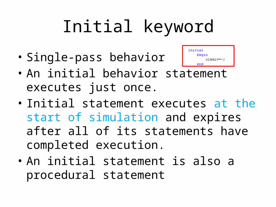
Initial keyword
• Single-pass behavior• An initial behavior statement executes
just once.• Initial statement executes at the start
of simulation and expires after all of its statements have completed execution.
• An initial statement is also a procedural statement
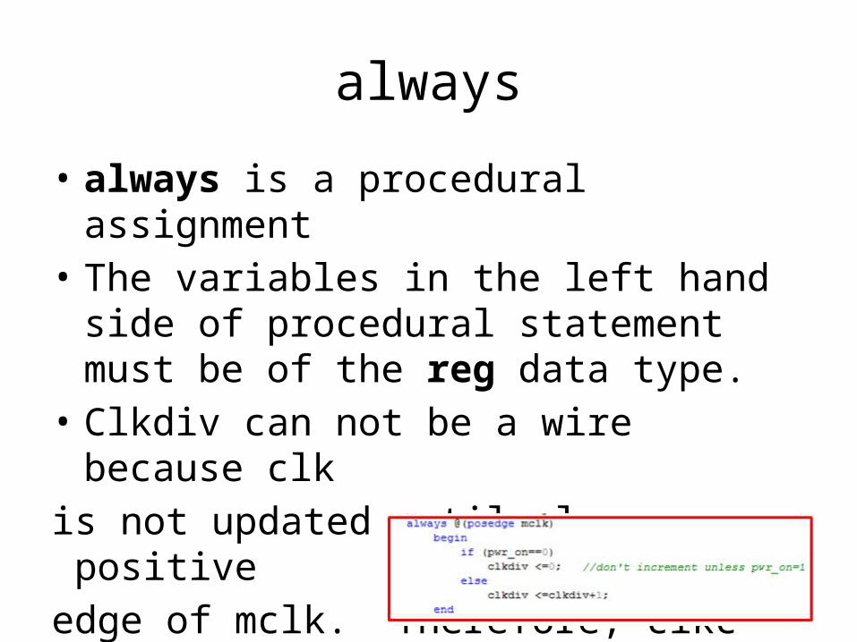
always
• always is a procedural assignment• The variables in the left hand side of
procedural statement must be of the reg data type.
• Clkdiv can not be a wire because clkis not updated until always sees positiveedge of mclk. Therefore, clkc can not be a wire type.
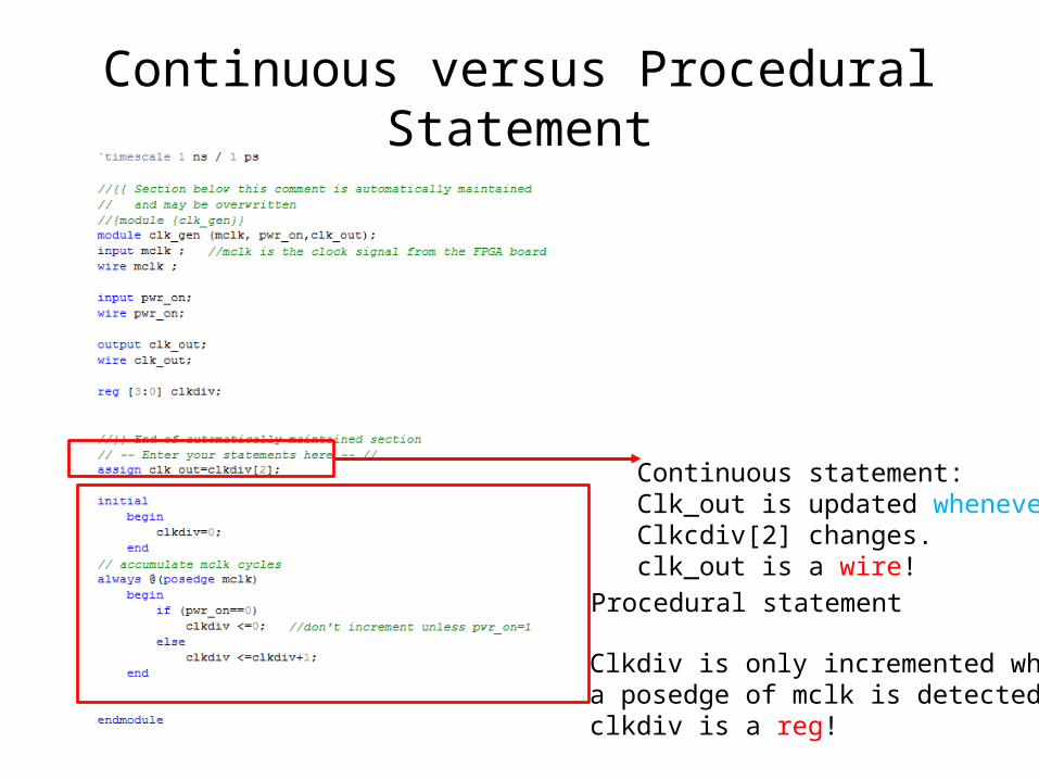
Continuous versus Procedural Statement
Procedural statement
Continuous statement:Clk_out is updated wheneverClkcdiv[2] changes.clk_out is a wire!
Clkdiv is only incremented whena posedge of mclk is detected.clkdiv is a reg!

Blocking versus Nonblocking Statements
• There are two kinds of procedural assignments:– Blocking statements
• Use (=) as the assignment operator• Blocking statements are executed sequentially in
the order they are listed.• Used to model behavior that are level sensitive (i.e.
in combinational logic)
– Nonblocking statements• Use (<=) as the assignment operator• Nonblocking statements are executed concurrently.• Used to model synchronous/concurrent behavior.
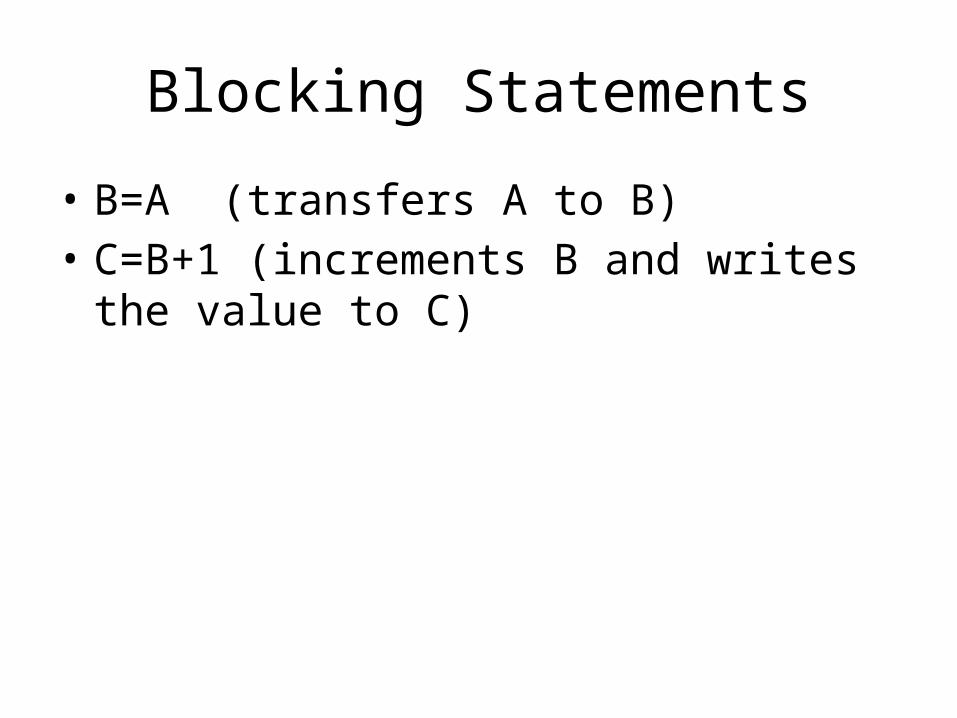
Blocking Statements
• B=A (transfers A to B)• C=B+1 (increments B and writes the
value to C)
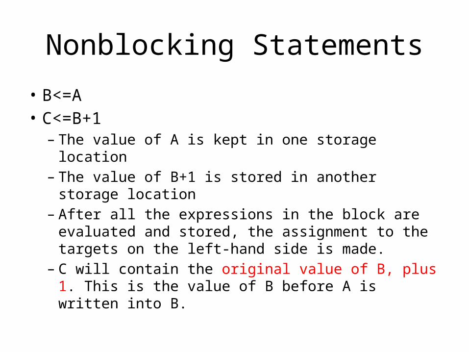
Nonblocking Statements
• B<=A• C<=B+1– The value of A is kept in one storage location – The value of B+1 is stored in another storage
location– After all the expressions in the block are
evaluated and stored, the assignment to the targets on the left-hand side is made.
– C will contain the original value of B, plus 1. This is the value of B before A is written into B.
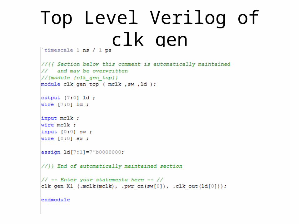
Top Level Verilog of clk_gen

Generate a Test Vector
Load test vector at t=0
Set dout equal to testvector[vectornum]at the rising edge of a dclk
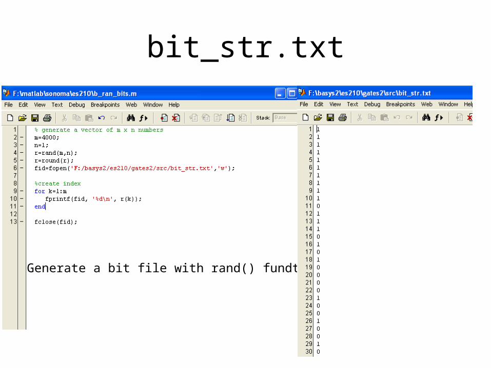
bit_str.txt
Generate a bit file with rand() fundtion
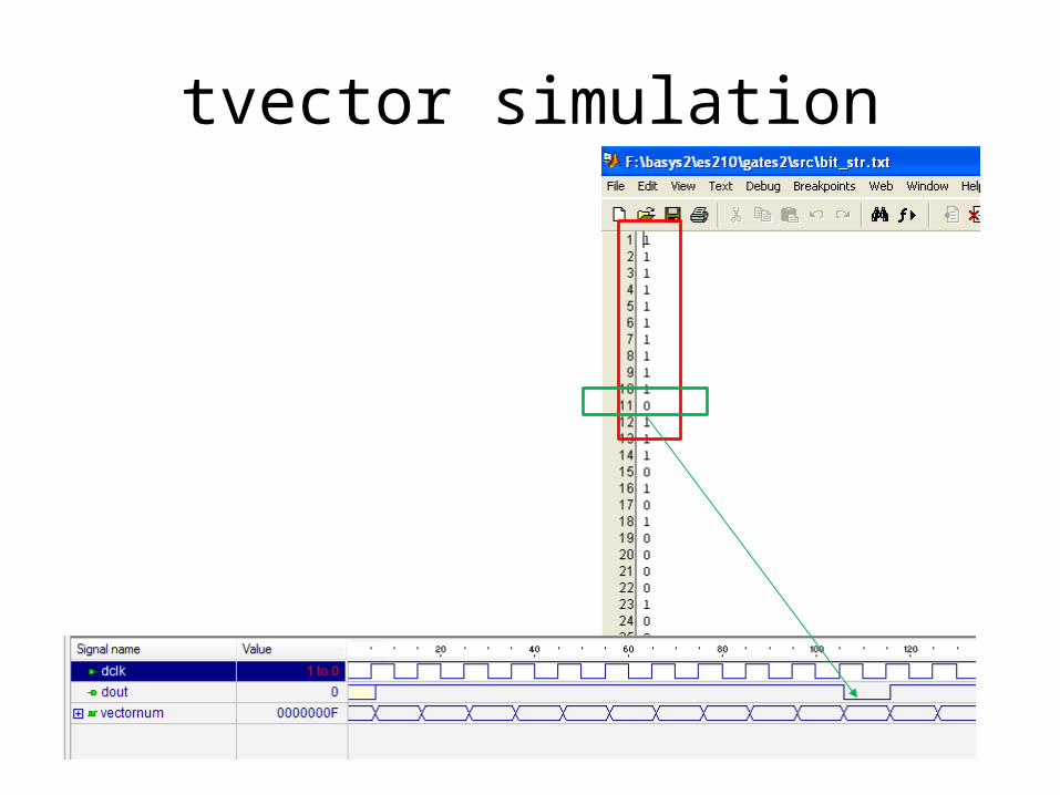
tvector simulation
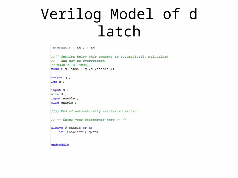
Verilog Model of d latch
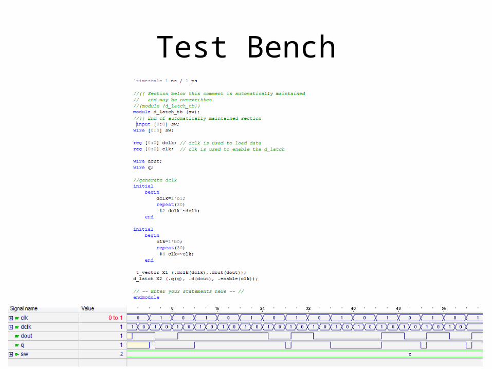
Test Bench
Use a Digital Oscilloscope
• Generate a binary vector in matlab• Load the binary vector onto the
function generator