lab-report analogue electronics - medizinlektorat dr ... · pdf filelab-report analogue...
TRANSCRIPT

Lab-ReportAnalogue Electronics
The Common-Emitter Amplifier
Name: Dirk BeckerCourse: BEng 2Group: AStudent No.: 9801351Date: 30/10/1998

2
1. Contents
1. CONTENTS............................................................................................................................................22. INTRODUCTION .................................................................................................................................. 33. DC BIAS OF COMM ON-EMITTER AMPLIFIER ...........................................................................3
a) Measurment of the “ true” resistor values.................................................................................................. 3b) DC-bias precalculation with given resistors.............................................................................................4c) Measurement of DC-Voltages (DC-bias) ................................................................................................. 5d) Calculation of IB, IC and β with measured values.....................................................................................5
i. IB with IE and IC (RE and RC)................................................................ ................................ ..................... 5ii. IB with I1 and I2 (R1 and R2) ................................................................ ................................ ................. 5
4. AC AND SMALL SIGNAL CHARACTERISTICS............................................................................6a) BJT small signal behavioural model .........................................................................................................6b) Definitions of the small signal parameters................................................................................................6c) Measured small signal values...................................................................................................................7d) Calculation and derivation of the small signal parameters .......................................................................7
i. Amplifier input resistance Ri................................................................ ................................ ..................... 7ii. Amplifier output resistance Ro ................................................................ ................................ ............. 8iii. Voltage amplification without load Avo ................................................................ ................................ 9iv. Voltage amplification with load Av ................................................................ ................................ ...... 9v. Current amplification Ai ................................................................ ................................ .................... 10vi. Amplifier power gain Ap................................................................ ................................ ..................... 10
e) Comparison between measured and calculated values...........................................................................11i. DC-Bias ................................................................ ................................ ................................ .................. 11ii. Small signal parameters................................................................ ................................ ..................... 11
5. FREQUENCY RESPONSE OF THE CE-AMPLIFIER................................................................... 12a) Measured frequency response of Av .......................................................................................................12b) Determination of the theoretical cut-off f requency.................................................................................13c) Frequency response of A i........................................................................................................................16
6. DISCONNECTION OF BYPASS CAPACITOR C3 .........................................................................187. DC-BIAS WITH DISCONNECTED C3 .............................................................................................18
a) Calculation of DC-Bias...........................................................................................................................18b) Measurement of DC-Voltages (DC-bias) ...............................................................................................18c) Calculation of IB, IC and β with measured values( C3 disconnected)......................................................19
i. IB with IE and IC (RE and RC)................................................................ ................................ ................... 19ii. IB with I1 and I2 (R1 and R2) ................................................................ ................................ ............... 19
8. AC AND SMALL SIGNAL CHARACTERISTICS (WITHOUT C3) .............................................20a) BJT small signal behavioural model .......................................................................................................20b) Measured small signal values without C3 ...............................................................................................20c) Calculation and derivation of the small signal parameters (mid freq., without C3) ................................21
i. Amplifier input resistance Ri................................................................ ................................ ................... 21ii. Amplifier output resistance Ro ................................................................ ................................ ........... 22iii. Voltage amplification at mid frequencies without load................................................................ ...... 22iv. Voltage amplification at mid frequencies with load................................................................ ........... 23v. Current amplification Ai ................................................................ ................................ .................... 23vi. Amplifier power gain Ap................................................................ ................................ ..................... 24
d) Comparison between measured and calculated values...........................................................................249. FREQUENCY RESPONSE OF THE CE-AMPLIFIER WITHOUT C3.........................................25
a) Frequency response of Av .......................................................................................................................25b) Theoretical calculation of the lower cut-off frequency...........................................................................27c) Frequency response of A i without C3......................................................................................................29

3
2. Introduction
The common-emitter ampli fier is one of the most common discrete ampli fier used inconventional electronics. Its special characteristics were to be discovered in this lab session.
3. DC bias of common-emitter ampli fier
figure 1
a) Measurment of the “ true” resistor values
For calculating the correct bias values at first the real values of the used resistors andcapacitors have to be measured, because they all have got deviations from the printed values.
Also a measurement of the very small currents is not possible. So the voltage drop across thedifferent devices has to be determined and then the flowing current can be calculated via KCLand Ohm’s law.
The following values were measured:
RS=3.26kΩ C1=80.54µFR1=9.99kΩ C2=8.949µFR2=55.7kΩ C3=9.177µFRE=986ΩRC=3.82kΩRL=6.72kΩ
4
( )( )
V907.2V
V454.1V639.5V10V
VVVV
V454.1V
201A232.71000V
1I[RIRV
V639.5V
mA446.1k9.3V
IRV
mA446.1A232.7200II
A232.7k485.810001000200
V10k56k10
k10
RR
RRRR
VRR
R
RRR
VI
CE
CE
RERECCCE
RE
RE
BCEERE
RC
RC
CCRC
BC
21
21EE
CC21
1
IEE
OB
=−−=
−−=
=⋅µΩ=+β==
=⋅Ω=
=
=µ⋅=β=
µ=Ω+Ω+Ω⋅
Ω+ΩΩ
=
+++β
+=
++β=
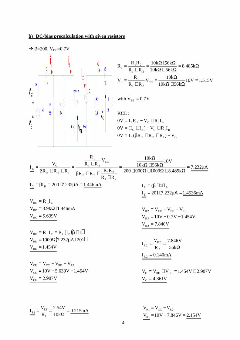
b) DC-bias precalculation with given resistors β=200, VBE=0.7V
O1EEB
BIOBC
BIOEE
BE
CC21
1o
21
21I
V)RRR(IV0
IRV)II(V0
IRVRIV0
:KCL
V7.0Vwith
V515.1V10k56k10
k10V
RR
RV
k485.8k56k10
k56k10
RR
RRR
−++β=+−+=
+−=
=
=Ω+Ω
Ω=+
=
Ω=Ω+ΩΩ⋅Ω=
+=
! "
! "
#$ % & ' ( ) * + ( ,- .
- / 0 , - ! , 0 1 2 ,- 3
#$ 4 -
5 1 6 ,- 7 + 8 - 7 9 " :
V361.4V
V907.2V454.1VVV
mA140.0I
k56
V846.7
R
VI
V846.7V
V454.1V7.0V10V
VVVV
mA4536.1232.7201I
(I
C
CEREC
2R
2
2R2R
2R
2R
REBECC2R
E
E
=+=+=
=Ω
==
=−−=
−−=
=Αµ⋅=Ι1)+β= Β
mA215.0k10
V54.2
R
VI
1
1R1R =
Ω==
V154.2V846.7V10V
VVV
1R
2RCC1R
=−=−=

5
c) Measurement of DC-Voltages (DC-bias)
Next step was to measure the voltages in order to check the real bias and to calculate based onthis values the DC current ampli fication and the other occurring currents and voltages.
VR1=1.477V
VR2=8.51VVRE=0.863VVRC=3.33VVC=6.66VBE=0.618VCE=5.80
d) Calculation of IB, IC and ββ with measured values
i. IB with IE and IC (RE and RC)
ii . IB with I 1 and I2 (R1 and R2)
177A93.4
mA8713.0
I
I
93.4mA14785.0mA15278.0III
mA15278.0k7.55
V51.8
R
VI
mA14785.0k99.9
V477.1
R
VI
B
C
1R2RB
2
2R2R
1
1R1R
=µ
==β
Αµ=−=−=
=Ω
==
=Ω
==
235A7.3
mA8713.0
I
Ih
A7.3I
mA8713.0mA875.0I
III
mA8713.0k82.3
V33.3
R
VI
mA875.0986
V863.0
R
VI
B
Cfe
B
B
CEB
C
RCC
E
REE
=µ
===β
µ=−=
−=
=Ω
==
=Ω
==

6
4. AC and small signal characteristics
Next part of the lab was to determine the small signal characteristics of the common-emitterampli fier. Small signal characteristics are the essential values for the ampli fication function ofthe circuit.
For calculation of these characteristics a special model is used, the small signal model of theBJT. These models are derived from the characteristic curves of the real devices and, whenproperly devised, can be used to predict accurately the behaviour of semiconductor devices inpractical applications such as voltage and current ampli fication.
By computer simulation more complex models can be used.
a) BJT small signal behavioural model
; <; = <
; > ; ?
@ A @ ?@ B@ C
DE F GH I J
KJ L
H G M NL H O
G PL Q R S T U V S U W S X R H Y H Z
N K [L
figure 2
In the small signal model for mid frequencies the capacitors are short circuited because theirimpedance is negligble to the rest of the circuit.
b) Definitions of the small signal parameters
voc: open circuit output voltagevo: output voltage with loadvs: signal voltagevi: ampifier input voltagevrs: voltage drop across sensor resistorRi: ampli fier input resistanceRo: ampli fier output resistanceAvo: ampli fier voltage gain without loadAv: ampli fier voltage gain with loadA i: ampli fier current gainAp: ampli fier power gain

7
c) Measured small signal values(A generator with f=1kHz works as voltage source V1)
vs=20mVvoc=1.242Vvo=0.799Vvi=10.8mVvrs=9.1mV
d) Calculation and derivation of the small signal parameters
ALL THEORETICAL VALUES WITH INDEX ‘ (i.e. R’)
i. Ampli fier input resistance Ri
The theoretical value of Ri fits good with the determination due the measured values. Themeasurement of vi and i i was relative uncertain because of the small values and not using thewhole range of the measuring instrument (~20mV to 200mV Range).
\ ]\ ^ ]
\ _
` a` b
cd e fg h i
ji k
g l m n k g f f ok p q r s t u r
Ω=Ω
=== k87.3
k26.3mV1.9
mV8.10
rvv
i
vR
:R of valueMeasured
s
rs
i
i
ii
i
Ω=
Ω+
Ω+
Ω
=
ΩΩ=
=
==
==
k52.2
k578.31
k561
k101
1'R
mA453.1
mV26200||k56||k10'R
I
mV26h||R||R'R
I
mV26r with rh||R||R'R
h||R||Ri
v'R
:Rfor Values lTheoretica
i
i
Efe21i
Eeefe21i
ie21i
ii
i
figure 3

8
ii . Ampli fier output resistance Ro
v w x v w
y x
z | ~
|
figure 4
From these in the lab measured values hOE can be easily determined:
Ω=Ω
−Ω
=−
=
−=
+=
k1.142h
k82.3
1
k72.3
11
R
1
R
11
h
R
1
R
1
h
1
R
1
h
1
R
1
OE
CO
OE
COOE
COEO
It can be seen, that hOE can be let out at calculation of BJTs, because of its large value to therest of the circuit.
Ω=Ω
−=
−=
k72.3
k72.6V799.0
V799.0V242.1R
Rv
vvR
:R of valueMeasured
o
L
o
ooco
o
Ω===
k9.3'R
S0h withR'R
:R of valuelTheoretica
o
OECo
o

9
iii . Voltage ampli fication without load Avo
iv. Voltage ampli fication with load Av
218
mA4536.1mV26
k9.3'A
I
mV26h
Rh
h
Rh'A
ih
Rih
ih
Ri'A
v
v'A
:A of valueslTheoretica
vo
Efe
Cfe
ie
Cfevo
Bie
CBfe
Bie
Ccvo
Ri
ocvo
vo
L
=Ω=
−=−=
−=−
=
= ∞→
( )
( ) ( )
138
mA4536.1mV26
k479.2'A
ImV26
RR
RR
ImV26
RR'A
I
mV26h
RRh
h
RRh'A
ih
RRi'A
v
v'A
:A of valuelTheoretica
v
E
LC
LC
E
LCv
Efe
Lcfe
ie
Lcfev
Bie
LCcv
i
ov
v
=Ω=
+⋅
==
=−=
−=
=
115AmV8.10
V242.1A
v
vA
:A of valueMeasured
vo
vo
i
ocvo
vo
=
=
=
74AmV8.10
V799.0A
v
vA
:A of valueMeasured
v
v
i
ov
v
=
=
=

10
v. Current ampli fication A i
vi. Ampli fier power gain Ap
140'Ak485.8k58.3
k485.8200'A
RRImV26h
RRh
RRh
RRh'A
iRRh
RRiwith
i
ih'A
i
i'A
:A of valuelTheoretica
i
i
21E
fe
21fe
21ie
21fei
I21ie
21B
I
Bfei
I
Ci
i
=Ω+Ω
Ω=
+=
+=
+==
=
117Ak26.3
mV1.9k82.3
V242.1A
Rv
Rv
i
iA
:A of valueMeasured
i
i
s
rs
c
oc
I
Ci
i
=Ω
Ω=
==
( )
19494'AmA1436.1
mV26k479.2
k458.8k58.3
k458.8200'A
ImV26
RR
Rh
Rh'A
h
RRh
Rh
Rh'A
AA'A
:A of valuesTheeoretic
p
p
E
LC
Iie
Ifep
ie
LCfe
Iie
Ifep
vip
p
=
Ω⋅Ω+Ω
Ω=
+=
+=
⋅=
8658'A
11774'A
AA'A
:A of valueMeasured
p
p
vip
p
=
⋅=
⋅=

11
e) Compar ison between measured and calculated values
i. DC-Bias
Measurand VRC VRE VCE VC VR1 VR2 hfe
measured 3.33V 0.863V 5.80V 6.66V 2.154V 7.846V 237/177
calculated 5.639V 1.454V 2.907V 4.361V 2.154V 7.846V 200
ii . Small signal parameters
Measurand Rin Rout Avo Av A i Ap
measured 3.87 kΩ 3.72kΩ 115 74 117 8685calculated 2.52 kΩ 3.9kΩ 218 138 140 19494
The measured and the calculated values are partly very different. Major problem of thedetermination of the Bias and the small signal parameters were the uncertain measurements.Especially the small values like IB and the input current of the small signal equivalent circuitwere very diff icult to determine exactly.

12
5. Frequency response of the CE-amplifier
a) Measured frequency response of Av
The voltage ampli fication over a range from 10Hz to 1kHz was to measure to determine thecut-off frequency of the CE-Ampli fier.
f/Hz 10 20 50 70 100 120 200 500 700 1000vi/mV 13.1 12.8 11.4 11.1 10.7 11.4 10.2 10 10 10vo/mV 183.4 0.324 555 618 667 730 714 734 736 738vo/vi 14 25.31 48.7 55.7 62.3 64 70 73.4 73.6 73.8
The cut-off frequency is defined as the frequency, when the ampli fication is dropped down to70.7% (-3dB or ½√2).Below this frequency there is still ampli fication, but the frequency range of ampli fiers iscommonly defined by the 3dB cut-off freuency.
Voltage Amplification vs frequency
10
100
10 100 1000f
Av
maxvA2
1dB3 =−
figure 5
fc=58Hz

13
b) Determination of the theoretical cut-off f requency
¡ ¢ £ ¤ ¥ ¥
figure 6
Figure 6 shows the equivalent circuit for low and mid frequencies.To determine the cut-off frequency the input and output circuit has to be separated.
figure 7
¦ §¦ ¨ ¦ ©¦ ª
« ¬ « ®« ¬ ®
« ©¯ °± ² ³¯ ±± ² ³
´ ¯µ ¶ · ¸ ¹ º ·± »¼ ½
¼ °¾ ¿ » ¼ ±± ² » ¿ À Á »¼  à ± ¼ ¯Ä À Å »Æ Ç È É Æ Ç Ê Ë Ì« ¨
The cut-off frequency of the CE-Ampli fier is above all depending on the emitter bypasscapacitor CE=C3. The impedance of the two coupling capacitors is about 1500Ω at 10Hz eachand can be neglected because of these small values in comparison to the rest of the circuit.
For the input circuit:
1
Cj
R)1(
1Cj
R
11
1)Z( Zwhere
ZRh
vI
E
E
EE
EEIn
EInInie
iB
+βω+
+β
1=ω+
+β=+β=
++=
Input OutputCurrent sourceÍ ic=constant

14
The current through (β+1)RE can be neglected because of it’s large resistance
EInie
inB
C
1jRh
vi
ω+β−+
=
The current IB will drop to 70.7% of it’s maximum value when the voltage drop at (hie+RIn)and ZE are of the same magnitude.
Hz54f2
f
s
1337
)k577.3k38.2(F100
201
k38.2RRRR where)hR(C
1
hR
1
C1
cc
c
S21inieinE
cutoff
ieInE
=π
ω=
=Ω+Ωµ
=ω
Ω==+
+β=ω
+=
+βω
The calculated cut-off f requency is with 54Hz very close at the measured value of 58 Hz.The exact calculation of the cut-off frequency is very complex and is done in most cases witha computer and a simulation software like (P) or (H)spice.On the following pages (P)spice printouts of the simulated CE-Ampli fier can be found.
Î Ï Ï ÐÑ Ò
Î Ï ÐÑ Î Î Ï ÐÑ Ó
Ò Ô Õ Ö× Ñ
Ø Ó Ù Ó Ó Ó ÓØ Î
Î Ö× Ú× Î Î Ï ÖÒ Ô Ò Ö× ÛÜÝ Þ Û
ß à Ö× Ó
× á à Ô â ÖÜÝÎ Ó Þ Þ ÎÎ Ô ã à Ï Þ
ã Ô à â à ÞÎ Ô Î Î Ò Þ
Î Ô Î Ï à ä å
à Ô Õ Î æ Ð å
Î Ô Î Î Ò ä å
Î â Ó Ô â ã Ð å
figure 8
figure 8 shows the BIAS calculated by a (P)spice simulation.

15
Spice printout of frequency response AV
16
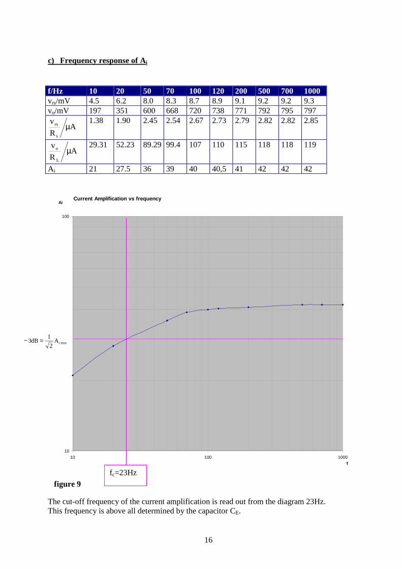
c) Frequency response of A i
f/Hz 10 20 50 70 100 120 200 500 700 1000vrs/mV 4.5 6.2 8.0 8.3 8.7 8.9 9.1 9.2 9.2 9.3vo/mV 197 351 600 668 720 738 771 792 795 797
AR
v
s
rs µ1.38 1.90 2.45 2.54 2.67 2.73 2.79 2.82 2.82 2.85
AR
v
L
o µ29.31 52.23 89.29 99.4 107 110 115 118 118 119
A i 21 27.5 36 39 40 40,5 41 42 42 42
The cut-off frequency of the current ampli fication is read out from the diagram 23Hz.This frequency is above all determined by the capacitor CE.
Current Amplification vs frequency
10
100
10 100 1000f
Ai
maxiA2
1dB3 =−
fc=23Hz
figure 9

17
Spice printout of the frequency response of the current ampli fication A i vs frequency

18
6. Disconnection of bypass capacitor C3
Next step of the Lab was to disconnect the Emitter bypass capacitor to proof the importanceof the bypass capacitor especially on the voltage and current ampli fication, the main
çè é
ç
ê é ë ìì éí î í í í íé ë ï é ë ïè íð ñ ð òó ô
õ ö òó í ð ñ ÷ òó è
é òó øó éé ë ò ó ùö ñ ú òê ì ôfigure 10
Figure 10 shows the schematics of the CE-Ampli fier with disconnected C3.
7. DC-Bias with disconnected C3
a) Calculation of DC-Bias
The calculated DC-Bias with disconnected capacitor C3 can’ t change, because C3 has noinfluence to any DC-values. C3 is not used for calculation of the DC-Bias and so it’s not ableto change it.û
see DC-Bias values at DC-bias precalculation with given resistors
b) Measurement of DC-Voltages (DC-bias)
The same DC-bias measurements were to make with disconnected C3 li ke in the first part ofthe Lab.
VR1=1.479V
VR2=8.47VVRE=0.849VVRC=3.27VVC=6.65VBE=0.625VCE=5.81

19
c) Calculation of IB, IC and ββ with measured values( C3 disconnected)
i. IB with IE and IC (RE and RC)
ii . IB with I 1 and I2 (R1 and R2)
213A01.4
mA856.0
I
I
01.4mA14805.0mA15206.0III
mA15206.0k7.55
V47.8
R
VI
mA14805.0k99.9
V479.1
R
VI
B
C
1R2RB
2
2R2R
1
1R1R
=µ
==β
Αµ=−=−=
=Ω
==
=Ω
==
The different values of β=hfe can be led back to the uncertainty of measurement, because themeasured values were very small and at the lower range of the measuring instrument.
2.171A5
mA856.0
I
Ih
A5I
mA856.0mA861.0I
III
mA856.0k82.3
V27.3
R
VI
mA861.0986
V849.0
R
VI
B
Cfe
B
B
CEB
C
RCC
E
REE
=µ
===β
µ=−=
−=
=Ω
==
=Ω
==

20
8. AC and small signal characteristics (without C3)
Next part of the lab was to determine the small signal characteristics of the common-emitterampli fier.
By computer simulation more complex models can be used.
a) BJT small signal behavioural model
With the disconnected Capacitor C3 another model of the circuit has to be used now, becausethe Emitter Resistor is now not short circuited at mid-frequencies and generates an importantcurrent feedback of the AC-signals through IE, which reduces the ampli fication of the CE-Ampli fier considerably.
ü ýü þ ü ÿü
ü
ÿ
figure 11
All the definitions can be taken from Definitions of the small signal parameters
b) Measured small signal values without C3
The input voltages are increased by a factor 10 to obtain better measurands at the low
ampli fications without bypass capacitor.(A generator with f=1kHz works as voltage source V1)
vs=200mVvoc=533mVvo=340mVvi=143mVvrs=57.3mV

21
c) Calculation and derivation of the small signal parameters (mid freq., without C3)
ALL THEORETICAL VALUES WITH INDEX ‘ (i.e. R’)
i. Ampli fier input resistance Ri
TheFigure 12 shows, that the Emitter resistor is divided into two parts for separating input andoutput circuit.The connection between both is given through the voltage drop at the emitter resistor RE.
The calculated value of Rin is very close to the measured value. The approximation of REin canbe done because there’s a negligible difference between hfe and (hfe+1).
[ ]
Ω≈Ω×+Ω
+Ω
+Ω
≈
+≈
++=
+==+=
k15.8'Rk1200k577.3
1
k10
1
k56
11
'R
)Rhh(RR'R
R)1h(hRR'R
i
iR)1h(
i
vR where)Rh(RR'R
:R of valuelTheoretica
in
in
Efeie12in
Efeie12in
B
BEfe
B
REEInEInie12in
in
! " # $
% & '% (% & (
% #
) *+ , -) ++ , - ./ 0 )1 2 3 4 5 6 3+ 78 9
8 *: ; 7 8 ++ , 7 ; < = 78 >./ ? + 8 )@ < A 78 B 6 C 8 B D - E
Ω=Ω
=
==
k14.8Rk26.3
mV3.57mV143
R
Rv
v
i
vR
:R of Value Measured
in
in
s
rs
i
i
iin
in
figure 12

22
ii . Ampli fier output resistance Ro
F G H F G
I H
JK L MN O P Q
L R
figure 13
It’s the same small signal model than in the first part. The series connection of the currentsource and the emitter resistor can be reduced to the current source only.
The calculated and the measured value are again very close together.
iii . Voltage ampli fication at mid frequencies without load
83.3k1200k577.3
k9.3200A
Rhh
Rh
R)1h(h
RhA
)Rh(
RhA
)Rh(i
Rih
v
v'A
:A of valuelTheoretica
vo
Efeie
Cfe
Efeie
Cfevo
Einie
Cfevo
EinieB
CBfe
i
ocvo
vo
=Ω⋅+Ω
Ω⋅=
+≈
++−=
+−
=
+−
==
The Voltage ampli fication is very low, because the emitter resistor without bypass capacitorcauses a current feedback which results in a low Ampli fication at all frequencies (seefrequency response).
Ω=Ω
−=
−=
k81.3
k72.6mV340
mV340mV533R
Rv
vvR
:R of valueMeasured
o
L
o
ooco
o
Ω===
k9.3'R
S0h withR'R
:R of valuelTheoretica
o
OECo
o
3.3amV143
mV533A
v
vA
:A of valueMeasured
vo
vo
i
ocvo
vo
=
=
=

23
iv. Voltage ampli fication at mid frequencies with load
45.2k1200k577.3k8.6k9.3
k8.6k9.3200
'A
Rhh
)RR(h
R)1h(h
)RR(h'A
)Rh(
)RR(h'A
)Rh(i
)RR(ih
v
v'A
:A of valuelTheoretica
v
Efeie
LCfe
Efeie
LCfev
Einie
LCfev
EinieB
LCBfe
i
ov
vo
=Ω⋅+ΩΩ+ΩΩ⋅Ω⋅
=
+≈
++−=
+−
=
+−
==
The ampli fication without bypass capacitor is again very low, but the theoretical value and themeasured value are very close together.
v. Current ampli fication A i
38.2AmV143
mV340A
v
vA
:A of valueMeasured
vo
vo
i
ocvo
vo
=
=
=
8'A
k485.8)201(k1k58.3
k485.8200'A
RR)1h(RImV26h
RRh
RR)1h(Rh
RRh'A
iRRR)1h(h
RRiwith
i
ih'A
i
i'A
:A of valuelTheoretica
i
i
21feEE
fe
21fe
21feEie
21fei
I21Efeie
21B
I
Bfei
I
Ci
i
≈Ω+Ω+Ω
Ω=
+++=
+++=
+++==
=
93.7Ak26.3
mV3.57k82.3
mV533A
Rv
Rv
i
iA
:A of valueMeasured
i
i
s
rs
c
oc
I
Ci
i
=Ω
Ω=
==

24
vi. Ampli fier power gain Ap
d) Compar ison between measured and calculated values
Measurand hfe Rin Rout Avo Av A i Ap
measured 171/213
8.14kΩ 3.81kΩ 3.3 2.38 8 19
calculated 200 8.15kΩ 3.9kΩ 3.83 2.45 8 19
19'A
k1200k577.3
k479.2
k48.8201k1k577.3
k48.8200'A
Rhh
RR
RR)1(Rh
RRh'A
AA'A
:A of valuesTheeoretic
p
p
Efe
ie
LC
21Eie
21fep
vip
p
=
Ω+ΩΩ×
Ω+⋅Ω+ΩΩ=
+×
++β+=
⋅=
19'A
38.293.7'A
AA'A
:A of valueMeasured
p
p
vip
p
=
⋅=
⋅=

25
9. Frequency response of the CE-amplifier without C3
a) Frequency response of Av
f/Hz 10 20 50 70 100 200 500 700 1000vi/mV 134 131.8 131.4 131.2 131.3 130.9 130.9 730.9 130.9vo/mV 305 309 311 310 311 310 310 310 310vo/vi 2.3 2.3 2.4 2.3 2.3 2.3 2.3 2.3 2.3
fc is notreadable
and so the cut-off frequency is much lower than 10Hz. The current ampli fication is linear overthe low and mid frequency band.
Voltage Amplification vs frequency
1
10
10 100 1000f
Av
figure 14

26
(P)spice printout of the Voltage Ampli fication without bypass capacitor

27
b) Theoretical calculation of the lower cut-off f requency
At this circuit only the coupling capacitors have an influence to the lower cut -off fr equencybecause the bypass capacitor is removed.
S TS U S VS W
X Y ZX [X Y [
X V
\ ]^ _ `\ ^^ _ ` ab c \d e f g h i f^ j
k lk ]m n j k ^^ _ j n o p jk qa
b r ^ k \s o t jk u ^ jX U
figure 15
figure 15 shows the small signal equivalent circuit for the CE-Ampfli fier with disconnectedbypass capacitor.
S TS U S VS W
X Y ZX [X Y [
X V
\ ]^ _ `\ ^^ _ ` ab c \d e f g h i f^ j
k lk ]m n j k ^^ _ j n o p jk qa
b r ^ k \s o t jv w x y v w z |X U
figure 16
In figure 16 the emitter resistor is separated into its input and output circuit part.
For the input circuit:
)Rh(RR wherev
CRj
11)Rh(
1i
Cj
1R
v
RhR
Ri
RhRR
RRi
Cj
1R
vi
EinieBini
1inEinie
B
1in
i
EinieB
Bi
Einie21
21B
in
ii
+=
ω
++=
ω+++
=++
=
ω+
=

28
For the output circuit:
B
2CL
feLCo
LC
LCLCb
2CL
feCLoLo
Bfe
2LC
Cc
2LC
Co
i
C)RR(j
11
h)RR(v
RR
RRRR wherei
Cj
1RR
hRRiRv
ih
Cj
1RR
Ri
Cj
1RR
Ri
+ω+
=
+=
ω++
−=−=
ω++
=
ω++
=
Combining the I /P and O/P circuit
[ ]
)s1)(s1(
sA
v
v)s(A
C)RR(
C)R)h1(h(RCR
R)h1(h
)RR(hA where
)Rh(CRj
11
1
C)RR(j
11
h)RR(
v
vA
21
221
vmidi
oV
2LC2
1EfeieB1In1
Efeie
LCfevmid
Einie1In2CL
feLC
i
ov
τ+τ+ττ
==
+=τ++==τ
++−=
+ω
++ω
+−==
Using the calculated values:
Hz2
55.1
)s(
s
A
)s(A
Hz48.12
fHz34.91
s107.0
F10)k8.6k9,3(
Hz95.12
f28.121
s081.0
F10)k14.8k48.8(
c
CL
2c
2
2
2c
2
mid21
21c
22
2
2
11c
11
1
1
≈ωω=ω
ω+ωω=
ω+=⇒ω≈ω
=π
ω=⇒=
τ=ω
=τµΩ+Ω=τ
=π
ω=⇒=τ
=ω
=τµΩΩ=τ
This low frequency was not measurable in the lab, because the generator and the measuringinstruments were not able to determine such a low frequency correctly.The ampli fication of the CE-Ampli fier without bypass capacitor reaches nearly into the DC-region.

29
figure 17
c) Frequency response of A i without C3
f/Hz 10 20 50 70 100 200 500 700 1000vrs/mV 56 57 57 57 57 57 57 57 57vo/mV 333 337 339 339 340 339 339 339 339
AR
v
s
rs µ17.17 17.5 17.5 17.5 17.5 17.5 17.5 17.5 17.5
AR
v
L
o µ49.55 50 50.5 50.5 50.5 50.5 50.5 50.5 50.5
A i 2.88 2.87 2.88 2.88 2.88 2.88 2.88 2.88 2.88
fc is not readable and so the cut-off frequency is much lower than 10Hz.
The current and voltage ampli fication of the CE-ampli fier is very low, but constant during thelower frequencies, therefor the CE-Ampli fier without bypass capacitor is not often used.For low frequency ampli fication usually direct coupled ampli fiers with bypass capacitors areused. If the circuit is well designed the lower cut-off frequency is mostly determined by theemitter capacitor and NOT by the coupling capacitors.
Current Amplification vs frequency
1
10
10 100 1000f
Ai

30
(P)spice printout of the current ampli fication vs frequency