kv4x data sheet - nxp semiconductorscache.freescale.com/files/32bit/doc/data_sheet/kv4xp100m...kv4x...
TRANSCRIPT

KV4x Data Sheet168 MHz ARM Cortex-M4 core based Microcontroller withFPU
The Kinetis KV4x MCU family is a member of the Kinetis Vseries and provides a high-performance solution for motorcontrol and Digital Power Conversion. Built upon the ARM®
Cortex®-M4 core operating at up to 168 MHz with DSP andfloating point unit, features include; dual 12-bit analog-to-digitalconverters with 240ns conversion time, up to 30 PWM channelsfor support of multi-motor systems, eFlexPWM module with 312ps resolution for digital power conversion applications,programmable delay block, memory protection unit, dualFlexCAN modules and 64 to 256 KB of flash memory. KV4xMCUs are offered in 48LQFP, 64LQFP, and 100LQFPpackages. All Kinetis V series MCUs are supported by acomprehensive enablement suite from NXP and third-partyresources including reference designs, software libraries andmotor configuration tools. KV4x MCUs are enabled to support Kinetis Motor Suite (KMS), a bundled hardwareand software solution that enables rapid configuration of BLDC and PMSM motor drive systems.
Core• ARM® Cortex®-M4 core up to 168 MHz with single
precision Floating Point Unit (FPU)
Memories• Up to 256 KB of program flash memory• Up to 32 KB of RAM
System peripherals• 16-channel DMA controller• Low-leakage wakeup unit• SWD interface and Micro Trace buffer• Advanced independent clocked watchdog
Clocks• 32 to 40 kHz or 3 to 32 MHz crystal oscillator• Multipurpose clock generator (MCG) with frequency-
locked loop and phase-locked loop referencing eitherinternal or external reference clock
Operating Characteristics
• Voltage range: 1.71 to 3.6 V• Temperature range: –40 to 105 °C
Human-machine interface• General-purpose input/output
Communication interfaces• Two Universal Asynchronous Receiver/Transmitter
(UART) / FlexSCI modules with programmable 8- or9-bit data format
• One 16-bit SPI module• One I2C module• Two FlexCAN modules
Analog Modules
• Two 12-bit cyclic ADCs• Four analog comparator (CMP) containing a 6-bit
DAC and programmable reference input• One 12-bit DAC
Timers• One eFlexPWM with 4 sub-modules, providing 12
PWM outputs• Two 8-channel FlexTimers (FTM0 and FTM3)• One 2-channel FlexTimers (FTM1)• Four Periodic interrupt timers (PIT)• Two Programmable Delay Blocks (PDB)• Quadrature Encoder/Decoder (ENC)• Ratio of timer input clock frequency vs. core
frequency is 1:2 when core frequency is 168 Mhz,and 1:1 when core frequency is less than or equal to100 Mhz
MKV46FxxxVLy16MKV44FxxxVLy16MKV42FxxxVLy16
100 LQFP14 x 14 x 1.4 Pitch 0.5
mm
64 LQFP10 x 10 x 1.4 Pitch 0.5
mm
48 LQFP7 x 7 x 1.4 Pitch 0.5 mm
NXP Semiconductors KV4XP100M168Data Sheet: Technical Data Rev. 3, 06/2016
NXP reserves the right to change the production detail specifications as may berequired to permit improvements in the design of its products.
Kinetis Motor Suite• Supports velocity and position control of BLDC and
PMSM motors• Implements Field Orient Control (FOC) using Back
EMF to improve motor efficiency• Utilizes SpinTAC control theory that improves overall
system performance and reliability
Security and integrity modules• Hardware CRC module to support fast cyclic
redundancy checks• External Watchdog Monitor (EWM)
NOTEThe 48-pin LQFP package for this product is not yet available. However, it is includedin a Package Your Way program for Kinetis MCUs. Visit nxp.com/KPYW for moredetails.
Orderable part numbers summary1
NXP partnumber
CPU
frequenc
y(MHz
)
Pincoun
t
Totalflash
memory
(KB)
SRAM
(KB)
ADC eFlexPWM PWM
Nano-
Edge
Flex Timers DAC
FlexCAN
ADCA
ADCB
PWMA
PWMB
PWMX
FTM0
FTM3
FTM1
CAN0
CAN1
MKV46F256VLL16
168 100 256 32 18ch 20ch 1x8ch 1x4ch Yes 1x8ch 1x8ch 1x2ch 1 1 1
MKV46F256VLH16
168 64 256 32 13ch 16ch 1x8ch — Yes 1x8ch 1x8ch 1x2ch 1 1 1
MKV46F128VLL16
168 100 128 24 18ch 20ch 1x8ch 1x4ch Yes 1x8ch 1x8ch 1x2ch 1 1 1
MKV46F128VLH16
168 64 128 24 13ch 16ch 1x8ch — Yes 1x8ch 1x8ch 1x2ch 1 1 1
MKV44F256VLL16
168 100 256 32 18ch 20ch 1x8ch 1x4ch Yes — — — 1 1 1
MKV44F256VLH16
168 64 256 32 13ch 16ch 1x8ch — Yes — — — 1 1 1
MKV44F128VLL16
168 100 128 24 18ch 20ch 1x8ch 1x4ch Yes — — — 1 1 1
MKV44F128VLH16
168 64 128 24 13ch 16ch 1x8ch — Yes — — — 1 1 1
MKV44F128VLF162
168 48 128 24 11ch 10ch 1x8ch — Yes — — — 1 1 —
MKV44F64VLH16
168 64 64 16 13ch 16ch 1x8ch — Yes — — — 1 1 1
MKV44F64VLF162
168 48 64 16 11ch 10ch 1x8ch — Yes — — — 1 1 —
MKV42F256VLL16
168 100 256 32 18ch 20ch — — — 1x8ch 1x8ch 1x2ch — 1 1
MKV42F256VLH16
168 64 256 32 13ch 16ch — — — 1x8ch 1x8ch 1x2ch — 1 1
MKV42F128VLL16
168 100 128 24 18ch 20ch — — — 1x8ch 1x8ch 1x2ch — 1 1
Table continues on the next page...
2 KV4x Data Sheet, Rev. 3, 06/2016
NXP Semiconductors
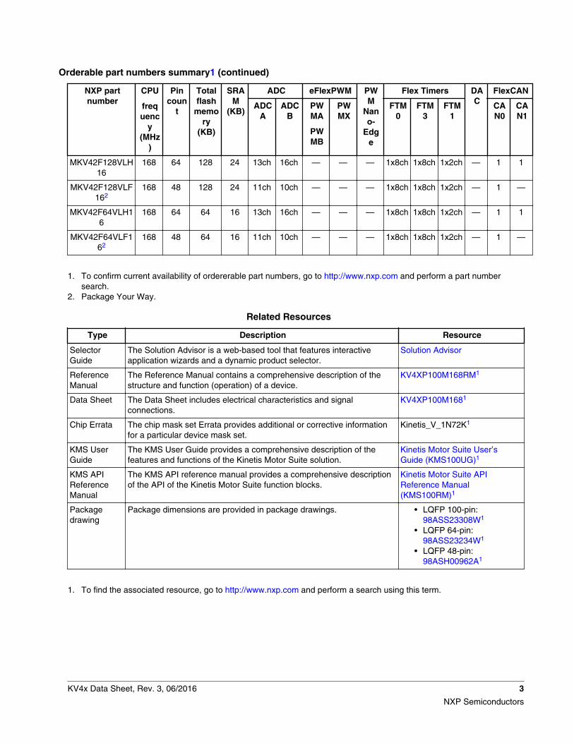
Orderable part numbers summary1 (continued)
NXP partnumber
CPU
frequenc
y(MHz
)
Pincoun
t
Totalflash
memory
(KB)
SRAM
(KB)
ADC eFlexPWM PWM
Nano-
Edge
Flex Timers DAC
FlexCAN
ADCA
ADCB
PWMA
PWMB
PWMX
FTM0
FTM3
FTM1
CAN0
CAN1
MKV42F128VLH16
168 64 128 24 13ch 16ch — — — 1x8ch 1x8ch 1x2ch — 1 1
MKV42F128VLF162
168 48 128 24 11ch 10ch — — — 1x8ch 1x8ch 1x2ch — 1 —
MKV42F64VLH16
168 64 64 16 13ch 16ch — — — 1x8ch 1x8ch 1x2ch — 1 1
MKV42F64VLF162
168 48 64 16 11ch 10ch — — — 1x8ch 1x8ch 1x2ch — 1 —
1. To confirm current availability of ordererable part numbers, go to http://www.nxp.com and perform a part numbersearch.
2. Package Your Way.
Related Resources
Type Description Resource
SelectorGuide
The Solution Advisor is a web-based tool that features interactiveapplication wizards and a dynamic product selector.
Solution Advisor
ReferenceManual
The Reference Manual contains a comprehensive description of thestructure and function (operation) of a device.
KV4XP100M168RM1
Data Sheet The Data Sheet includes electrical characteristics and signalconnections.
KV4XP100M1681
Chip Errata The chip mask set Errata provides additional or corrective informationfor a particular device mask set.
Kinetis_V_1N72K1
KMS UserGuide
The KMS User Guide provides a comprehensive description of thefeatures and functions of the Kinetis Motor Suite solution.
Kinetis Motor Suite User’sGuide (KMS100UG)1
KMS APIReferenceManual
The KMS API reference manual provides a comprehensive descriptionof the API of the Kinetis Motor Suite function blocks.
Kinetis Motor Suite APIReference Manual(KMS100RM)1
Packagedrawing
Package dimensions are provided in package drawings. • LQFP 100-pin:98ASS23308W1
• LQFP 64-pin:98ASS23234W1
• LQFP 48-pin:98ASH00962A1
1. To find the associated resource, go to http://www.nxp.com and perform a search using this term.
KV4x Data Sheet, Rev. 3, 06/2016 3
NXP Semiconductors
168 MHz
32-b it C P U
Crossbar switch (AXBS-Lite)
Peripheral bridge
FlexSCI SPI
WDOG1x 12 bitDAC
CRC
eFlexPWM
16 -chDMA
I2C SMBUS
GPIO
SRAMUp to 32 KB
P-FlashUp to 256 KB
4 - ch PIT
IRQ
12 bit ADC(4.1 MSPS)
32 kHzRC
MCG
OscLow range: 32 kHz
128
32
2 x PDB
EWM
FlexTimer8ch + 8ch +2ch
4 x HSCMPwith 6bit DAC
Up to 70
ARM Cortex M4
RCM SIM
MCM
PMC
JTAG/SWD
High range: 4-20 MHz
SPFPU
12 bit ADC
FlexCANFlexSCI
ENC XBARB
XBARA
AOI
nano-edge
x2
SPFPU
8 MHzRC
PLL 100-240 MHz
LPTMR
FMC
(4.1 MSPS)8ch + 4ch
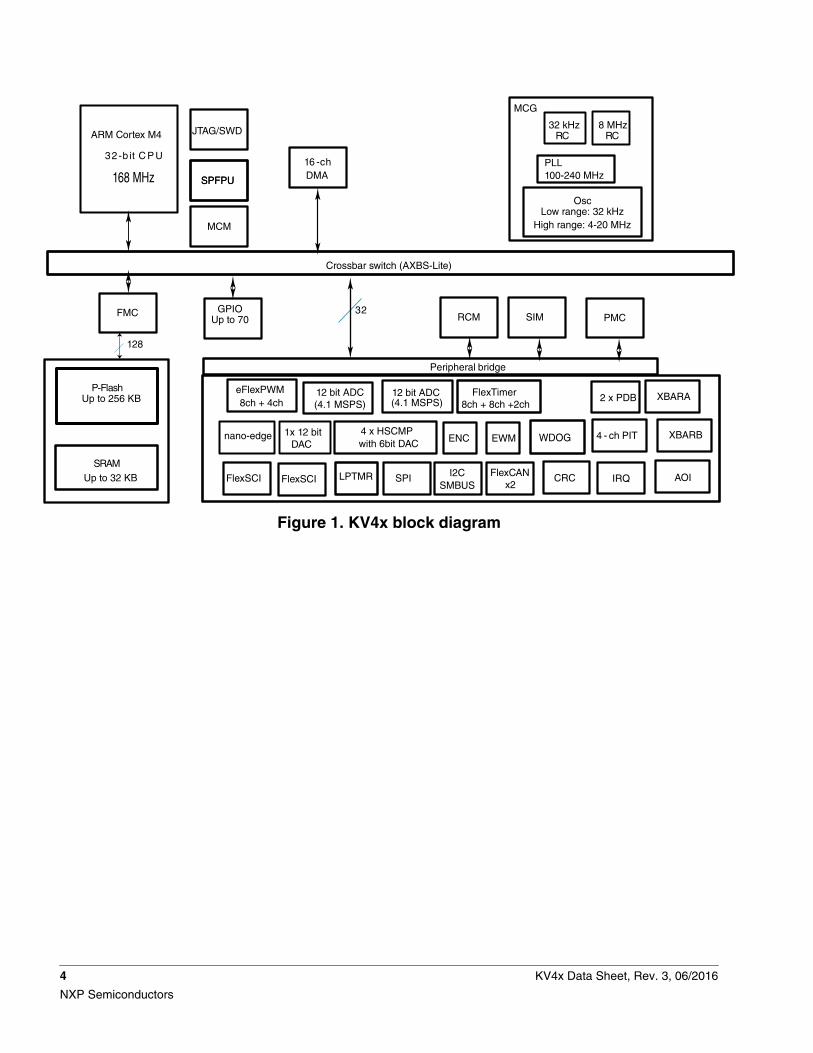
Figure 1. KV4x block diagram
4 KV4x Data Sheet, Rev. 3, 06/2016
NXP Semiconductors
Table of Contents
1 Ratings.................................................................................. 6
1.1 Thermal handling ratings............................................. 6
1.2 Moisture handling ratings.............................................6
1.3 ESD handling ratings................................................... 6
1.4 Voltage and current operating ratings..........................6
1.5 Absolute Maximum Ratings......................................... 7
2 General................................................................................. 8
2.1 AC electrical characteristics.........................................8
2.2 Nonswitching electrical specifications..........................9
2.2.1 Recommended Operating Conditions..............9
2.2.2 LVD and POR operating requirements............ 10
2.2.3 Voltage and current operating behaviors.........10
2.2.4 Power mode transition operating behaviors.... 11
2.2.5 Power consumption operating behaviors.........12
2.2.6 EMC radiated emissions operating behaviors. 17
2.2.7 Designing with radiated emissions in mind......18
2.2.8 Capacitance attributes..................................... 18
2.3 Switching specifications...............................................18
2.3.1 Typical device clock specifications.................. 18
2.3.2 General switching specifications......................19
2.4 Thermal specifications................................................. 20
2.4.1 Thermal operating requirements......................20
2.4.2 Thermal attributes............................................20
3 Peripheral operating requirements and behaviors................ 21
3.1 Core modules.............................................................. 21
3.1.1 SWD Electricals .............................................. 21
3.1.2 Debug trace timing specifications.................... 22
3.1.3 JTAG electricals...............................................23
3.2 System modules.......................................................... 26
3.3 Clock modules............................................................. 26
3.3.1 MCG specifications..........................................26
3.3.2 Oscillator electrical specifications.................... 28
3.4 Memories and memory interfaces............................... 30
3.4.1 Flash electrical specifications.......................... 30
3.5 Security and integrity modules.....................................31
3.6 Analog..........................................................................32
3.6.1 12-bit cyclic Analog-to-Digital Converter
(ADC) parameters............................................32
3.6.2 CMP and 6-bit DAC electrical specifications....34
3.6.3 12-bit DAC electrical characteristics................ 36
3.7 Timers..........................................................................39
3.8 Enhanced NanoEdge PWM characteristics.................39
3.9 Communication interfaces........................................... 40
3.9.1 SPI (DSPI) switching specifications (limited
voltage range)..................................................40
3.9.2 SPI (DSPI) switching specifications (full
voltage range)..................................................44
3.9.3 I2C................................................................... 47
3.9.4 UART............................................................... 47
3.10 Kinetis Motor Suite (KMS)........................................... 47
4 Dimensions........................................................................... 48
4.1 Obtaining package dimensions....................................48
5 Pinout.................................................................................... 48
5.1 KV4x Signal Multiplexing and Pin Assignments.......... 48
5.2 Pinout diagrams...........................................................52
6 Ordering parts....................................................................... 55
6.1 Determining valid orderable parts................................55
7 Part identification...................................................................56
7.1 Description...................................................................56
7.2 Format......................................................................... 56
7.3 Fields........................................................................... 56
7.4 Example.......................................................................57
8 Terminology and guidelines.................................................. 57
8.1 Definition: Operating requirement................................57
8.2 Definition: Operating behavior..................................... 57
8.3 Definition: Attribute...................................................... 58
8.4 Definition: Rating......................................................... 58
8.5 Result of exceeding a rating........................................ 59
8.6 Relationship between ratings and operating
requirements................................................................59
8.7 Guidelines for ratings and operating requirements......59
8.8 Definition: Typical value...............................................60
8.9 Typical Value Conditions............................................. 61
9 Revision history.....................................................................61
KV4x Data Sheet, Rev. 3, 06/2016 5
NXP Semiconductors
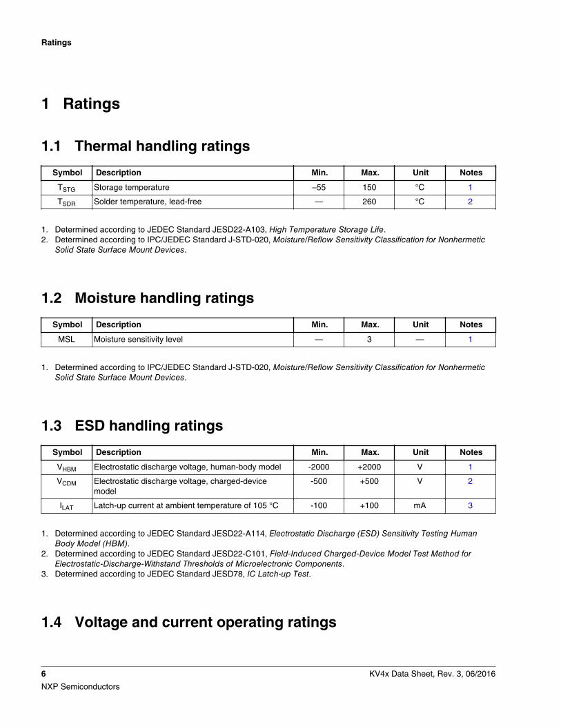
1 Ratings
1.1 Thermal handling ratings
Symbol Description Min. Max. Unit Notes
TSTG Storage temperature –55 150 °C 1
TSDR Solder temperature, lead-free — 260 °C 2
1. Determined according to JEDEC Standard JESD22-A103, High Temperature Storage Life.2. Determined according to IPC/JEDEC Standard J-STD-020, Moisture/Reflow Sensitivity Classification for Nonhermetic
Solid State Surface Mount Devices.
1.2 Moisture handling ratings
Symbol Description Min. Max. Unit Notes
MSL Moisture sensitivity level — 3 — 1
1. Determined according to IPC/JEDEC Standard J-STD-020, Moisture/Reflow Sensitivity Classification for NonhermeticSolid State Surface Mount Devices.
1.3 ESD handling ratings
Symbol Description Min. Max. Unit Notes
VHBM Electrostatic discharge voltage, human-body model -2000 +2000 V 1
VCDM Electrostatic discharge voltage, charged-devicemodel
-500 +500 V 2
ILAT Latch-up current at ambient temperature of 105 °C -100 +100 mA 3
1. Determined according to JEDEC Standard JESD22-A114, Electrostatic Discharge (ESD) Sensitivity Testing HumanBody Model (HBM).
2. Determined according to JEDEC Standard JESD22-C101, Field-Induced Charged-Device Model Test Method forElectrostatic-Discharge-Withstand Thresholds of Microelectronic Components.
3. Determined according to JEDEC Standard JESD78, IC Latch-up Test.
1.4 Voltage and current operating ratings
Ratings
6 KV4x Data Sheet, Rev. 3, 06/2016
NXP Semiconductors
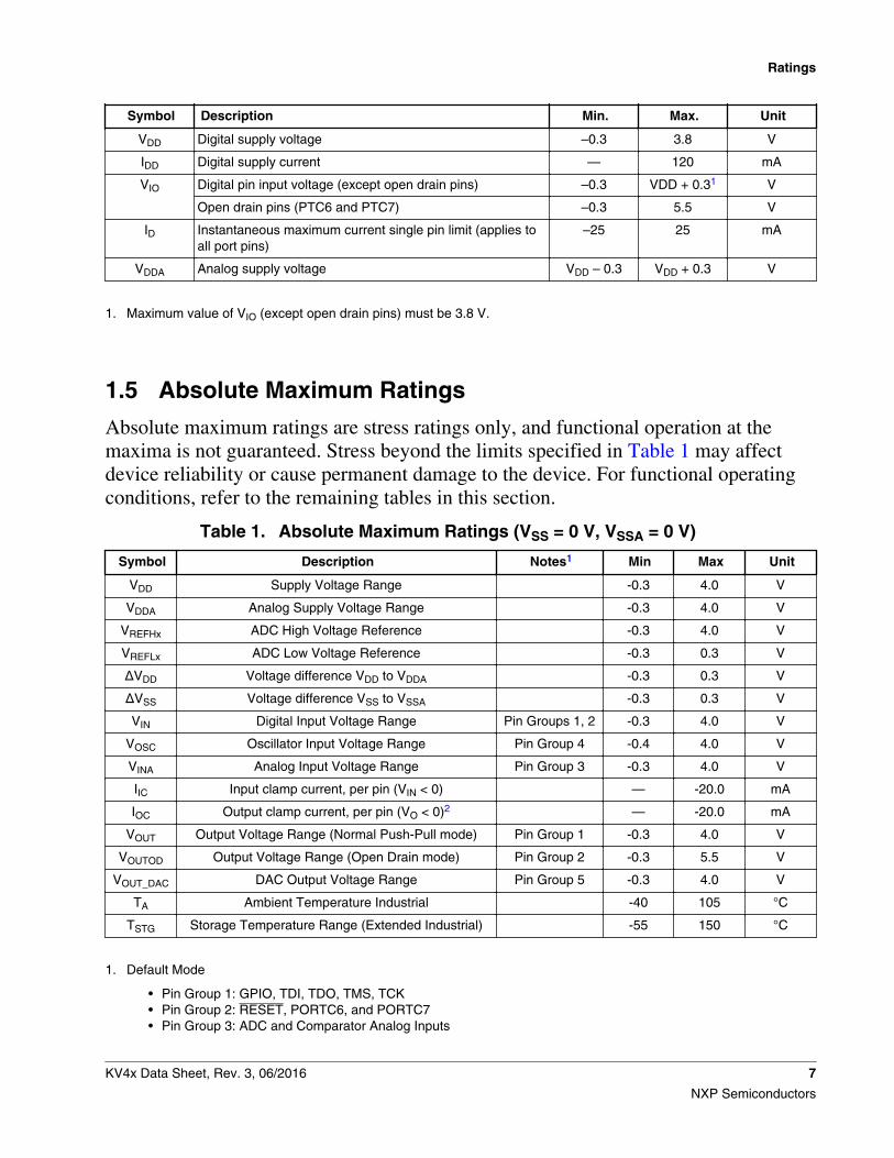
Symbol Description Min. Max. Unit
VDD Digital supply voltage –0.3 3.8 V
IDD Digital supply current — 120 mA
VIO Digital pin input voltage (except open drain pins) –0.3 VDD + 0.31 V
Open drain pins (PTC6 and PTC7) –0.3 5.5 V
ID Instantaneous maximum current single pin limit (applies toall port pins)
–25 25 mA
VDDA Analog supply voltage VDD – 0.3 VDD + 0.3 V
1. Maximum value of VIO (except open drain pins) must be 3.8 V.
1.5 Absolute Maximum Ratings
Absolute maximum ratings are stress ratings only, and functional operation at themaxima is not guaranteed. Stress beyond the limits specified in Table 1 may affectdevice reliability or cause permanent damage to the device. For functional operatingconditions, refer to the remaining tables in this section.
Table 1. Absolute Maximum Ratings (VSS = 0 V, VSSA = 0 V)
Symbol Description Notes1 Min Max Unit
VDD Supply Voltage Range -0.3 4.0 V
VDDA Analog Supply Voltage Range -0.3 4.0 V
VREFHx ADC High Voltage Reference -0.3 4.0 V
VREFLx ADC Low Voltage Reference -0.3 0.3 V
ΔVDD Voltage difference VDD to VDDA -0.3 0.3 V
ΔVSS Voltage difference VSS to VSSA -0.3 0.3 V
VIN Digital Input Voltage Range Pin Groups 1, 2 -0.3 4.0 V
VOSC Oscillator Input Voltage Range Pin Group 4 -0.4 4.0 V
VINA Analog Input Voltage Range Pin Group 3 -0.3 4.0 V
IIC Input clamp current, per pin (VIN < 0) — -20.0 mA
IOC Output clamp current, per pin (VO < 0)2 — -20.0 mA
VOUT Output Voltage Range (Normal Push-Pull mode) Pin Group 1 -0.3 4.0 V
VOUTOD Output Voltage Range (Open Drain mode) Pin Group 2 -0.3 5.5 V
VOUT_DAC DAC Output Voltage Range Pin Group 5 -0.3 4.0 V
TA Ambient Temperature Industrial -40 105 °C
TSTG Storage Temperature Range (Extended Industrial) -55 150 °C
1. Default Mode
• Pin Group 1: GPIO, TDI, TDO, TMS, TCK• Pin Group 2: RESET, PORTC6, and PORTC7• Pin Group 3: ADC and Comparator Analog Inputs
Ratings
KV4x Data Sheet, Rev. 3, 06/2016 7
NXP Semiconductors
• Pin Group 4: XTAL, EXTAL• Pin Group 5: DAC analog output
2. Continuous clamp current per pin is -2.0 mA
2 GeneralElectromagnetic compatibility (EMC) performance depends on the environment inwhich the MCU resides. Board design and layout, circuit topology choices, location,characteristics of external components, and MCU software operation play a significantrole in EMC performance.
See the following applications notes available on nxp.com for guidelines on optimizingEMC performance.
• AN2321: Designing for Board Level Electromagnetic Compatibility• AN1050: Designing for Electromagnetic Compatibility (EMC) with HCMOS
Microcontrollers• AN1263: Designing for Electromagnetic Compatibility with Single-Chip
Microcontrollers• AN2764: Improving the Transient Immunity Performance of Microcontroller-Based
Applications• AN1259: System Design and Layout Techniques for Noise Reduction in MCU-
Based Systems
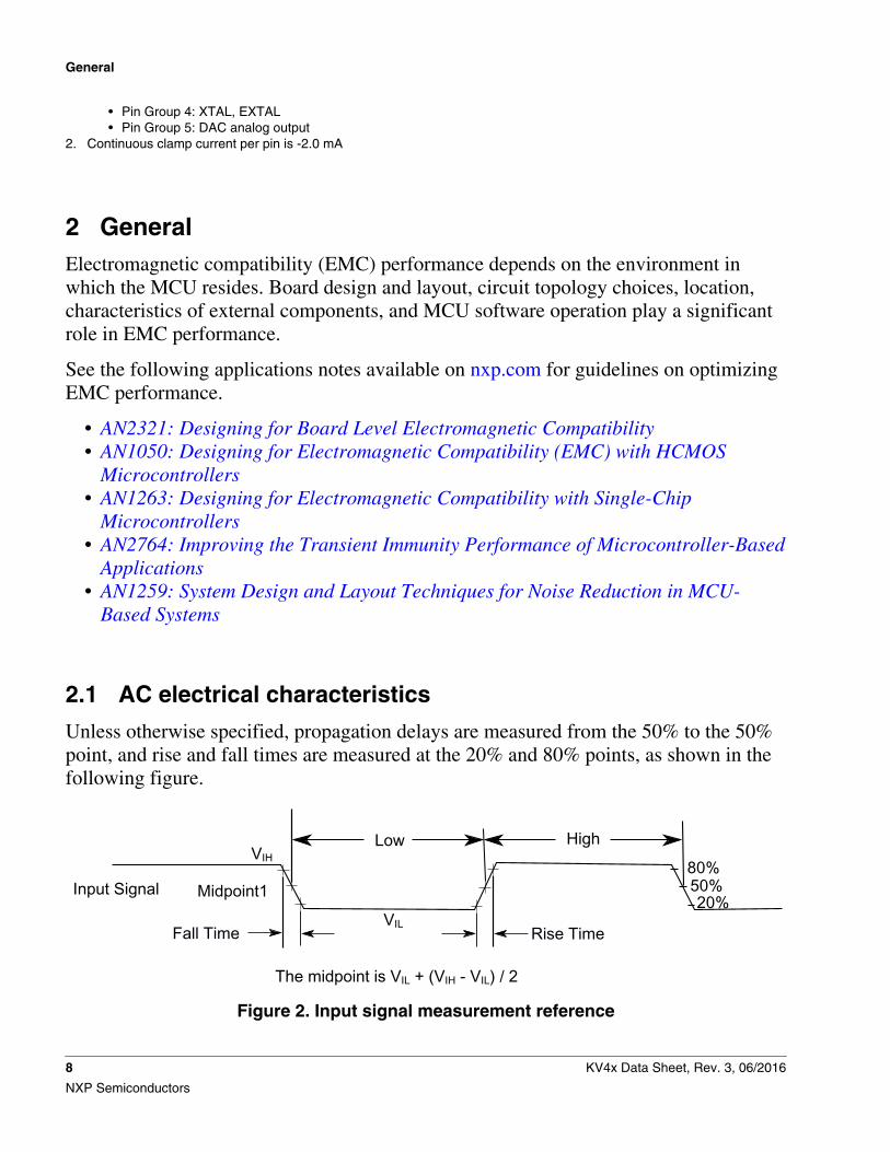
2.1 AC electrical characteristics
Unless otherwise specified, propagation delays are measured from the 50% to the 50%point, and rise and fall times are measured at the 20% and 80% points, as shown in thefollowing figure.
80%
20%50%
VIL
Input Signal
VIH
Fall Time
HighLow
Rise Time
Midpoint1
The midpoint is VIL + (VIH - VIL) / 2
Figure 2. Input signal measurement reference
General
8 KV4x Data Sheet, Rev. 3, 06/2016
NXP Semiconductors
All digital I/O switching characteristics, unless otherwise specified, assume:1. output pins
• have CL=30pF loads,• are slew rate disabled, and• are normal drive strength
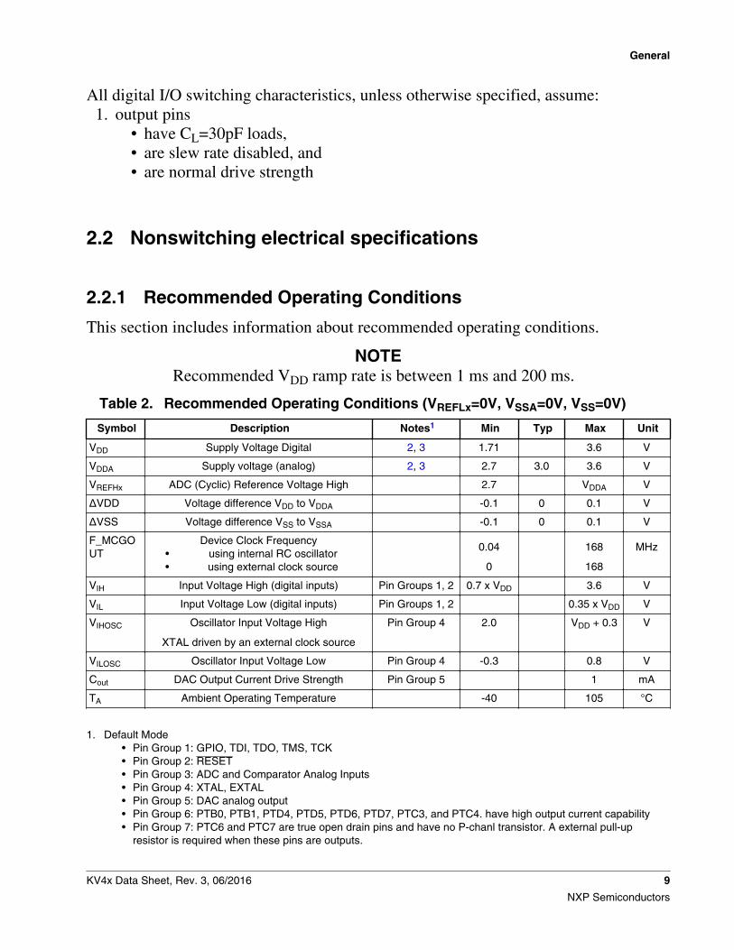
2.2 Nonswitching electrical specifications
2.2.1 Recommended Operating Conditions
This section includes information about recommended operating conditions.
NOTERecommended VDD ramp rate is between 1 ms and 200 ms.
Table 2. Recommended Operating Conditions (VREFLx=0V, VSSA=0V, VSS=0V)
Symbol Description Notes1 Min Typ Max Unit
VDD Supply Voltage Digital 2, 3 1.71 3.6 V
VDDA Supply voltage (analog) 2, 3 2.7 3.0 3.6 V
VREFHx ADC (Cyclic) Reference Voltage High 2.7 VDDA V
ΔVDD Voltage difference VDD to VDDA -0.1 0 0.1 V
ΔVSS Voltage difference VSS to VSSA -0.1 0 0.1 V
F_MCGOUT
Device Clock Frequency• using internal RC oscillator• using external clock source
0.04
0
168
168
MHz
VIH Input Voltage High (digital inputs) Pin Groups 1, 2 0.7 x VDD 3.6 V
VIL Input Voltage Low (digital inputs) Pin Groups 1, 2 0.35 x VDD V
VIHOSC Oscillator Input Voltage High
XTAL driven by an external clock source
Pin Group 4 2.0 VDD + 0.3 V
VILOSC Oscillator Input Voltage Low Pin Group 4 -0.3 0.8 V
Cout DAC Output Current Drive Strength Pin Group 5 1 mA
TA Ambient Operating Temperature -40 105 °C
1. Default Mode• Pin Group 1: GPIO, TDI, TDO, TMS, TCK• Pin Group 2: RESET• Pin Group 3: ADC and Comparator Analog Inputs• Pin Group 4: XTAL, EXTAL• Pin Group 5: DAC analog output• Pin Group 6: PTB0, PTB1, PTD4, PTD5, PTD6, PTD7, PTC3, and PTC4. have high output current capability• Pin Group 7: PTC6 and PTC7 are true open drain pins and have no P-chanl transistor. A external pull-up
resistor is required when these pins are outputs.
General
KV4x Data Sheet, Rev. 3, 06/2016 9
NXP Semiconductors
2. If the ADC is enabled, minimum VDD is 2.7 V and minimum VDDA is 2.7 V. ADCA and ADCB are not guaranteed tooperate below 2.7 V. All other analog modules besides the ADC and Nano-edge will operate down to 1.71 V.
3. If the Nano-edge is enabled, minimum VDD is 3.0 V and minimum VDDA is 3.0 V. Nano-edge is not guaranteed to operatebelow 3.0 V. All other analog modules besides the ADC and Nano-edge will operate down to 1.71 V.
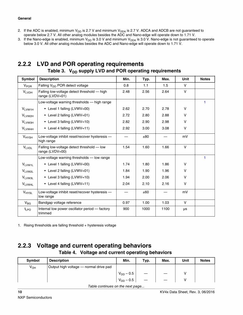
2.2.2 LVD and POR operating requirementsTable 3. VDD supply LVD and POR operating requirements
Symbol Description Min. Typ. Max. Unit Notes
VPOR Falling VDD POR detect voltage 0.8 1.1 1.5 V
VLVDH Falling low-voltage detect threshold — highrange (LVDV=01)
2.48 2.56 2.64 V
VLVW1H
VLVW2H
VLVW3H
VLVW4H
Low-voltage warning thresholds — high range
• Level 1 falling (LVWV=00)
• Level 2 falling (LVWV=01)
• Level 3 falling (LVWV=10)
• Level 4 falling (LVWV=11)
2.62
2.72
2.82
2.92
2.70
2.80
2.90
3.00
2.78
2.88
2.98
3.08
V
V
V
V
1
VHYSH Low-voltage inhibit reset/recover hysteresis —high range
— ±80 — mV
VLVDL Falling low-voltage detect threshold — lowrange (LVDV=00)
1.54 1.60 1.66 V
VLVW1L
VLVW2L
VLVW3L
VLVW4L
Low-voltage warning thresholds — low range
• Level 1 falling (LVWV=00)
• Level 2 falling (LVWV=01)
• Level 3 falling (LVWV=10)
• Level 4 falling (LVWV=11)
1.74
1.84
1.94
2.04
1.80
1.90
2.00
2.10
1.86
1.96
2.06
2.16
V
V
V
V
1
VHYSL Low-voltage inhibit reset/recover hysteresis —low range
— ±60 — mV
VBG Bandgap voltage reference 0.97 1.00 1.03 V
tLPO Internal low power oscillator period — factorytrimmed
900 1000 1100 μs
1. Rising thresholds are falling threshold + hysteresis voltage
2.2.3 Voltage and current operating behaviorsTable 4. Voltage and current operating behaviors
Symbol Description Min. Typ. Max. Unit Notes
VOH Output high voltage — normal drive pad
VDD – 0.5
VDD – 0.5
—
—
—
—
V
V
Table continues on the next page...
General
10 KV4x Data Sheet, Rev. 3, 06/2016
NXP Semiconductors
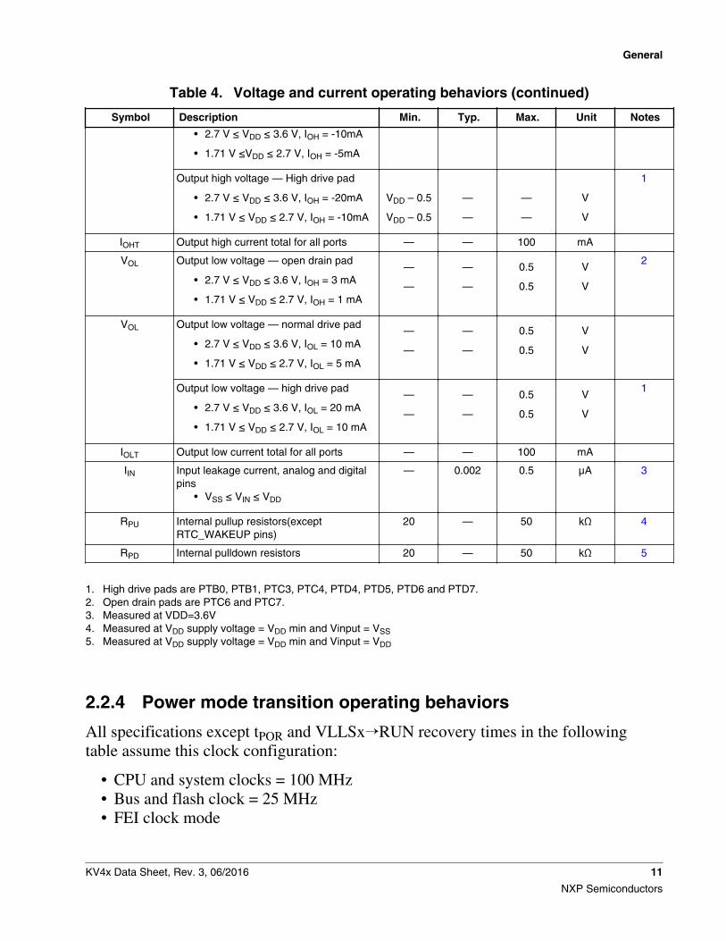
Table 4. Voltage and current operating behaviors (continued)
Symbol Description Min. Typ. Max. Unit Notes
• 2.7 V ≤ VDD ≤ 3.6 V, IOH = -10mA
• 1.71 V ≤VDD ≤ 2.7 V, IOH = -5mA
Output high voltage — High drive pad
• 2.7 V ≤ VDD ≤ 3.6 V, IOH = -20mA
• 1.71 V ≤ VDD ≤ 2.7 V, IOH = -10mA
VDD – 0.5
VDD – 0.5
—
—
—
—
V
V
1
IOHT Output high current total for all ports — — 100 mA
VOL Output low voltage — open drain pad
• 2.7 V ≤ VDD ≤ 3.6 V, IOH = 3 mA
• 1.71 V ≤ VDD ≤ 2.7 V, IOH = 1 mA
—
—
—
—
0.5
0.5
V
V
2
VOL Output low voltage — normal drive pad
• 2.7 V ≤ VDD ≤ 3.6 V, IOL = 10 mA
• 1.71 V ≤ VDD ≤ 2.7 V, IOL = 5 mA
—
—
—
—
0.5
0.5
V
V
Output low voltage — high drive pad
• 2.7 V ≤ VDD ≤ 3.6 V, IOL = 20 mA
• 1.71 V ≤ VDD ≤ 2.7 V, IOL = 10 mA
—
—
—
—
0.5
0.5
V
V
1
IOLT Output low current total for all ports — — 100 mA
IIN Input leakage current, analog and digitalpins
• VSS ≤ VIN ≤ VDD
— 0.002 0.5 µA 3
RPU Internal pullup resistors(exceptRTC_WAKEUP pins)
20 — 50 kΩ 4
RPD Internal pulldown resistors 20 — 50 kΩ 5
1. High drive pads are PTB0, PTB1, PTC3, PTC4, PTD4, PTD5, PTD6 and PTD7.2. Open drain pads are PTC6 and PTC7.3. Measured at VDD=3.6V4. Measured at VDD supply voltage = VDD min and Vinput = VSS5. Measured at VDD supply voltage = VDD min and Vinput = VDD
2.2.4 Power mode transition operating behaviors
All specifications except tPOR and VLLSx→RUN recovery times in the followingtable assume this clock configuration:
• CPU and system clocks = 100 MHz• Bus and flash clock = 25 MHz• FEI clock mode
General
KV4x Data Sheet, Rev. 3, 06/2016 11
NXP Semiconductors
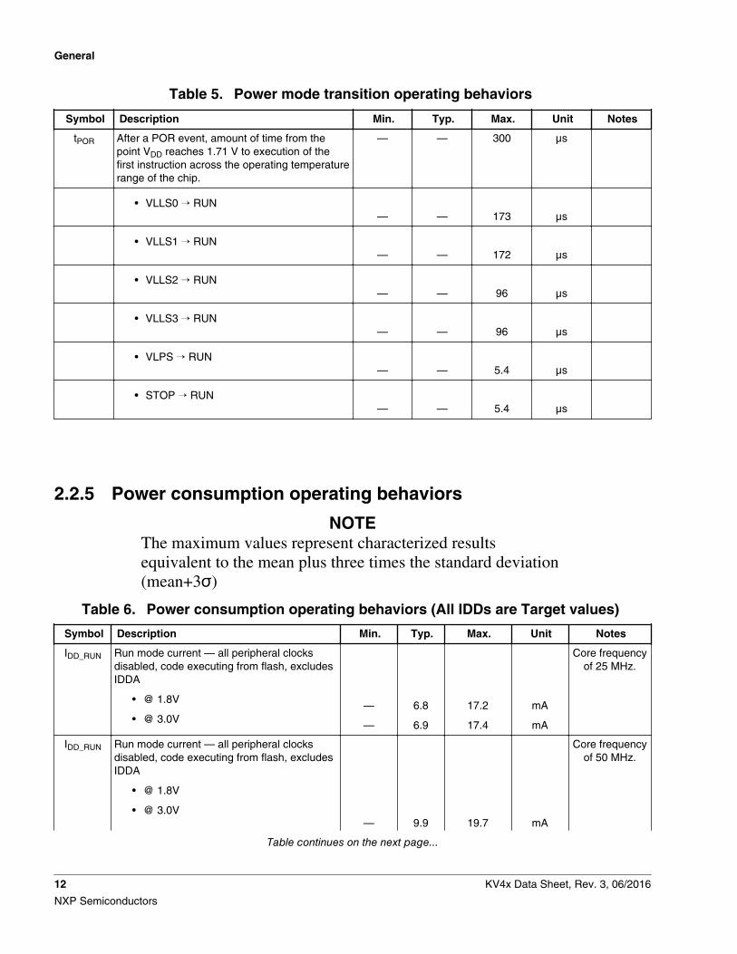
Table 5. Power mode transition operating behaviors
Symbol Description Min. Typ. Max. Unit Notes
tPOR After a POR event, amount of time from thepoint VDD reaches 1.71 V to execution of thefirst instruction across the operating temperaturerange of the chip.
— — 300 μs
• VLLS0 → RUN
—
—
173
μs
• VLLS1 → RUN
—
—
172
μs
• VLLS2 → RUN
—
—
96
μs
• VLLS3 → RUN
—
—
96
μs
• VLPS → RUN
—
—
5.4
μs
• STOP → RUN
—
—
5.4
μs
2.2.5 Power consumption operating behaviors
NOTEThe maximum values represent characterized resultsequivalent to the mean plus three times the standard deviation(mean+3σ)
Table 6. Power consumption operating behaviors (All IDDs are Target values)
Symbol Description Min. Typ. Max. Unit Notes
IDD_RUN Run mode current — all peripheral clocksdisabled, code executing from flash, excludesIDDA
• @ 1.8V
• @ 3.0V
—
—
6.8
6.9
17.2
17.4
mA
mA
Core frequencyof 25 MHz.
IDD_RUN Run mode current — all peripheral clocksdisabled, code executing from flash, excludesIDDA
• @ 1.8V
• @ 3.0V
—
9.9
19.7
mA
Core frequencyof 50 MHz.
Table continues on the next page...
General
12 KV4x Data Sheet, Rev. 3, 06/2016
NXP Semiconductors
Table 6. Power consumption operating behaviors (All IDDs are Target values) (continued)
Symbol Description Min. Typ. Max. Unit Notes
— 10.0 19.8 mA
IDD_RUN Run mode current — all peripheral clocksdisabled, code executing from flash, excludesIDDA
• @ 1.8V
• @ 3.0V
—
—
17.0
17.2
25.9
26.1
mA
mA
Core frequencyof 100 MHz.
IDD_HSRUN Run mode current — all peripheral clocksdisabled, code executing from flash, excludesIDDA
• @ 1.8V
• @ 3.0V
—
—
26.3
26.5
45.3
45.5
mA
mA
Core frequencyof 168 MHz.
IDD_HSRUN Run mode current — all peripheral clocksenabled, code executing from flash,excludesIDDA
• @ 3.0V
• @ 25°C
• @ 105°C
—
—
34.0
39.0
45.5
53.2
mA
mA
Core frequencyof 168 MHz.Nanoedge
module at 84MHz.
IDD_WAIT Wait mode high frequency current at 3.0 V —all peripheral clocks disabled
— 8.9 — mA
IDD_VLPR Very-low-power run mode current at 3.0 V —all peripheral clocks disabled
— 0.58 — mA Core frequencyof 4 Mhz.
IDD_VLPR Very-low-power run mode current at 3.0 V —all peripheral clocks enabled
— 0.83 — mA Core frequencyof 4 Mhz.
IDD_VLPW Very-low-power wait mode current at 3.0 V —all peripheral clocks disabled
— 0.34 — mA Bus frequencyof 2 MHz.
IDD_STOP Stop mode current at 3.0 V
• @ –40 to 25°C
• @ 70°C
• @ 105°C
—
—
—
0.43
1.16
3.05
2.03
4.27
10.13
mA
mA
mA
IDD_VLPS Very-low-power stop mode current at 3.0 V
• @ –40 to 25°C
• @ 70°C
• @ 105°C
—
—
—
58
280
924
218
1340
2870
μA
μA
μA
IDD_VLLS3 Very low-leakage stop mode 3 current at 3.0 V
• @ –40 to 25°C
• @ 70°C
• @ 105°C
—
—
—
2.8
9.6
37.4
5.3
35.1
134.8
μA
μA
μA
IDD_VLLS2 Very low-leakage stop mode 2 current at 3.0 V
Table continues on the next page...
General
KV4x Data Sheet, Rev. 3, 06/2016 13
NXP Semiconductors
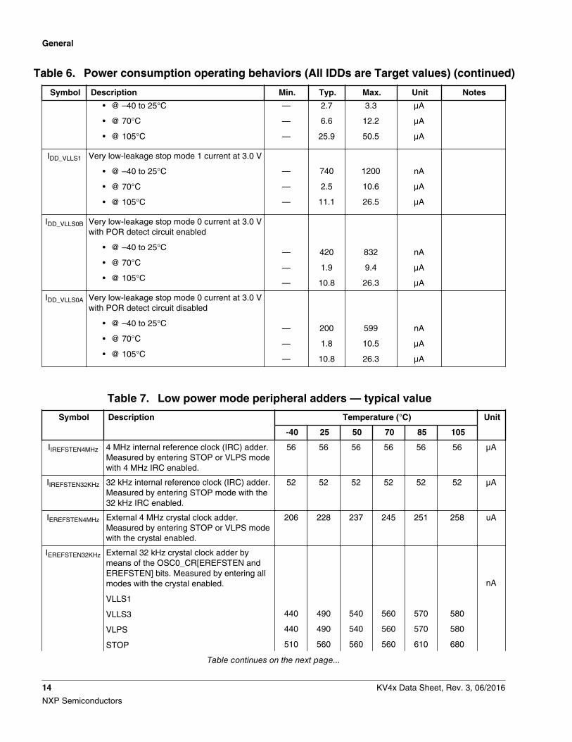
Table 6. Power consumption operating behaviors (All IDDs are Target values) (continued)
Symbol Description Min. Typ. Max. Unit Notes
• @ –40 to 25°C
• @ 70°C
• @ 105°C
—
—
—
2.7
6.6
25.9
3.3
12.2
50.5
μA
μA
μA
IDD_VLLS1 Very low-leakage stop mode 1 current at 3.0 V
• @ –40 to 25°C
• @ 70°C
• @ 105°C
—
—
—
740
2.5
11.1
1200
10.6
26.5
nA
μA
μA
IDD_VLLS0B Very low-leakage stop mode 0 current at 3.0 Vwith POR detect circuit enabled
• @ –40 to 25°C
• @ 70°C
• @ 105°C
—
—
—
420
1.9
10.8
832
9.4
26.3
nA
μA
μA
IDD_VLLS0A Very low-leakage stop mode 0 current at 3.0 Vwith POR detect circuit disabled
• @ –40 to 25°C
• @ 70°C
• @ 105°C
—
—
—
200
1.8
10.8
599
10.5
26.3
nA
μA
μA
Table 7. Low power mode peripheral adders — typical value
Symbol Description Temperature (°C) Unit
-40 25 50 70 85 105
IIREFSTEN4MHz 4 MHz internal reference clock (IRC) adder.Measured by entering STOP or VLPS modewith 4 MHz IRC enabled.
56 56 56 56 56 56 µA
IIREFSTEN32KHz 32 kHz internal reference clock (IRC) adder.Measured by entering STOP mode with the32 kHz IRC enabled.
52 52 52 52 52 52 µA
IEREFSTEN4MHz External 4 MHz crystal clock adder.Measured by entering STOP or VLPS modewith the crystal enabled.
206 228 237 245 251 258 uA
IEREFSTEN32KHz External 32 kHz crystal clock adder bymeans of the OSC0_CR[EREFSTEN andEREFSTEN] bits. Measured by entering allmodes with the crystal enabled.
VLLS1
VLLS3
VLPS
STOP
440
440
510
490
490
560
540
540
560
560
560
560
570
570
610
580
580
680
nA
Table continues on the next page...
General
14 KV4x Data Sheet, Rev. 3, 06/2016
NXP Semiconductors
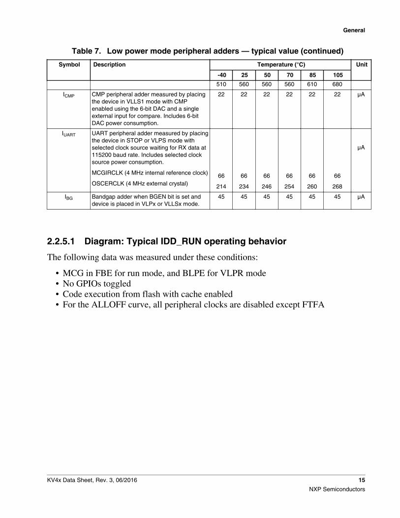
Table 7. Low power mode peripheral adders — typical value (continued)
Symbol Description Temperature (°C) Unit
-40 25 50 70 85 105
510 560 560 560 610 680
ICMP CMP peripheral adder measured by placingthe device in VLLS1 mode with CMPenabled using the 6-bit DAC and a singleexternal input for compare. Includes 6-bitDAC power consumption.
22 22 22 22 22 22 µA
IUART UART peripheral adder measured by placingthe device in STOP or VLPS mode withselected clock source waiting for RX data at115200 baud rate. Includes selected clocksource power consumption.
MCGIRCLK (4 MHz internal reference clock)
OSCERCLK (4 MHz external crystal)
66
214
66
234
66
246
66
254
66
260
66
268
µA
IBG Bandgap adder when BGEN bit is set anddevice is placed in VLPx or VLLSx mode.
45 45 45 45 45 45 µA
2.2.5.1 Diagram: Typical IDD_RUN operating behavior
The following data was measured under these conditions:
• MCG in FBE for run mode, and BLPE for VLPR mode• No GPIOs toggled• Code execution from flash with cache enabled• For the ALLOFF curve, all peripheral clocks are disabled except FTFA
General
KV4x Data Sheet, Rev. 3, 06/2016 15
NXP Semiconductors
Figure 3. Run mode supply current vs. core frequency
General
16 KV4x Data Sheet, Rev. 3, 06/2016
NXP Semiconductors
000.00E+00
100.00E-06
200.00E-06
300.00E-06
400.00E-06
500.00E-06
600.00E-06
700.00E-06
800.00E-06
900.00E-06
1.00E-03
'1-1-2 '1-1-1 '1-2-4 '1-1-4 '1-1-2 '1-2-4 '1-1-4
1 2 4
Curr
ent C
onsu
mpt
ion
on V
DD
(A)
Very Low Power Run (VLPR) Current vs Core Frequency
ALLOFF
ALLON
Temp (C)=25,VDD=3.6V,CACHE=ENABLE,Code Residence=Flash
All Peripheral Clk Gates
Clk RatioCore-Bus-Flash
Core Freq (Mhz)
Figure 4. VLPR mode current vs. core frequency
2.2.6 EMC radiated emissions operating behaviors
NOTEEMC measurements to IC-level IEC standards are availablefrom NXP on request.
Table 8. EMC radiated emissions operating behaviors
Symbol Description Frequencyband(MHz)
Typ. Unit Notes
VRE1 Radiated emissions voltage, band 1 0.15–50 20 dBμV 1, 2
VRE2 Radiated emissions voltage, band 2 50–150 18 dBμV
VRE3 Radiated emissions voltage, band 3 150–500 14 dBμV
VRE4 Radiated emissions voltage, band 4 500–1000 8 dBμV
VRE_IEC IEC level 0.15–1000 L — 2, 3
General
KV4x Data Sheet, Rev. 3, 06/2016 17
NXP Semiconductors
1. Determined according to IEC Standard 61967-1, Integrated Circuits - Measurement of Electromagnetic Emissions, 150kHz to 1 GHz Part 1: General Conditions and Definitions and IEC Standard 61967-2, Integrated Circuits - Measurementof Electromagnetic Emissions, 150 kHz to 1 GHz Part 2: Measurement of Radiated Emissions—TEM Cell andWideband TEM Cell Method. Measurements were made while the microcontroller was running basic application code.The reported emission level is the value of the maximum measured emission, rounded up to the next whole number,from among the measured orientations in each frequency range.
2. VDD = 3.3 V, TA = 25 °C, fOSC = 10 MHz (crystal), fSYS = 75 MHz, fBUS = 25 MHz3. Specified according to Annex D of IEC Standard 61967-2, Measurement of Radiated Emissions—TEM Cell and
Wideband TEM Cell Method
2.2.7 Designing with radiated emissions in mindTo find application notes that provide guidance on designing your system to minimizeinterference from radiated emissions:
1. Go to www.nxp.com.2. Perform a keyword search for “EMC design.”
2.2.8 Capacitance attributesTable 9. Capacitance attributes
Symbol Description Min. Max. Unit
CIN_A Input capacitance: analog pins — 7 pF
CIN_D Input capacitance: digital pins — 7 pF
2.3 Switching specifications
2.3.1 Typical device clock specificationsTable 10. Typical device clock specifications
Symbol Description Min. Max. Unit Notes
High Speed RUN mode
fSYS System and core clock — 168 MHz
fBUS Bus and Flash clock — 24 MHz
fFPCK Fast peripheral clock — 84 MHz
fNANO Nano-edge clock — 168 MHz
Normal run mode
fSYS System and core clock — 100 MHz
fBUS Bus and Flash clock — 25 MHz
Table continues on the next page...
General
18 KV4x Data Sheet, Rev. 3, 06/2016
NXP Semiconductors
Table 10. Typical device clock specifications (continued)
Symbol Description Min. Max. Unit Notes
fFPCK Fast peripheral clock — 100 MHz
fNANO Nano-edge clock — 200 MHz
Low Speed RUN mode
fSYS System and core clock — 50 MHz
fBUS Bus and Flash clock — 25 MHz
fFPCK Fast peripheral clock — 100 MHz
fNANO Nano-edge clock — 200 MHz
NOTEWhen NaneEdge circuit is enabled, the following clock setmust be followed:
1. NanoEdge clock source must be from the PLL output2. NanoEdge clock must be 2x the fast peripheral clock3. NanoEdge clock must in the range of 164 Mhz ~232
Mhz
2.3.2 General switching specifications
These general purpose specifications apply to all signals configured for GPIO, UART,and I2C signals.
Table 11. General switching specifications
Symbol Description Min. Max. Unit Notes
GPIO pin interrupt pulse width (digital glitch filterdisabled) — Synchronous path
1.5 — Bus clockcycles
1
External RESET and NMI pin interrupt pulse width —Asynchronous path
100 — ns 2
GPIO pin interrupt pulse width — Asynchronous path 16 — ns 2
Port rise and fall time
Fast slew rate
1.71≤ VDD ≤ 2.7 V
2.7 ≤ VDD ≤ 3.6 V
—
—
8
7
ns
ns
3
Port rise and fall time
Slow slew rate
1.71≤ VDD ≤ 2.7 V
2.7 ≤ VDD ≤ 3.6 V
—
—
25
15
ns
ns
General
KV4x Data Sheet, Rev. 3, 06/2016 19
NXP Semiconductors
1. The greater synchronous and asynchronous timing must be met.2. This is the shortest pulse that is guaranteed to be recognized.3. For high drive pins with high drive enabled, load is 75pF; other pins load (low drive) is 25pF.
2.4 Thermal specifications
2.4.1 Thermal operating requirementsTable 12. Thermal operating requirements
Symbol Description Min. Max. Unit
TJ Die junction temperature –40 125 °C
TA Ambient temperature –40 105 °C
2.4.2 Thermal attributesTable 13. Thermal attributes
Board type Symbol Description 100LQFP
64 LQFP 48 LQFP Unit Notes
Single-layer (1S) RθJA Thermal resistance, junction toambient (natural convection)
62 64 71 °C/W 1
Four-layer (2s2p) RθJA Thermal resistance, junction toambient (natural convection)
49 46 47 °C/W
Single-layer (1S) RθJMA Thermal resistance, junction toambient (200 ft./min. air speed)
52 52 58 °C/W
Four-layer (2s2p) RθJMA Thermal resistance, junction toambient (200 ft./min. air speed)
43 39 41 °C/W
— RθJB Thermal resistance, junction toboard
35 28 24 °C/W 2
— RθJC Thermal resistance, junction tocase
17 15 18 °C/W 3
— ΨJT Thermal characterizationparameter, junction to packagetop outside center (naturalconvection)
3 2 2 °C/W 4
1. Determined according to JEDEC Standard JESD51-2, Integrated Circuits Thermal Test Method EnvironmentalConditions—Natural Convection (Still Air), or EIA/JEDEC Standard JESD51-6, Integrated Circuit Thermal Test MethodEnvironmental Conditions—Forced Convection (Moving Air).
2. Determined according to JEDEC Standard JESD51-8, Integrated Circuit Thermal Test Method EnvironmentalConditions—Junction-to-Board.
3. Determined according to Method 1012.1 of MIL-STD 883, Test Method Standard, Microcircuits, with the cold platetemperature used for the case temperature. The value includes the thermal resistance of the interface material betweenthe top of the package and the cold plate.
General
20 KV4x Data Sheet, Rev. 3, 06/2016
NXP Semiconductors

4. Determined according to JEDEC Standard JESD51-2, Integrated Circuits Thermal Test Method EnvironmentalConditions—Natural Convection (Still Air).
3 Peripheral operating requirements and behaviors
3.1 Core modules
3.1.1 SWD ElectricalsTable 14. SWD full voltage range electricals
Symbol Description Min. Max. Unit
Operating voltage 1.71 3.6 V
J1 SWD_CLK frequency of operation
• Serial wire debug
0
25
MHz
J2 SWD_CLK cycle period 1/J1 — ns
J3 SWD_CLK clock pulse width
• Serial wire debug
20
—
ns
J4 SWD_CLK rise and fall times — 3 ns
J9 SWD_DIO input data setup time to SWD_CLK rise 10 — ns
J10 SWD_DIO input data hold time after SWD_CLK rise 0 — ns
J11 SWD_CLK high to SWD_DIO data valid — 32 ns
J12 SWD_CLK high to SWD_DIO high-Z 5 — ns
J2J3 J3
J4 J4
SWD_CLK (input)
Figure 5. Serial wire clock input timing
Peripheral operating requirements and behaviors
KV4x Data Sheet, Rev. 3, 06/2016 21
NXP Semiconductors
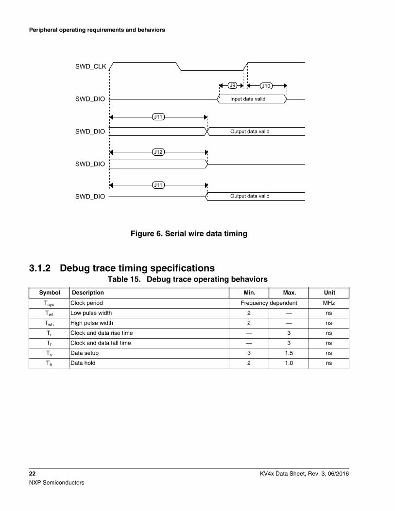
J11
J12
J11
J9 J10
Input data valid
Output data valid
Output data valid
SWD_CLK
SWD_DIO
SWD_DIO
SWD_DIO
SWD_DIO
Figure 6. Serial wire data timing
3.1.2 Debug trace timing specificationsTable 15. Debug trace operating behaviors
Symbol Description Min. Max. Unit
Tcyc Clock period Frequency dependent MHz
Twl Low pulse width 2 — ns
Twh High pulse width 2 — ns
Tr Clock and data rise time — 3 ns
Tf Clock and data fall time — 3 ns
Ts Data setup 3 1.5 ns
Th Data hold 2 1.0 ns
Peripheral operating requirements and behaviors
22 KV4x Data Sheet, Rev. 3, 06/2016
NXP Semiconductors
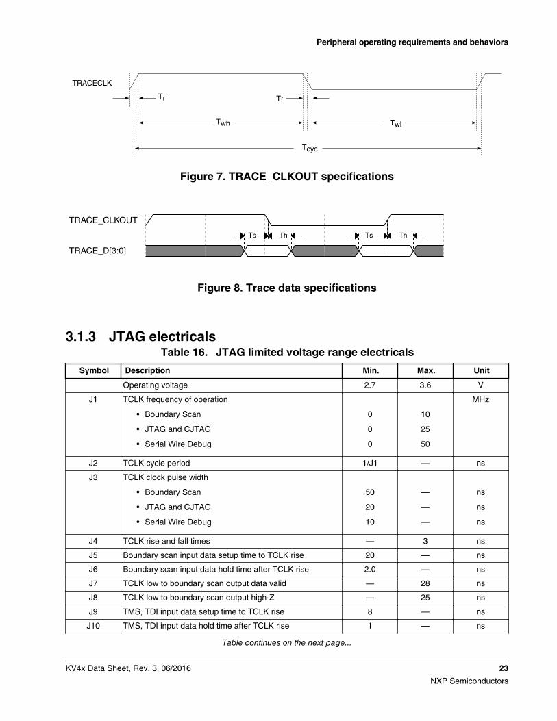
TRACECLK
Tr
Twh
Tf
Tcyc
Twl
Figure 7. TRACE_CLKOUT specifications
ThTs Ts Th
TRACE_CLKOUT
TRACE_D[3:0]
Figure 8. Trace data specifications
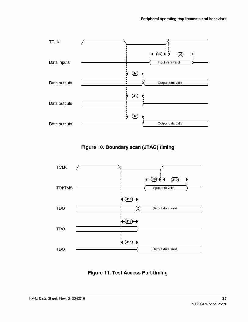
3.1.3 JTAG electricalsTable 16. JTAG limited voltage range electricals
Symbol Description Min. Max. Unit
Operating voltage 2.7 3.6 V
J1 TCLK frequency of operation
• Boundary Scan
• JTAG and CJTAG
• Serial Wire Debug
0
0
0
10
25
50
MHz
J2 TCLK cycle period 1/J1 — ns
J3 TCLK clock pulse width
• Boundary Scan
• JTAG and CJTAG
• Serial Wire Debug
50
20
10
—
—
—
ns
ns
ns
J4 TCLK rise and fall times — 3 ns
J5 Boundary scan input data setup time to TCLK rise 20 — ns
J6 Boundary scan input data hold time after TCLK rise 2.0 — ns
J7 TCLK low to boundary scan output data valid — 28 ns
J8 TCLK low to boundary scan output high-Z — 25 ns
J9 TMS, TDI input data setup time to TCLK rise 8 — ns
J10 TMS, TDI input data hold time after TCLK rise 1 — ns
Table continues on the next page...
Peripheral operating requirements and behaviors
KV4x Data Sheet, Rev. 3, 06/2016 23
NXP Semiconductors
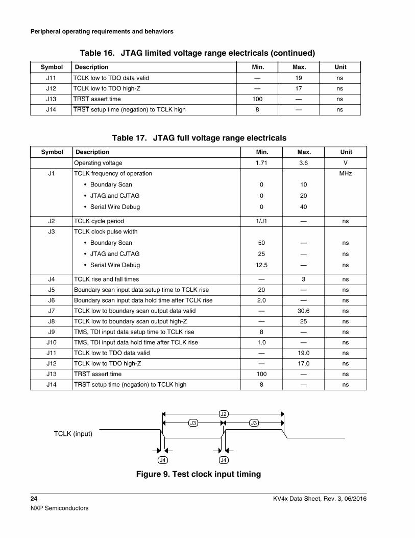
Table 16. JTAG limited voltage range electricals (continued)
Symbol Description Min. Max. Unit
J11 TCLK low to TDO data valid — 19 ns
J12 TCLK low to TDO high-Z — 17 ns
J13 TRST assert time 100 — ns
J14 TRST setup time (negation) to TCLK high 8 — ns
Table 17. JTAG full voltage range electricals
Symbol Description Min. Max. Unit
Operating voltage 1.71 3.6 V
J1 TCLK frequency of operation
• Boundary Scan
• JTAG and CJTAG
• Serial Wire Debug
0
0
0
10
20
40
MHz
J2 TCLK cycle period 1/J1 — ns
J3 TCLK clock pulse width
• Boundary Scan
• JTAG and CJTAG
• Serial Wire Debug
50
25
12.5
—
—
—
ns
ns
ns
J4 TCLK rise and fall times — 3 ns
J5 Boundary scan input data setup time to TCLK rise 20 — ns
J6 Boundary scan input data hold time after TCLK rise 2.0 — ns
J7 TCLK low to boundary scan output data valid — 30.6 ns
J8 TCLK low to boundary scan output high-Z — 25 ns
J9 TMS, TDI input data setup time to TCLK rise 8 — ns
J10 TMS, TDI input data hold time after TCLK rise 1.0 — ns
J11 TCLK low to TDO data valid — 19.0 ns
J12 TCLK low to TDO high-Z — 17.0 ns
J13 TRST assert time 100 — ns
J14 TRST setup time (negation) to TCLK high 8 — ns
J2J3 J3
J4 J4
TCLK (input)
Figure 9. Test clock input timing
Peripheral operating requirements and behaviors
24 KV4x Data Sheet, Rev. 3, 06/2016
NXP Semiconductors
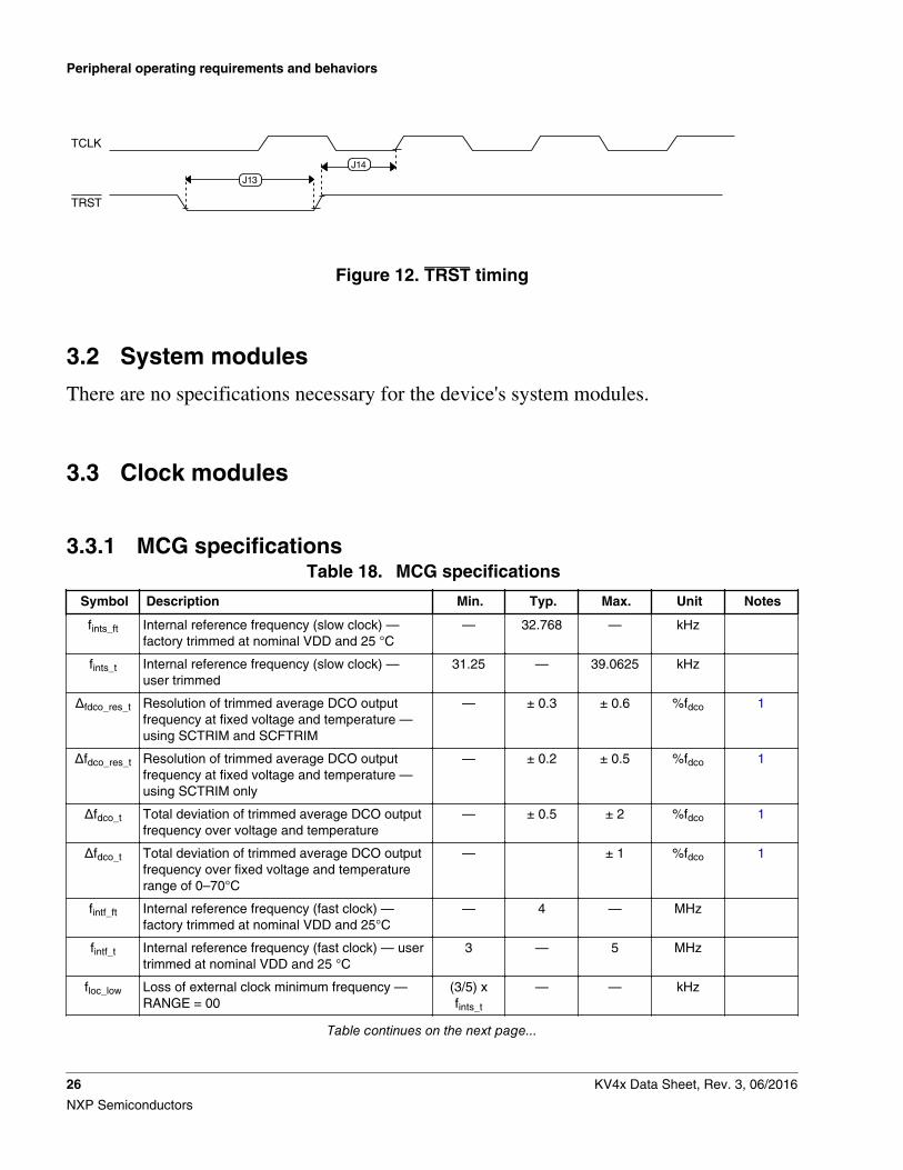
J7
J8
J7
J5 J6
Input data valid
Output data valid
Output data valid
TCLK
Data inputs
Data outputs
Data outputs
Data outputs
Figure 10. Boundary scan (JTAG) timing
J11
J12
J11
J9 J10
Input data valid
Output data valid
Output data valid
TCLK
TDI/TMS
TDO
TDO
TDO
Figure 11. Test Access Port timing
Peripheral operating requirements and behaviors
KV4x Data Sheet, Rev. 3, 06/2016 25
NXP Semiconductors
J14
J13
TCLK
TRST
Figure 12. TRST timing
3.2 System modules
There are no specifications necessary for the device's system modules.
3.3 Clock modules
3.3.1 MCG specificationsTable 18. MCG specifications
Symbol Description Min. Typ. Max. Unit Notes
fints_ft Internal reference frequency (slow clock) —factory trimmed at nominal VDD and 25 °C
— 32.768 — kHz
fints_t Internal reference frequency (slow clock) —user trimmed
31.25 — 39.0625 kHz
Δfdco_res_t Resolution of trimmed average DCO outputfrequency at fixed voltage and temperature —using SCTRIM and SCFTRIM
— ± 0.3 ± 0.6 %fdco 1
Δfdco_res_t Resolution of trimmed average DCO outputfrequency at fixed voltage and temperature —using SCTRIM only
— ± 0.2 ± 0.5 %fdco 1
Δfdco_t Total deviation of trimmed average DCO outputfrequency over voltage and temperature
— ± 0.5 ± 2 %fdco 1
Δfdco_t Total deviation of trimmed average DCO outputfrequency over fixed voltage and temperaturerange of 0–70°C
— ± 1 %fdco 1
fintf_ft Internal reference frequency (fast clock) —factory trimmed at nominal VDD and 25°C
— 4 — MHz
fintf_t Internal reference frequency (fast clock) — usertrimmed at nominal VDD and 25 °C
3 — 5 MHz
floc_low Loss of external clock minimum frequency —RANGE = 00
(3/5) xfints_t
— — kHz
Table continues on the next page...
Peripheral operating requirements and behaviors
26 KV4x Data Sheet, Rev. 3, 06/2016
NXP Semiconductors
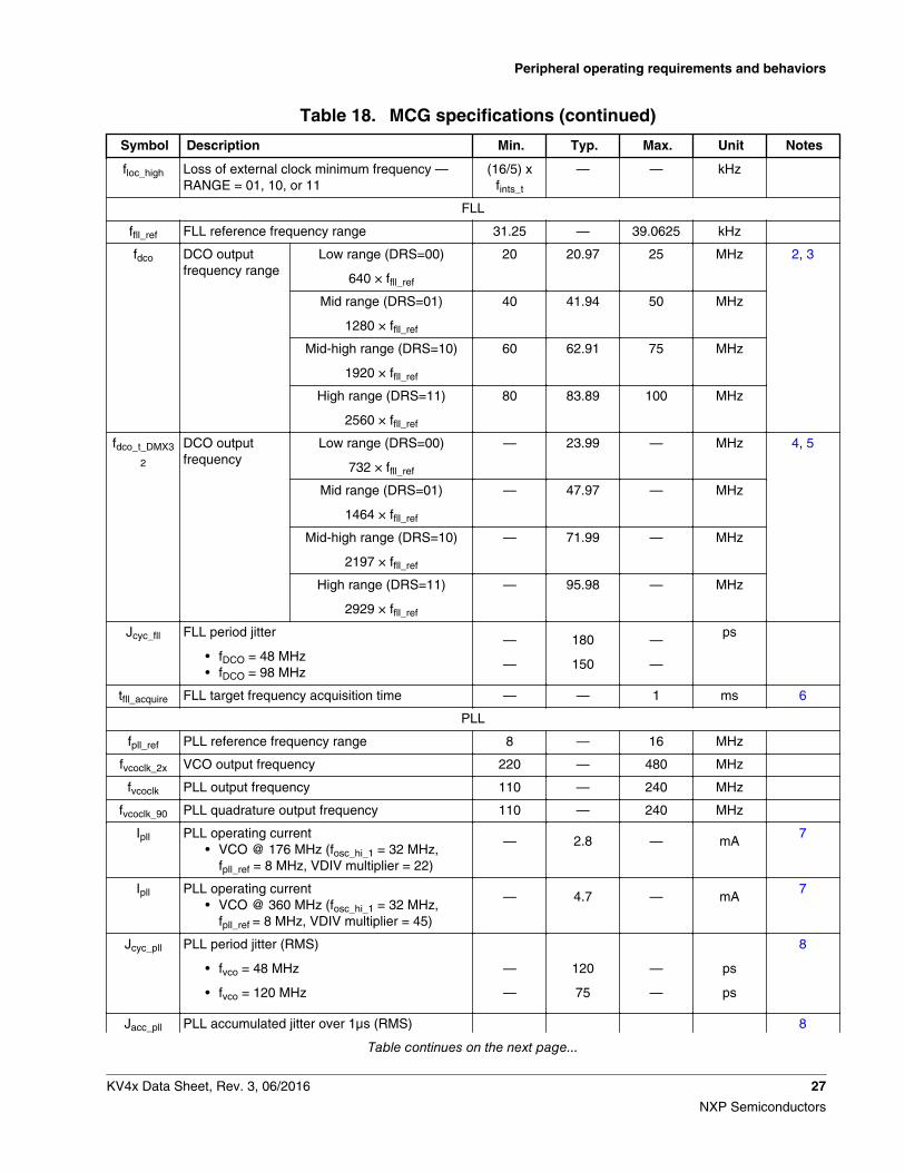
Table 18. MCG specifications (continued)
Symbol Description Min. Typ. Max. Unit Notes
floc_high Loss of external clock minimum frequency —RANGE = 01, 10, or 11
(16/5) xfints_t
— — kHz
FLL
ffll_ref FLL reference frequency range 31.25 — 39.0625 kHz
fdco DCO outputfrequency range
Low range (DRS=00)
640 × ffll_ref
20 20.97 25 MHz 2, 3
Mid range (DRS=01)
1280 × ffll_ref
40 41.94 50 MHz
Mid-high range (DRS=10)
1920 × ffll_ref
60 62.91 75 MHz
High range (DRS=11)
2560 × ffll_ref
80 83.89 100 MHz
fdco_t_DMX3
2
DCO outputfrequency
Low range (DRS=00)
732 × ffll_ref
— 23.99 — MHz 4, 5
Mid range (DRS=01)
1464 × ffll_ref
— 47.97 — MHz
Mid-high range (DRS=10)
2197 × ffll_ref
— 71.99 — MHz
High range (DRS=11)
2929 × ffll_ref
— 95.98 — MHz
Jcyc_fll FLL period jitter
• fDCO = 48 MHz• fDCO = 98 MHz
—
—
180
150
—
—
ps
tfll_acquire FLL target frequency acquisition time — — 1 ms 6
PLL
fpll_ref PLL reference frequency range 8 — 16 MHz
fvcoclk_2x VCO output frequency 220 — 480 MHz
fvcoclk PLL output frequency 110 — 240 MHz
fvcoclk_90 PLL quadrature output frequency 110 — 240 MHz
Ipll PLL operating current• VCO @ 176 MHz (fosc_hi_1 = 32 MHz,
fpll_ref = 8 MHz, VDIV multiplier = 22)
— 2.8 — mA7
Ipll PLL operating current• VCO @ 360 MHz (fosc_hi_1 = 32 MHz,
fpll_ref = 8 MHz, VDIV multiplier = 45)
— 4.7 — mA7
Jcyc_pll PLL period jitter (RMS)
• fvco = 48 MHz
• fvco = 120 MHz
—
—
120
75
—
—
ps
ps
8
Jacc_pll PLL accumulated jitter over 1µs (RMS) 8
Table continues on the next page...
Peripheral operating requirements and behaviors
KV4x Data Sheet, Rev. 3, 06/2016 27
NXP Semiconductors
Table 18. MCG specifications (continued)
Symbol Description Min. Typ. Max. Unit Notes
• fvco = 48 MHz
• fvco = 120 MHz
—
—
1350
600
—
—
ps
ps
Dunl Lock exit frequency tolerance ± 4.47 — ± 5.97 %
tpll_lock Lock detector detection time — — 150 × 10-6
+ 1075(1/fpll_ref)
s 9
1. This parameter is measured with the internal reference (slow clock) being used as a reference to the FLL (FEI clockmode).
2. These typical values listed are with the slow internal reference clock (FEI) using factory trim and DMX32=0.3. The resulting system clock frequencies should not exceed their maximum specified values. The DCO frequency
deviation (Δfdco_t) over voltage and temperature should be considered.4. These typical values listed are with the slow internal reference clock (FEI) using factory trim and DMX32=1.5. The resulting clock frequency must not exceed the maximum specified clock frequency of the device.6. This specification applies to any time the FLL reference source or reference divider is changed, trim value is changed,
DMX32 bit is changed, DRS bits are changed, or changing from FLL disabled (BLPE, BLPI) to FLL enabled (FEI, FEE,FBE, FBI). If a crystal/resonator is being used as the reference, this specification assumes it is already running.
7. Excludes any oscillator currents that are also consuming power while PLL is in operation.8. This specification was obtained using a NXP developed PCB. PLL jitter is dependent on the noise characteristics of
each PCB and results will vary.9. This specification applies to any time the PLL VCO divider or reference divider is changed, or changing from PLL
disabled (BLPE, BLPI) to PLL enabled (PBE, PEE). If a crystal/resonator is being used as the reference, thisspecification assumes it is already running.
3.3.2 Oscillator electrical specifications
3.3.2.1 Oscillator DC electrical specificationsTable 19. Oscillator DC electrical specifications
Symbol Description Min. Typ. Max. Unit Notes
VDD Supply voltage 1.71 — 3.6 V
IDDOSC Supply current — low-power mode (HGO=0)
• 32 kHz
• 4 MHz
• 8 MHz
• 16 MHz
• 24 MHz
• 32 MHz
—
—
—
—
—
—
500
200
300
950
1.2
1.5
—
—
—
—
—
—
nA
μA
μA
μA
mA
mA
1
IDDOSC Supply current — high gain mode (HGO=1)
• 4 MHz
—
400
—
μA
1
Table continues on the next page...
Peripheral operating requirements and behaviors
28 KV4x Data Sheet, Rev. 3, 06/2016
NXP Semiconductors
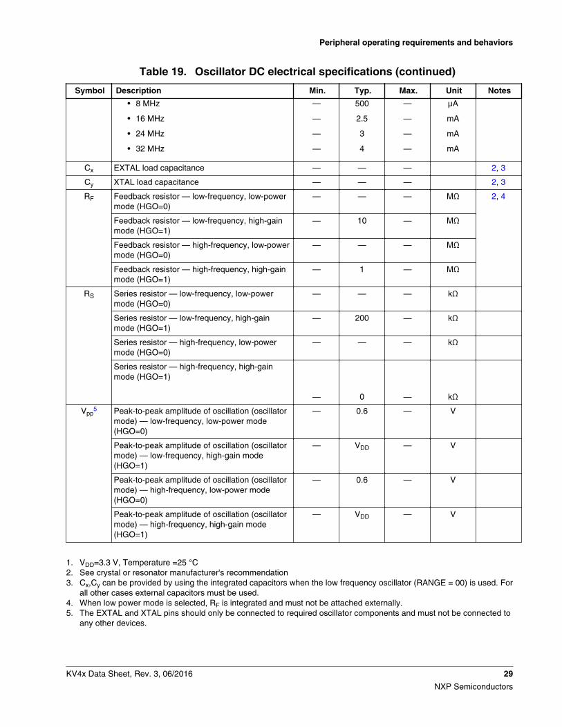
Table 19. Oscillator DC electrical specifications (continued)
Symbol Description Min. Typ. Max. Unit Notes
• 8 MHz
• 16 MHz
• 24 MHz
• 32 MHz
—
—
—
—
500
2.5
3
4
—
—
—
—
μA
mA
mA
mA
Cx EXTAL load capacitance — — — 2, 3
Cy XTAL load capacitance — — — 2, 3
RF Feedback resistor — low-frequency, low-powermode (HGO=0)
— — — MΩ 2, 4
Feedback resistor — low-frequency, high-gainmode (HGO=1)
— 10 — MΩ
Feedback resistor — high-frequency, low-powermode (HGO=0)
— — — MΩ
Feedback resistor — high-frequency, high-gainmode (HGO=1)
— 1 — MΩ
RS Series resistor — low-frequency, low-powermode (HGO=0)
— — — kΩ
Series resistor — low-frequency, high-gainmode (HGO=1)
— 200 — kΩ
Series resistor — high-frequency, low-powermode (HGO=0)
— — — kΩ
Series resistor — high-frequency, high-gainmode (HGO=1)
—
0
—
kΩ
Vpp5 Peak-to-peak amplitude of oscillation (oscillator
mode) — low-frequency, low-power mode(HGO=0)
— 0.6 — V
Peak-to-peak amplitude of oscillation (oscillatormode) — low-frequency, high-gain mode(HGO=1)
— VDD — V
Peak-to-peak amplitude of oscillation (oscillatormode) — high-frequency, low-power mode(HGO=0)
— 0.6 — V
Peak-to-peak amplitude of oscillation (oscillatormode) — high-frequency, high-gain mode(HGO=1)
— VDD — V
1. VDD=3.3 V, Temperature =25 °C2. See crystal or resonator manufacturer's recommendation3. Cx,Cy can be provided by using the integrated capacitors when the low frequency oscillator (RANGE = 00) is used. For
all other cases external capacitors must be used.4. When low power mode is selected, RF is integrated and must not be attached externally.5. The EXTAL and XTAL pins should only be connected to required oscillator components and must not be connected to
any other devices.
Peripheral operating requirements and behaviors
KV4x Data Sheet, Rev. 3, 06/2016 29
NXP Semiconductors
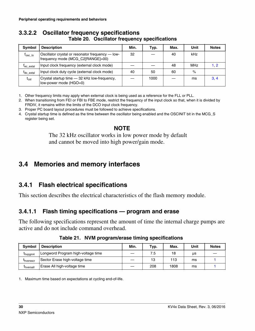
3.3.2.2 Oscillator frequency specificationsTable 20. Oscillator frequency specifications
Symbol Description Min. Typ. Max. Unit Notes
fosc_lo Oscillator crystal or resonator frequency — low-frequency mode (MCG_C2[RANGE]=00)
32 — 40 kHz
fec_extal Input clock frequency (external clock mode) — — 48 MHz 1, 2
tdc_extal Input clock duty cycle (external clock mode) 40 50 60 %
tcst Crystal startup time — 32 kHz low-frequency,low-power mode (HGO=0)
— 1000 — ms 3, 4
1. Other frequency limits may apply when external clock is being used as a reference for the FLL or PLL.2. When transitioning from FEI or FBI to FBE mode, restrict the frequency of the input clock so that, when it is divided by
FRDIV, it remains within the limits of the DCO input clock frequency.3. Proper PC board layout procedures must be followed to achieve specifications.4. Crystal startup time is defined as the time between the oscillator being enabled and the OSCINIT bit in the MCG_S
register being set.
NOTEThe 32 kHz oscillator works in low power mode by defaultand cannot be moved into high power/gain mode.
3.4 Memories and memory interfaces
3.4.1 Flash electrical specifications
This section describes the electrical characteristics of the flash memory module.
3.4.1.1 Flash timing specifications — program and erase
The following specifications represent the amount of time the internal charge pumps areactive and do not include command overhead.
Table 21. NVM program/erase timing specifications
Symbol Description Min. Typ. Max. Unit Notes
thvpgm4 Longword Program high-voltage time — 7.5 18 μs —
thversscr Sector Erase high-voltage time — 13 113 ms 1
thversall Erase All high-voltage time — 208 1808 ms 1
1. Maximum time based on expectations at cycling end-of-life.
Peripheral operating requirements and behaviors
30 KV4x Data Sheet, Rev. 3, 06/2016
NXP Semiconductors
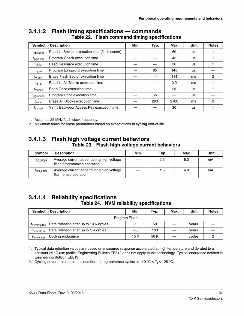
3.4.1.2 Flash timing specifications — commandsTable 22. Flash command timing specifications
Symbol Description Min. Typ. Max. Unit Notes
trd1sec4k Read 1s Section execution time (flash sector) — — 60 μs 1
tpgmchk Program Check execution time — — 45 μs 1
trdrsrc Read Resource execution time — — 30 μs 1
tpgm4 Program Longword execution time — 65 145 μs —
tersscr Erase Flash Sector execution time — 14 114 ms 2
trd1all Read 1s All Blocks execution time — — 0.9 ms 1
trdonce Read Once execution time — — 25 μs 1
tpgmonce Program Once execution time — 65 — μs —
tersall Erase All Blocks execution time — 280 2100 ms 2
tvfykey Verify Backdoor Access Key execution time — — 30 μs 1
1. Assumes 25 MHz flash clock frequency.2. Maximum times for erase parameters based on expectations at cycling end-of-life.
3.4.1.3 Flash high voltage current behaviorsTable 23. Flash high voltage current behaviors
Symbol Description Min. Typ. Max. Unit
IDD_PGM Average current adder during high voltageflash programming operation
— 2.5 6.0 mA
IDD_ERS Average current adder during high voltageflash erase operation
— 1.5 4.0 mA
3.4.1.4 Reliability specificationsTable 24. NVM reliability specifications
Symbol Description Min. Typ.1 Max. Unit Notes
Program Flash
tnvmretp10k Data retention after up to 10 K cycles 5 50 — years —
tnvmretp1k Data retention after up to 1 K cycles 20 100 — years —
nnvmcycp Cycling endurance 10 K 50 K — cycles 2
1. Typical data retention values are based on measured response accelerated at high temperature and derated to aconstant 25 °C use profile. Engineering Bulletin EB618 does not apply to this technology. Typical endurance defined inEngineering Bulletin EB619.
2. Cycling endurance represents number of program/erase cycles at –40 °C ≤ Tj ≤ 125 °C.
Peripheral operating requirements and behaviors
KV4x Data Sheet, Rev. 3, 06/2016 31
NXP Semiconductors
3.5 Security and integrity modules
There are no specifications necessary for the device's security and integrity modules.
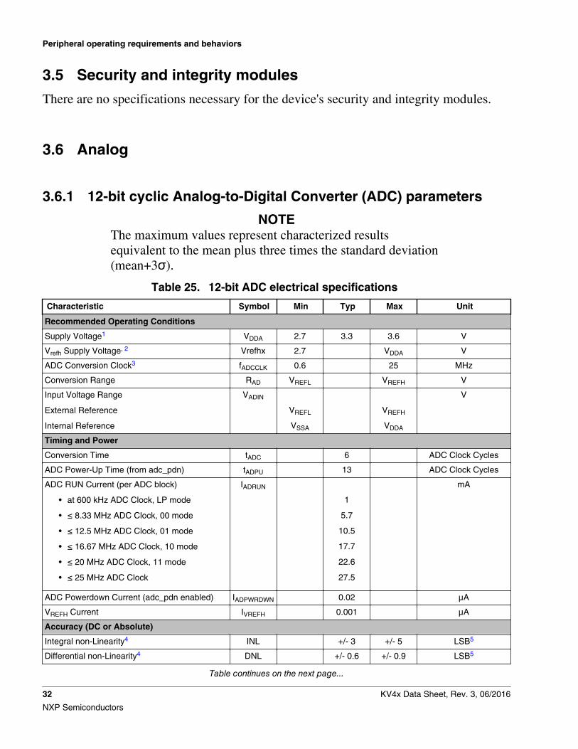
3.6 Analog
3.6.1 12-bit cyclic Analog-to-Digital Converter (ADC) parameters
NOTEThe maximum values represent characterized resultsequivalent to the mean plus three times the standard deviation(mean+3σ).
Table 25. 12-bit ADC electrical specifications
Characteristic Symbol Min Typ Max Unit
Recommended Operating Conditions
Supply Voltage1 VDDA 2.7 3.3 3.6 V
Vrefh Supply Voltage, 2 Vrefhx 2.7 VDDA V
ADC Conversion Clock3 fADCCLK 0.6 25 MHz
Conversion Range RAD VREFL VREFH V
Input Voltage Range
External Reference
Internal Reference
VADIN
VREFL
VSSA
VREFH
VDDA
V
Timing and Power
Conversion Time tADC 6 ADC Clock Cycles
ADC Power-Up Time (from adc_pdn) tADPU 13 ADC Clock Cycles
ADC RUN Current (per ADC block)
• at 600 kHz ADC Clock, LP mode
• ≤ 8.33 MHz ADC Clock, 00 mode
• ≤ 12.5 MHz ADC Clock, 01 mode
• ≤ 16.67 MHz ADC Clock, 10 mode
• ≤ 20 MHz ADC Clock, 11 mode
• ≤ 25 MHz ADC Clock
IADRUN
1
5.7
10.5
17.7
22.6
27.5
mA
ADC Powerdown Current (adc_pdn enabled) IADPWRDWN 0.02 µA
VREFH Current IVREFH 0.001 µA
Accuracy (DC or Absolute)
Integral non-Linearity4 INL +/- 3 +/- 5 LSB5
Differential non-Linearity4 DNL +/- 0.6 +/- 0.9 LSB5
Table continues on the next page...
Peripheral operating requirements and behaviors
32 KV4x Data Sheet, Rev. 3, 06/2016
NXP Semiconductors
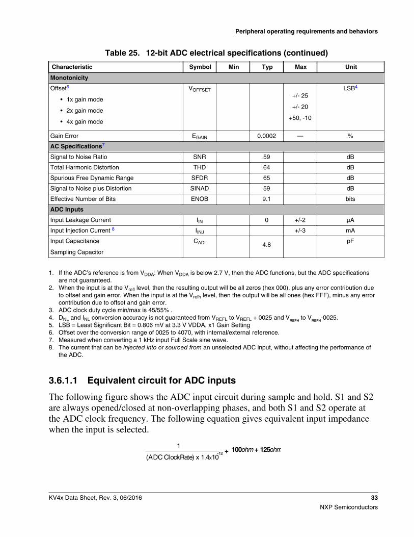
Table 25. 12-bit ADC electrical specifications (continued)
Characteristic Symbol Min Typ Max Unit
Monotonicity
Offset6
• 1x gain mode
• 2x gain mode
• 4x gain mode
VOFFSET+/- 25
+/- 20
+50, -10
LSB4
Gain Error EGAIN 0.0002 — %
AC Specifications7
Signal to Noise Ratio SNR 59 dB
Total Harmonic Distortion THD 64 dB
Spurious Free Dynamic Range SFDR 65 dB
Signal to Noise plus Distortion SINAD 59 dB
Effective Number of Bits ENOB 9.1 bits
ADC Inputs
Input Leakage Current IIN 0 +/-2 µA
Input Injection Current 8 IINJ +/-3 mA
Input Capacitance
Sampling Capacitor
CADI 4.8pF
1. If the ADC’s reference is from VDDA: When VDDA is below 2.7 V, then the ADC functions, but the ADC specificationsare not guaranteed.
2. When the input is at the Vrefl level, then the resulting output will be all zeros (hex 000), plus any error contribution dueto offset and gain error. When the input is at the Vrefh level, then the output will be all ones (hex FFF), minus any errorcontribution due to offset and gain error.
3. ADC clock duty cycle min/max is 45/55% .4. DNL and INL conversion accuracy is not guaranteed from VREFL to VREFL + 0025 and V
REFH to V
REFH-0025.
5. LSB = Least Significant Bit = 0.806 mV at 3.3 V VDDA, x1 Gain Setting6. Offset over the conversion range of 0025 to 4070, with internal/external reference.7. Measured when converting a 1 kHz input Full Scale sine wave.8. The current that can be injected into or sourced from an unselected ADC input, without affecting the performance of
the ADC.
3.6.1.1 Equivalent circuit for ADC inputs
The following figure shows the ADC input circuit during sample and hold. S1 and S2are always opened/closed at non-overlapping phases, and both S1 and S2 operate atthe ADC clock frequency. The following equation gives equivalent input impedancewhen the input is selected.
Freescale Semiconductor32
1
(ADC ClockRate) x 1.4x10⁻¹² + 100ohm+ 125ohm
Peripheral operating requirements and behaviors
KV4x Data Sheet, Rev. 3, 06/2016 33
NXP Semiconductors
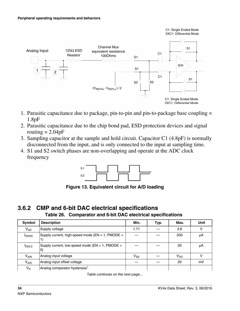
1 2
Analog Input
S1
S1
S2
C1
C1
S/H
C1: Single Ended Mode2XC1: Differential Mode
(VREFHx - VREFLx ) / 2
125 ESDResistor
S2
S1
S1
Channel Muxequivalent resistance
100Ohms
C1: Single Ended Mode2XC1: Differential Mode
1. Parasitic capacitance due to package, pin-to-pin and pin-to-package base coupling =1.8pF
2. Parasitic capacitance due to the chip bond pad, ESD protection devices and signalrouting = 2.04pF
3. Sampling capacitor at the sample and hold circuit. Capacitor C1 (4.8pF) is normallydisconnected from the input, and is only connected to the input at sampling time.
4. S1 and S2 switch phases are non-overlapping and operate at the ADC clockfrequency
S 1
S 2
Figure 13. Equivalent circuit for A/D loading
3.6.2 CMP and 6-bit DAC electrical specificationsTable 26. Comparator and 6-bit DAC electrical specifications
Symbol Description Min. Typ. Max. Unit
VDD Supply voltage 1.71 — 3.6 V
IDDHS Supply current, high-speed mode (EN = 1, PMODE =1)
— — 200 μA
IDDLS Supply current, low-speed mode (EN = 1, PMODE =0)
— — 20 μA
VAIN Analog input voltage VSS — VDD V
VAIO Analog input offset voltage — — 20 mV
VH Analog comparator hysteresis1
Table continues on the next page...
Peripheral operating requirements and behaviors
34 KV4x Data Sheet, Rev. 3, 06/2016
NXP Semiconductors
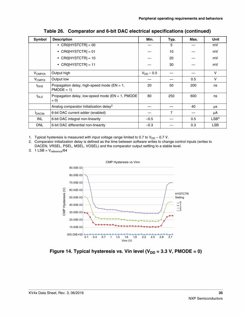
Table 26. Comparator and 6-bit DAC electrical specifications (continued)
Symbol Description Min. Typ. Max. Unit
• CR0[HYSTCTR] = 00
• CR0[HYSTCTR] = 01
• CR0[HYSTCTR] = 10
• CR0[HYSTCTR] = 11
—
—
—
—
5
10
20
30
—
—
—
—
mV
mV
mV
mV
VCMPOh Output high VDD – 0.5 — — V
VCMPOl Output low — — 0.5 V
tDHS Propagation delay, high-speed mode (EN = 1,PMODE = 1)
20 50 200 ns
tDLS Propagation delay, low-speed mode (EN = 1, PMODE= 0)
80 250 600 ns
Analog comparator initialization delay2 — — 40 μs
IDAC6b 6-bit DAC current adder (enabled) — 7 — μA
INL 6-bit DAC integral non-linearity –0.5 — 0.5 LSB3
DNL 6-bit DAC differential non-linearity –0.3 — 0.3 LSB
1. Typical hysteresis is measured with input voltage range limited to 0.7 to VDD – 0.7 V.2. Comparator initialization delay is defined as the time between software writes to change control inputs (writes to
DACEN, VRSEL, PSEL, MSEL, VOSEL) and the comparator output settling to a stable level.3. 1 LSB = Vreference/64
CMP Hysteresis vs Vinn
012
HYSTCTR Setting
000.00E+00
0.1 0.4 0.7 1 1.3 1.6 1.9 2.2 2.5 2.8 3.1
Vinn (V)
330.00E-03
20.00E-03
10.00E-03
40.00E-03
50.00E-03
60.00E-03
70.00E-03
80.00E-03
90.00E-03
CM
P H
yste
resi
s (V
)
Figure 14. Typical hysteresis vs. Vin level (VDD = 3.3 V, PMODE = 0)
Peripheral operating requirements and behaviors
KV4x Data Sheet, Rev. 3, 06/2016 35
NXP Semiconductors
180.00E-03
CMP Hysteresis vs Vinn
012
HYSTCTR Setting
60.00E-03
0.1 0.4 0.7 1 1.3 1.6 1.9 2.2 2.5 2.8 3.1
CM
P H
yste
resi
s (V
)
Vinn (V)
3
-20.00E-03
000.00E+00
20.00E-03
40.00E-03
80.00E-03
100.00E-03
120.00E-03
140.00E-03
160.00E-03
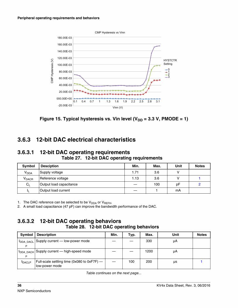
Figure 15. Typical hysteresis vs. Vin level (VDD = 3.3 V, PMODE = 1)
3.6.3 12-bit DAC electrical characteristics
3.6.3.1 12-bit DAC operating requirementsTable 27. 12-bit DAC operating requirements
Symbol Desciption Min. Max. Unit Notes
VDDA Supply voltage 1.71 3.6 V
VDACR Reference voltage 1.13 3.6 V 1
CL Output load capacitance — 100 pF 2
IL Output load current — 1 mA
1. The DAC reference can be selected to be VDDA or VREFH.2. A small load capacitance (47 pF) can improve the bandwidth performance of the DAC.
3.6.3.2 12-bit DAC operating behaviorsTable 28. 12-bit DAC operating behaviors
Symbol Description Min. Typ. Max. Unit Notes
IDDA_DACL
P
Supply current — low-power mode — — 330 μA
IDDA_DACH
P
Supply current — high-speed mode — — 1200 μA
tDACLP Full-scale settling time (0x080 to 0xF7F) —low-power mode
— 100 200 μs 1
Table continues on the next page...
Peripheral operating requirements and behaviors
36 KV4x Data Sheet, Rev. 3, 06/2016
NXP Semiconductors
Table 28. 12-bit DAC operating behaviors (continued)
Symbol Description Min. Typ. Max. Unit Notes
tDACHP Full-scale settling time (0x080 to 0xF7F) —high-power mode
— 15 30 μs 1
tCCDACLP Code-to-code settling time (0xBF8 to0xC08)
• High-speed mode• Low speed mode
—1
5μs 1
Vdacoutl DAC output voltage range low — high-speed mode, no load, DAC set to 0x000
— — 100 mV
Vdacouth DAC output voltage range high — high-speed mode, no load, DAC set to 0xFFF
VDACR−100
— VDACR mV
INL Integral non-linearity error — high speedmode
— — ±8 LSB 2
DNL Differential non-linearity error — VDACR > 2V
— — ±1 LSB 3
DNL Differential non-linearity error — VDACR =VREF_OUT
— — ±1 LSB 4
VOFFSET Offset error — ±0.4 ±0.8 %FSR 5
EG Gain error — ±0.1 ±0.6 %FSR 5
PSRR Power supply rejection ratio, VDDA ≥ 2.4 V 60 — 90 dB
TCO Temperature coefficient offset voltage — 3.7 — μV/C 6
TGE Temperature coefficient gain error — 0.000421 — %FSR/C
Rop Output resistance (load = 3 kΩ) — — 250 Ω
SR Slew rate -80h→ F7Fh→ 80h
• High power (SPHP)
• Low power (SPLP)
1.2
0.05
1.7
0.12
—
—
V/μs
BW 3dB bandwidth
• High power (SPHP)
• Low power (SPLP)
550
40
—
—
—
—
kHz
1. Settling within ±1 LSB2. The INL is measured for 0 + 100 mV to VDACR −100 mV3. The DNL is measured for 0 + 100 mV to VDACR −100 mV4. The DNL is measured for 0 + 100 mV to VDACR −100 mV with VDDA > 2.4 V5. Calculated by a best fit curve from VSS + 100 mV to VDACR − 100 mV6. VDDA = 3.0 V, reference select set for VDDA (DACx_CO:DACRFS = 1), high power mode (DACx_C0:LPEN = 0), DAC
set to 0x800, temperature range is across the full range of the device
Peripheral operating requirements and behaviors
KV4x Data Sheet, Rev. 3, 06/2016 37
NXP Semiconductors
Digital Code
DAC
12 IN
L (L
SB)
0
500 1000 1500 2000 2500 3000 3500 4000
2
4
6
8
-2
-4
-6
-80
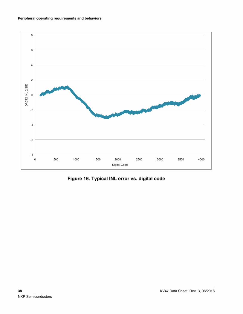
Figure 16. Typical INL error vs. digital code
Peripheral operating requirements and behaviors
38 KV4x Data Sheet, Rev. 3, 06/2016
NXP Semiconductors
Temperature °C
DAC
12 M
id L
evel
Cod
e Vo
ltage
25 55 85 105 125
1.499
-40
1.4985
1.498
1.4975
1.497
1.4965
1.496
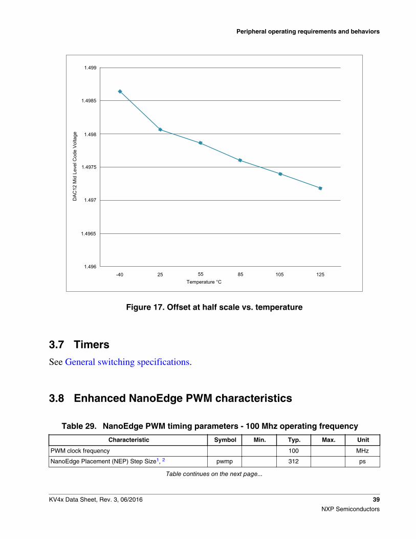
Figure 17. Offset at half scale vs. temperature
3.7 Timers
See General switching specifications.
3.8 Enhanced NanoEdge PWM characteristics
Table 29. NanoEdge PWM timing parameters - 100 Mhz operating frequency
Characteristic Symbol Min. Typ. Max. Unit
PWM clock frequency 100 MHz
NanoEdge Placement (NEP) Step Size1, 2 pwmp 312 ps
Table continues on the next page...
Peripheral operating requirements and behaviors
KV4x Data Sheet, Rev. 3, 06/2016 39
NXP Semiconductors
Table 29. NanoEdge PWM timing parameters - 100 Mhz operating frequency (continued)
Characteristic Symbol Min. Typ. Max. Unit
Delay for fault input activating to PWM outputdeactivated
1 ns
Power-up Time3 tpu 25 μs
1. Reference 100 MHz in NanoEdge Placement mode.2. Temperature and voltage variations do not affect NanoEdge Placement step size.3. Powerdown to NanoEdge mode transition.
Table 30. NanoEdge PWM timing parameters - 84 Mhz operating frequency
Characteristic Symbol Min. Typ. Max. Unit
PWM clock frequency 84 MHz
NanoEdge Placement (NEP) Step Size1, 2 pwmp 372 ps
Delay for fault input activating to PWM output deactivated 1 ns
Power-up Time3 tpu 30 μs
1. Reference 84 MHz in NanoEdge Placement mode.2. Temperature and voltage variations do not affect NanoEdge Placement step size.3. Powerdown to NanoEdge mode transition.
3.9 Communication interfaces
3.9.1 SPI (DSPI) switching specifications (limited voltage range)
The DMA Serial Peripheral Interface (DSPI) provides a synchronous serial bus withmaster and slave operations. Many of the transfer attributes are programmable. Thetables below provide DSPI timing characteristics for classic SPI timing modes. Refer tothe DSPI chapter of the Reference Manual for information on the modified transferformats used for communicating with slower peripheral devices.
NOTEFast pads:
• SIN: PTE19• SOUT: PTE18• SCK: PTE17• PCS: PTE16
Open drain pads:
Peripheral operating requirements and behaviors
40 KV4x Data Sheet, Rev. 3, 06/2016
NXP Semiconductors
• SIN: PTC7• SOUT: PTC6
Table 31. Master mode DSPI timing for normal pads (limited voltage range)
Num Description Min. Max. Unit Notes
Operating voltage 2.7 3.6 V
Frequency of operation — 25 MHz
DS1 DSPI_SCK output cycle time 2 x tBUS — ns
DS2 DSPI_SCK output high/low time (tSCK/2) − 2 (tSCK/2) + 2 ns
DS3 DSPI_PCSn to DSPI_SCK output valid (tBUS x 2) −2
— ns 1
DS4 DSPI_SCK to DSPI_PCSn output hold (tBUS x 2) −2
— ns 2
DS5 DSPI_SCK to DSPI_SOUT valid — 8.5 ns
DS6 DSPI_SCK to DSPI_SOUT invalid −2 — ns
DS7 DSPI_SIN to DSPI_SCK input setup 17 — ns
DS8 DSPI_SCK to DSPI_SIN input hold 0 — ns
1. The delay is programmable in SPIx_CTARn[PSSCK] and SPIx_CTARn[CSSCK].2. The delay is programmable in SPIx_CTARn[PASC] and SPIx_CTARn[ASC].
Table 32. Master mode DSPI timing for fast pads (limited voltage range)
Num Description Min. Max. Unit Notes
Operating voltage 2.7 3.6 V
Frequency of operation — 37.5 MHz
DS1 DSPI_SCK output cycle time 2 x tBUS — ns
DS2 DSPI_SCK output high/low time (tSCK/2) − 2 (tSCK/2) + 2 ns
DS3 DSPI_PCSn to DSPI_SCK output valid (tBUS x 2) −2
— ns 1
DS4 DSPI_SCK to DSPI_PCSn output hold (tBUS x 2) −2
— ns 2
DS5 DSPI_SCK to DSPI_SOUT valid — 8.5 ns
DS6 DSPI_SCK to DSPI_SOUT invalid −2 — ns
DS7 DSPI_SIN to DSPI_SCK input setup 13 — ns
DS8 DSPI_SCK to DSPI_SIN input hold 0 — ns
1. The delay is programmable in SPIx_CTARn[PSSCK] and SPIx_CTARn[CSSCK].2. The delay is programmable in SPIx_CTARn[PASC] and SPIx_CTARn[ASC].
Table 33. Master mode DSPI timing for open drain pads (limited voltage range)
Num Description Min. Max. Unit Notes
Operating voltage 2.7 3.6 V
Table continues on the next page...
Peripheral operating requirements and behaviors
KV4x Data Sheet, Rev. 3, 06/2016 41
NXP Semiconductors
Table 33. Master mode DSPI timing for open drain pads (limited voltage range) (continued)
Num Description Min. Max. Unit Notes
Frequency of operation — 25 MHz
DS1 DSPI_SCK output cycle time 2 x tBUS — ns
DS2 DSPI_SCK output high/low time (tSCK/2) − 2 (tSCK/2) + 2 ns
DS3 DSPI_PCSn to DSPI_SCK output valid (tBUS x 2) −2
— ns 1
DS4 DSPI_SCK to DSPI_PCSn output hold (tBUS x 2) −2
— ns 2
DS5 DSPI_SCK to DSPI_SOUT valid — 15.5 ns
DS6 DSPI_SCK to DSPI_SOUT invalid −3 — ns
DS7 DSPI_SIN to DSPI_SCK input setup 17 — ns
DS8 DSPI_SCK to DSPI_SIN input hold 0 — ns
1. The delay is programmable in SPIx_CTARn[PSSCK] and SPIx_CTARn[CSSCK].2. The delay is programmable in SPIx_CTARn[PASC] and SPIx_CTARn[ASC].
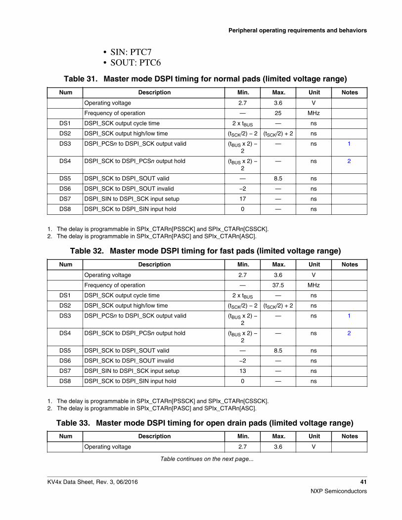
DS3 DS4DS1DS2
DS7DS8
First data Last dataDS5
First data Data Last data
DS6
Data
DSPI_PCSn
DSPI_SCK
(CPOL=0)
DSPI_SIN
DSPI_SOUT
Figure 18. DSPI classic SPI timing — master mode
Table 34. Slave mode DSPI timing for normal pads (limited voltage range)
Num Description Min. Max. Unit
Operating voltage 2.7 3.6 V
Frequency of operation 12.5 MHz
DS9 DSPI_SCK input cycle time 4 x tBUS — ns
DS10 DSPI_SCK input high/low time (tSCK/2) − 2 (tSCK/2) + 2 ns
DS11 DSPI_SCK to DSPI_SOUT valid — 21 ns
DS12 DSPI_SCK to DSPI_SOUT invalid 0 — ns
DS13 DSPI_SIN to DSPI_SCK input setup 2 — ns
DS14 DSPI_SCK to DSPI_SIN input hold 7 — ns
DS15 DSPI_SS active to DSPI_SOUT driven — 15 ns
DS16 DSPI_SS inactive to DSPI_SOUT not driven — 15 ns
Peripheral operating requirements and behaviors
42 KV4x Data Sheet, Rev. 3, 06/2016
NXP Semiconductors
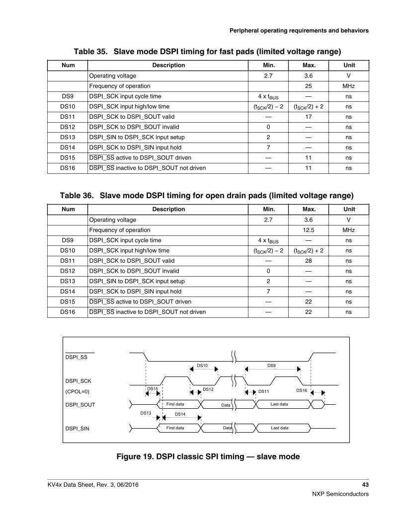
Table 35. Slave mode DSPI timing for fast pads (limited voltage range)
Num Description Min. Max. Unit
Operating voltage 2.7 3.6 V
Frequency of operation 25 MHz
DS9 DSPI_SCK input cycle time 4 x tBUS — ns
DS10 DSPI_SCK input high/low time (tSCK/2) − 2 (tSCK/2) + 2 ns
DS11 DSPI_SCK to DSPI_SOUT valid — 17 ns
DS12 DSPI_SCK to DSPI_SOUT invalid 0 — ns
DS13 DSPI_SIN to DSPI_SCK input setup 2 — ns
DS14 DSPI_SCK to DSPI_SIN input hold 7 — ns
DS15 DSPI_SS active to DSPI_SOUT driven — 11 ns
DS16 DSPI_SS inactive to DSPI_SOUT not driven — 11 ns
Table 36. Slave mode DSPI timing for open drain pads (limited voltage range)
Num Description Min. Max. Unit
Operating voltage 2.7 3.6 V
Frequency of operation 12.5 MHz
DS9 DSPI_SCK input cycle time 4 x tBUS — ns
DS10 DSPI_SCK input high/low time (tSCK/2) − 2 (tSCK/2) + 2 ns
DS11 DSPI_SCK to DSPI_SOUT valid — 28 ns
DS12 DSPI_SCK to DSPI_SOUT invalid 0 — ns
DS13 DSPI_SIN to DSPI_SCK input setup 2 — ns
DS14 DSPI_SCK to DSPI_SIN input hold 7 — ns
DS15 DSPI_SS active to DSPI_SOUT driven — 22 ns
DS16 DSPI_SS inactive to DSPI_SOUT not driven — 22 ns
First data Last data
First data Data Last data
Data
DS15
DS10 DS9
DS16DS11DS12
DS14DS13
DSPI_SS
DSPI_SCK
(CPOL=0)
DSPI_SOUT
DSPI_SIN
Figure 19. DSPI classic SPI timing — slave mode
Peripheral operating requirements and behaviors
KV4x Data Sheet, Rev. 3, 06/2016 43
NXP Semiconductors
3.9.2 SPI (DSPI) switching specifications (full voltage range)
The DMA Serial Peripheral Interface (DSPI) provides a synchronous serial bus withmaster and slave operations. Many of the transfer attributes are programmable. Thetables below provides DSPI timing characteristics for classic SPI timing modes. Referto the DSPI chapter of the Reference Manual for information on the modified transferformats used for communicating with slower peripheral devices.
NOTEFast pads:
• SIN: PTE19• SOUT: PTE18• SCK: PTE17• PCS: PTE16
Open drain pads:• SIN: PTC7• SOUT: PTC6
Table 37. Master mode DSPI timing for normal pads (full voltage range)
Num Description Min. Max. Unit Notes
Operating voltage 1.71 3.6 V 1
Frequency of operation — 18.75 MHz
DS1 DSPI_SCK output cycle time 4 x tBUS — ns
DS2 DSPI_SCK output high/low time (tSCK/2) - 4 (tSCK/2) + 4 ns
DS3 DSPI_PCSn valid to DSPI_SCK delay (tBUS x 2) −4
— ns 2
DS4 DSPI_SCK to DSPI_PCSn invalid delay (tBUS x 2) −4
— ns 3
DS5 DSPI_SCK to DSPI_SOUT valid — 10 ns
DS6 DSPI_SCK to DSPI_SOUT invalid -7.8 — ns
DS7 DSPI_SIN to DSPI_SCK input setup 24 — ns
DS8 DSPI_SCK to DSPI_SIN input hold 0 — ns
1. The DSPI module can operate across the entire operating voltage for the processor, but to run across the full voltagerange the maximum frequency of operation is reduced.
2. The delay is programmable in SPIx_CTARn[PSSCK] and SPIx_CTARn[CSSCK].3. The delay is programmable in SPIx_CTARn[PASC] and SPIx_CTARn[ASC].
Peripheral operating requirements and behaviors
44 KV4x Data Sheet, Rev. 3, 06/2016
NXP Semiconductors
Table 38. Master mode DSPI timing fast pads (full voltage range)
Num Description Min. Max. Unit Notes
Operating voltage 1.71 3.6 V 1
Frequency of operation — 25 MHz
DS1 DSPI_SCK output cycle time 4 x tBUS — ns
DS2 DSPI_SCK output high/low time (tSCK/2) - 4 (tSCK/2) + 4 ns
DS3 DSPI_PCSn valid to DSPI_SCK delay (tBUS x 2) −4
— ns 2
DS4 DSPI_SCK to DSPI_PCSn invalid delay (tBUS x 2) −4
— ns 3
DS5 DSPI_SCK to DSPI_SOUT valid — 10 ns
DS6 DSPI_SCK to DSPI_SOUT invalid -7.8 — ns
DS7 DSPI_SIN to DSPI_SCK input setup 17 — ns
DS8 DSPI_SCK to DSPI_SIN input hold 0 — ns
1. The DSPI module can operate across the entire operating voltage for the processor, but to run across the full voltagerange the maximum frequency of operation is reduced.
2. The delay is programmable in SPIx_CTARn[PSSCK] and SPIx_CTARn[CSSCK].3. The delay is programmable in SPIx_CTARn[PASC] and SPIx_CTARn[ASC].
Table 39. Master mode DSPI timing open drain pads (full voltage range)
Num Description Min. Max. Unit Notes
Operating voltage 1.71 3.6 V 1
Frequency of operation — 18.75 MHz
DS1 DSPI_SCK output cycle time 4 x tBUS — ns
DS2 DSPI_SCK output high/low time (tSCK/2) - 4 (tSCK/2) + 4 ns
DS3 DSPI_PCSn valid to DSPI_SCK delay (tBUS x 2) −4
— ns 2
DS4 DSPI_SCK to DSPI_PCSn invalid delay (tBUS x 2) −4
— ns 3
DS5 DSPI_SCK to DSPI_SOUT valid — 26 ns
DS6 DSPI_SCK to DSPI_SOUT invalid -7.8 — ns
DS7 DSPI_SIN to DSPI_SCK input setup 24 — ns
DS8 DSPI_SCK to DSPI_SIN input hold 0 — ns
1. The DSPI module can operate across the entire operating voltage for the processor, but to run across the full voltagerange the maximum frequency of operation is reduced.
2. The delay is programmable in SPIx_CTARn[PSSCK] and SPIx_CTARn[CSSCK].3. The delay is programmable in SPIx_CTARn[PASC] and SPIx_CTARn[ASC].
Peripheral operating requirements and behaviors
KV4x Data Sheet, Rev. 3, 06/2016 45
NXP Semiconductors
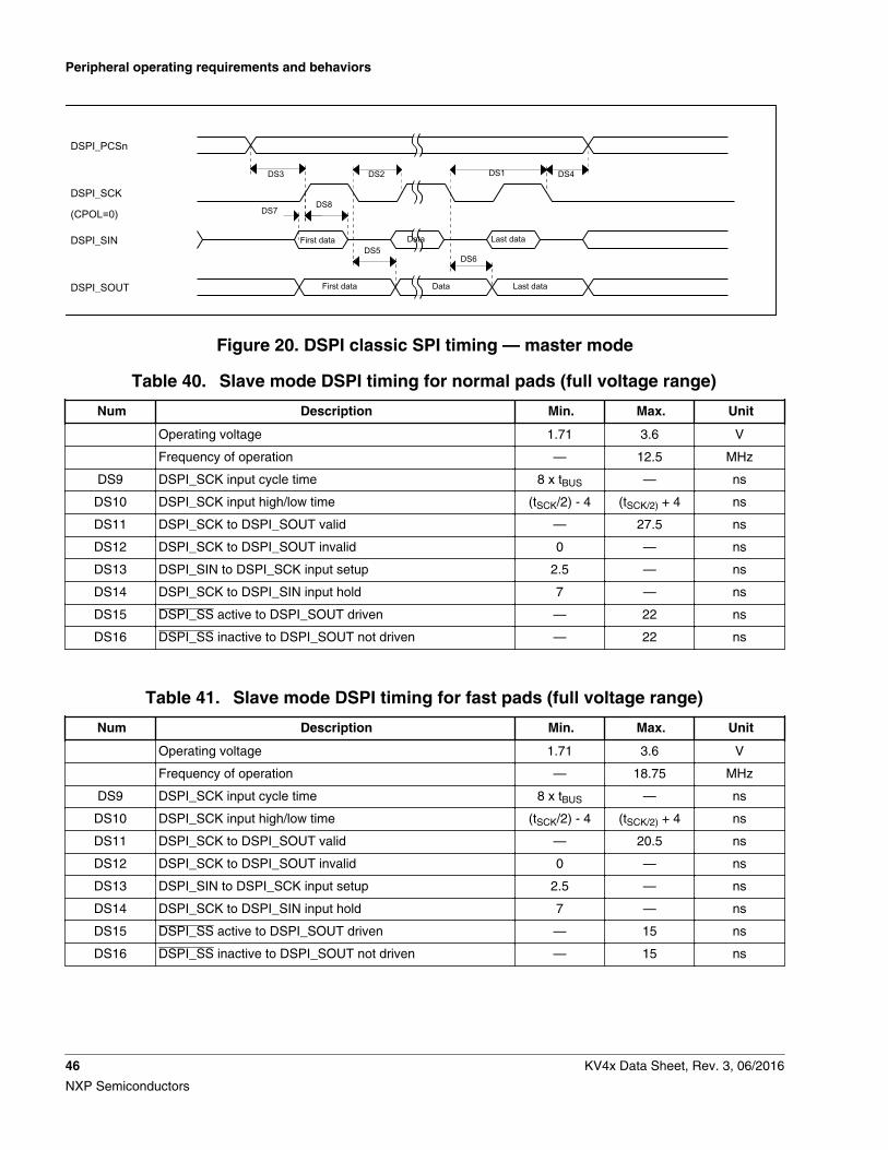
DS3 DS4DS1DS2
DS7DS8
First data Last dataDS5
First data Data Last data
DS6
Data
DSPI_PCSn
DSPI_SCK
(CPOL=0)
DSPI_SIN
DSPI_SOUT
Figure 20. DSPI classic SPI timing — master mode
Table 40. Slave mode DSPI timing for normal pads (full voltage range)
Num Description Min. Max. Unit
Operating voltage 1.71 3.6 V
Frequency of operation — 12.5 MHz
DS9 DSPI_SCK input cycle time 8 x tBUS — ns
DS10 DSPI_SCK input high/low time (tSCK/2) - 4 (tSCK/2) + 4 ns
DS11 DSPI_SCK to DSPI_SOUT valid — 27.5 ns
DS12 DSPI_SCK to DSPI_SOUT invalid 0 — ns
DS13 DSPI_SIN to DSPI_SCK input setup 2.5 — ns
DS14 DSPI_SCK to DSPI_SIN input hold 7 — ns
DS15 DSPI_SS active to DSPI_SOUT driven — 22 ns
DS16 DSPI_SS inactive to DSPI_SOUT not driven — 22 ns
Table 41. Slave mode DSPI timing for fast pads (full voltage range)
Num Description Min. Max. Unit
Operating voltage 1.71 3.6 V
Frequency of operation — 18.75 MHz
DS9 DSPI_SCK input cycle time 8 x tBUS — ns
DS10 DSPI_SCK input high/low time (tSCK/2) - 4 (tSCK/2) + 4 ns
DS11 DSPI_SCK to DSPI_SOUT valid — 20.5 ns
DS12 DSPI_SCK to DSPI_SOUT invalid 0 — ns
DS13 DSPI_SIN to DSPI_SCK input setup 2.5 — ns
DS14 DSPI_SCK to DSPI_SIN input hold 7 — ns
DS15 DSPI_SS active to DSPI_SOUT driven — 15 ns
DS16 DSPI_SS inactive to DSPI_SOUT not driven — 15 ns
Peripheral operating requirements and behaviors
46 KV4x Data Sheet, Rev. 3, 06/2016
NXP Semiconductors
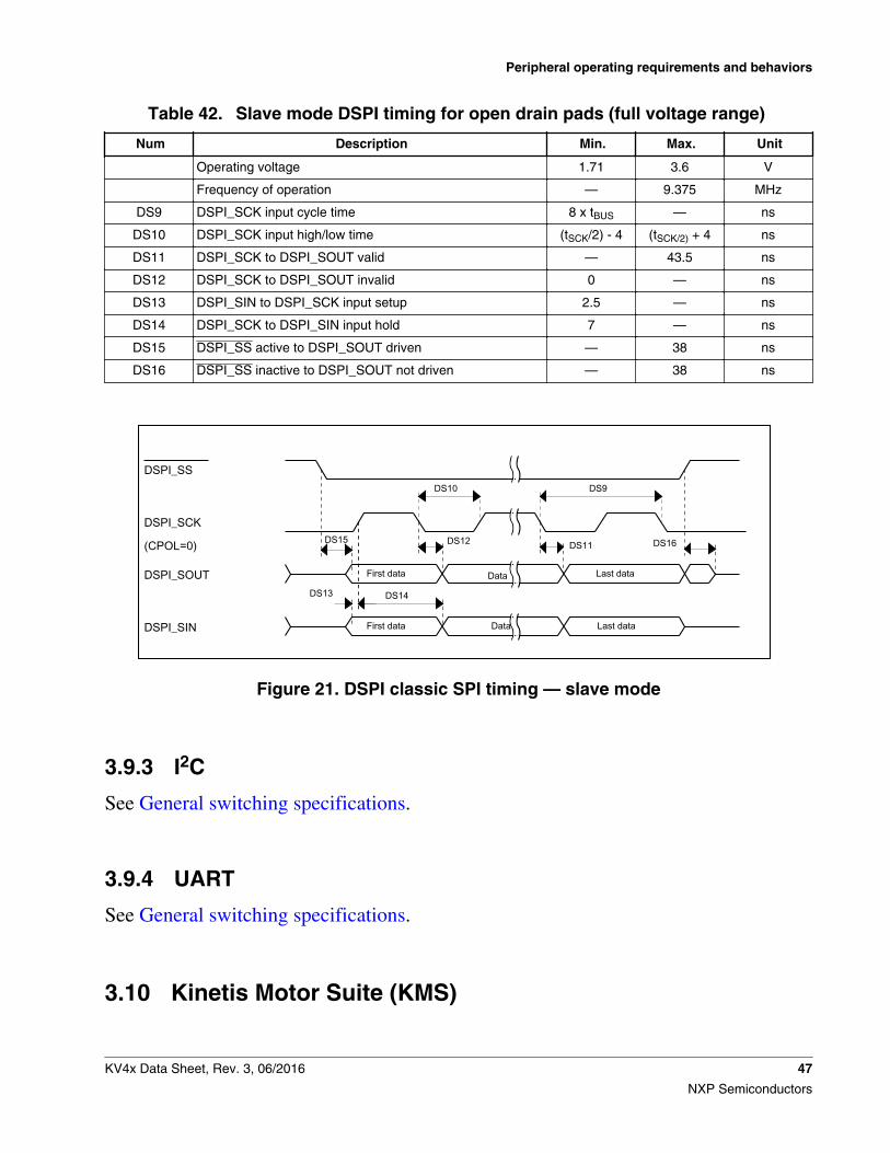
Table 42. Slave mode DSPI timing for open drain pads (full voltage range)
Num Description Min. Max. Unit
Operating voltage 1.71 3.6 V
Frequency of operation — 9.375 MHz
DS9 DSPI_SCK input cycle time 8 x tBUS — ns
DS10 DSPI_SCK input high/low time (tSCK/2) - 4 (tSCK/2) + 4 ns
DS11 DSPI_SCK to DSPI_SOUT valid — 43.5 ns
DS12 DSPI_SCK to DSPI_SOUT invalid 0 — ns
DS13 DSPI_SIN to DSPI_SCK input setup 2.5 — ns
DS14 DSPI_SCK to DSPI_SIN input hold 7 — ns
DS15 DSPI_SS active to DSPI_SOUT driven — 38 ns
DS16 DSPI_SS inactive to DSPI_SOUT not driven — 38 ns
First data Last data
First data Data Last data
Data
DS15
DS10 DS9
DS16DS11DS12
DS14DS13
DSPI_SS
DSPI_SCK
(CPOL=0)
DSPI_SOUT
DSPI_SIN
Figure 21. DSPI classic SPI timing — slave mode
3.9.3 I2C
See General switching specifications.
3.9.4 UART
See General switching specifications.
3.10 Kinetis Motor Suite (KMS)
Peripheral operating requirements and behaviors
KV4x Data Sheet, Rev. 3, 06/2016 47
NXP Semiconductors
Kinetis Motor Suite is a bundled software solution that enables the rapid configurationof motor drive systems, and accelerates development of the final motor driveapplication.
Several members of the KV4x family are enabled with Kinetis Motor Suite. Theenabled devices can be identified within the orderable part numbers in KMS Orderablepart numbers summary . For more information,see Kinetis Motor Suite User's Guide(KMS100UG) and Kinetis Motor Suite API Reference Manual (KMS100RM).
NOTETo find the associated resource, go to http://www.nxp.comand perform a search using the Document ID.
4 Dimensions
4.1 Obtaining package dimensions
Package dimensions are provided in package drawings.
To find a package drawing, go to www.nxp.com and perform a keyword search for thedrawing’s document number:
If you want the drawing for this package Then use this document number
48-pin LQFP 98ASH00962A
64-pin LQFP 98ASS23234W
100-pin LQFP 98ASS23308W
5 Pinout
5.1 KV4x Signal Multiplexing and Pin Assignments
The following table shows the signals available on each pin and the locations of thesepins on the devices supported by this document. The Port Control Module is responsiblefor selecting which ALT functionality is available on each pin.
Dimensions
48 KV4x Data Sheet, Rev. 3, 06/2016
NXP Semiconductors
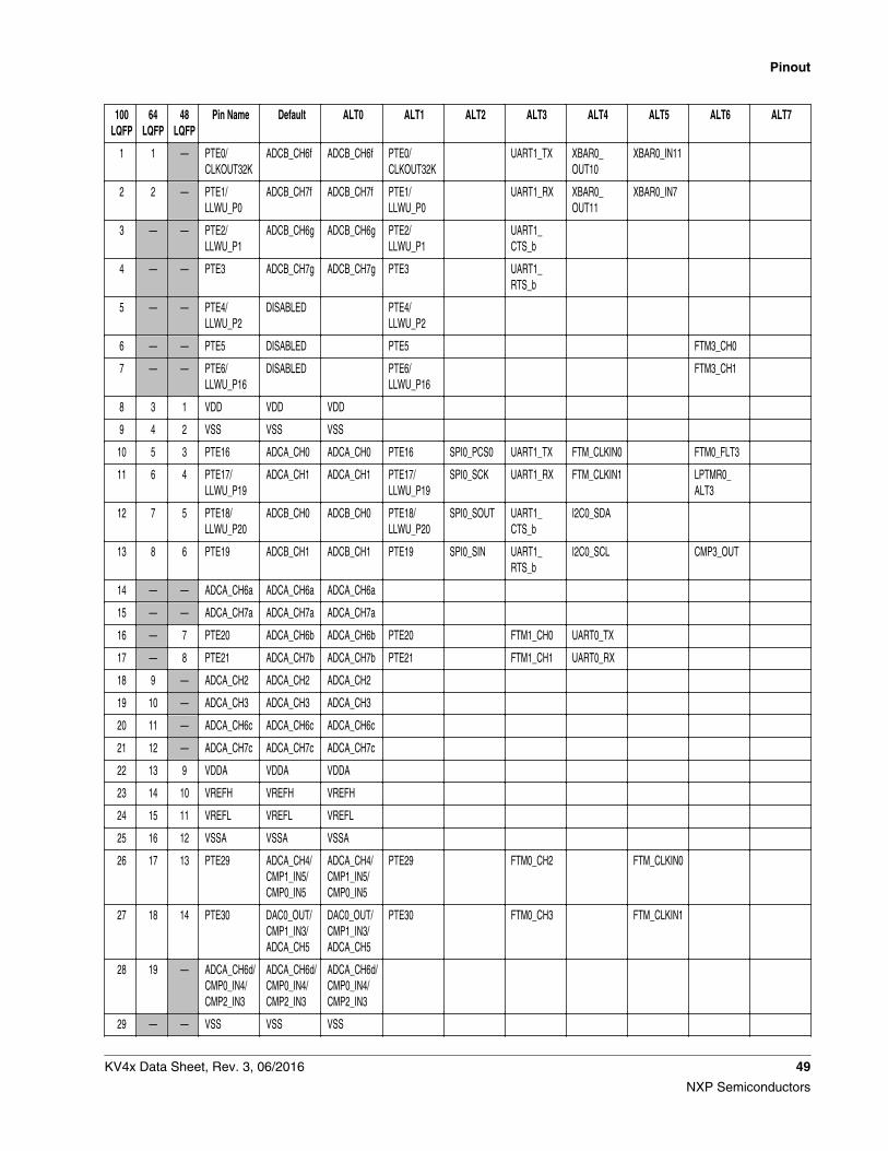
100LQFP
64LQFP
48LQFP
Pin Name Default ALT0 ALT1 ALT2 ALT3 ALT4 ALT5 ALT6 ALT7
1 1 — PTE0/CLKOUT32K
ADCB_CH6f ADCB_CH6f PTE0/CLKOUT32K
UART1_TX XBAR0_OUT10
XBAR0_IN11
2 2 — PTE1/LLWU_P0
ADCB_CH7f ADCB_CH7f PTE1/LLWU_P0
UART1_RX XBAR0_OUT11
XBAR0_IN7
3 — — PTE2/LLWU_P1
ADCB_CH6g ADCB_CH6g PTE2/LLWU_P1
UART1_CTS_b
4 — — PTE3 ADCB_CH7g ADCB_CH7g PTE3 UART1_RTS_b
5 — — PTE4/LLWU_P2
DISABLED PTE4/LLWU_P2
6 — — PTE5 DISABLED PTE5 FTM3_CH0
7 — — PTE6/LLWU_P16
DISABLED PTE6/LLWU_P16
FTM3_CH1
8 3 1 VDD VDD VDD
9 4 2 VSS VSS VSS
10 5 3 PTE16 ADCA_CH0 ADCA_CH0 PTE16 SPI0_PCS0 UART1_TX FTM_CLKIN0 FTM0_FLT3
11 6 4 PTE17/LLWU_P19
ADCA_CH1 ADCA_CH1 PTE17/LLWU_P19
SPI0_SCK UART1_RX FTM_CLKIN1 LPTMR0_ALT3
12 7 5 PTE18/LLWU_P20
ADCB_CH0 ADCB_CH0 PTE18/LLWU_P20
SPI0_SOUT UART1_CTS_b
I2C0_SDA
13 8 6 PTE19 ADCB_CH1 ADCB_CH1 PTE19 SPI0_SIN UART1_RTS_b
I2C0_SCL CMP3_OUT
14 — — ADCA_CH6a ADCA_CH6a ADCA_CH6a
15 — — ADCA_CH7a ADCA_CH7a ADCA_CH7a
16 — 7 PTE20 ADCA_CH6b ADCA_CH6b PTE20 FTM1_CH0 UART0_TX
17 — 8 PTE21 ADCA_CH7b ADCA_CH7b PTE21 FTM1_CH1 UART0_RX
18 9 — ADCA_CH2 ADCA_CH2 ADCA_CH2
19 10 — ADCA_CH3 ADCA_CH3 ADCA_CH3
20 11 — ADCA_CH6c ADCA_CH6c ADCA_CH6c
21 12 — ADCA_CH7c ADCA_CH7c ADCA_CH7c
22 13 9 VDDA VDDA VDDA
23 14 10 VREFH VREFH VREFH
24 15 11 VREFL VREFL VREFL
25 16 12 VSSA VSSA VSSA
26 17 13 PTE29 ADCA_CH4/CMP1_IN5/CMP0_IN5
ADCA_CH4/CMP1_IN5/CMP0_IN5
PTE29 FTM0_CH2 FTM_CLKIN0
27 18 14 PTE30 DAC0_OUT/CMP1_IN3/ADCA_CH5
DAC0_OUT/CMP1_IN3/ADCA_CH5
PTE30 FTM0_CH3 FTM_CLKIN1
28 19 — ADCA_CH6d/CMP0_IN4/CMP2_IN3
ADCA_CH6d/CMP0_IN4/CMP2_IN3
ADCA_CH6d/CMP0_IN4/CMP2_IN3
29 — — VSS VSS VSS
Pinout
KV4x Data Sheet, Rev. 3, 06/2016 49
NXP Semiconductors
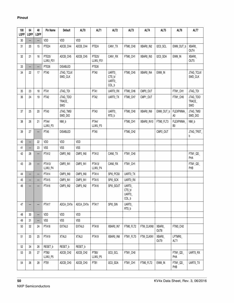
100LQFP
64LQFP
48LQFP
Pin Name Default ALT0 ALT1 ALT2 ALT3 ALT4 ALT5 ALT6 ALT7
30 — — VDD VDD VDD
31 20 15 PTE24 ADCB_CH4 ADCB_CH4 PTE24 CAN1_TX FTM0_CH0 XBAR0_IN2 I2C0_SCL EWM_OUT_b XBAR0_OUT4
32 21 16 PTE25/LLWU_P21
ADCB_CH5 ADCB_CH5 PTE25/LLWU_P21
CAN1_RX FTM0_CH1 XBAR0_IN3 I2C0_SDA EWM_IN XBAR0_OUT5
33 — — PTE26 DISABLED PTE26
34 22 17 PTA0 JTAG_TCLK/SWD_CLK
PTA0 UART0_CTS_b/UART0_COL_b
FTM0_CH5 XBAR0_IN4 EWM_IN JTAG_TCLK/SWD_CLK
35 23 18 PTA1 JTAG_TDI PTA1 UART0_RX FTM0_CH6 CMP0_OUT FTM1_CH1 JTAG_TDI
36 24 19 PTA2 JTAG_TDO/TRACE_SWO
PTA2 UART0_TX FTM0_CH7 CMP1_OUT FTM1_CH0 JTAG_TDO/TRACE_SWO
37 25 20 PTA3 JTAG_TMS/SWD_DIO
PTA3 UART0_RTS_b
FTM0_CH0 XBAR0_IN9 EWM_OUT_b FLEXPWMA_A0
JTAG_TMS/SWD_DIO
38 26 21 PTA4/LLWU_P3
NMI_b PTA4/LLWU_P3
FTM0_CH1 XBAR0_IN10 FTM0_FLT3 FLEXPWMA_B0
NMI_b
39 27 — PTA5 DISABLED PTA5 FTM0_CH2 CMP2_OUT JTAG_TRST_b
40 — 22 VDD VDD VDD
41 — 23 VSS VSS VSS
42 28 — PTA12 CMP2_IN0 CMP2_IN0 PTA12 CAN0_TX FTM1_CH0 FTM1_QD_PHA
43 29 — PTA13/LLWU_P4
CMP2_IN1 CMP2_IN1 PTA13/LLWU_P4
CAN0_RX FTM1_CH1 FTM1_QD_PHB
44 — — PTA14 CMP3_IN0 CMP3_IN0 PTA14 SPI0_PCS0 UART0_TX
45 — — PTA15 CMP3_IN1 CMP3_IN1 PTA15 SPI0_SCK UART0_RX
46 — — PTA16 CMP3_IN2 CMP3_IN2 PTA16 SPI0_SOUT UART0_CTS_b/UART0_COL_b
47 — — PTA17 ADCA_CH7e ADCA_CH7e PTA17 SPI0_SIN UART0_RTS_b
48 30 — VDD VDD VDD
49 31 — VSS VSS VSS
50 32 24 PTA18 EXTAL0 EXTAL0 PTA18 XBAR0_IN7 FTM0_FLT2 FTM_CLKIN0 XBAR0_OUT8
FTM3_CH2
51 33 25 PTA19 XTAL0 XTAL0 PTA19 XBAR0_IN8 FTM1_FLT0 FTM_CLKIN1 XBAR0_OUT9
LPTMR0_ALT1
52 34 26 RESET_b RESET_b RESET_b
53 35 27 PTB0/LLWU_P5
ADCB_CH2 ADCB_CH2 PTB0/LLWU_P5
I2C0_SCL FTM1_CH0 FTM1_QD_PHA
UART0_RX
54 36 28 PTB1 ADCB_CH3 ADCB_CH3 PTB1 I2C0_SDA FTM1_CH1 FTM0_FLT2 EWM_IN FTM1_QD_PHB
UART0_TX
Pinout
50 KV4x Data Sheet, Rev. 3, 06/2016
NXP Semiconductors
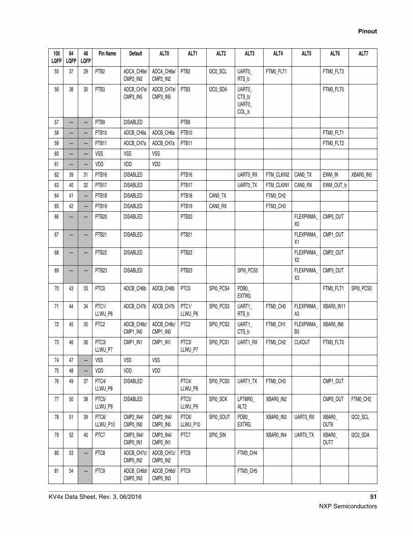
100LQFP
64LQFP
48LQFP
Pin Name Default ALT0 ALT1 ALT2 ALT3 ALT4 ALT5 ALT6 ALT7
55 37 29 PTB2 ADCA_CH6e/CMP2_IN2
ADCA_CH6e/CMP2_IN2
PTB2 I2C0_SCL UART0_RTS_b
FTM0_FLT1 FTM0_FLT3
56 38 30 PTB3 ADCB_CH7e/CMP3_IN5
ADCB_CH7e/CMP3_IN5
PTB3 I2C0_SDA UART0_CTS_b/UART0_COL_b
FTM0_FLT0
57 — — PTB9 DISABLED PTB9
58 — — PTB10 ADCB_CH6a ADCB_CH6a PTB10 FTM0_FLT1
59 — — PTB11 ADCB_CH7a ADCB_CH7a PTB11 FTM0_FLT2
60 — — VSS VSS VSS
61 — — VDD VDD VDD
62 39 31 PTB16 DISABLED PTB16 UART0_RX FTM_CLKIN2 CAN0_TX EWM_IN XBAR0_IN5
63 40 32 PTB17 DISABLED PTB17 UART0_TX FTM_CLKIN1 CAN0_RX EWM_OUT_b
64 41 — PTB18 DISABLED PTB18 CAN0_TX FTM3_CH2
65 42 — PTB19 DISABLED PTB19 CAN0_RX FTM3_CH3
66 — — PTB20 DISABLED PTB20 FLEXPWMA_X0
CMP0_OUT
67 — — PTB21 DISABLED PTB21 FLEXPWMA_X1
CMP1_OUT
68 — — PTB22 DISABLED PTB22 FLEXPWMA_X2
CMP2_OUT
69 — — PTB23 DISABLED PTB23 SPI0_PCS5 FLEXPWMA_X3
CMP3_OUT
70 43 33 PTC0 ADCB_CH6b ADCB_CH6b PTC0 SPI0_PCS4 PDB0_EXTRG
FTM0_FLT1 SPI0_PCS0
71 44 34 PTC1/LLWU_P6
ADCB_CH7b ADCB_CH7b PTC1/LLWU_P6
SPI0_PCS3 UART1_RTS_b
FTM0_CH0 FLEXPWMA_A3
XBAR0_IN11
72 45 35 PTC2 ADCB_CH6c/CMP1_IN0
ADCB_CH6c/CMP1_IN0
PTC2 SPI0_PCS2 UART1_CTS_b
FTM0_CH1 FLEXPWMA_B3
XBAR0_IN6
73 46 36 PTC3/LLWU_P7
CMP1_IN1 CMP1_IN1 PTC3/LLWU_P7
SPI0_PCS1 UART1_RX FTM0_CH2 CLKOUT FTM3_FLT0
74 47 — VSS VSS VSS
75 48 — VDD VDD VDD
76 49 37 PTC4/LLWU_P8
DISABLED PTC4/LLWU_P8
SPI0_PCS0 UART1_TX FTM0_CH3 CMP1_OUT
77 50 38 PTC5/LLWU_P9
DISABLED PTC5/LLWU_P9
SPI0_SCK LPTMR0_ALT2
XBAR0_IN2 CMP0_OUT FTM0_CH2
78 51 39 PTC6/LLWU_P10
CMP2_IN4/CMP0_IN0
CMP2_IN4/CMP0_IN0
PTC6/LLWU_P10
SPI0_SOUT PDB0_EXTRG
XBAR0_IN3 UART0_RX XBAR0_OUT6
I2C0_SCL
79 52 40 PTC7 CMP3_IN4/CMP0_IN1
CMP3_IN4/CMP0_IN1
PTC7 SPI0_SIN XBAR0_IN4 UART0_TX XBAR0_OUT7
I2C0_SDA
80 53 — PTC8 ADCB_CH7c/CMP0_IN2
ADCB_CH7c/CMP0_IN2
PTC8 FTM3_CH4
81 54 — PTC9 ADCB_CH6d/CMP0_IN3
ADCB_CH6d/CMP0_IN3
PTC9 FTM3_CH5
Pinout
KV4x Data Sheet, Rev. 3, 06/2016 51
NXP Semiconductors
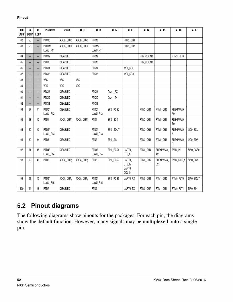
100LQFP
64LQFP
48LQFP
Pin Name Default ALT0 ALT1 ALT2 ALT3 ALT4 ALT5 ALT6 ALT7
82 55 — PTC10 ADCB_CH7d ADCB_CH7d PTC10 FTM3_CH6
83 56 — PTC11/LLWU_P11
ADCB_CH6e ADCB_CH6e PTC11/LLWU_P11
FTM3_CH7
84 — — PTC12 DISABLED PTC12 FTM_CLKIN0 FTM3_FLT0
85 — — PTC13 DISABLED PTC13 FTM_CLKIN1
86 — — PTC14 DISABLED PTC14 I2C0_SCL
87 — — PTC15 DISABLED PTC15 I2C0_SDA
88 — — VSS VSS VSS
89 — — VDD VDD VDD
90 — — PTC16 DISABLED PTC16 CAN1_RX
91 — — PTC17 DISABLED PTC17 CAN1_TX
92 — — PTC18 DISABLED PTC18
93 57 41 PTD0/LLWU_P12
DISABLED PTD0/LLWU_P12
SPI0_PCS0 FTM3_CH0 FTM0_CH0 FLEXPWMA_A0
94 58 42 PTD1 ADCA_CH7f ADCA_CH7f PTD1 SPI0_SCK FTM3_CH1 FTM0_CH1 FLEXPWMA_B0
95 59 43 PTD2/LLWU_P13
DISABLED PTD2/LLWU_P13
SPI0_SOUT FTM3_CH2 FTM0_CH2 FLEXPWMA_A1
I2C0_SCL
96 60 44 PTD3 DISABLED PTD3 SPI0_SIN FTM3_CH3 FTM0_CH3 FLEXPWMA_B1
I2C0_SDA
97 61 45 PTD4/LLWU_P14
DISABLED PTD4/LLWU_P14
SPI0_PCS1 UART0_RTS_b
FTM0_CH4 FLEXPWMA_A2
EWM_IN SPI0_PCS0
98 62 46 PTD5 ADCA_CH6g ADCA_CH6g PTD5 SPI0_PCS2 UART0_CTS_b/UART0_COL_b
FTM0_CH5 FLEXPWMA_B2
EWM_OUT_b SPI0_SCK
99 63 47 PTD6/LLWU_P15
ADCA_CH7g ADCA_CH7g PTD6/LLWU_P15
SPI0_PCS3 UART0_RX FTM0_CH6 FTM1_CH0 FTM0_FLT0 SPI0_SOUT
100 64 48 PTD7 DISABLED PTD7 UART0_TX FTM0_CH7 FTM1_CH1 FTM0_FLT1 SPI0_SIN
5.2 Pinout diagrams
The following diagrams show pinouts for the packages. For each pin, the diagramsshow the default function. However, many signals may be multiplexed onto a singlepin.
Pinout
52 KV4x Data Sheet, Rev. 3, 06/2016
NXP Semiconductors
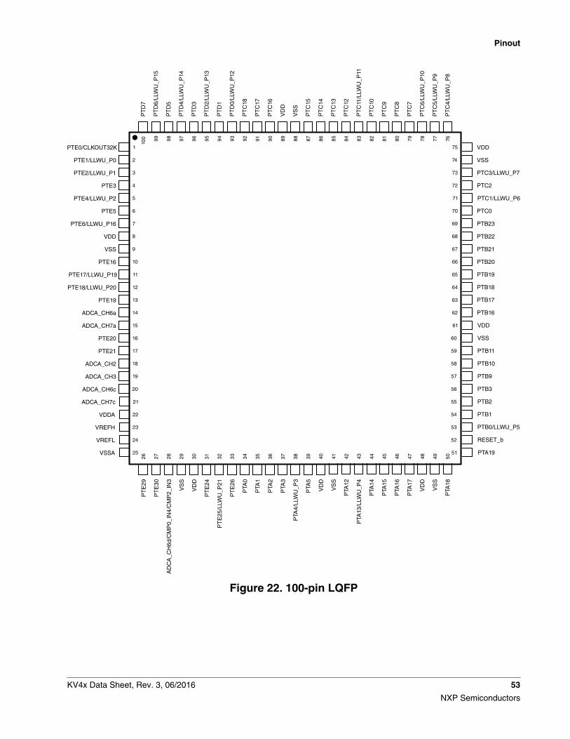
60
59
58
57
56
55
54
53
52
51
20
19
18
17
16
15
14
13
12
11
10
9
8
7
6
5
4
3
2
1
ADCA_CH6c
ADCA_CH3
ADCA_CH2
PTE21
PTE20
ADCA_CH7a
ADCA_CH6a
PTE19
PTE18/LLWU_P20
PTE17/LLWU_P19
PTE16
VSS
VDD
PTE6/LLWU_P16
PTE5
PTE4/LLWU_P2
PTE3
PTE2/LLWU_P1
PTE1/LLWU_P0
PTE0/CLKOUT32K 75
74
73
72
71
70
69
68
67
66
65
64
63
62
61
VDD
VSS
PTC3/LLWU_P7
PTC2
PTC1/LLWU_P6
PTC0
PTB23
PTB22
PTB21
PTB20
PTB19
PTB18
PTB17
PTB16
VDD
VSS
PTB11
PTB10
PTB9
PTB3
PTB2
PTB1
PTB0/LLWU_P5
RESET_b
PTA1925
24
23
22
21
VSSA
VREFL
VREFH
VDDA
ADCA_CH7c
403938373635343332313029282726
99 79 78 77 76
PT
D6/
LLW
U_P
15
PT
C7
PT
C6/
LLW
U_P
10
PT
C5/
LLW
U_P
9
PT
C4/
LLW
U_P
850494847464544434241
PTA
18
VS
S
VD
D
PTA
17
PTA
16
PTA
15
PTA
14
PTA
13/L
LWU
_P4
PTA
12
VS
S
VD
D
PTA
5
PTA
4/LL
WU
_P3
PTA
3
PTA
2
PTA
1
PTA
0
PT
E26
PT
E25
/LLW
U_P
21
PT
E24
VD
D
VS
S
AD
CA
_CH
6d/C
MP
0_IN
4/C
MP
2_IN
3
PT
E30
PT
E29
98P
TD
5
97P
TD
4/LL
WU
_P14
96P
TD
3
95P
TD
2/LL
WU
_P13
94P
TD
1
93P
TD
0/LL
WU
_P12
92P
TC
18
91P
TC
17
90P
TC
16
89V
DD
88V
SS
80P
TC
8
PT
C9
PT
C10
818283P
TC
11/L
LWU
_P11
84P
TC
12
85P
TC
13
86P
TC
14
87P
TC
15
100
PT
D7
Figure 22. 100-pin LQFP
Pinout
KV4x Data Sheet, Rev. 3, 06/2016 53
NXP Semiconductors
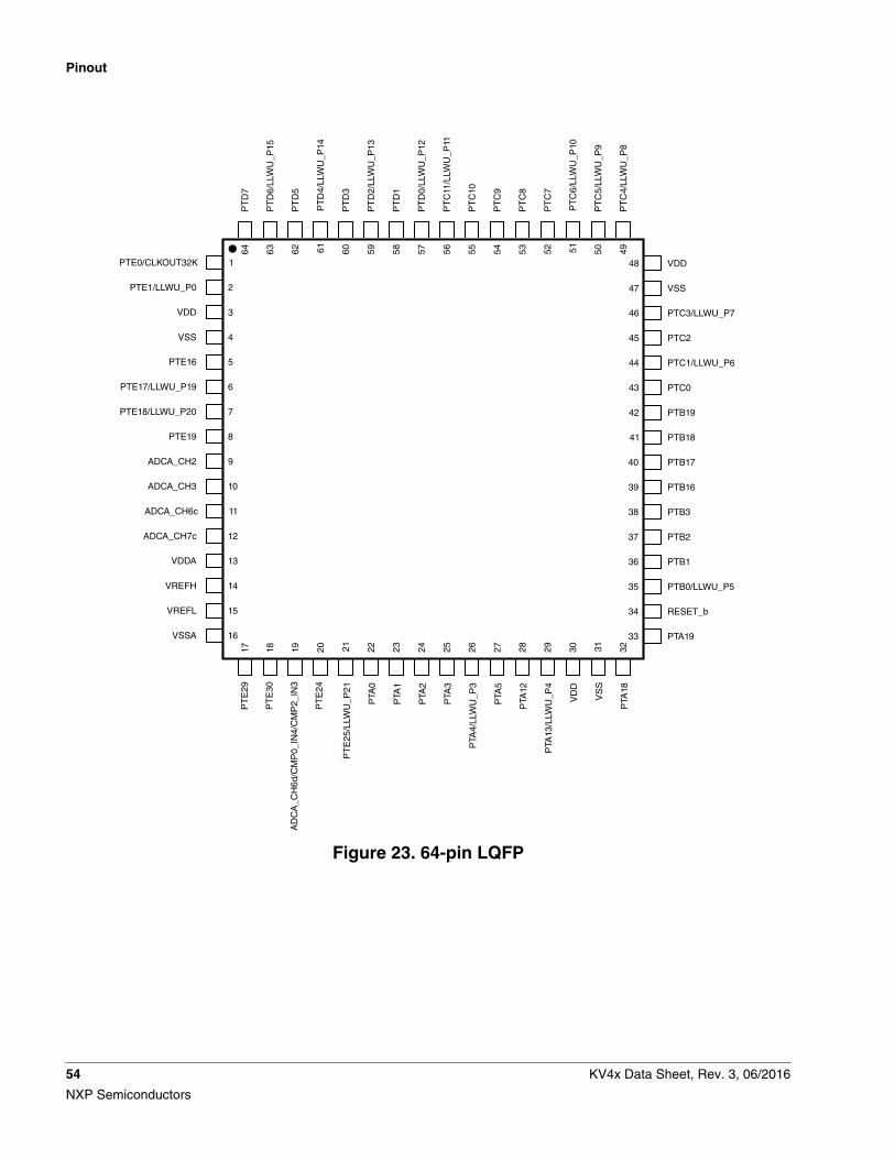
PT
E24
AD
CA
_CH
6d/C
MP
0_IN
4/C
MP
2_IN
3
PT
E30
PT
E29
VSSA
VREFL
VREFH
VDDA
ADCA_CH7c
ADCA_CH6c
ADCA_CH3
ADCA_CH2
PTE19
PTE18/LLWU_P20
PTE17/LLWU_P19
PTE16
VSS
VDD
PTE1/LLWU_P0
PTE0/CLKOUT32K
60 59 58 57 56 55 54 53 52 51 50 49
48
47
46
45
44
43
42
41
40
39
38
37
36
35
34
33
32313029282726252423222120191817
16
15
14
13
12
11
10
9
8
7
6
5
4
3
2
1
64 63 62 61
PT
D7
PT
D6/
LLW
U_P
15
PT
D5
PT
D4/
LLW
U_P
14
PT
D3
PT
D2/
LLW
U_P
13
PT
D1
PT
D0/
LLW
U_P
12
PT
C11
/LLW
U_P
11
PT
C10
PT
C9
PT
C8
PT
C7
PT
C6/
LLW
U_P
10
PT
C5/
LLW
U_P
9
PT
C4/
LLW
U_P
8
VDD
VSS
PTC3/LLWU_P7
PTC2
PTC1/LLWU_P6
PTC0
PTB19
PTB18
PTB17
PTB16
PTB3
PTB2
PTB1
PTB0/LLWU_P5
RESET_b
PTA19P
TA18
VS
S
VD
D
PTA
13/L
LWU
_P4
PTA
12
PTA
5
PTA
4/LL
WU
_P3
PTA
3
PTA
2
PTA
1
PTA
0
PT
E25
/LLW
U_P
21
Figure 23. 64-pin LQFP
Pinout
54 KV4x Data Sheet, Rev. 3, 06/2016
NXP Semiconductors
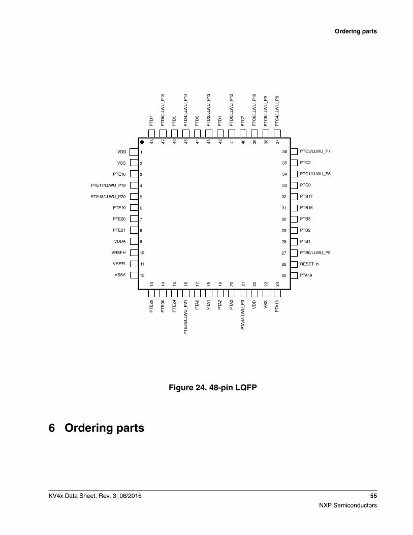
VSSA
VREFL
VREFH
VDDA
PTE21
PTE20
PTE19
PTE18/LLWU_P20
PTE17/LLWU_P19
PTE16
VSS
VDD
12
11
10
9
8
7
6
5
4
3
2
148 47 46 45 44 43 42 41 40 39 38 37
PT
D7
PT
D6/
LLW
U_P
15
PT
D5
PT
D4/
LLW
U_P
14
PT
D3
PT
D2/
LLW
U_P
13
PT
D1
PT
D0/
LLW
U_P
12
PT
C7
PT
C6/
LLW
U_P
10
PT
C5/
LLW
U_P
9
PT
C4/
LLW
U_P
8
36
35
34
33
PTC3/LLWU_P7
PTC2
PTC1/LLWU_P6
PTC0
32
31
30
29
28
27
26
25
PTB17
PTB16
PTB3
PTB2
PTB1
PTB0/LLWU_P5
RESET_b
PTA19
PTA
3
PTA
2
PTA
1
PTA
0
2423222120191817
PT
E25
/LLW
U_P
21
PT
E24
PT
E30
PT
E29
16151413
PTA
18
VS
S
VD
D
PTA
4/LL
WU
_P3
Figure 24. 48-pin LQFP
6 Ordering parts
Ordering parts
KV4x Data Sheet, Rev. 3, 06/2016 55
NXP Semiconductors
6.1 Determining valid orderable parts
Valid orderable part numbers are provided on the web. To determine the orderable partnumbers for this device, go to www.nxp.com and perform a part number search for theMKV4x device numbers.
7 Part identification
7.1 Description
Part numbers for the chip have fields that identify the specific part. You can use thevalues of these fields to determine the specific part you have received.
7.2 Format
Part numbers for this device have the following format:
Q KV## A FFF T PP CC S N
7.3 Fields
This table lists the possible values for each field in the part number (not allcombinations are valid):
Field Description Values
Q Qualification status • M = Fully qualified, general market flow• P = Prequalification
KV## Kinetis family • KV42• KV44• KV46
A Key attribute • F = Cortex-M4 w/ DSP and FPU
FFF Program flash memory size • 64 = 64 KB• 128 = 128 KB• 256 = 256 KB
T Temperature range (°C) • V = –40 to 105
PP Package identifier • LF = 48 LQFP (7 mm x 7 mm)• LH = 64 LQFP (10 mm x 10 mm)• LL = 100 LQFP (14 mm x 14 mm)
CC Maximum CPU frequency (MHz) • 16 = 168 MHz
Table continues on the next page...
Part identification
56 KV4x Data Sheet, Rev. 3, 06/2016
NXP Semiconductors
Field Description Values
S Software type • P = KMS-PMSM and BLDC• (Blank) = Not software enabled
N Packaging type • R = Tape and reel• (Blank) = Trays
7.4 Example
This is an example part number:
MKV46F256VLL16
8 Terminology and guidelines
8.1 Definition: Operating requirement
An operating requirement is a specified value or range of values for a technicalcharacteristic that you must guarantee during operation to avoid incorrect operationand possibly decreasing the useful life of the chip.
8.1.1 Example
This is an example of an operating requirement:
Symbol Description Min. Max. Unit
VDD 1.0 V core supplyvoltage
0.9 1.1 V
8.2 Definition: Operating behavior
Unless otherwise specified, an operating behavior is a specified value or range ofvalues for a technical characteristic that are guaranteed during operation if you meetthe operating requirements and any other specified conditions.
Terminology and guidelines
KV4x Data Sheet, Rev. 3, 06/2016 57
NXP Semiconductors
8.2.1 Example
This is an example of an operating behavior:
Symbol Description Min. Max. Unit
IWP Digital I/O weak pullup/pulldown current
10 130 µA
8.3 Definition: Attribute
An attribute is a specified value or range of values for a technical characteristic that areguaranteed, regardless of whether you meet the operating requirements.
8.3.1 Example
This is an example of an attribute:
Symbol Description Min. Max. Unit
CIN_D Input capacitance:digital pins
— 7 pF
8.4 Definition: Rating
A rating is a minimum or maximum value of a technical characteristic that, if exceeded,may cause permanent chip failure:
• Operating ratings apply during operation of the chip.• Handling ratings apply when the chip is not powered.
8.4.1 Example
This is an example of an operating rating:
Symbol Description Min. Max. Unit
VDD 1.0 V core supplyvoltage
–0.3 1.2 V
Terminology and guidelines
58 KV4x Data Sheet, Rev. 3, 06/2016
NXP Semiconductors
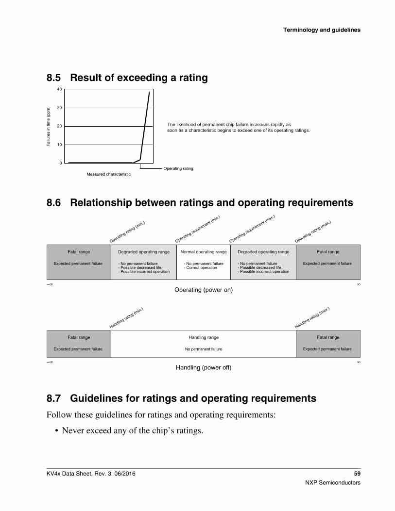
8.5 Result of exceeding a rating40
30
20
10
0
Measured characteristicOperating rating
Failu
res
in ti
me
(ppm
)
The likelihood of permanent chip failure increases rapidly as soon as a characteristic begins to exceed one of its operating ratings.
8.6 Relationship between ratings and operating requirements
–∞
- No permanent failure- Correct operation
Normal operating rangeFatal range
Expected permanent failure
Fatal range
Expected permanent failure
∞
Operating rating (max.)
Operating requirement (max.)
Operating requirement (min.)
Operating rating (min.)
Operating (power on)
Degraded operating range Degraded operating range
–∞
No permanent failure
Handling rangeFatal range
Expected permanent failure
Fatal range
Expected permanent failure
∞
Handling rating (max.)
Handling rating (min.)
Handling (power off)
- No permanent failure- Possible decreased life- Possible incorrect operation
- No permanent failure- Possible decreased life- Possible incorrect operation
8.7 Guidelines for ratings and operating requirements
Follow these guidelines for ratings and operating requirements:
• Never exceed any of the chip’s ratings.
Terminology and guidelines
KV4x Data Sheet, Rev. 3, 06/2016 59
NXP Semiconductors
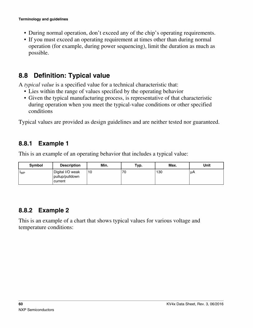
• During normal operation, don’t exceed any of the chip’s operating requirements.• If you must exceed an operating requirement at times other than during normal
operation (for example, during power sequencing), limit the duration as much aspossible.
8.8 Definition: Typical valueA typical value is a specified value for a technical characteristic that:
• Lies within the range of values specified by the operating behavior• Given the typical manufacturing process, is representative of that characteristic
during operation when you meet the typical-value conditions or other specifiedconditions
Typical values are provided as design guidelines and are neither tested nor guaranteed.
8.8.1 Example 1
This is an example of an operating behavior that includes a typical value:
Symbol Description Min. Typ. Max. Unit
IWP Digital I/O weakpullup/pulldowncurrent
10 70 130 µA
8.8.2 Example 2
This is an example of a chart that shows typical values for various voltage andtemperature conditions:
Terminology and guidelines
60 KV4x Data Sheet, Rev. 3, 06/2016
NXP Semiconductors
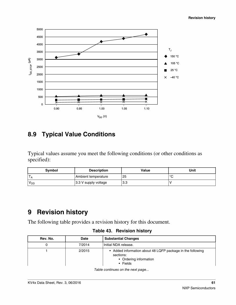
0.90 0.95 1.00 1.05 1.100
500
1000
1500
2000
2500
3000
3500
4000
4500
5000
150 °C
105 °C
25 °C
–40 °C
VDD (V)
I(μ
A)D
D_S
TOP
TJ
8.9 Typical Value Conditions
Typical values assume you meet the following conditions (or other conditions asspecified):
Symbol Description Value Unit
TA Ambient temperature 25 °C
VDD 3.3 V supply voltage 3.3 V
9 Revision historyThe following table provides a revision history for this document.
Table 43. Revision history
Rev. No. Date Substantial Changes
0 7/2014 Initial NDA release.
1 2/2015 • Added information about 48 LQFP package in the followingsections:
• Ordering information• Fields
Table continues on the next page...
Revision history
KV4x Data Sheet, Rev. 3, 06/2016 61
NXP Semiconductors
Table 43. Revision history (continued)
Rev. No. Date Substantial Changes
• Obtaining package dimensions• Pinout
• In table "Power consumption operating behaviors", removed thetext "Maximum core fequency of 150 Mhz" from note for IDDA.
• In table "Typical device clock specifications", removed informationabout High Speed run mode.
2 8/2015 • Updated instances of operating frequency from 150 MHz to 168Mhz
• Changed document number from "KV4XP100M150" to"KV4XP100M168" due to the change in operating frequency
• Part numbers ending with "15" changed to ending with "16"• Removed instances of MKV45, MKV43, and MKV40 part
numbers• Updated MKV41 part numbers to MKV42• Added part numbers MKV44F256VLL16 and MKV44F256VLH16• Updated table "Orderable part numbers summary"• In table Recommended Operating Conditions :
• Updated minimum digital supply voltage to 1.71 V• Added footnote numbers 2 and 3• Removed rows for IOH, IOL, NF, TR, and tFLRET
• Updated table Voltage and current operating behaviors• Updated table Power mode transition operating behaviors• Updated table Power consumption operating behaviors• Updated table EMC radiated emissions operating behaviors• Updated table Typical device clock specifications• Updated table Thermal attributes• Updated the PLL section of table MCG specifications• Updated tersall value in table Flash timing specifications —
commands• Added note to section 12-bit cyclic Analog-to-Digital Converter
(ADC) parameters• Updated IDDA_DACL P and IDDA_DACH P values in table 12-bit DAC
operating behaviors• Updated the pinouts• Added section Enhanced NanoEdge PWM characteristics
3 06/2016 • Changed occurences of Freescale to NXP• In the features list, added a section for "Kinetis Motor Suite"• Added section Kinetis Motor Suite (KMS)• In table 12-bit ADC electrical specifications, changed typical value
of ENOB from 9.5 to 9.1
Revision history
62 KV4x Data Sheet, Rev. 3, 06/2016
NXP Semiconductors
How to Reach Us:
Home Page:nxp.com
Web Support:nxp.com/support
Information in this document is provided solely to enable system and softwareimplementers to use NXP products. There are no express or implied copyrightlicenses granted hereunder to design or fabricate any integrated circuits basedon the information in this document. NXP reserves the right to make changeswithout further notice to any products herein.
NXP makes no warranty, representation, or guarantee regarding the suitability ofits products for any particular purpose, nor does NXP assume any liability arisingout of the application or use of any product or circuit, and specifically disclaimsany and all liability, including without limitation consequential or incidentaldamages. “Typical” parameters that may be provided in NXP data sheets and/orspecifications can and do vary in different applications, and actual performancemay vary over time. All operating parameters, including “typicals,” must bevalidated for each customer application by customer's technical experts. NXPdoes not convey any license under its patent rights nor the rights of others. NXPsells products pursuant to standard terms and conditions of sale, which can befound at the following address: nxp.com/SalesTermsandConditions.
NXP, the NXP logo, NXP SECURE CONNECTIONS FOR A SMARTERWORLD, Freescale, the Freescale logo, and Kinetis are trademarks of NXP B.V.All other product or service names are the property of their respective owners.ARM, the ARM Powered logo, and Cortex are registered trademarks of ARMLimited (or its subsidiaries) in the EU and/or elsewhere. All rights reserved.
©2014–2016 NXP B.V.
Document Number KV4XP100M168Revision 3, 06/2016