kicad example layout (2010-05-05) - university of...
TRANSCRIPT

KiCad Example Layout (2010-05-05)Wien Bridge OscillatorUniversity of HartfordCollege of Engineering, Technology, and Architecture
This tutorial to KiCad walks you through steps to produce the layout for a Wien Bridge type oscillator. This is the second of several documents that provide a complete end to end example use of KiCad. These tutorials are written in a way to provide you with a “quick start” in using KiCad, assuming that KiCad is already installed on your computer.
This document is not comprehensive, as providing an excess of details would be distracting the mission of this document. With regard to being comprehensive, the reader is referred to the help documentation installed with KiCad. This document corresponds to KiCad version (2010-05-05 BZR 2356)-stable. The author information, copyright notice, and version date are at the end of this document.
Start The first step in producing a layout from a schematic is producing the corresponding net list. The document “KiCad Example Schematic (2010-05-05) Wien Bridge Oscillator” involves producing the schematic. A program called Cvpcb is used to assign the so-called footprints to each component . A footprint is an outline that represents a physical component used in performing the layout. The next step is to produce the layout and various plots.
Start KiCad and load the corresponding schematic into the schematic editor. The details are in the “KiCad Example Schematic (2010-05-05) Wien Bridge Oscillator” document.
Produce a Net ListThe next step is to produce the net list. In the schematic capture tool do the following:
• Click-p on the 'Netlist generation' icon
'Netlist generation' icon
• Click the 'Pcbnew' tab and click the 'Netlist' button• In the navigation window click 'Save'
Planning the LayoutThe following is the general outline for this layout:
1. Decide what the overall concept of the PC board will be2. Plan the initial placement and pick a board size3. Various considerations regarding sizing and footprint selection4. Place the components into the layout area and draw the PC board edges5. Orient the components6. Use copper traces to connect the networks7. Insert additional artwork

Overall Concept, Initial Placement, and Board SizeThe first steps are most important. To start off on this project I used the actual components to provide inspiration. Take a moment to review your data sheets and also measure the actual components, to verify that you have the units right. The figure below shows some components and the scale I used.
Sample components beside a scale
I next reviewed the schematic and arranged the components that I have onto a piece of graph paper.
Circuit Schematic
Some general observations are the that circuit involves only one integrated circuit, low power resistors, perhaps ¼ Watt or smaller, and low value capacitors. We can fit everything onto one small PC board. There is no need for hardware such as a case or heat sink.

The following is a summary of the decisions that I made for this project.
• We will produce a PC board with two copper layers, that is a top and bottom.• Only so called 'through-hole' components will be used, that is components having leads that are
inserted through holes in the PC board.• There will not be any additional layers such as a solder mask or silk screening.• While the layout tool does have the automatic routing capability, given the relative simplicity,
we will perform a so-called manual layout.• We will be using a milling machine to actually fabricate the PC board.• Mounting hardware or mounting holes will not be considered.
Next, attempt what we call, the initial component placement, or rather, deciding where to place the components on the PC board. Placement is important as the positioning and orientation of each component can make the difference between a simple layout and a challenging one. Use the schematic to inspire your first attempt. Consider taking a pencil and paper and making a sketch like that below. To get a better feel for the placement, consider using cardboard or foam shapes.
Sketch of initial component placement
I also arranged the actual parts on a sheet of graph paper and along with the sketch I arbitrarily chose to make the PC board 2.5 inches long and 2 inches high. At this moment you can produce a ball-park estimate of how much it will cost to produce the PC board. If you are considering having your PC board manufactured, companies such as Alberta Printed Circuits provide a prototype price estimator. Their URL is as follows: http://www.apcircuits.com/
Sizing ConsiderationsThere are several considerations involving board fabrication that involve either what is practical or what you are willing to pay for.
• Minimum and maximum PC board dimensions – Such dimensions might vary from 0.25 inch square to 14 x 17 inches

• Minimum feature width – The smallest dimension of item that will remain on the board. The width of a copper trace is an example of such a feature dimension.
• Minimum space between features – The minimum space between tracks, tracks and pads, or pad to pad. KiCad can watch out for the minimum spacing in your design. To set the minimum acceptable spacing value, pull down and open the Design Rules page. The default minimum clearance is 0.01 inches which provides some margin over most manufacturers.
• The number and sizes of drill bits – Some manufacturers provide a list of commonly used drill sizes and charge a modest fee for using other sizes.
• Special considerations – The LPKF milling machine is not capable of the same accuracy as a manufacturer. If you are not using such a milling machine then skip the next two sections.
Sizing Considerations Involving a Milling MachineA milling machine is essentially a two dimensional plotter and router. The following observations are based on experience on using KiCad with our LPKF milling machine with the EasyContact system. In preparing a layout I suggest the following steps be taken:
• First select footprints with larger pads. The R3-LARGE_PADS footprint has 0.0650 inch diameter pads.
• For other parts use the module editor to create a library containing such footprints. The details are given in this document.
• Choose which holes in the layout will receive a rivet and use the module editor to change the drill sizes for those components. This is also described below.
The following provides further details regarding our milling machine. The size of a pad provides a practical limit on the size of the drill that can be used.
• The pad size associated with some footprints are quite modest. The R3 footprint includes two holes that 0.0320 inches in diameter and each has pads 0.0550 inches in diameter. With the hole centered the surrounding pad material is nominally only 0.0115 inches wide.
• There is a limited number of drill sizes. The Starter Package, includes the following drill sizes.
LPKF Starter Package (p/n 102368-1) Drill Sizes – mm(inch)
• 0.5 (0.0197)• 0.6 (0.0236)• 0.7 (0.0276)
• 0.8 (0.0315)• 0.9 (0.0354)• 1.0 (0.0394)
• 1.5 (0.0591)• 2.95 (0.1161)• 3.0 (0.1181)

• To provide something similar to plated through holes, we use the EasyContact system which uses small rivets. The following values are given and recommended by LPKF.
EasyContac Rivet Sizes: mm(inch)Internaldiameter
Externaldiameter
Collardiameter
Length Drill holediameter
0.6 (0.0236) 0.8 (0.0315) 1.3 (0.0512) 2.2 (0.0866) 0.9 (0.0354)0.8 (0.0315) 1.0 (0.0394) 1.6 (0.0630) 2.2 (0.0866) 1.1 (0.0433)1.0 (0.0394) 1.4 (0.0551) 2.2 (0.0866) 2.5 (0.0984) 1.5 (0.0591)1.2 (0.0472) 1.8 (0.0709) 2.6 (0.1024) 2.6 (0.1024) 1.7 (0.0669)
To use this system the size of some holes must be increased significantly to accomdate the diameter of the rivet body and the pad size must also be increased to accomdate the collar diameter which would otherwise overhang and possibly contact other components.
Creating a Custom Footprint LibraryThe layout tool includes a modest footprint editor that can be used to:
• Edit footprints and produce a new library, which we will do now, or to• Edit footprints already inserted into the layout, we will do this later
To use the module editor, first start the layout tool by clicking the 'PCBnew' icon and in the layout tool click the ‘Open module editor’ icon.
'Run PCBnew' icon ‘Open module editor’ icon
In the Module Editor, click the ‘Select working library’ icon which is to the upper left. In the pop-up window select ‘discret’ and click ‘OK’.
‘Select working library’ icon
Click the ‘Load module from library’ icon. In the ‘Place Module’ window click ‘List All’. In the pop-up window scroll and select ‘C1’ then click ‘OK’. Next, click the ‘Module Properties’ icon.
‘Load module from library’ icon ‘Module Properties’ icon
In the ‘Module Properties’ window, in the ‘Reference’ field, click the ‘Edit button’ and change the reference value to ‘C1-WIDE_PADS’ and click ‘OK’ to close the edit window and then ‘OK’. Double click the doughnut shaped pad that is about the ‘1’ symbol and in the ‘Pad Properties’ window change the ‘Shape size X’ value to 0.0650 inches and click ‘OK’. Likewise change the diameter of the pad

about the ‘2’ symbol. To refresh the view, click the ‘Redraw view’ icon.
‘Redraw view’ icon
We will save all the new footprints in a new library called ‘MyFootprints’. Click the ‘Create new library and save current module’ icon.
‘Create new library and save current module’ icon
In the ‘Save As’ window, navigate to the project folder, change the File name to ‘MyFootprints.mod’ and click ‘Save’. In the Information pop-up window click ‘OK’.
To use the contents of the new library it is necessary to add it to the library list.
• In the Layout tool, select ‘Preferences => Library’• In the ‘Current search path list’ click to select the path to the current project• In the ‘Footprint library files’ area click ‘Add’• In the navigation window, click to select ‘MyFootprints.mod’ and click ‘Open’• Click ‘OK’ and in the ‘Save Project File’ click ‘Save’.
At this point, use the module editor to change pad sizes as you did for the following footprints:
• C1V5• D3• SIL-3• SIL-2
Load each component from the ‘discret’ library as you did before and rename each footprint by appending ‘-WIDE_PADS’ to the name. With the new library being accessible, change to the ‘MyFootprints’ library before clicking the ‘Save Module in working library’ icon and ‘OK’.
‘Save Module in working library’ icon
With the new library created, close the module editor and close the layout tool.
Assigning FootprintsThe 'Cvpcb' tool is used to assign the footprints for each component, that is the outline for each component on the PC board. The tool can be started either in the project manager window or in the schematic capture tool. Click one of the 'Run Cvpcb' icons.
'Run Cvpcb' icons

If a 'Component Library Error' window appears, click OK. In the tool window, the left pane lists all the components and the right pane lists a number of footprints. The 'Display filtered list' and 'Display full list' icons control how much of the footprint list is displayed. The idea is to assign a footprint to each of the components.
'Display filtered list' and 'Display full list' icons
In the right pane click 'C1' and then click the 'View selected footprint' icon to open the 2D viewer. The 2D viewer is helpful for seeing the actual dimensions of a part.
'View selected footprint' icon
Insider the viewer window click the '3D' icon to open the 3D viewer. The 3D viewer provides a simple means to rotate the image about to better see what a component actually looks like.
'3D Display' icon
As you select different footprints, the 2D and 3D viewers are updated, so feel free to look at various component footprints.
Besides the actual size and shape, be sure to examine the pin numbering as that can vary in two ways. Check the pin ordering as well as the pin naming to make sure they both match the schematic. It is important that you get this right, now, otherwise if discover a mistake later on, it will be far more difficult to make a correction.
To assign a footprint, first click-p to select a component and then double click-p on a footprint in the right pane. The following is the footprint assignment that I used. If you do not need the extra wide pads, you can use the non-wide versions, such as C1, C1V5, and the like.
• C1, C2 – Ceramic capacitor C1-WIDE_PADS• C3, C4 – Electrolytic capacitor C1V5-WIDE_PADS• D1, D2 – Small signal diode D3-WIDE_PADS• K1 – Connector, 3 pin SIL-3-WIDE_PADS• P1 – Connector, 2 pin SIL-2-WIDE_PADS• R1, R2, R3, R4 – Resistor, 0.25 Watt, Carbon film R3-WIDE_PADS• U1 – DIP, 8 pin DIP-8__300_ELL
With the footprints assigned, save your work.
• Click File => Save As• In the navigation window click to select 'wbridge.net' and then click 'Save'

The next step is to get started with the actual layout tool.
Starting a Layout
The layout tool can be started from the project manager window by clicking the 'PCBnew' icon.
'Run PCBnew' icon
When the layout tool starts with a new project an error appears indicating that the layout file does not exist. Click-p 'OK,' then save the file.
File => Save
A layout is divided into so-called 'layers' which can represent layers of copper as well as other things. Next configure the way KiCad will interpret the layers. With the mouse select:
Design Rules => Layers Setup
• In the 'Preset Layer Groupings' field, click to open and click to select 'Two layers, Parts on Front only.'
• In the 'Coppy Layers' field click and select '2' to indicate two copper layers.• Click 'OK'.
The 'Layer Setup' window is used to configure the layers

PC Board EdgesPC board edges are simply artwork that you draw to indicate the boundaries of the PC board. As such, when performing the layout you can cross over the edges as well as move and redraw the edges as necessary. Edges simply have to be drawn at some point during the layout process. The following shows the layout with the board edges and the initial component placement.
Board edges and initial component placement
In performing the following you will be able to zoom in, zoom out, and use the sliders to reposition the display as necessary, as you did with the schematic capture tool.
• Near the top of the layout editor window, click the pull down menu and change the choice from 'Back <PgNd>' to 'PCB_Edges'
• Click the 'Add graphic line or polygon' icon
'Add graphic line or polygon' icon
• As you move the cursor in the layout area, the coordinates are displayed in the lower edge of the window. Move the cursor to where X = 1.0000 and Y = 1.0000 and click-p to start drawing
• Move to X = 3.5000 and Y = 1.0000 and click-p to place a corner• Move to X = 3.5000 and Y = 3.0000 and click-p to place a corner• Move to X = 1.0000 and Y = 3.0000 and click-p to place a corner• Move to X = 1.0000 and Y = 1.0000, click-R and pick 'End Drawing'• Click the arrow icon to exit the add line mode
'Arrow' icon
Reading the Netlist and Initial PlacementTo read the netlist do the following:
• Click the 'Read Netlist' icon. You can float the cursor above an icon so that a hint appears.
'Read Netlist' icon
• In the 'Netlist Dialog' window click the 'Browse Netlist Files.' button and in the navigation window, click on 'wbridge.net' and click-p on 'Open'.
• In the 'Netlist Dialog' window click the 'Read Current Netlist' button then click 'Close'
At this moment all the component footprints are in a pile, in the the upper left of the layout area. You will move the components one at a time, to the upper left area of the page, arranging the components according to your sketch.
• Point the cursor at a component and press the 'M' key to grab a component• Once grabbed, the component stays with the cursor• Click-p with the mouse to place the component• While still grabbed, click the 'R' key to rotate the component
The initial placement is essentially guesswork. Click the 'Show board ratsnest' icon, which provides a visual indication of how adjacent components are connected.
'Show board ratsnest' icon
To be able to see the component identifiers more clearly, in the right pane, click the 'Render' tab and unselect the box for 'Hidden text.'
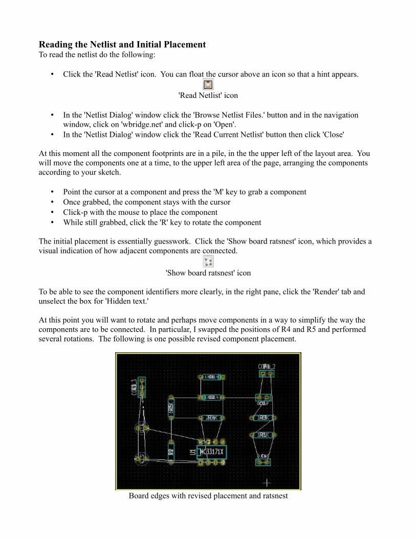
At this point you will want to rotate and perhaps move components in a way to simplify the way the components are to be connected. In particular, I swapped the positions of R4 and R5 and performed several rotations. The following is one possible revised component placement.
Board edges with revised placement and ratsnest
Tracks for Ground and PowerThe power and ground networks can be the most challenging part of your layout, so it is important to devise a plan early on. In general terms, the power and ground networks should represent low impedance pathways. This means that the ground network will provide a uniform reference voltage to all the components. Likewise the power networks will each provide consistent power.
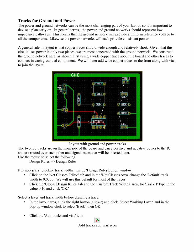
A general rule in layout is that copper traces should wide enough and relatively short. Given that this circuit uses power in only two places, we are most concerned with the ground network. We construct the ground network here, as shown, first using a wide copper trace about the board and other traces to connect in each grounded component. We will later add wide copper traces to the front along with vias to join the layers.
Layout with ground and power tracksThe two red tracks are on the front side of the board and carry positive and negative power to the IC, and are routed over each other and signal traces that will be inserted later.Use the mouse to select the following:
Design Rules => Design Rules
It is necessary to define track widths. In the 'Design Rules Editor' window• Click on the 'Net Classes Editor' tab and in the 'Net Classes Area' change the 'Default' track
width to 0.0250. We will use this default for most of the traces• Click the 'Global Design Rules' tab and the 'Custom Track Widths' area, for 'Track 1' type in the
value 0.10 and click 'OK.'
Select a layer and track width before drawing a trace. • In the layout area, click the right button (click-r) and click 'Select Working Layer' and in the
pop-up window click to select 'Back', then OK.
• Click the 'Add tracks and vias' icon
'Add tracks and vias' icon

• Move the cursor into the layout area, click-r, and select 'Select Track Width' and select 0.025”
In starting a track it is important to identify what network the track corresponds to. Be sure to tart or end a track either at a component pin or another existing track.
• Point the cursor at the middle pin in the three pin connector K1 and click-p• Move the cursor to left, 0.1” from the board edge• Click-r and pick 'End Track'
Use the copper tracing to draw a box just inside the PC board edges that will be for ground.• Change the track width to 0.1”, move the cursor to the left end of the new trace and click-p• Move the cursor 0.1” to the right of and 0.1” below the upper left corner and click-p• Move the cursor 0.1” to the left of and 0.1” below the upper right corner and click-p• Move the cursor 0.1” to the left of and 0.1” above the lower right corner and click-p• Move the cursor back to the starting point, right click and select 'End Track'
Add additional ground wiring• Click the 'Highlight net' icon, point to the ground trace and click-p to highlight ground pins
'Highlight net' icon
• Start the tracks and vias tool, change the track width to 0.025”• Add a short track from each component pin connected to ground, to the adjacent ground track
With the placement for connector K1 and capacitors C3 and C4, at least one power track will be on the front side of the board. I opted to have several tracks on the front side.
• The first track is on the back side. Start the tool, select the back side, and change the track width to 0.025”.
• The square pad for K1 identifies pin 1. Point and click-p pin 3 which is opposite pin 1.• Move the cursor downward and slightly right, down two pin 2 of C4. To place a bend in the
track, click-p with the mouse. Once the track is routed you can return to normal mode (click the arrow) and use the mouse to reposition the track.
• The remaining power tracks are on the front side. This time be sure to change the working layer to 'Front' before inserting the power and ground tracks.

Remaining TracksThe following shows the layout with the remaining tracks and an additional ground track on the front side, as well as vias.
Layout with remaining tracks, vias, and text inserted
To finish the layout, place a wide copper ground track about the front side of the board along with connecting holes, called vias.
• Start the track and via tool, set the track width to 0.10” and start with the back side. We start on the back side as that is where the existing ground track is.
• With the mouse, move the mouse to the upper left corner above the ground track and click-p to start the track.
• Without moving the mouse, click the 'V' on the keyboard to place a via, doing so also changes the working layer to the front side.
• Move the mouse about the corners, placing bends, and ending the track as you did before.• I have a via inserted at each corner of the board as well as midpoint along each edge. To insert
a via, point and click to start a track, but without moving the mouse click 'V' on the keyboard and then right click 'End Track.'
Inserting TextTo insert text, pick a layer and click the 'Add text' icon, move the cursor to where text will be inserted, and click-p to open the 'Add text' window. I set the text width to 0.013”.
'Add text' iconI inserted the following text:
◦ The title on the front ' Wien-Bridge Osc.'◦ Identifying text for the front or top component side, 'Top'◦ Identifying text for the back or bottom side, and mirrored, 'Btm'◦ If this as an assignment then include your name and date on the front side as well

Resizing HolesRather than using the module editor to modify a library, we can use the module editor to modify footprints already inserted into the layout. If you are using the milling machine, then increase the following holes to accommodate the rivets through hole connectivity.
• C3 pin 1• C4 pin 2• U1 pin 4• U1 pin 7
Open the module editor as you did before, but this time:• Click the 'Load module from current board' icon, select C3, then click 'OK'.
'Load module from current board' icon
• Refer back to the EasyContac Rivet Sizes table and select a drill size. For the 0.8mm rivets use the 1.1mm or 0.0433 inch diameter drill size.
• As you did earlier, change the diameter of the hole for C3 pad 1 to 0.0433 inch
• Click the 'Update module in current board' icon
'Update module in current board' icon
• Follow the above steps to change the size of the other holes Remaining CommentsSome PC board manufactures request that alignment targets be inserted into your layout. Be sure to contact your board manufacturer and ask for their recommendation. To insert an alignment target, select a layer and then Click the 'Add layer alignment target' icon, position the cursor, then click-p. To repeat, if your board is to be manufactured, be sure to contact your manufacturer and ask questions.
In using a router machine to fabricate the board, it is important that the back side pattern be aligned with that on the top or front side of the board. One method discusssed in the next part is to drill alignment holes at known locations as part of the fabrication.
Three Dimensional ViewTo see the PC board in three dimensions, wit the mouse select:
3D Display => 3D Display
You use the mouse to rotate the image and the '+' and '–' icons to zoom in and out, respectively.

Layout rendered in 3D view
Producing Plot FilesAt this point save your layout, you are now ready to produce the plot files to fabricate your PC board. If you are going to use the milling machine then proceed to the next part of the tutorial. If your PC board will be manufactured, then be sure to review your manufacturer's literature and ask questions as to what plots are required and how to submit a job for manufacturing. Companies such as Alberta Printed Circuits provide a Windows tool that makes it convenient to submit a job for manufacturing. Their URL is as follows: http://www.apcircuits.com/
Author InformationDr. Jonathan Hill (jmhill at hartford dot edu) is an associate professor in Electrical and Computer Engineering at the University of Hartford College of Engineering, Technology, and Architecture. His interests involve embedded microprocessor based systems. This document was written in haste so please help with constructive criticism and/or send a thank-you for the effort.
Copyright NoticeCopyright (C) 2011, by Jonathan Hill Permission is granted to copy, distribute and/or modify this document under the terms of the GNU Free Documentation License, Version 1.3 or any later version published by the Free Software Foundation; with no Invariant Sections, no Front-Cover Texts, and no Back-Cover Texts. Modified versions of this document will include the current version date and all the prior version dates on which the document is based, immediately following the copyright notice. A copy of the license is available from the GNU project website at the following URL. http://www.gnu.org/licenses/fdl.html
Publication Date: Mar. 09, 2011 by Jonathan HillPrevious Version: Jan. 17, 2011 by Jonathan Hill