is29gl256 is29gl128 · 2018-09-07 · program suspend/resume and erase suspend/resume advanced...
TRANSCRIPT
IS29GL256 IS29GL128
256Mb/128Mb 3.0V PAGE MODE PARALLEL FLASH MEMORY
DATA SHEET
Integrated Silicon Solution, Inc. - www.issi.com Rev. A
08/13/2018
2
IS29GL256/128
FEATURES
Single power supply operation
- Full voltage range: 2.7 to 3.6 volts read and
write operations
Fast Access Time at -40°C to +125°C:
- 70ns (1) at Vcc = 3.0V~3.6V, VIO = 3.0V~3.6V
- VIO Input/Output 1.65V to 3.6V. - All input levels (address, control, and DQ input
levels) and outputs are determined by voltage on VIO input.
8-word/16-byte page read buffer
32-word/64-byte write buffer reduces overall
programming time for multiple-word updates
Secured Silicon Region (SSR) - 512-word/1024-byte sector for permanent,
secure identification - 256-word Factory Locked SSR and 256-word
Customer Locked SSR
Uniform 64Kword/128KByte Sector
Architecture
Suspend and Resume commands for Program
and Erase operations
Write operation status bits indicate program
and erase operation completion
Support for CFI (Common Flash Interface)
Volatile and non-volatile methods of Advanced
Sector Protection
WP#/ACC input
- Accelerates programming time (when VHH is
applied) for greater throughput during system
production
- Protects first or last sector regardless of sector
protection settings
Hardware reset input (RESET#) resets device
Ready/Busy# output (RY/BY#) detects program
or erase cycle completion
Minimum 100K program/erase endurance
cycles.
Package Options
- 56-pin TSOP
- 64-ball 13mm x 11mm BGA
- 64-ball 9mm x 9mm BGA
- 56-ball 9mm x 7mm BGA (Call Factory)
Temperature Range - Extended Grade: -40°C to +105°C - Automotive Grade: -40°C to +125°C
Note: 1. 80ns at Vcc=2.7V~3.6V, VIO=2.7V~3.6V. 90ns at Vcc=2.7V~3.6V, VIO=1.65V ~ Vcc.
GENERAL DESCRIPTION
The IS29GL256/128 offer a fast page access time of 20ns with a corresponding random access time as fast as 70ns. It features a Write Buffer that allows a maximum of 32 words/64 bytes to be programmed in one operation, resulting in faster effective programming time than standard programming algorithms. This makes the device ideal for today’s embedded applications that require higher density, better performance and lower power consumption.
IS29GL256/128 256/128 Megabit Flash Memory Page mode Flash Memory, CMOS 3.0 Volt-only
PRELIMINARY INFORMATION
Integrated Silicon Solution, Inc. - www.issi.com Rev. A
08/13/2018
3
IS29GL256/128
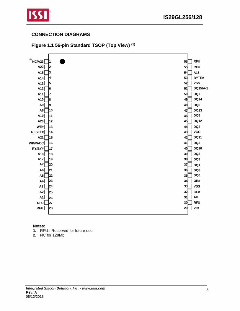
CONNECTION DIAGRAMS Figure 1.1 56-pin Standard TSOP (Top View) (1)
A15
A14
A13
A12
A11
A10
A9
A8
A19
A20
WE#
RESET#
A21
WP#/ACC
RY/BY#
A17
A7
A6
A5
A4
A16
BYTE#
VSS
DQ15/A-1
DQ7
DQ14
DQ6
DQ13
DQ5
DQ4
DQ12
VCC
DQ11
DQ3
DQ10
DQ9
DQ1
DQ8
DQ0
OE#
VSS
NC/A23
A22
RFU
RFU
A18 DQ2
A3
A2
A1
RFU
CE#
A0
RFU
VIORFU
42
41
40
39
38
37
36
35
34
33
52
51
50
49
48
47
46
45
44
43
53
55
54
56
32
31
30
29
3
4
5
6
7
8
9
10
11
12
14
13
15
16
17
18
23
24
22
21
20
19
1
2
27
28
26
25
(2)
Notes: 1. RFU= Reserved for future use
2. NC for 128Mb
Integrated Silicon Solution, Inc. - www.issi.com Rev. A
08/13/2018
4
IS29GL256/128
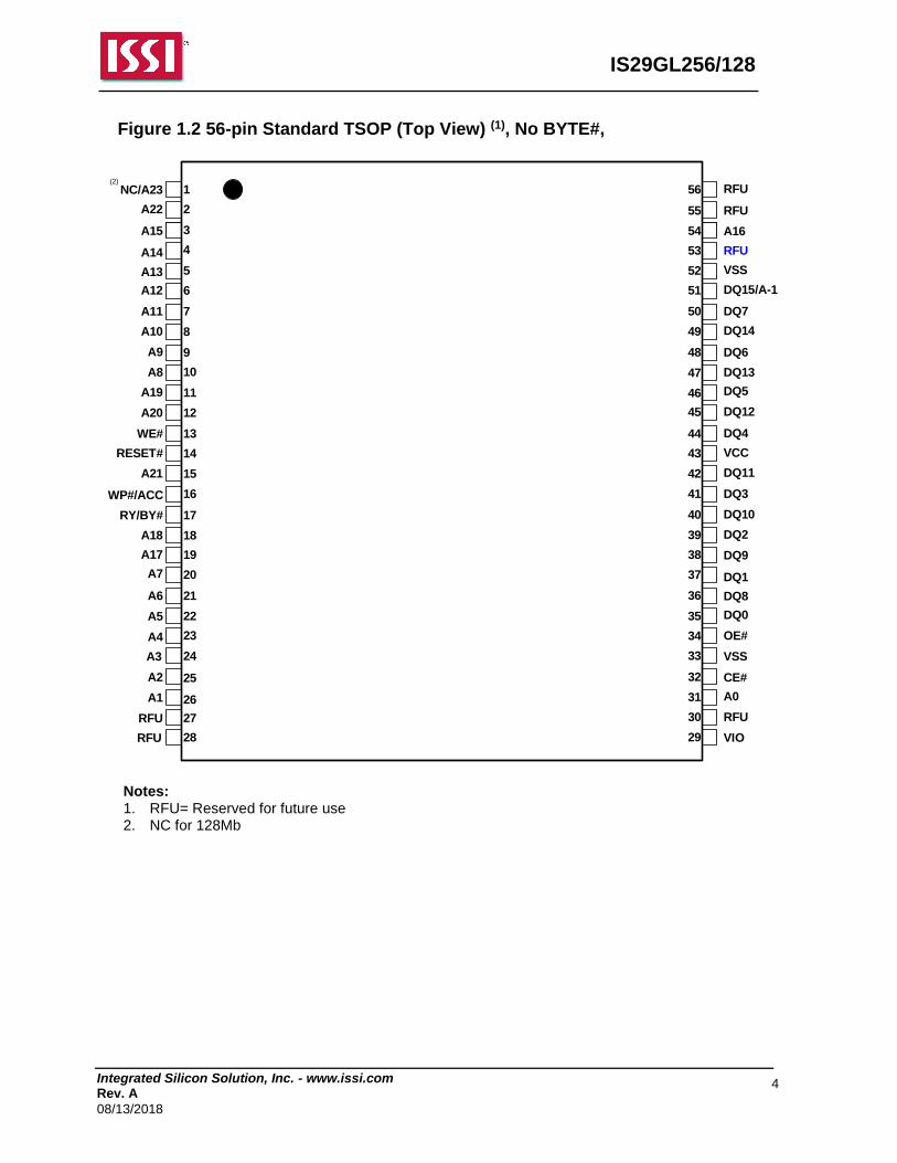
Figure 1.2 56-pin Standard TSOP (Top View) (1), No BYTE#,
A15
A14
A13
A12
A11
A10
A9
A8
A19
A20
WE#
RESET#
A21
WP#/ACC
RY/BY#
A17
A7
A6
A5
A4
A16
RFU
VSS
DQ15/A-1
DQ7
DQ14
DQ6
DQ13
DQ5
DQ4
DQ12
VCC
DQ11
DQ3
DQ10
DQ9
DQ1
DQ8
DQ0
OE#
VSS
NC/A23
A22
RFU
RFU
A18 DQ2
A3
A2
A1
RFU
CE#
A0
RFU
VIORFU
42
41
40
39
38
37
36
35
34
33
52
51
50
49
48
47
46
45
44
43
53
55
54
56
32
31
30
29
3
4
5
6
7
8
9
10
11
12
14
13
15
16
17
18
23
24
22
21
20
19
1
2
27
28
26
25
(2)
Notes: 1. RFU= Reserved for future use
2. NC for 128Mb
Integrated Silicon Solution, Inc. - www.issi.com Rev. A
08/13/2018
5
IS29GL256/128
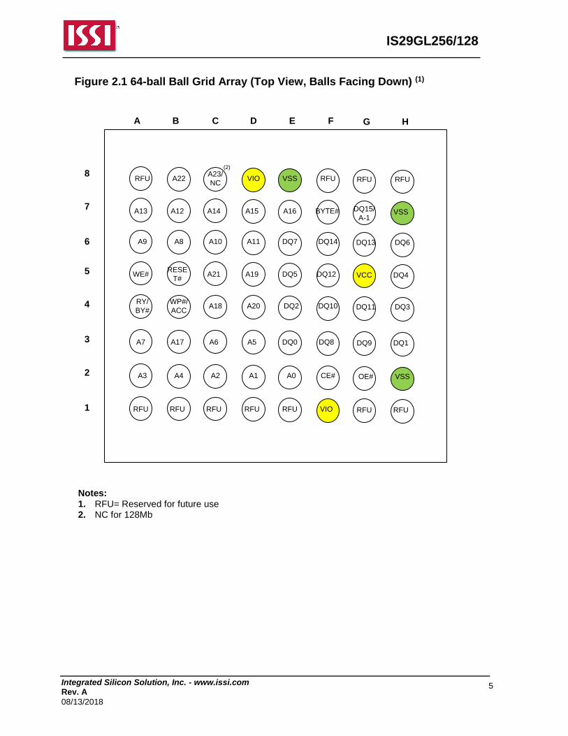
Figure 2.1 64-ball Ball Grid Array (Top View, Balls Facing Down) (1)
RFUA23/
NCA22 VIO VSS RFU
A13 A14A12 A15 A16 BYTE#
A9 A10A8 A11 DQ7 DQ14
WE# A21RESE
T#A19 DQ5 DQ12
RY/
BY#A18
WP#/
ACCA20 DQ2 DQ10
A7 A6A17 A5 DQ0 DQ8
A3 A2A4 A1 A0 CE#
RFU RFURFU RFU RFU VIO
A B C D E F
8
7
6
5
4
3
2
1
RFU RFU
DQ15/
A-1VSS
DQ13 DQ6
VCC DQ4
DQ11 DQ3
DQ9 DQ1
OE# VSS
RFU RFU
G H
(2)
Notes: 1. RFU= Reserved for future use
2. NC for 128Mb
Integrated Silicon Solution, Inc. - www.issi.com Rev. A
08/13/2018
6
IS29GL256/128
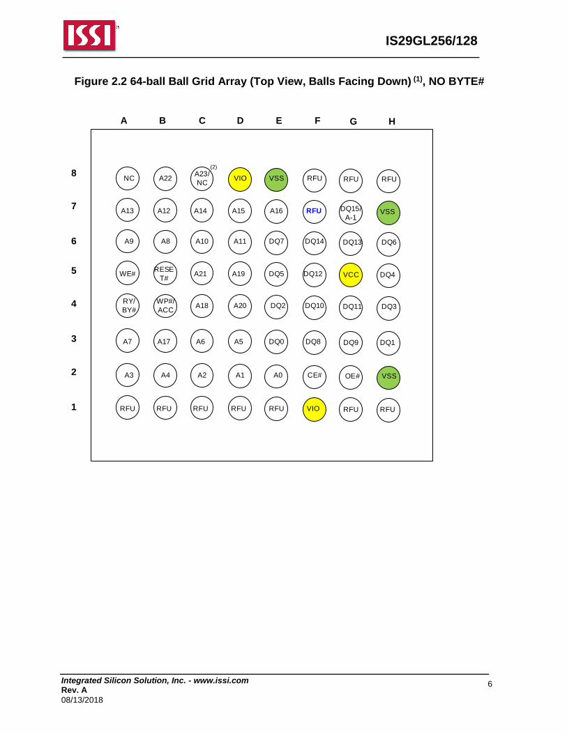
Figure 2.2 64-ball Ball Grid Array (Top View, Balls Facing Down) (1), NO BYTE#
NCA23/
NCA22 VIO VSS RFU
A13 A14A12 A15 A16 RFU
A9 A10A8 A11 DQ7 DQ14
WE# A21RESE
T#A19 DQ5 DQ12
RY/
BY#A18
WP#/
ACCA20 DQ2 DQ10
A7 A6A17 A5 DQ0 DQ8
A3 A2A4 A1 A0 CE#
RFU RFURFU RFU RFU VIO
A B C D E F
8
7
6
5
4
3
2
1
RFU RFU
DQ15/
A-1VSS
DQ13 DQ6
VCC DQ4
DQ11 DQ3
DQ9 DQ1
OE# VSS
RFU RFU
G H
(2)
Integrated Silicon Solution, Inc. - www.issi.com Rev. A
08/13/2018
7
IS29GL256/128
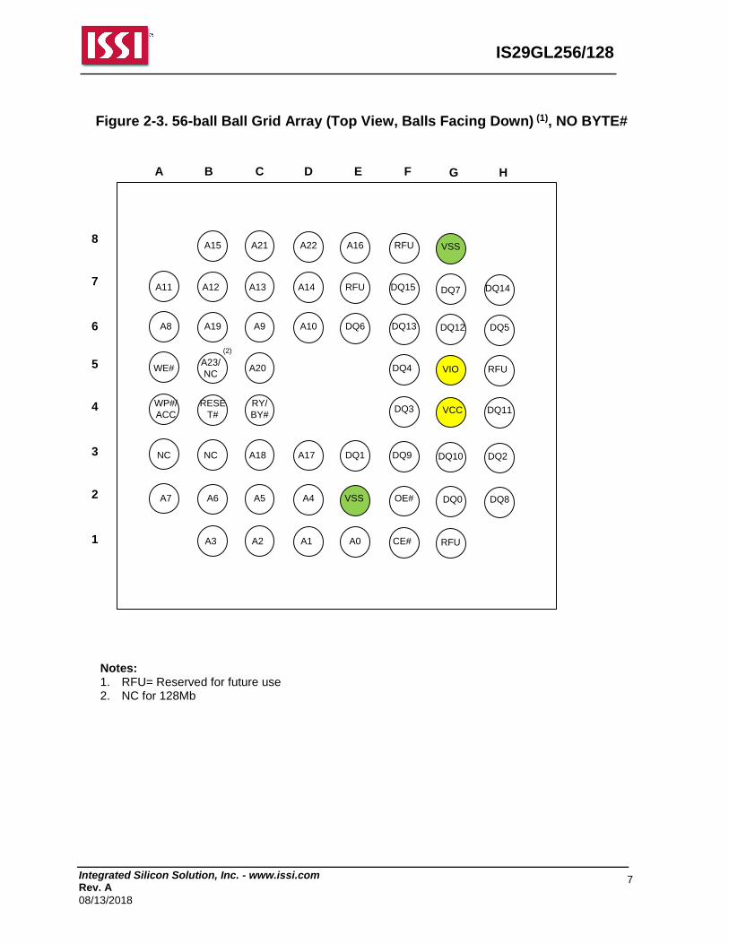
Figure 2-3. 56-ball Ball Grid Array (Top View, Balls Facing Down) (1), NO BYTE#
A21A15 A22 A16 RFU
A11 A13A12 A14 RFU DQ15
A8 A9A19 A10 DQ6 DQ13
WE# A20A23/
NCDQ4
WP#/
ACC
RY/
BY#
RESE
T#DQ3
NC A18NC A17 DQ1 DQ9
A7 A5A6 A4 VSS OE#
A2A3 A1 A0 CE#
A B C D E F
8
7
6
5
4
3
2
1
VSS
DQ7 DQ14
DQ12 DQ5
VIO RFU
VCC DQ11
DQ10 DQ2
DQ0 DQ8
RFU
G H
(2)
Notes: 1. RFU= Reserved for future use
2. NC for 128Mb
Integrated Silicon Solution, Inc. - www.issi.com Rev. A
08/13/2018
8
IS29GL256/128
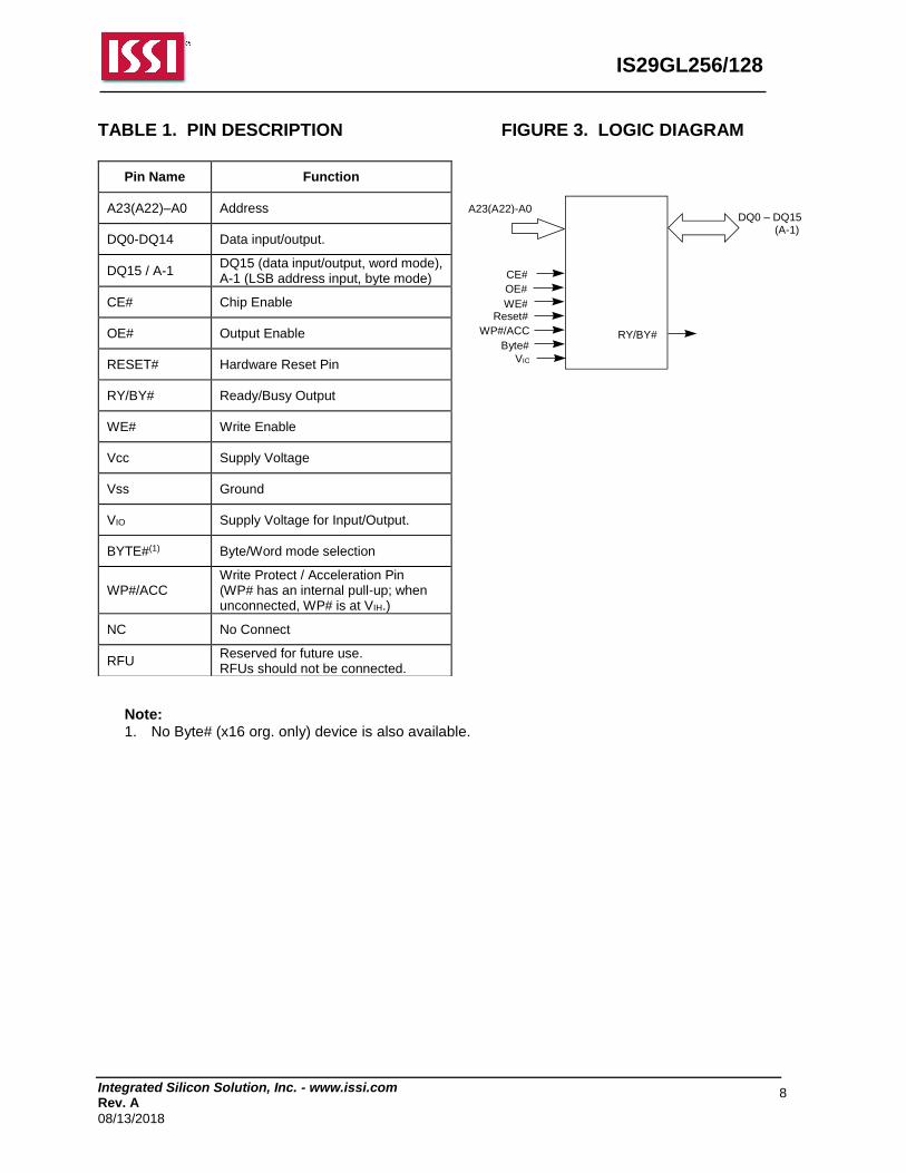
TABLE 1. PIN DESCRIPTION FIGURE 3. LOGIC DIAGRAM
Note: 1. No Byte# (x16 org. only) device is also available.
Pin Name Function
A23(A22)–A0 Address
DQ0-DQ14 Data input/output.
DQ15 / A-1 DQ15 (data input/output, word mode), A-1 (LSB address input, byte mode)
CE# Chip Enable
OE# Output Enable
RESET# Hardware Reset Pin
RY/BY# Ready/Busy Output
WE# Write Enable
Vcc Supply Voltage
Vss Ground
VIO Supply Voltage for Input/Output.
BYTE#(1) Byte/Word mode selection
WP#/ACC Write Protect / Acceleration Pin (WP# has an internal pull-up; when unconnected, WP# is at VIH.)
NC No Connect
RFU Reserved for future use. RFUs should not be connected.
DQ0 – DQ15 (A-1)
A23(A22)-A0
WE#
CE#
RY/BY#
Reset#
Byte#
OE#
WP#/ACC
VIO
Integrated Silicon Solution, Inc. - www.issi.com Rev. A
08/13/2018
9
IS29GL256/128
Table 2. PRODUCT SELECTOR GUIDE
Product Number IS29GL256/128
Maximum SPEED 70ns(1) at Vcc = 3.0V ~ 3.6V, VIO = 3.0V ~ 3.6V
Temperature
Extended (E) -40°C to +105°C
Automotive (A3) 40°C to +125°C
Note:
1. Maximum speed becomes 80ns when Vcc = 2.7V ~ 3.6V, VIO = 2.7V ~ 3.6V, and 90ns when Vcc = 2.7V ~ 3.6V, VIO = 1.65V~Vcc.
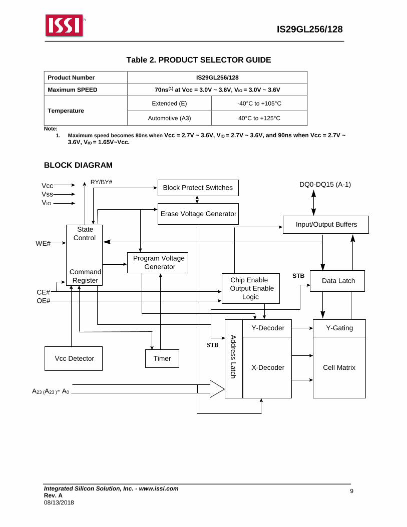
BLOCK DIAGRAM
WE#
CE# OE#
State Control
Command Register
Erase Voltage Generator Input/Output Buffers
Program Voltage Generator
Chip Enable Output Enable
Logic
Data Latch
Y-Decoder
X-Decoder
Y-Gating
Cell Matrix Timer Vcc Detector
A23 (A23 )- A0
Vcc Vss
DQ0-DQ15 (A-1) A
dd
ress L
atc
h
Block Protect Switches
STB
STB
RY/BY#
VIO
Integrated Silicon Solution, Inc. - www.issi.com Rev. A
08/13/2018
10
IS29GL256/128
Product Overview
IS29GL256/128 are 256/128 Mb, page mode Flash devices optimized for today’s embedded designs that demand a large storage array and rich functionality. This product offers uniform 64 Kword (128 KB) sectors and feature VI/O control, allowing control and I/O signals to operate from 1.65 V to VCC. Additional features include:
Single word programming or a 32-word buffer for an increased programming speed
Program Suspend/Resume and Erase Suspend/Resume
Advanced Sector Protection methods for protecting sectors as required
512 words/1024 bytes of Secured Silicon Region for storing customer secured information. The Secured Silicon Region is One Time Programmable (OTP).
Integrated Silicon Solution, Inc. - www.issi.com Rev. A
08/13/2018
11
IS29GL256/128
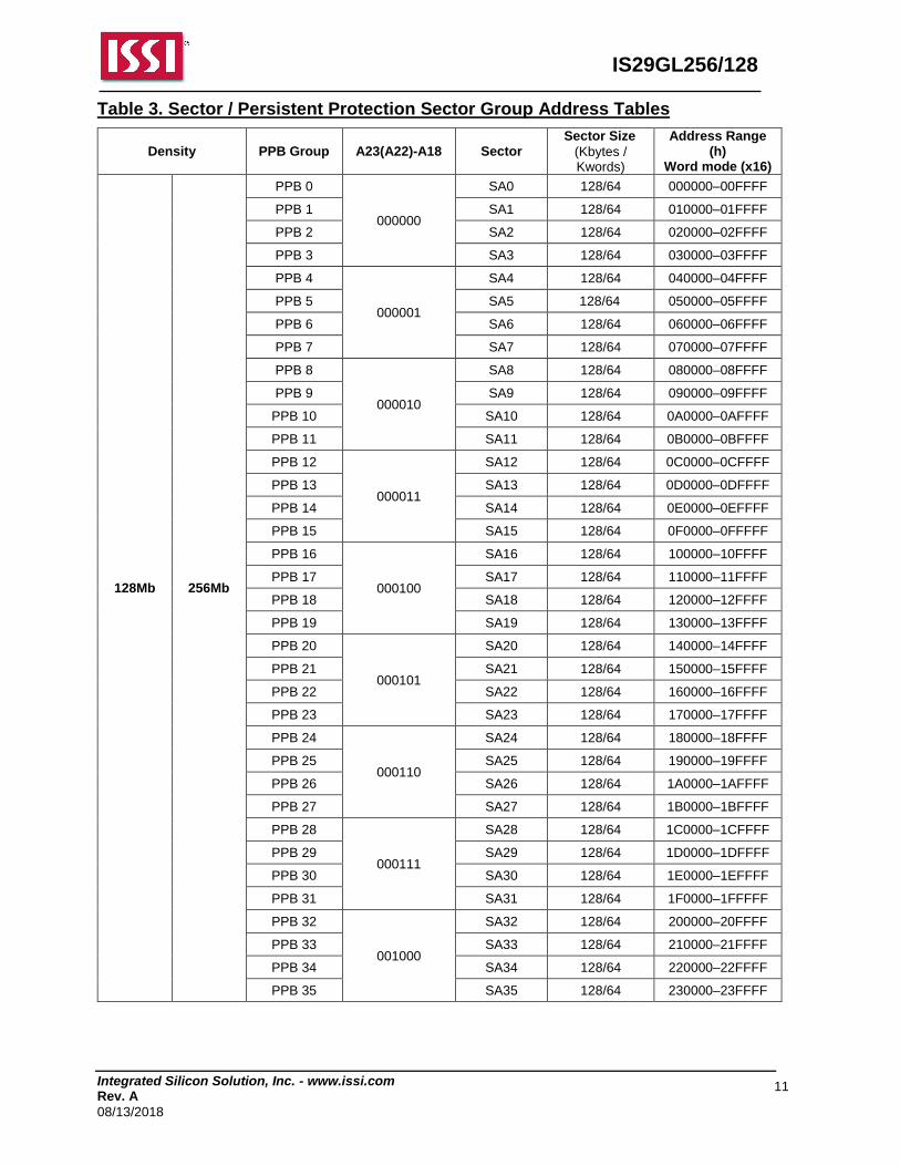
Table 3. Sector / Persistent Protection Sector Group Address Tables
Density PPB Group A23(A22)-A18 Sector Sector Size
(Kbytes / Kwords)
Address Range (h)
Word mode (x16)
128Mb 256Mb
PPB 0
000000
SA0 128/64 000000–00FFFF
PPB 1 SA1 128/64 010000–01FFFF
PPB 2 SA2 128/64 020000–02FFFF
PPB 3 SA3 128/64 030000–03FFFF
PPB 4
000001
SA4 128/64 040000–04FFFF
PPB 5 SA5 128/64 050000–05FFFF
PPB 6 SA6 128/64 060000–06FFFF
PPB 7 SA7 128/64 070000–07FFFF
PPB 8
000010
SA8 128/64 080000–08FFFF
PPB 9 SA9 128/64 090000–09FFFF
PPB 10 SA10 128/64 0A0000–0AFFFF
PPB 11 SA11 128/64 0B0000–0BFFFF
PPB 12
000011
SA12 128/64 0C0000–0CFFFF
PPB 13 SA13 128/64 0D0000–0DFFFF
PPB 14 SA14 128/64 0E0000–0EFFFF
PPB 15 SA15 128/64 0F0000–0FFFFF
PPB 16
000100
SA16 128/64 100000–10FFFF
PPB 17 SA17 128/64 110000–11FFFF
PPB 18 SA18 128/64 120000–12FFFF
PPB 19 SA19 128/64 130000–13FFFF
PPB 20
000101
SA20 128/64 140000–14FFFF
PPB 21 SA21 128/64 150000–15FFFF
PPB 22 SA22 128/64 160000–16FFFF
PPB 23 SA23 128/64 170000–17FFFF
PPB 24
000110
SA24 128/64 180000–18FFFF
PPB 25 SA25 128/64 190000–19FFFF
PPB 26 SA26 128/64 1A0000–1AFFFF
PPB 27 SA27 128/64 1B0000–1BFFFF
PPB 28
000111
SA28 128/64 1C0000–1CFFFF
PPB 29 SA29 128/64 1D0000–1DFFFF
PPB 30 SA30 128/64 1E0000–1EFFFF
PPB 31 SA31 128/64 1F0000–1FFFFF
PPB 32
001000
SA32 128/64 200000–20FFFF
PPB 33 SA33 128/64 210000–21FFFF
PPB 34 SA34 128/64 220000–22FFFF
PPB 35 SA35 128/64 230000–23FFFF
Integrated Silicon Solution, Inc. - www.issi.com Rev. A
08/13/2018
12
IS29GL256/128
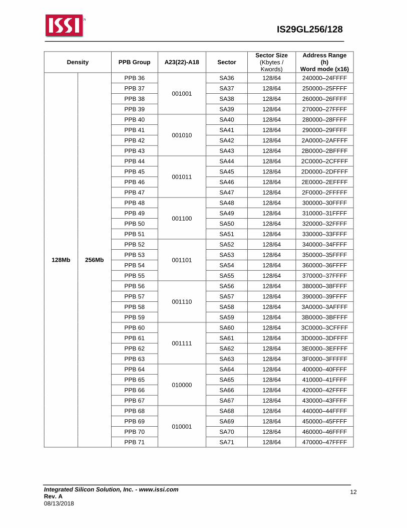
Density PPB Group A23(22)-A18 Sector Sector Size
(Kbytes / Kwords)
Address Range (h)
Word mode (x16)
128Mb 256Mb
PPB 36
001001
SA36 128/64 240000–24FFFF
PPB 37 SA37 128/64 250000–25FFFF
PPB 38 SA38 128/64 260000–26FFFF
PPB 39 SA39 128/64 270000–27FFFF
PPB 40
001010
SA40 128/64 280000–28FFFF
PPB 41 SA41 128/64 290000–29FFFF
PPB 42 SA42 128/64 2A0000–2AFFFF
PPB 43 SA43 128/64 2B0000–2BFFFF
PPB 44
001011
SA44 128/64 2C0000–2CFFFF
PPB 45 SA45 128/64 2D0000–2DFFFF
PPB 46 SA46 128/64 2E0000–2EFFFF
PPB 47 SA47 128/64 2F0000–2FFFFF
PPB 48
001100
SA48 128/64 300000–30FFFF
PPB 49 SA49 128/64 310000–31FFFF
PPB 50 SA50 128/64 320000–32FFFF
PPB 51 SA51 128/64 330000–33FFFF
PPB 52
001101
SA52 128/64 340000–34FFFF
PPB 53 SA53 128/64 350000–35FFFF
PPB 54 SA54 128/64 360000–36FFFF
PPB 55 SA55 128/64 370000–37FFFF
PPB 56
001110
SA56 128/64 380000–38FFFF
PPB 57 SA57 128/64 390000–39FFFF
PPB 58 SA58 128/64 3A0000–3AFFFF
PPB 59 SA59 128/64 3B0000–3BFFFF
PPB 60
001111
SA60 128/64 3C0000–3CFFFF
PPB 61 SA61 128/64 3D0000–3DFFFF
PPB 62 SA62 128/64 3E0000–3EFFFF
PPB 63 SA63 128/64 3F0000–3FFFFF
PPB 64
010000
SA64 128/64 400000–40FFFF
PPB 65 SA65 128/64 410000–41FFFF
PPB 66 SA66 128/64 420000–42FFFF
PPB 67 SA67 128/64 430000–43FFFF
PPB 68
010001
SA68 128/64 440000–44FFFF
PPB 69 SA69 128/64 450000–45FFFF
PPB 70 SA70 128/64 460000–46FFFF
PPB 71 SA71 128/64 470000–47FFFF
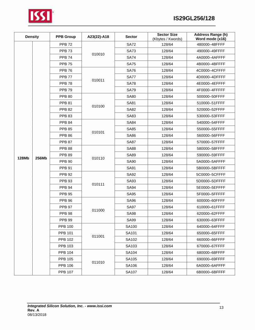
Integrated Silicon Solution, Inc. - www.issi.com Rev. A
08/13/2018
13
IS29GL256/128
Density PPB Group A23(22)-A18 Sector Sector Size
(Kbytes / Kwords)
Address Range (h) Word mode (x16)
128Mb 256Mb
PPB 72
010010
SA72 128/64 480000–48FFFF
PPB 73 SA73 128/64 490000–49FFFF
PPB 74 SA74 128/64 4A0000–4AFFFF
PPB 75 SA75 128/64 4B0000–4BFFFF
PPB 76
010011
SA76 128/64 4C0000–4CFFFF
PPB 77 SA77 128/64 4D0000–4DFFFF
PPB 78 SA78 128/64 4E0000–4EFFFF
PPB 79 SA79 128/64 4F0000–4FFFFF
PPB 80
010100
SA80 128/64 500000–50FFFF
PPB 81 SA81 128/64 510000–51FFFF
PPB 82 SA82 128/64 520000–52FFFF
PPB 83 SA83 128/64 530000–53FFFF
PPB 84
010101
SA84 128/64 540000–54FFFF
PPB 85 SA85 128/64 550000–55FFFF
PPB 86 SA86 128/64 560000–56FFFF
PPB 87 SA87 128/64 570000–57FFFF
PPB 88
010110
SA88 128/64 580000–58FFFF
PPB 89 SA89 128/64 590000–59FFFF
PPB 90 SA90 128/64 5A0000–5AFFFF
PPB 91 SA91 128/64 5B0000–5BFFFF
PPB 92
010111
SA92 128/64 5C0000–5CFFFF
PPB 93 SA93 128/64 5D0000–5DFFFF
PPB 94 SA94 128/64 5E0000–5EFFFF
PPB 95 SA95 128/64 5F0000–5FFFFF
PPB 96
011000
SA96 128/64 600000–60FFFF
PPB 97 SA97 128/64 610000–61FFFF
PPB 98 SA98 128/64 620000–62FFFF
PPB 99 SA99 128/64 630000–63FFFF
PPB 100
011001
SA100 128/64 640000–64FFFF
PPB 101 SA101 128/64 650000–65FFFF
PPB 102 SA102 128/64 660000–66FFFF
PPB 103 SA103 128/64 670000–67FFFF
PPB 104
011010
SA104 128/64 680000–68FFFF
PPB 105 SA105 128/64 690000–69FFFF
PPB 106 SA106 128/64 6A0000–6AFFFF
PPB 107 SA107 128/64 6B0000–6BFFFF

Integrated Silicon Solution, Inc. - www.issi.com Rev. A
08/13/2018
14
IS29GL256/128
Density PPB Group A23(22)-A18 Sector Sector Size
(Kbytes / Kwords)
Address Range (h) Word mode (x16)
128Mb
256Mb
PPB 108
011011
SA108 128/64 6C0000–6CFFFF
PPB 109 SA109 128/64 6D0000–6DFFFF
PPB 110 SA110 128/64 6E0000–6EFFFF
PPB 111 SA111 128/64 6F0000–6FFFFF
PPB 112
011100
SA112 128/64 700000–70FFFF
PPB 113 SA113 128/64 710000–71FFFF
PPB 114 SA114 128/64 720000–72FFFF
PPB 115 SA115 128/64 730000–73FFFF
PPB 116
011101
SA116 128/64 740000–74FFFF
PPB 117 SA117 128/64 750000–75FFFF
PPB 118 SA118 128/64 760000–76FFFF
PPB 119 SA119 128/64 770000–77FFFF
PPB 120
011110
SA120 128/64 780000–78FFFF
PPB 121 SA121 128/64 790000–79FFFF
PPB 122 SA122 128/64 7A0000–7AFFFF
PPB 123 SA123 128/64 7B0000–7BFFFF
PPB 124
011111
SA124 128/64 7C0000–7CFFFF
PPB 125 SA125 128/64 7D0000–7DFFFF
PPB 126 SA126 128/64 7E0000–7EFFFF
PPB 127 SA127 128/64 7F0000–7FFFFF
PPB 128
100000
SA128 128/64 800000–80FFFF
PPB 129 SA129 128/64 810000–81FFFF
PPB 130 SA130 128/64 820000–82FFFF
PPB 131 SA131 128/64 830000–83FFFF
PPB 132
100001
SA132 128/64 840000–84FFFF
PPB 133 SA133 128/64 850000–85FFFF
PPB 134 SA134 128/64 860000–86FFFF
PPB 135 SA135 128/64 870000–87FFFF
PPB 136
100010
SA136 128/64 880000–88FFFF
PPB 137 SA137 128/64 890000–89FFFF
PPB 138 SA138 128/64 8A0000–8AFFFF
PPB 139 SA139 128/64 8B0000–8BFFFF
PPB 140
100011
SA140 128/64 8C0000–8CFFFF
PPB 141 SA141 128/64 8D0000–8DFFFF
PPB 142 SA142 128/64 8E0000–8EFFFF
PPB 143 SA143 128/64 8F0000–8FFFFF
Integrated Silicon Solution, Inc. - www.issi.com Rev. A
08/13/2018
15
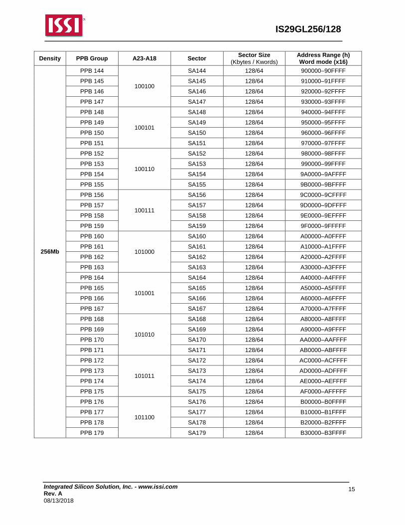
IS29GL256/128
Density PPB Group A23-A18 Sector Sector Size
(Kbytes / Kwords)
Address Range (h) Word mode (x16)
256Mb
PPB 144
100100
SA144 128/64 900000–90FFFF
PPB 145 SA145 128/64 910000–91FFFF
PPB 146 SA146 128/64 920000–92FFFF
PPB 147 SA147 128/64 930000–93FFFF
PPB 148
100101
SA148 128/64 940000–94FFFF
PPB 149 SA149 128/64 950000–95FFFF
PPB 150 SA150 128/64 960000–96FFFF
PPB 151 SA151 128/64 970000–97FFFF
PPB 152
100110
SA152 128/64 980000–98FFFF
PPB 153 SA153 128/64 990000–99FFFF
PPB 154 SA154 128/64 9A0000–9AFFFF
PPB 155 SA155 128/64 9B0000–9BFFFF
PPB 156
100111
SA156 128/64 9C0000–9CFFFF
PPB 157 SA157 128/64 9D0000–9DFFFF
PPB 158 SA158 128/64 9E0000–9EFFFF
PPB 159 SA159 128/64 9F0000–9FFFFF
PPB 160
101000
SA160 128/64 A00000–A0FFFF
PPB 161 SA161 128/64 A10000–A1FFFF
PPB 162 SA162 128/64 A20000–A2FFFF
PPB 163 SA163 128/64 A30000–A3FFFF
PPB 164
101001
SA164 128/64 A40000–A4FFFF
PPB 165 SA165 128/64 A50000–A5FFFF
PPB 166 SA166 128/64 A60000–A6FFFF
PPB 167 SA167 128/64 A70000–A7FFFF
PPB 168
101010
SA168 128/64 A80000–A8FFFF
PPB 169 SA169 128/64 A90000–A9FFFF
PPB 170 SA170 128/64 AA0000–AAFFFF
PPB 171 SA171 128/64 AB0000–ABFFFF
PPB 172
101011
SA172 128/64 AC0000–ACFFFF
PPB 173 SA173 128/64 AD0000–ADFFFF
PPB 174 SA174 128/64 AE0000–AEFFFF
PPB 175 SA175 128/64 AF0000–AFFFFF
PPB 176
101100
SA176 128/64 B00000–B0FFFF
PPB 177 SA177 128/64 B10000–B1FFFF
PPB 178 SA178 128/64 B20000–B2FFFF
PPB 179 SA179 128/64 B30000–B3FFFF
Integrated Silicon Solution, Inc. - www.issi.com Rev. A
08/13/2018
16
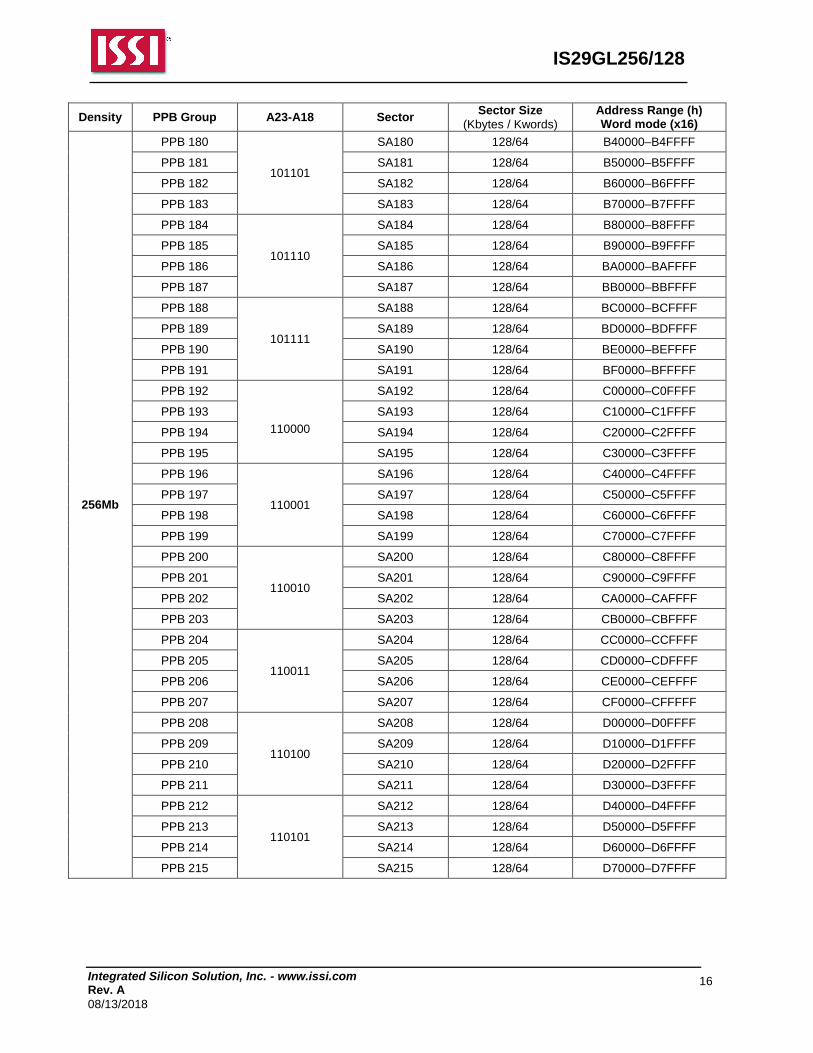
IS29GL256/128
Density PPB Group A23-A18 Sector Sector Size
(Kbytes / Kwords)
Address Range (h) Word mode (x16)
256Mb
PPB 180
101101
SA180 128/64 B40000–B4FFFF
PPB 181 SA181 128/64 B50000–B5FFFF
PPB 182 SA182 128/64 B60000–B6FFFF
PPB 183 SA183 128/64 B70000–B7FFFF
PPB 184
101110
SA184 128/64 B80000–B8FFFF
PPB 185 SA185 128/64 B90000–B9FFFF
PPB 186 SA186 128/64 BA0000–BAFFFF
PPB 187 SA187 128/64 BB0000–BBFFFF
PPB 188
101111
SA188 128/64 BC0000–BCFFFF
PPB 189 SA189 128/64 BD0000–BDFFFF
PPB 190 SA190 128/64 BE0000–BEFFFF
PPB 191 SA191 128/64 BF0000–BFFFFF
PPB 192
110000
SA192 128/64 C00000–C0FFFF
PPB 193 SA193 128/64 C10000–C1FFFF
PPB 194 SA194 128/64 C20000–C2FFFF
PPB 195 SA195 128/64 C30000–C3FFFF
PPB 196
110001
SA196 128/64 C40000–C4FFFF
PPB 197 SA197 128/64 C50000–C5FFFF
PPB 198 SA198 128/64 C60000–C6FFFF
PPB 199 SA199 128/64 C70000–C7FFFF
PPB 200
110010
SA200 128/64 C80000–C8FFFF
PPB 201 SA201 128/64 C90000–C9FFFF
PPB 202 SA202 128/64 CA0000–CAFFFF
PPB 203 SA203 128/64 CB0000–CBFFFF
PPB 204
110011
SA204 128/64 CC0000–CCFFFF
PPB 205 SA205 128/64 CD0000–CDFFFF
PPB 206 SA206 128/64 CE0000–CEFFFF
PPB 207 SA207 128/64 CF0000–CFFFFF
PPB 208
110100
SA208 128/64 D00000–D0FFFF
PPB 209 SA209 128/64 D10000–D1FFFF
PPB 210 SA210 128/64 D20000–D2FFFF
PPB 211 SA211 128/64 D30000–D3FFFF
PPB 212
110101
SA212 128/64 D40000–D4FFFF
PPB 213 SA213 128/64 D50000–D5FFFF
PPB 214 SA214 128/64 D60000–D6FFFF
PPB 215 SA215 128/64 D70000–D7FFFF
Integrated Silicon Solution, Inc. - www.issi.com Rev. A
08/13/2018
17
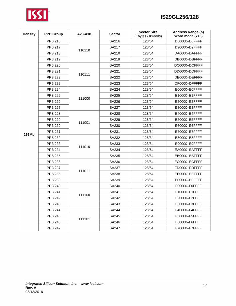
IS29GL256/128
Density PPB Group A23-A18 Sector Sector Size
(Kbytes / Kwords)
Address Range (h) Word mode (x16)
256Mb
PPB 216
110110
SA216 128/64 D80000–D8FFFF
PPB 217 SA217 128/64 D90000–D9FFFF
PPB 218 SA218 128/64 DA0000–DAFFFF
PPB 219 SA219 128/64 DB0000–DBFFFF
PPB 220
110111
SA220 128/64 DC0000–DCFFFF
PPB 221 SA221 128/64 DD0000–DDFFFF
PPB 222 SA222 128/64 DE0000–DEFFFF
PPB 223 SA223 128/64 DF0000–DFFFFF
PPB 224
111000
SA224 128/64 E00000–E0FFFF
PPB 225 SA225 128/64 E10000–E1FFFF
PPB 226 SA226 128/64 E20000–E2FFFF
PPB 227 SA227 128/64 E30000–E3FFFF
PPB 228
111001
SA228 128/64 E40000–E4FFFF
PPB 229 SA229 128/64 E50000–E5FFFF
PPB 230 SA230 128/64 E60000–E6FFFF
PPB 231 SA231 128/64 E70000–E7FFFF
PPB 232
111010
SA232 128/64 E80000–E8FFFF
PPB 233 SA233 128/64 E90000–E9FFFF
PPB 234 SA234 128/64 EA0000–EAFFFF
PPB 235 SA235 128/64 EB0000–EBFFFF
PPB 236
111011
SA236 128/64 EC0000–ECFFFF
PPB 237 SA237 128/64 ED0000–EDFFFF
PPB 238 SA238 128/64 EE0000–EEFFFF
PPB 239 SA239 128/64 EF0000–EFFFFF
PPB 240
111100
SA240 128/64 F00000–F0FFFF
PPB 241 SA241 128/64 F10000–F1FFFF
PPB 242 SA242 128/64 F20000–F2FFFF
PPB 243 SA243 128/64 F30000–F3FFFF
PPB 244
111101
SA244 128/64 F40000–F4FFFF
PPB 245 SA245 128/64 F50000–F5FFFF
PPB 246 SA246 128/64 F60000–F6FFFF
PPB 247 SA247 128/64 F70000–F7FFFF
Integrated Silicon Solution, Inc. - www.issi.com Rev. A
08/13/2018
18
IS29GL256/128
Density
PPB Group A23-A18 Sector Sector Size
(Kbytes / Kwords)
Address Range (h) Word mode (x16)
256Mb
PPB 248
111110
SA248 128/64 F80000–F8FFFF
PPB 249 SA249 128/64 F90000–F9FFFF
PPB 250 SA250 128/64 FA0000–FAFFFF
PPB 251 SA251 128/64 FB0000–FBFFFF
PPB 252
111111
SA252 128/64 FC0000–FCFFFF
PPB 253 SA253 128/64 FD0000–FDFFFF
PPB 254 SA254 128/64 FE0000–FEFFFF
PPB 255 SA255 128/64 FF0000–FFFFFF
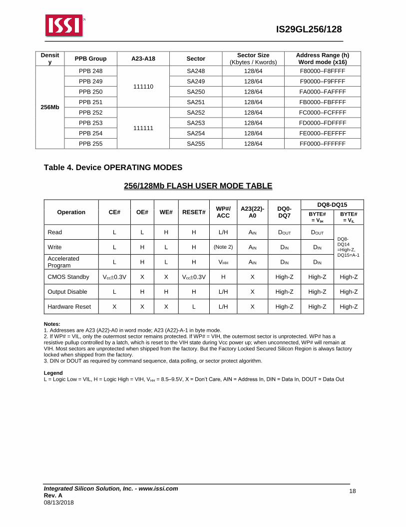
Table 4. Device OPERATING MODES
256/128Mb FLASH USER MODE TABLE
Operation CE# OE# WE# RESET# WP#/ ACC
A23(22)-A0
DQ0-DQ7
DQ8-DQ15
BYTE# = VIH
BYTE# = VIL
Read L L H H L/H AIN DOUT DOUT DQ8-DQ14 =High-Z, DQ15=A-1
Write L H L H (Note 2) AIN DIN DIN
Accelerated Program
L H L H VHH AIN DIN DIN
CMOS Standby Vcc0.3V X X Vcc0.3V H X High-Z High-Z High-Z
Output Disable L H H H L/H X High-Z High-Z High-Z
Hardware Reset X X X L L/H X High-Z High-Z High-Z
Notes: 1. Addresses are A23 (A22)-A0 in word mode; A23 (A22)-A-1 in byte mode. 2. If WP# = VIL, only the outermost sector remains protected. If WP# = VIH, the outermost sector is unprotected. WP# has a resistive pullup controlled by a latch, which is reset to the VIH state during Vcc power up; when unconnected, WP# will remain at VIH. Most sectors are unprotected when shipped from the factory. But the Factory Locked Secured Silicon Region is always factory locked when shipped from the factory. 3. DIN or DOUT as required by command sequence, data polling, or sector protect algorithm. Legend L = Logic Low = VIL, H = Logic High = VIH, VHH = 8.5–9.5V, X = Don’t Care, AIN = Address In, DIN = Data In, DOUT = Data Out
Integrated Silicon Solution, Inc. - www.issi.com Rev. A
08/13/2018
19
IS29GL256/128
USER MODE DEFINITIONS
Word / Byte Configuration The BYTE# pin controls whether the device data I/O pins operate in the byte or word configuration. If the BYTE# pin is set at logic ‘1’, the device is in word configuration, DQ0-DQ15 are active and controlled by CE#, OE#, and WE#. If the BYTE# pin is set at logic ‘0’, the device is in byte configuration, and only data I/O pins DQ0-DQ7 are active and controlled by CE#, OE#, and WE#. The data I/O pins DQ8-DQ14 are tri-stated, and the DQ15 pin is used as an input for the LSB (A-1) address function.
VIO Control The VIO allows the host system to set the voltage levels that the device generates and tolerates on all inputs and outputs (address, control, and DQ signals). VIO range is 1.65 to VCC. For example, a VIO of 1.65-3.6 volts allows for I/O at the 1.65 or 3.6 volt levels, driving and receiving signals to and from other 1.65 or 3.6 V devices on the same data bus.
Read All memories require access time to output array data. In a read operation, data is read from one memory location at a time. Addresses are presented to the device in random order, and the propagation delay through the device causes the data on its outputs to arrive with the address on its inputs. The device defaults to reading array data after device power-up or hardware reset. To read data from the memory array, the system must first assert a valid address on A23-A0, while driving OE# and CE# to VIL. WE# must remain at VIH. Data will appear on DQ15-DQ0 after address access time (tACC), which is equal to the delay from stable addresses to valid output data. The OE# signal must be driven to VIL. Data is output on DQ15-DQ0 pins after the access time (tOE) has elapsed from the falling edge of OE#, assuming the tACC access time has been meet.
Page Read Mode The device is capable of fast page mode read and is compatible with the page mode Mask ROM read operation. This mode provides faster read access speed for random locations within a page. The page size of the device is 8 words/16 bytes. The appropriate page is selected by the higher address bits A23-A3. Address bits A2-A0 in word mode (A2 to A-1 in byte mode) determine the specific word within a page. The microprocessor supplies the specific word location. The random or initial page access is equal to tACC or tCE and subsequent page read accesses (as long as the locations specified by the microprocessor falls within that page) is equivalent to tPACC. When CE# is deasserted and reasserted for a subsequent access, the access time is tACC or tCE. Fast page mode accesses are obtained by keeping the “read-page addresses” constant and changing the “intra-read page” addresses.
Integrated Silicon Solution, Inc. - www.issi.com Rev. A
08/13/2018
20
IS29GL256/128
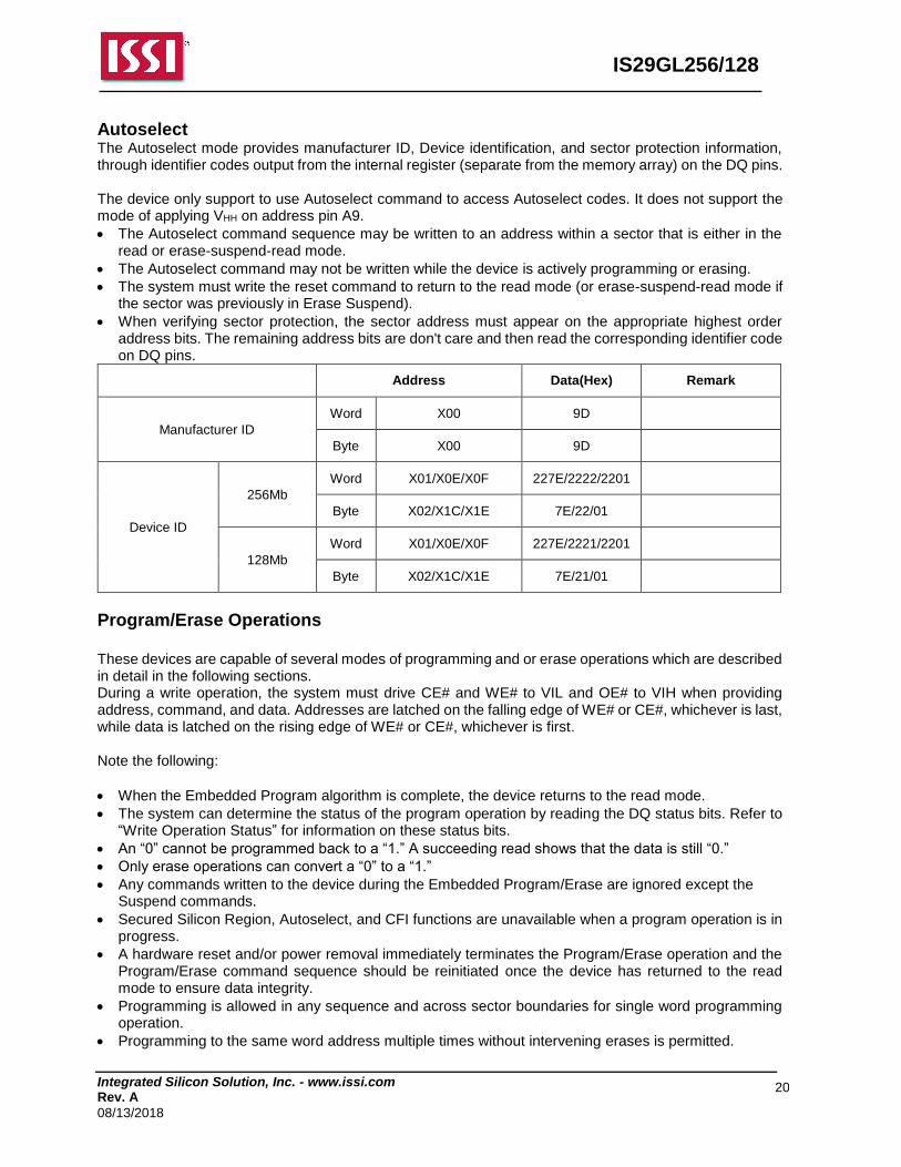
Autoselect The Autoselect mode provides manufacturer ID, Device identification, and sector protection information, through identifier codes output from the internal register (separate from the memory array) on the DQ pins. The device only support to use Autoselect command to access Autoselect codes. It does not support the mode of applying VHH on address pin A9.
The Autoselect command sequence may be written to an address within a sector that is either in the read or erase-suspend-read mode.
The Autoselect command may not be written while the device is actively programming or erasing.
The system must write the reset command to return to the read mode (or erase-suspend-read mode if the sector was previously in Erase Suspend).
When verifying sector protection, the sector address must appear on the appropriate highest order address bits. The remaining address bits are don't care and then read the corresponding identifier code on DQ pins.
Address Data(Hex) Remark
Manufacturer ID
Word X00 9D
Byte X00 9D
Device ID
256Mb
Word X01/X0E/X0F 227E/2222/2201
Byte X02/X1C/X1E 7E/22/01
128Mb
Word X01/X0E/X0F 227E/2221/2201
Byte X02/X1C/X1E 7E/21/01
Program/Erase Operations These devices are capable of several modes of programming and or erase operations which are described in detail in the following sections. During a write operation, the system must drive CE# and WE# to VIL and OE# to VIH when providing address, command, and data. Addresses are latched on the falling edge of WE# or CE#, whichever is last, while data is latched on the rising edge of WE# or CE#, whichever is first. Note the following:
When the Embedded Program algorithm is complete, the device returns to the read mode.
The system can determine the status of the program operation by reading the DQ status bits. Refer to “Write Operation Status” for information on these status bits.
An “0” cannot be programmed back to a “1.” A succeeding read shows that the data is still “0.”
Only erase operations can convert a “0” to a “1.”
Any commands written to the device during the Embedded Program/Erase are ignored except the Suspend commands.
Secured Silicon Region, Autoselect, and CFI functions are unavailable when a program operation is in progress.
A hardware reset and/or power removal immediately terminates the Program/Erase operation and the Program/Erase command sequence should be reinitiated once the device has returned to the read mode to ensure data integrity.
Programming is allowed in any sequence and across sector boundaries for single word programming operation.
Programming to the same word address multiple times without intervening erases is permitted.
Integrated Silicon Solution, Inc. - www.issi.com Rev. A
08/13/2018
21
IS29GL256/128
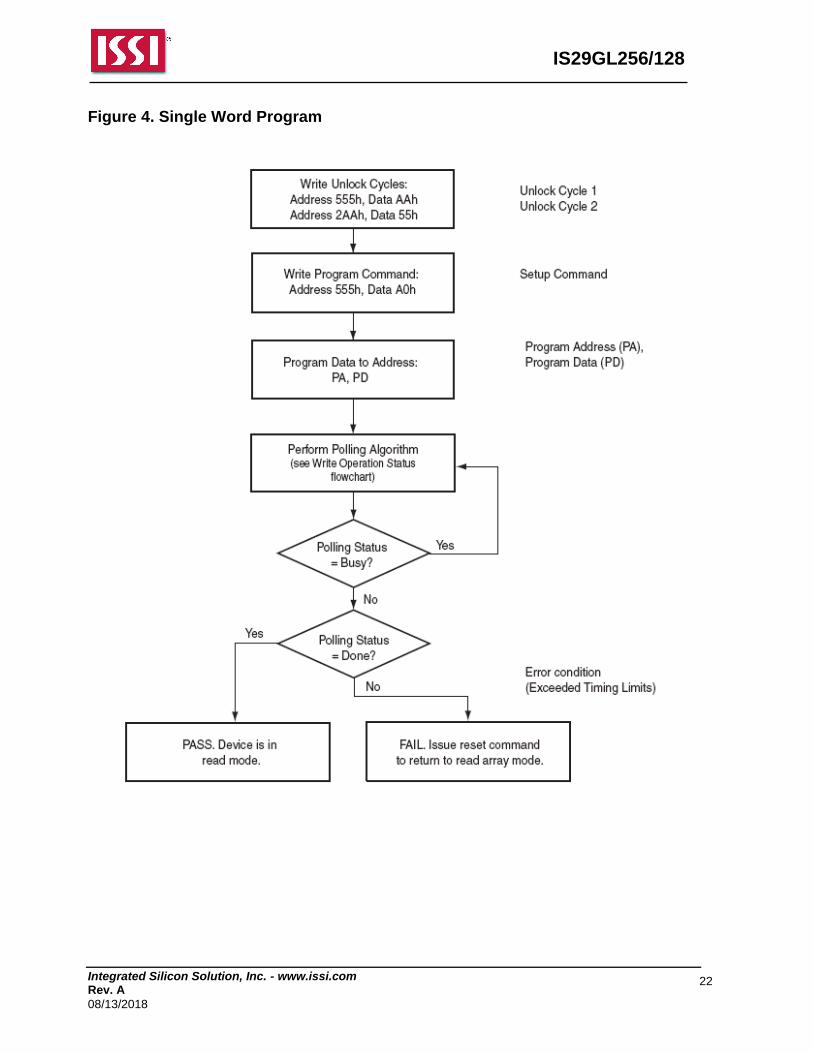
Single Word Programming Single word programming mode is one method of programming the Flash. In this mode, four Flash command write cycles are used to program an individual Flash address. The data for this programming operation could be 8 or 16-bits wide. While the single word programming method is supported by most devices, in general Single Word Programming is not recommended for devices that support Write Buffer Programming. When the Embedded Program algorithm is complete, the device then returns to the read mode and addresses are no longer latched. The system can determine the status of the program operation by reading the DQ status bits.
During programming, any command (except the Suspend command) is ignored.
The Secured Silicon Region, Autoselect, and CFI functions are unavailable when a program operation is in progress.
A hardware reset immediately terminates the program operation. The program command sequence should be reinitiated once the device has returned to the read mode, to ensure data integrity.
Programming to the same address multiple times continuously (for example, “walking” a bit within a word) is permitted.
Integrated Silicon Solution, Inc. - www.issi.com Rev. A
08/13/2018
22
IS29GL256/128
Figure 4. Single Word Program
Integrated Silicon Solution, Inc. - www.issi.com Rev. A
08/13/2018
23
IS29GL256/128
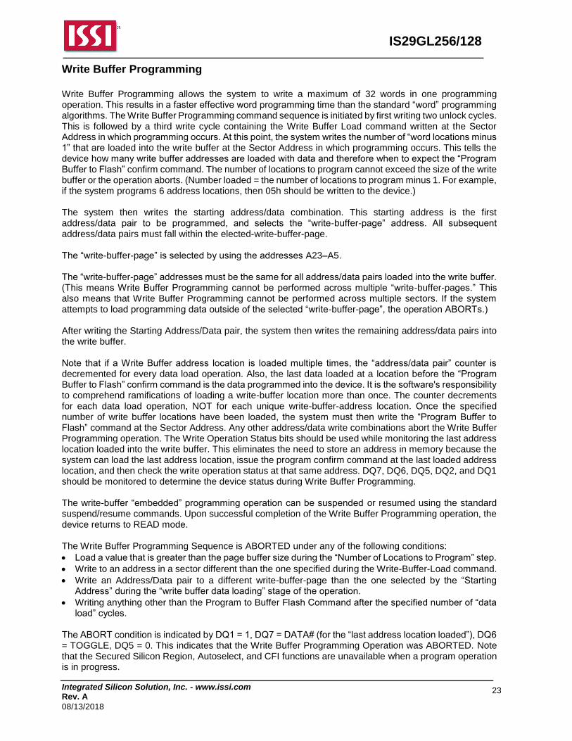
Write Buffer Programming Write Buffer Programming allows the system to write a maximum of 32 words in one programming operation. This results in a faster effective word programming time than the standard “word” programming algorithms. The Write Buffer Programming command sequence is initiated by first writing two unlock cycles. This is followed by a third write cycle containing the Write Buffer Load command written at the Sector Address in which programming occurs. At this point, the system writes the number of “word locations minus 1” that are loaded into the write buffer at the Sector Address in which programming occurs. This tells the device how many write buffer addresses are loaded with data and therefore when to expect the “Program Buffer to Flash” confirm command. The number of locations to program cannot exceed the size of the write buffer or the operation aborts. (Number loaded = the number of locations to program minus 1. For example, if the system programs 6 address locations, then 05h should be written to the device.) The system then writes the starting address/data combination. This starting address is the first address/data pair to be programmed, and selects the “write-buffer-page” address. All subsequent address/data pairs must fall within the elected-write-buffer-page. The “write-buffer-page” is selected by using the addresses A23–A5. The “write-buffer-page” addresses must be the same for all address/data pairs loaded into the write buffer. (This means Write Buffer Programming cannot be performed across multiple “write-buffer-pages.” This also means that Write Buffer Programming cannot be performed across multiple sectors. If the system attempts to load programming data outside of the selected “write-buffer-page”, the operation ABORTs.) After writing the Starting Address/Data pair, the system then writes the remaining address/data pairs into the write buffer. Note that if a Write Buffer address location is loaded multiple times, the “address/data pair” counter is decremented for every data load operation. Also, the last data loaded at a location before the “Program Buffer to Flash” confirm command is the data programmed into the device. It is the software's responsibility to comprehend ramifications of loading a write-buffer location more than once. The counter decrements for each data load operation, NOT for each unique write-buffer-address location. Once the specified number of write buffer locations have been loaded, the system must then write the “Program Buffer to Flash” command at the Sector Address. Any other address/data write combinations abort the Write Buffer Programming operation. The Write Operation Status bits should be used while monitoring the last address location loaded into the write buffer. This eliminates the need to store an address in memory because the system can load the last address location, issue the program confirm command at the last loaded address location, and then check the write operation status at that same address. DQ7, DQ6, DQ5, DQ2, and DQ1 should be monitored to determine the device status during Write Buffer Programming. The write-buffer “embedded” programming operation can be suspended or resumed using the standard suspend/resume commands. Upon successful completion of the Write Buffer Programming operation, the device returns to READ mode. The Write Buffer Programming Sequence is ABORTED under any of the following conditions:
Load a value that is greater than the page buffer size during the “Number of Locations to Program” step.
Write to an address in a sector different than the one specified during the Write-Buffer-Load command.
Write an Address/Data pair to a different write-buffer-page than the one selected by the “Starting Address” during the “write buffer data loading” stage of the operation.
Writing anything other than the Program to Buffer Flash Command after the specified number of “data load” cycles.
The ABORT condition is indicated by DQ1 = 1, DQ7 = DATA# (for the “last address location loaded”), DQ6 = TOGGLE, DQ5 = 0. This indicates that the Write Buffer Programming Operation was ABORTED. Note that the Secured Silicon Region, Autoselect, and CFI functions are unavailable when a program operation is in progress.
Integrated Silicon Solution, Inc. - www.issi.com Rev. A
08/13/2018
24
IS29GL256/128
Write buffer programming is allowed in any sequence of write buffer page locations. These flash devices are capable of handling multiple write buffer programming operations on the same write buffer address range without intervening erases. Use of the write buffer is strongly recommended for programming when multiple words are to be programmed.
Figure 5. Write Buffer Programming Operation
Integrated Silicon Solution, Inc. - www.issi.com Rev. A
08/13/2018
25
IS29GL256/128
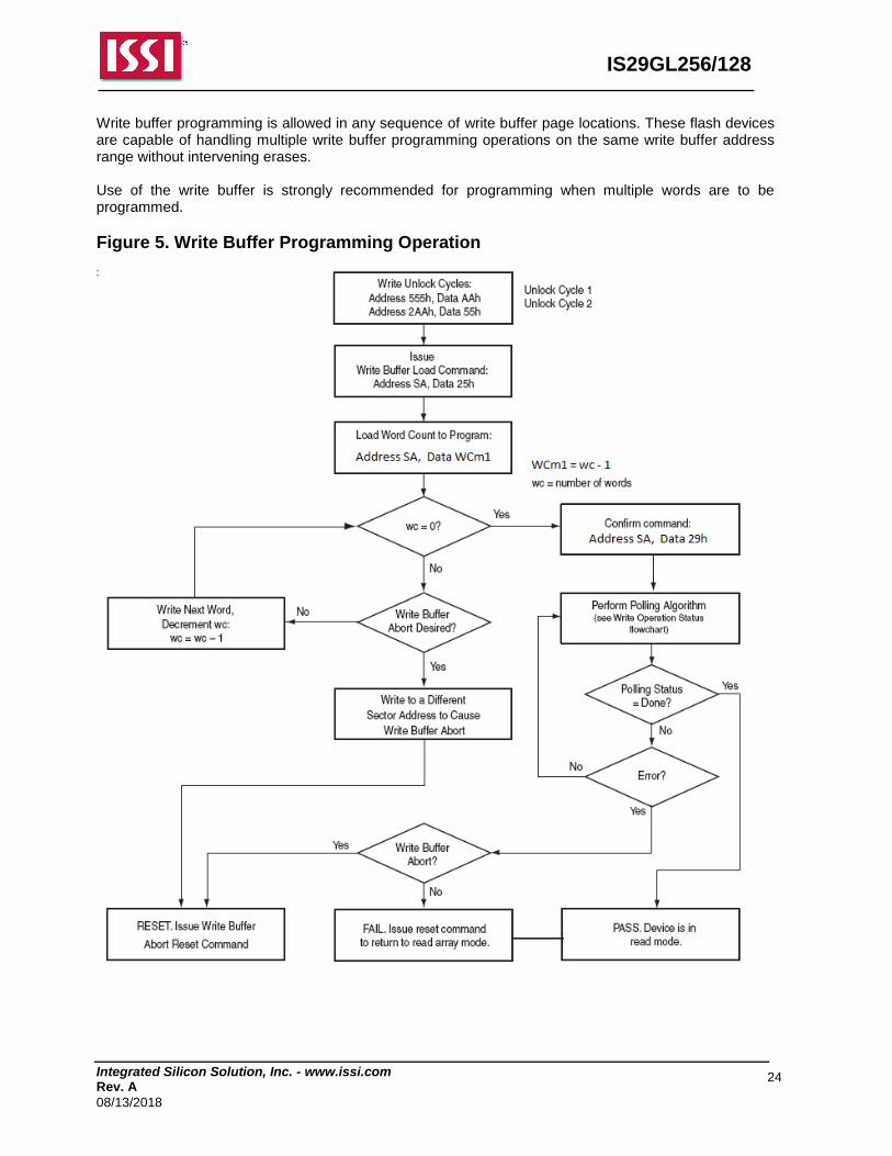
Sector Erase Sector erase is a six bus cycle operation. The sector erase command sequence is initiated by writing two un-lock cycles, followed by a set-up command. Two additional unlock write cycles are then followed by the address of the sector to be erased, with the sector erase command. The Command Definitions table shows the address and data requirements for the sector erase command sequence. Once the sector erase operation has begun, only Suspend command (B0h) is valid. All other commands are ignored. If there are several sectors to be erased, Sector Erase Command sequences must be issued for each sector. That is, only one sector address can be specified for each Sector Erase command. Users must issue another Sector Erase command for the next sector to be erased after the previous one is completed. When the Embedded Erase algorithm is completed, the device returns to reading array data and addresses are no longer latched. The system can determine the status of the erase operation by using DQ7, DQ6, or DQ2. Refer to “Write Operation Status” for information on these status bits. Flowchart on Figure 6 illustrates the algorithm for the erase operation. Refer to the Erase/Program Operations tables in the “AC Characteristics” section for parameters, and to the Sector Erase Operations Timing diagram for timing waveforms.
Figure 6. Sector Erase Operation
START
Write Erase Command Sequence
Data Poll from System or Toggle Bit
successfully completed
Erase Done
Data =FFh?
Yes
No
Integrated Silicon Solution, Inc. - www.issi.com Rev. A
08/13/2018
26
IS29GL256/128
Chip Erase Command Sequence Chip erase is a six-bus cycle operation as indicated by Table 13. These commands invoke the Embedded Erase algorithm, which does not require the system to preprogram prior to erase. The Embedded Erase algorithm automatically preprograms and verifies the entire memory to an all zero data pattern prior to electrical erase. After a successful chip erase, all locations of the chip contain FFFFh, except for any protected sectors. The system is not required to provide any controls or timings during these operations. When the Embedded Erase algorithm is complete, that sector returns to the read mode and addresses are no longer latched. The system can determine the status of the erase operation by using DQ7 or DQ6/DQ2. Refer to “Write Operation Status” for information on these status bits. Any commands including suspend command written during the chip erase operation are ignored. However, note that a hardware reset immediately terminates the erase operation. If that occurs, the chip erase command sequence should be reinitiated once that sector has returned to reading array data, to ensure the entire array is properly erased.
Erase Suspend/Erase Resume Sequence The Suspend command (B0h) allows the system to interrupt a sector erase operation and then read data from, or program data to, any sector not selected for erase. The Suspend command is ignored if written during the chip erase operation. Addresses are don’t-cares when writing the Suspend command during sector erase operation. When the Suspend command is written during the sector erase operation, the device requires a maximum of 20 µs to suspend the erase operation. After the sector erase operation has been suspended, the device enters the erase-suspend-read mode. The system can read data from or program data to any sector not selected for erasure. (The device “erase suspends” all sectors selected for erasure.) Reading at any address within erase-suspended sectors produces status information on DQ7-DQ0. The system can use DQ7, or DQ6, and DQ2 together, to determine if a sector is actively erasing or is erase-suspended. After an erase-suspended program operation is complete, the device returns to the erase-suspend-read mode. The system can determine the status of the program operation using write operation status bits, just as in the standard program operation. In the erase-suspend-read mode, the system can also issue Programing commands, the Autoselect command sequence, the Secured Silicon Region command, and CFI query command. Refer to Write Buffer Programming and the Autoselect for details. To resume the sector erase operation, the system must write the Resume command (30h). Further writes of the Resume command are ignored. Another Suspend command can be written after the chip has resumed sector erasing
Integrated Silicon Solution, Inc. - www.issi.com Rev. A
08/13/2018
27
IS29GL256/128
Program Suspend/Program Resume Sequence The Suspend command (B0h) also allows the system to interrupt an embedded programming operation or a “Write to Buffer” programming operation so that data can read from any non-suspended sector. When the Program Suspend command is written during a programming process, the device halts the programming operation within 15 µs maximum (5 µs typical) and updates the status bits. Addresses are “don't-cares” when writing the Suspend command. After the programming operation has been suspended, the system can read array data from any non-suspended sector. The Suspend command may also be issued during a programming operation while an erase is suspended. In this case, data may be read from any addresses not within a sector in Erase Suspend or Program Suspend. If a read is needed from the Secured Silicon Region, then user must use the proper command sequences to enter and exit this region. The system may also write the Autoselect Command Sequence and CFI query command when the device is in Program Suspend mode. The device allows reading Autoselect codes in the suspended sectors, since the codes are not stored in the memory array. When the device exits the Autoselect mode, the device reverts to Program Suspend mode, and is ready for another valid operation. After the Program Resume command is written, the device reverts to programming. The system can determine the status of the program operation using the write operation status bits, just as in the standard program operation. The system must write the Resume command (30h) to exit the Program Suspend mode (address bits are “don't care”) and continue the programming operation. Further writes of the Resume command are ignored. Another Suspend command can be written after the device has resumed programming.
Accelerated Program Accelerated single word programming and write buffer programming operations are enabled through the WP#/ACC pin. This method is faster than the standard program command sequences. If the system asserts VHH on this input, the device automatically enters the Accelerated Program mode and uses the higher voltage and current provided by WP#/ACC pin to reduce the time required for program operations. The system can then use the Write Buffer Load command sequence provided by the Accelerated Program mode. Note that if a “Write-to-Buffer-Abort Reset” is required while in Accelerated Program mode, the full 3-cycle RESET command sequence must be used to reset the device. Removing VHH from the ACC input, upon completion of the embedded program operation, returns the device to normal operation.
Sectors must be unlocked prior to raising WP#/ACC to VHH.
The WP#/ACC pin must not be at VHH for operations other than accelerated programming, or device damage may result.
It is recommended that WP#/ACC apply VHH after power-up sequence is completed. In addition, it is recommended that WP#/ACC apply from VHH to VIH/VIL before powering down VCC/ VIO.
Integrated Silicon Solution, Inc. - www.issi.com Rev. A
08/13/2018
28
IS29GL256/128
Write Operation Status The device provides several bits to determine the status of a program or erase operation. The following subsections describe the function of DQ1, DQ2, DQ3, DQ5, DQ6, and DQ7.
DQ7: Data# Polling The Data# Polling bit, DQ7, indicates to the host system whether an Embedded Program or Erase algorithm is in progress or completed, or whether the device is in Erase Suspend. Data# Polling is valid after the rising edge of the final WE# pulse in the command sequence. Note that the Data# Polling is valid only for the last word being programmed in the write-buffer-page during Write Buffer Programming. Reading Data# Polling status on any word other than the last word to be programmed in the write-buffer-page returns false status information. During the Embedded Program algorithm, the device outputs on DQ7 the complement of the datum programmed to DQ7. This DQ7 status also applies to programming during Erase Suspend. When the Embedded Program algorithm is complete, the device outputs the datum programmed to DQ7. The system must provide the program address to read valid status information on DQ7. If a program address falls within a protected sector, Data# polling on DQ7 is active, then that sector returns to the read mode, without changing any data. During the Embedded Erase Algorithm, Data# polling produces a “0” on DQ7. When the Embedded Erase algorithm is complete, or if the device enters the Erase Suspend mode, Data# Polling produces a “1” on DQ7. The system must provide an address within any of the sectors selected for erasure to read valid status information on DQ7. After a sector erase command sequence is written, if a sector selected for erasing are protected, Data# Polling on DQ7 is active for approximately 1µs (~256µs for chip erase when all sectors are protected), then the device returns to the read mode. For a chip erase command, if not all selected sectors are protected, the Embedded Erase algorithm erases the unprotected sectors, and ignores the selected sectors that are protected. However, if the system reads DQ7 at an address within a protected sector, the status may not be valid. Just prior to the completion of an Embedded Program or Erase operation, DQ7 may change asynchronously with DQ6-DQ0 while Output Enable (OE#) is asserted low. That is, the device may change from providing status information to valid data on DQ7. Depending on when the system samples the DQ7 output, it may read the status or valid data. Even if the device has completed the program or erase operation and DQ7 has valid data, the data outputs on DQ6-DQ0 may be still invalid. Valid data on DQ7-D00 appears on successive read cycles.
Integrated Silicon Solution, Inc. - www.issi.com Rev. A
08/13/2018
29
IS29GL256/128
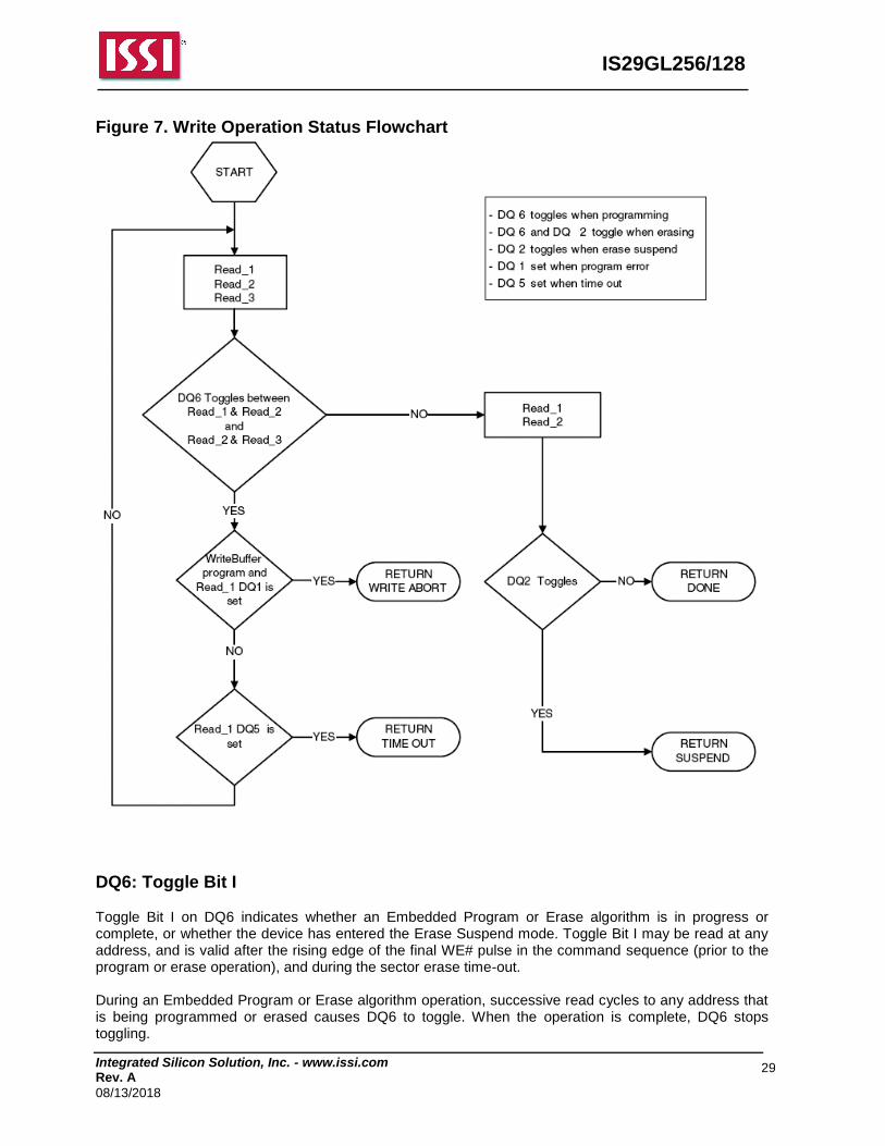
Figure 7. Write Operation Status Flowchart
DQ6: Toggle Bit I Toggle Bit I on DQ6 indicates whether an Embedded Program or Erase algorithm is in progress or complete, or whether the device has entered the Erase Suspend mode. Toggle Bit I may be read at any address, and is valid after the rising edge of the final WE# pulse in the command sequence (prior to the program or erase operation), and during the sector erase time-out. During an Embedded Program or Erase algorithm operation, successive read cycles to any address that is being programmed or erased causes DQ6 to toggle. When the operation is complete, DQ6 stops toggling.
Integrated Silicon Solution, Inc. - www.issi.com Rev. A
08/13/2018
30
IS29GL256/128
After a sector erase command sequence is written, if a sector selected for erasing are protected, DQ6 toggles for approximately 1 µs, then the device returns to the read mode. For a chip erase command, if not all sectors are protected, the Embedded Erase algorithm erases the unprotected sectors, and ignores the selected sectors that are protected. The system can use DQ6 and DQ2 together to determine whether a sector is actively erasing or is erase suspended. When the device is actively erasing (that is, the Embedded Erase algorithm is in progress), DQ6 toggles. When the device enters the Erase Suspend mode, DQ6 stops toggling. However, the system must also use DQ2 to determine which sectors are erasing or erase-suspended. Alternatively, the system can use DQ7. If a program address falls within a protected sector, DQ6 toggles for approximately 1μs after the program command sequence is written, then returns to reading array data. DQ6 also toggles during the erase-suspend-program mode, and stops toggling once the Embedded Program Algorithm is complete. Toggle Bit I on DQ6 requires either OE# or CE# to be de-asserted and reasserted to show the change in state.
DQ2: Toggle Bit II The “Toggle Bit II” on DQ2, when used with DQ6, indicates whether a particular sector is actively erasing (that is, the Embedded Erase algorithm is in progress), or whether that sector is erase-suspended. Toggle Bit II is valid after the rising edge of the final WE# pulse in the command sequence. DQ2 toggles when the system reads at addresses within those sectors that have been selected for erasure. But DQ2 cannot distinguish whether the sector is actively erasing or is erase-suspended. DQ6, by comparison, indicates whether the device is actively erasing, or is in Erase Suspend, but cannot distinguish which sectors are selected for erasure. Thus, both status bits are required for sector and mode information.
Reading Toggle Bits DQ6/DQ2
Whenever the system initially begins reading toggle bit status, it must read DQ7–DQ0 at least twice in a row to determine whether a toggle bit is toggling. Typically, the system would note and store the value of the toggle bit after the first read. After the second read, the system would compare the new value of the toggle bit with the first. If the toggle bit is not toggling, the device has completed the program or erases operation. The system can read array data on DQ7–DQ0 on the following read cycle. However, if after the initial two read cycles, the system determines that the toggle bit is still toggling, the system also should note whether the value of DQ5 is high. If it is, the system should then determine again whether the toggle bit is toggling, since the toggle bit may have stopped toggling just as DQ5 went high. If the toggle bit is no longer toggling, the device has successfully completed the program or erases operation. If it is still toggling, the device did not complete the operation successfully, and the system must write the reset command to return to reading array data. The remaining scenario is that the system initially determines that the toggle bit is toggling and DQ5 has not gone high. The system may continue to monitor the toggle bit and DQ5 through successive read cycles, determining the status as described in the previous paragraph. Alternatively, it may choose to perform other system tasks. In this case, the system must start at the beginning of the algorithm when it returns to determine the status of the operation.
Note When verifying the status of a write operation (embedded program/erase) of a memory sector, DQ6 and DQ2 toggle between high and low states in a series of consecutive and contiguous status read cycles. In order for this toggling behavior to be properly observed, the consecutive status bit reads must not be interleaved with read accesses to other memory sectors. If it is not possible to temporarily prevent reads to other memory sectors, then it is recommended to use the DQ7 status bit as the alternative method of determining the active or inactive status of the write operation.
Integrated Silicon Solution, Inc. - www.issi.com Rev. A
08/13/2018
31
IS29GL256/128
DQ5: Exceeded Timing Limits DQ5 indicates whether the program or erase time has exceeded a specified internal pulse count limit. Under these conditions DQ5 produces a “1,” indicating that the program or erase cycle was not successfully completed. The device does not output a 1 on DQ5 if the system tries to program a 1 to a location that was previously programmed to 0. Only an erase operation can change a 0 back to a 1. Under this condition, the device ignores the bit that was incorrectly instructed to be programmed from a 0 to a 1, while any other bits that were correctly requested to be changed from 1 to 0 are programmed. Attempting to program a 0 to a 1 is masked during the programming operation. Under valid DQ5 conditions, the system must write the reset command to return to the read mode (or to the erase-suspend-read mode if a sector was previously in the erase-suspend-program mode).
DQ3: Sector Erase Timeout State Indicator After writing a sector erase command sequence, the output on DQ3 can be checked to determine whether or not an erase operation has begun. (The sector erase timer does not apply to the chip erase command.) When sector erase starts, DQ3 switches from “0” to “1”. This device does not support multiple sector erase (continuous sector erase) command sequences so it is not very meaningful since it immediately shows as a “1” after the first 30h command. Future devices may support this feature.
DQ1: Write to Buffer Abort DQ1 indicates whether a Write to Buffer operation was aborted. Under these conditions DQ1 produces a “1”. The system must issue the “Write to Buffer Abort Reset” command sequence to return the device to reading array data.
Table 5. Write Operation Status
Status DQ7
(note 2) DQ6
DQ5 (note 1)
DQ3 DQ2
(note 2) DQ1 RY/BY#
Standard Mode
Embedded Program Algorithm DQ7# Toggle 0 N/A No
Toggle 0 0
Embedded Erase Algorithm 0 Toggle 0 1 Toggle N/A 0
Program Suspend
Mode
Program Suspend
Read
Program Suspended Sector
Invalid (Not allowed) 1
Non-Program Suspended Sector
Data 1
Erase Suspend
Mode
Erase Suspend
Read
Erase Suspended Sector
1 No
Toggle 0 N/A Toggle N/A 1
Non-Erase Suspended Sector
Data 1
Erase Suspend Program (Embedded Program)
DQ7# Toggle 0 N/A N/A N/A 0
Write to Buffer
Busy(note 3) DQ7# Toggle 0 N/A N/A 0 0
Abort(note 4) DQ7# Toggle 0 N/A N/A 1 0
Notes 1. DQ5 switches to 1 when an Embedded Program, Embedded Erase, or Write-to-Buffer operation has
exceeded the maximum timing limits. 2. DQ7 and DQ2 require a valid address when reading status information. Refer to the appropriate subsection for further details. 3. The Data# Polling algorithm should be used to monitor the last loaded write-buffer address location. 4. DQ1 switches to 1 when the device has aborted the write-to-buffer operation
Integrated Silicon Solution, Inc. - www.issi.com Rev. A
08/13/2018
32
IS29GL256/128
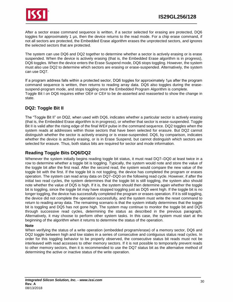
Figure 8. Data Polling Flowchart
Read DQ7, DQ5, and DQ1
at valid address
Read DQ7 at valid address
DQ7 = Data
DQ5 = 1
DQ7 = Data
DQ1 = 1
YES
YES
NO
YES
NO
NO
Start
Failure Success
(1)
(2)(3)
YES
Notes: 1. Valid address is the address being programmed or an address within the block being erased. 2. Failure results: DQ5 = 1 indicates an operation error. 3. DQ1 = 1 indicates a WRITE TO BUFFER PROGRAM ABORT operation.
Integrated Silicon Solution, Inc. - www.issi.com Rev. A
08/13/2018
33
IS29GL256/128
Writing Commands/Command Sequences During a write operation, the system must drive CE# and WE# to VIL and OE# to VIH when providing an address, command, and data. Addresses are latched on the last falling edge of WE# or CE#, whichever is last, while data is latched on the 1st rising edge of WE# or CE#, whichever is first. An erase operation can erase one sector or the entire device. Table 3 indicates the address space that each sector occupies. The device address space is divided into uniform 64KW/128KB sectors. A sector address is the set of address bits required to uniquely select a sector. ICC2 in “DC Characteristics” represents the active current specification for the write mode. “AC Characteristics” contains timing specification tables and timing diagrams for write operations.
RY/BY# The RY/BY# is a dedicated, open-drain output pin that indicates whether an Embedded Algorithm is in progress or complete. The RY/BY# status is valid after the rising edge of the final WE# pulse in the command sequence. Since RY/BY# is an open-drain output, several RY/BY# pins can be tied together in parallel with a pull-up resistor to VCC. This feature allows the host system to detect when data is ready to be read by simply monitoring the RY/BY# pin, which is a dedicated output and controlled by CE# (not OE#).
Hardware Reset The RESET# input provides a hardware method of resetting the device to reading array data. When RESET# is driven low for at least a period of tRP (RESET# Pulse Width), the device immediately terminates any operation in progress, tri-states all outputs, resets the configuration register, and ignores all read/write commands for the duration of the RESET# pulse. The device also resets the internal state machine to reading array data. To ensure data integrity Program/Erase operations that were interrupted should be reinitiated once the device is ready to accept another command sequence. When RESET# is held at VSS, the device draws VCC reset current (ICC5). If RESET# is held at VIL, but not at VSS, the standby current is greater. RESET# may be tied to the system reset circuitry which enables the system to read the boot-up firmware from the Flash memory upon a system reset.
Integrated Silicon Solution, Inc. - www.issi.com Rev. A
08/13/2018
34
IS29GL256/128
Software Reset Software reset is part of the command set that also returns the device to array read mode and must be used for the following conditions: 1. To exit from Autoselect or CFI mode back to read mode. It returns back to erase-suspend-read mode if
the device was previously in Erase Suspend mode. 2. When DQ5 goes high during write status operation that indicates program or erase cycle was not
successfully completed 3. Exit sector lock/unlock operation. 4. After any aborted operations The following are additional points to consider when using the reset command:
This command resets the device to read mode and address bits are ignored.
Reset commands are ignored during program and erase operations.
The reset command may be written between the cycles in a program command sequence before programming begins (prior to the third cycle). This resets the sector to which the system was writing to the read mode.
If the program command sequence is written to a sector that is in the Erase Suspend mode, writing the reset command returns that sector to the erase-suspend-read mode.
The reset command may be written during an Autoselect command sequence.
If a sector has entered the Autoselect mode while in the Erase Suspend mode, writing the reset command returns that sector to the erase-suspend-read mode.
If DQ1 goes high during a Write Buffer Programming operation, the system must write the “Write to Buffer Abort Reset” command sequence to RESET the device to reading array data. The standard RESET command does not work during this condition.
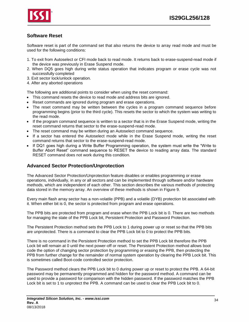
Advanced Sector Protection/Unprotection The Advanced Sector Protection/Unprotection feature disables or enables programming or erase operations, individually, in any or all sectors and can be implemented through software and/or hardware methods, which are independent of each other. This section describes the various methods of protecting data stored in the memory array. An overview of these methods is shown in Figure 9. Every main flash array sector has a non-volatile (PPB) and a volatile (DYB) protection bit associated with it. When either bit is 0, the sector is protected from program and erase operations. The PPB bits are protected from program and erase when the PPB Lock bit is 0. There are two methods for managing the state of the PPB Lock bit, Persistent Protection and Password Protection. The Persistent Protection method sets the PPB Lock to 1 during power up or reset so that the PPB bits are unprotected. There is a command to clear the PPB Lock bit to 0 to protect the PPB bits. There is no command in the Persistent Protection method to set the PPB Lock bit therefore the PPB Lock bit will remain at 0 until the next power-off or reset. The Persistent Protection method allows boot code the option of changing sector protection by programming or erasing the PPB, then protecting the PPB from further change for the remainder of normal system operation by clearing the PPB Lock bit. This is sometimes called Boot-code controlled sector protection. The Password method clears the PPB Lock bit to 0 during power up or reset to protect the PPB. A 64-bit password may be permanently programmed and hidden for the password method. A command can be used to provide a password for comparison with the hidden password. If the password matches the PPB Lock bit is set to 1 to unprotect the PPB. A command can be used to clear the PPB Lock bit to 0.
Integrated Silicon Solution, Inc. - www.issi.com Rev. A
08/13/2018
35
IS29GL256/128
1. 0 = PPBs Locked, 1 = PPBs Unlocked
2. Bit is volatile, and defaults to “1” on reset.
3. Programming to “0” locks all PPBs to their current state. 4. Once programmed to “0”, requires hardware reset to
unlock
Persistent Protection Bit (PPB)
Sector 0 DYB 0 PPB Lock Bit PPB 0
Sector 1 DYB 1 PPB 1 1
Sector 2 PPB 2 2
DYB 2
DYB 3 Sector 3 PPB 3
Sector 252
Sector 253
Sector 254
DYB 252
DYB 253
DYB 254
Sector 255
DYB 255
PPB 252
PPB 255
PPB 253
PPB 254
Figure 9. Advanced Sector Protection/Unprotection
5. 0 = Sector Protected
1 = Sector Unprotected
6. DYB bits are only effective for
sectors that are not protected
via PPB (PPB = 1).
7. Volatile Bits: defaults to unprotected after power up.
8. 0 = Sector Protected
1 = Sector Unprotected
9. PPBs programmed to 0
individually, but erased to 1
collectively.
The selection of the PPB Lock management method is made by programming OTP bits in the Lock Register so as to permanently select the method used. The Lock Register also contains OTP bits, for protecting the Secured Silicon Region. The PPB bits are erased so that all main flash array sectors are unprotected when shipped from factory. The Factory Locked Secured Silicon Region is always factory locked when shipped from the factory.
Dynamic Protection Bit (DYB)
Memory Array
Password Protection Mode (DQ2)
Lock Register Bits (OTP)
Persistent Protection Mode (DQ1)
64-bit Password (OTP)
Integrated Silicon Solution, Inc. - www.issi.com Rev. A
08/13/2018
36
IS29GL256/128
Lock Register The Lock Register consists of 16 bits and each of these bits in the lock register are non-volatile OTP. The Factory Locked Secured Silicon Region Lock Bit is DQ0 and The Customer Locked Secured Silicon Region Lock Bit is DQ6. DQ0 is always ‘0’, and it means that the Factory Secured Silicon Region is always locked when shipped from the factory. If DQ6 is ‘0’, it means that the Customer Locked Secured Silicon Region is locked and if DQ6 is ‘1’, it means that it is unlocked. The Customer Locked Secure Silicon Region Lock Bit must be used with caution, as once locked, there is no procedure available for unlocking the protected portion of the Secure Silicon Region and none of the bits in the protected Secure Silicon Region memory space can be modified in any way. Once Customer Locked Secure Silicon Region area is locked, any further attempts to program in the area will fail. The Persistent Protection Mode Lock Bit is DQ1 and the Password Protection Mode Lock Bit is DQ2. If DQ1 is set to ‘0’, the device is used in the Persistent Protection Mode. If DQ2 is set to ‘0’, the device is used in the Password Protection Mode. When shipped from the factory, all devices default to the Persistent Protection method. Either DQ1 or DQ2 can be programmed by user. Once programming one of them another one will be permanently disabled and any change is not allowed. If both DQ1 and DQ2 are selected to be programmed at the same time, the operation will abort.
PPB Protection OTP bit is DQ3 and DYB Lock Boot Bit is DQ4. DQ3 is programmed in the ISSI factory. When the device is programmed to disable all PPB erase command, DQ3 outputs a ‘0’ when the lock register bits are read. Similarly, if the device is programmed to enable all PPB erase command, DQ3 outputs a ‘1’ when the lock register bits are read. Likewise the DQ4 bit is also programmed in the ISSI Factory. DQ4 is the bit which indicates whether Volatile Sector Protection Bit (DYB) is protected or not after boot-up. When the device is programmed to set all Volatile Sector Protection Bit protected after power-up, DQ4 outputs a ‘0’ when the lock register bits are read. Similarly, when the device is programmed to set all Volatile Sector Protection Bit unprotected after power-up, DQ4 outputs a ‘1’. DQ5 and DQ15 ~ DQ7 are reserved and will be 1’s.
Table 6. Lock Register Bit Default Description
DQ15 ~ DQ7 Each Bit = 1 Reserved
DQ6 1 Customer Locked Secured Silicon Region Lock Bit (0 = locked, 1 = unlocked)
DQ5 1 Reserved
DQ4 1
DYB Lock Boot Bit 0 = protected all DYB after boot-up 1 = unprotected all DYB after boot-up
DQ3 1
PPB One Time Programmable Bit 0 = All PPB Erase Command disabled 1 = All PPB Erase Command enabled
DQ2 1 Password Protection Mode Lock Bit
DQ1 1 Persistent Protection Mode Lock Bit
DQ0 0 Factory Locked Secured Silicon Region Lock Bit (0 = locked, always locked from factory)
Notes: 1. If the password mode is chosen, the password must be programmed before setting the corresponding lock register bit. 2. After the Lock Register Bits Command Set Entry command sequence is written, reads and writes for Sector 0 are disabled, while
reads from other sectors are allowed until exiting this mode. 3. After selecting a sector protection method, each sector can operate in any of the following three states: - Constantly locked: The selected sectors are protected and cannot be reprogrammed unless PPB lock bit is cleared via hardware reset, or power cycle. - Dynamically locked: The selected sectors are protected but can be unprotected via software commands. - Unlocked: The sectors are unprotected and can be erased and/or programmed.
Integrated Silicon Solution, Inc. - www.issi.com Rev. A
08/13/2018
37
IS29GL256/128
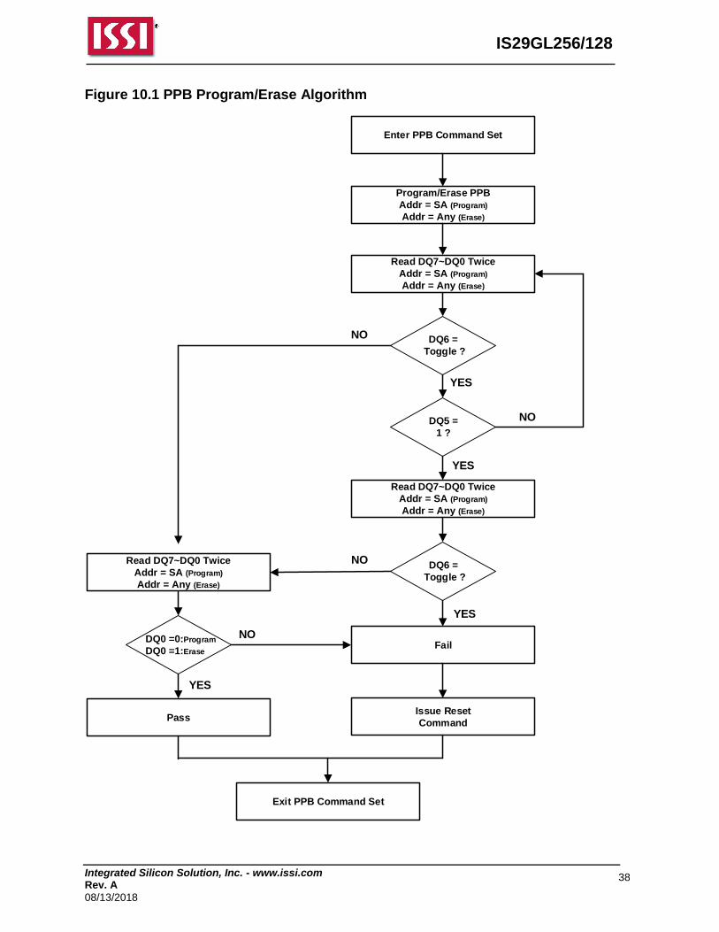
Persistent Protection Bits
The Persistent Protection Bits are unique for each sector and nonvolatile (refer to Figure 9 and Table 3. Sector / Persistent Protection Sector Group Address Tables). It has the same endurances as the Flash memory. Preprogramming and verification prior to erasure are handled by the device, and therefore do not require system monitoring. There is a command to clear the PPB Lock bit to 0 to protect the PPB. However, there is no command in the Persistent Protection method to set the PPB Lock bit to 1 therefore the PPB Lock bit will remain at 0 until the next power up or reset. Notes 1. Each PPB is individually programmed and all are erased in parallel. 2. While programming PPB and data polling on programming PPB address, array data cannot be read
from any sectors. 3. Entry command disables reads and writes for all sectors. 4. Reads within that sector return the PPB status for that sector. 5. If the PPB Lock Bit is set, the PPB Program or erase command does not execute and times-out without programming or erasing the PPB. 6. There are no means for individually erasing a specific PPB and no specific sector address is required for
this operation. 7. Exit command must be issued after the execution which resets the device to read mode and re-enables
reads and writes for all sectors. 8. The programming state of the PPB for given sectors can be verified by writing a PPB Status Read
Command to the device as described by the flow chart shown in Figure 10.1. User only can use DQ6 and RY/BY# pin to detect programming status.
Integrated Silicon Solution, Inc. - www.issi.com Rev. A
08/13/2018
38
IS29GL256/128
Figure 10.1 PPB Program/Erase Algorithm
Enter PPB Command Set
Program/Erase PPB
Addr = SA (Program)
Addr = Any (Erase)
Read DQ7~DQ0 Twice
Addr = SA (Program)
Addr = Any (Erase)
Read DQ7~DQ0 Twice
Addr = SA (Program)
Addr = Any (Erase)
Fail
Read DQ7~DQ0 Twice
Addr = SA (Program)
Addr = Any (Erase)
Pass
DQ6 =
Toggle ?
DQ5 =
1 ?
DQ6 =
Toggle ?
DQ0 =0:Program
DQ0 =1:Erase
Issue Reset
Command
Exit PPB Command Set
NO
NO
YES
NO
YES
YES
YES
NO
Integrated Silicon Solution, Inc. - www.issi.com Rev. A
08/13/2018
39
IS29GL256/128
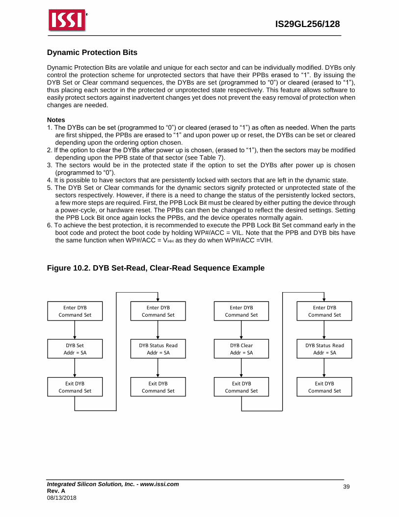
Dynamic Protection Bits
Dynamic Protection Bits are volatile and unique for each sector and can be individually modified. DYBs only control the protection scheme for unprotected sectors that have their PPBs erased to “1”. By issuing the DYB Set or Clear command sequences, the DYBs are set (programmed to “0”) or cleared (erased to “1”), thus placing each sector in the protected or unprotected state respectively. This feature allows software to easily protect sectors against inadvertent changes yet does not prevent the easy removal of protection when changes are needed. Notes 1. The DYBs can be set (programmed to “0”) or cleared (erased to “1”) as often as needed. When the parts
are first shipped, the PPBs are erased to “1” and upon power up or reset, the DYBs can be set or cleared depending upon the ordering option chosen.
2. If the option to clear the DYBs after power up is chosen, (erased to “1”), then the sectors may be modified depending upon the PPB state of that sector (see Table 7).
3. The sectors would be in the protected state if the option to set the DYBs after power up is chosen (programmed to “0”).
4. It is possible to have sectors that are persistently locked with sectors that are left in the dynamic state. 5. The DYB Set or Clear commands for the dynamic sectors signify protected or unprotected state of the
sectors respectively. However, if there is a need to change the status of the persistently locked sectors, a few more steps are required. First, the PPB Lock Bit must be cleared by either putting the device through a power-cycle, or hardware reset. The PPBs can then be changed to reflect the desired settings. Setting the PPB Lock Bit once again locks the PPBs, and the device operates normally again.
6. To achieve the best protection, it is recommended to execute the PPB Lock Bit Set command early in the boot code and protect the boot code by holding WP#/ACC = VIL. Note that the PPB and DYB bits have the same function when WP#/ACC = VHH as they do when WP#/ACC =VIH.
Figure 10.2. DYB Set-Read, Clear-Read Sequence Example
Enter DYB
Command Set
DYB Set
Addr = SA
Exit DYB
Command Set
Enter DYB
Command Set
DYB Status Read
Addr = SA
Exit DYB
Command Set
Enter DYB
Command Set
DYB Clear
Addr = SA
Exit DYB
Command Set
Enter DYB
Command Set
DYB Status Read
Addr = SA
Exit DYB
Command Set
Integrated Silicon Solution, Inc. - www.issi.com Rev. A
08/13/2018
40
IS29GL256/128
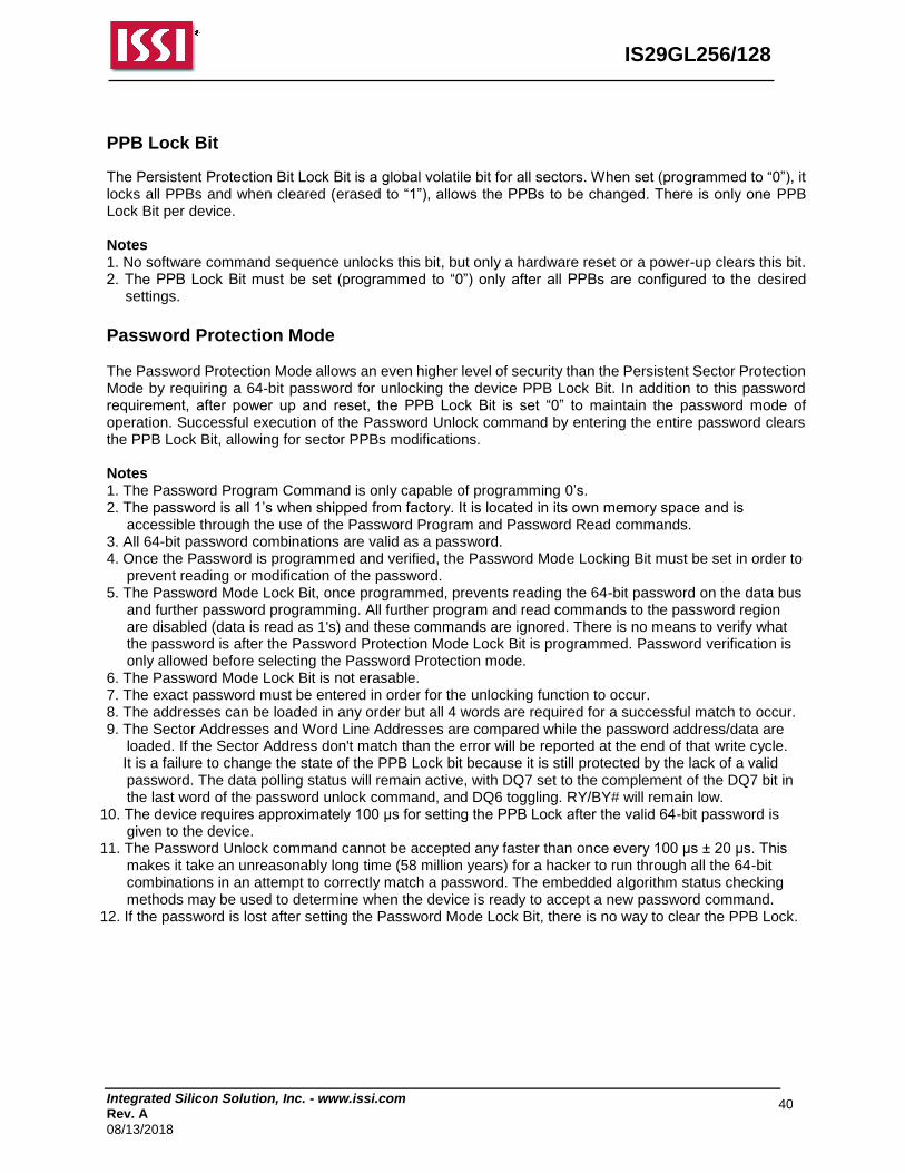
PPB Lock Bit
The Persistent Protection Bit Lock Bit is a global volatile bit for all sectors. When set (programmed to “0”), it locks all PPBs and when cleared (erased to “1”), allows the PPBs to be changed. There is only one PPB Lock Bit per device. Notes 1. No software command sequence unlocks this bit, but only a hardware reset or a power-up clears this bit. 2. The PPB Lock Bit must be set (programmed to “0”) only after all PPBs are configured to the desired
settings.
Password Protection Mode The Password Protection Mode allows an even higher level of security than the Persistent Sector Protection Mode by requiring a 64-bit password for unlocking the device PPB Lock Bit. In addition to this password requirement, after power up and reset, the PPB Lock Bit is set “0” to maintain the password mode of operation. Successful execution of the Password Unlock command by entering the entire password clears the PPB Lock Bit, allowing for sector PPBs modifications. Notes 1. The Password Program Command is only capable of programming 0’s. 2. The password is all 1’s when shipped from factory. It is located in its own memory space and is
accessible through the use of the Password Program and Password Read commands. 3. All 64-bit password combinations are valid as a password. 4. Once the Password is programmed and verified, the Password Mode Locking Bit must be set in order to
prevent reading or modification of the password. 5. The Password Mode Lock Bit, once programmed, prevents reading the 64-bit password on the data bus
and further password programming. All further program and read commands to the password region are disabled (data is read as 1's) and these commands are ignored. There is no means to verify what the password is after the Password Protection Mode Lock Bit is programmed. Password verification is only allowed before selecting the Password Protection mode.
6. The Password Mode Lock Bit is not erasable. 7. The exact password must be entered in order for the unlocking function to occur. 8. The addresses can be loaded in any order but all 4 words are required for a successful match to occur. 9. The Sector Addresses and Word Line Addresses are compared while the password address/data are
loaded. If the Sector Address don't match than the error will be reported at the end of that write cycle. It is a failure to change the state of the PPB Lock bit because it is still protected by the lack of a valid
password. The data polling status will remain active, with DQ7 set to the complement of the DQ7 bit in the last word of the password unlock command, and DQ6 toggling. RY/BY# will remain low.
10. The device requires approximately 100 μs for setting the PPB Lock after the valid 64-bit password is given to the device.
11. The Password Unlock command cannot be accepted any faster than once every 100 μs ± 20 μs. This makes it take an unreasonably long time (58 million years) for a hacker to run through all the 64-bit combinations in an attempt to correctly match a password. The embedded algorithm status checking methods may be used to determine when the device is ready to accept a new password command.
12. If the password is lost after setting the Password Mode Lock Bit, there is no way to clear the PPB Lock.
Integrated Silicon Solution, Inc. - www.issi.com Rev. A
08/13/2018
41
IS29GL256/128
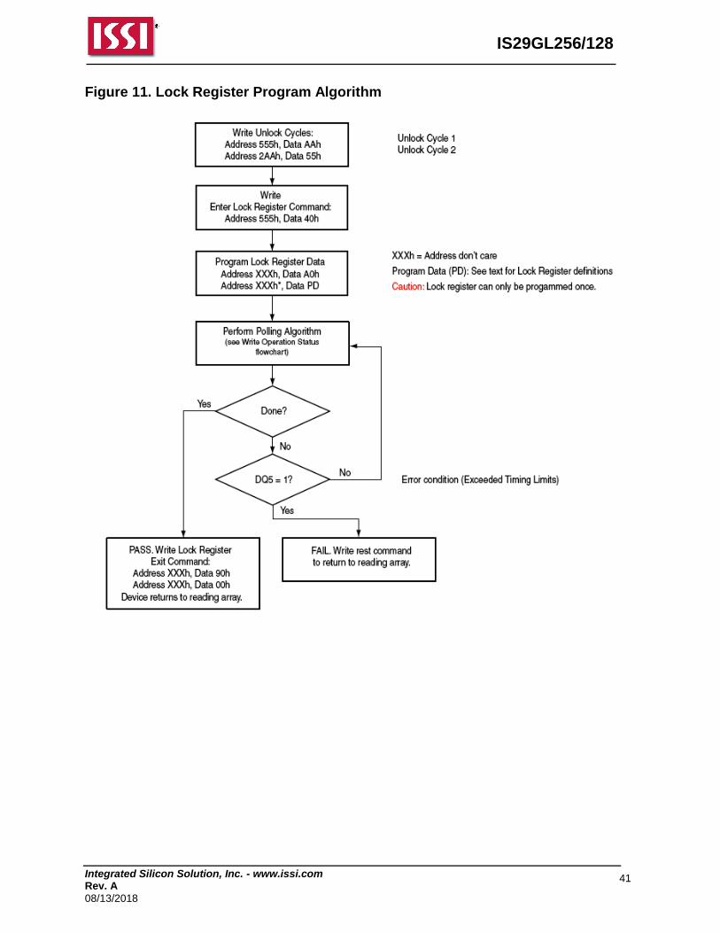
Figure 11. Lock Register Program Algorithm
Integrated Silicon Solution, Inc. - www.issi.com Rev. A
08/13/2018
42
IS29GL256/128
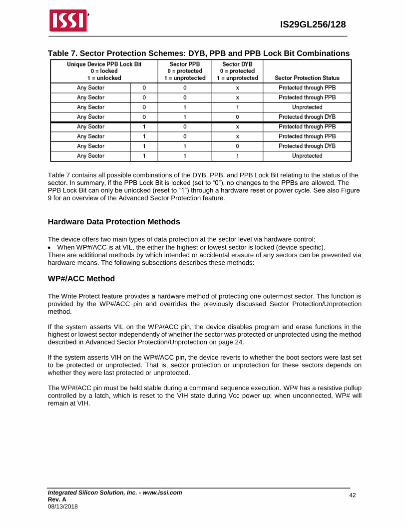
Table 7. Sector Protection Schemes: DYB, PPB and PPB Lock Bit Combinations
Table 7 contains all possible combinations of the DYB, PPB, and PPB Lock Bit relating to the status of the sector. In summary, if the PPB Lock Bit is locked (set to “0”), no changes to the PPBs are allowed. The PPB Lock Bit can only be unlocked (reset to “1”) through a hardware reset or power cycle. See also Figure 9 for an overview of the Advanced Sector Protection feature.
Hardware Data Protection Methods The device offers two main types of data protection at the sector level via hardware control:
When WP#/ACC is at VIL, the either the highest or lowest sector is locked (device specific). There are additional methods by which intended or accidental erasure of any sectors can be prevented via hardware means. The following subsections describes these methods:
WP#/ACC Method The Write Protect feature provides a hardware method of protecting one outermost sector. This function is provided by the WP#/ACC pin and overrides the previously discussed Sector Protection/Unprotection method. If the system asserts VIL on the WP#/ACC pin, the device disables program and erase functions in the highest or lowest sector independently of whether the sector was protected or unprotected using the method described in Advanced Sector Protection/Unprotection on page 24. If the system asserts VIH on the WP#/ACC pin, the device reverts to whether the boot sectors were last set to be protected or unprotected. That is, sector protection or unprotection for these sectors depends on whether they were last protected or unprotected. The WP#/ACC pin must be held stable during a command sequence execution. WP# has a resistive pullup controlled by a latch, which is reset to the VIH state during Vcc power up; when unconnected, WP# will remain at VIH.
Integrated Silicon Solution, Inc. - www.issi.com Rev. A
08/13/2018
43
IS29GL256/128
Low VCC Write Inhibit When VCC is less than VLKO (Lock-Out Voltage), the device does not accept any write cycles. This protects data during VCC power-up and power-down. The command register and all internal program/erase circuits are disabled, and the device resets to reading array data. Subsequent writes are ignored until VCC is greater than VLKO. The system must provide the proper signals to the control inputs to prevent unintentional writes when VCC is greater than VLKO.
Write Pulse “Glitch Protection” Noise pulses of less than 5 ns (typical) on OE#, CE# or WE# do not initiate a write cycle.
Power-Up Write Inhibit If WE# = CE# = RESET# = VIL and OE# = VIH during power up, the device does not accept commands on the rising edge of WE#. The internal state machine is automatically reset to the read mode on power-up.
Power Conservation Modes
Standby Mode When the system is not reading or writing to the device, it can place the device in the standby mode. In this mode, current consumption is greatly reduced, and the outputs are placed in the high impedance state, independent of the OE# input. The device enters the CMOS standby mode when the CE# and RESET# inputs are both held at VCC ± 0.3 V. The device requires standard access time (tCE) for read access, before it is ready to read data. If the device is deselected during erasure or programming, the device draws active current until the operation is completed. ICC4 in “DC Characteristics” represents the standby current specification
Automatic Sleep Mode The automatic sleep mode minimizes Flash device energy consumption. The device automatically enables this mode when addresses remain stable for tACC + 30 ns. The automatic sleep mode is independent of the CE#, WE#, and OE# control signals. Standard address access timings provide new data when addresses are changed. While in sleep mode, output data is latched and always available to the system.
Hardware RESET# Input Operation The RESET# input provides a hardware method of resetting the device to reading array data. When RESET# is driven low for at least a period of tRP, the device immediately terminates any operation in progress, tristates all outputs, and ignores all read/write commands for the duration of the RESET# pulse. The device also resets the internal state machine to reading array data. The operation that was interrupted should be reinitiated once the device is ready to accept another command sequence to ensure data integrity. When RESET# is held at VSS ± 0.3 V, the device draws ICC reset current (ICC5). If RESET# is held at VIL but not within VSS ± 0.3 V, the standby current is greater. RESET# may be tied to the system reset circuitry and thus, a system reset would also reset the Flash memory, enabling the system to read the boot-up firmware from the Flash memory.
Output Disable (OE#) When the OE# input is at VIH, output from the device is disabled. The outputs are placed in the high impedance state. (With the exception of RY/BY#.)
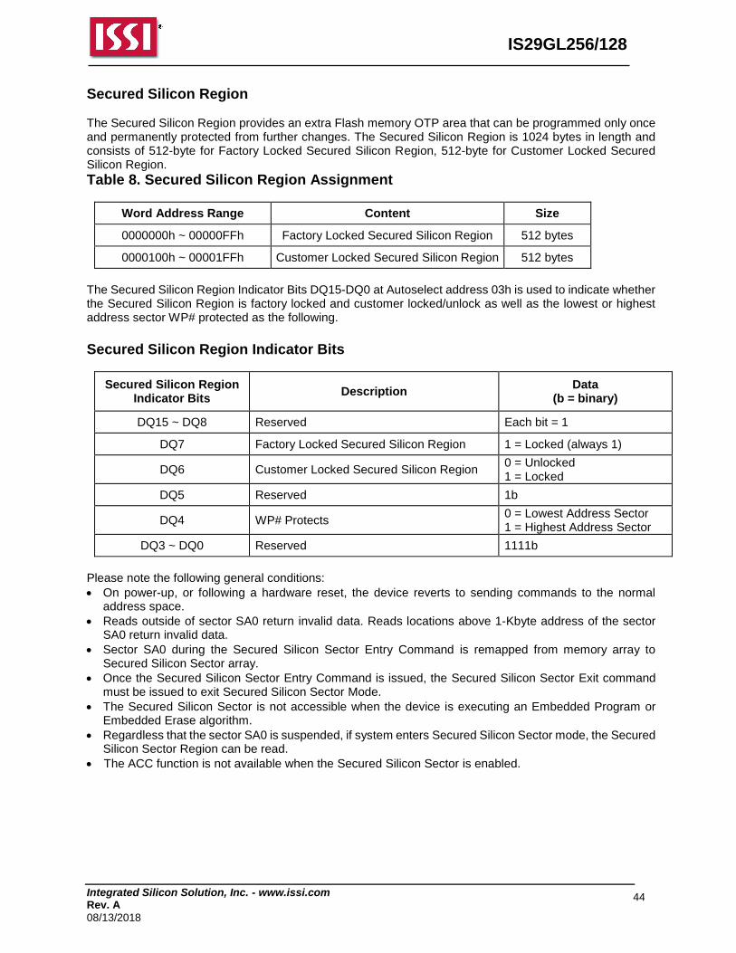
Integrated Silicon Solution, Inc. - www.issi.com Rev. A
08/13/2018
44
IS29GL256/128
Secured Silicon Region The Secured Silicon Region provides an extra Flash memory OTP area that can be programmed only once and permanently protected from further changes. The Secured Silicon Region is 1024 bytes in length and consists of 512-byte for Factory Locked Secured Silicon Region, 512-byte for Customer Locked Secured Silicon Region.
Table 8. Secured Silicon Region Assignment
Word Address Range Content Size
0000000h ~ 00000FFh Factory Locked Secured Silicon Region 512 bytes
0000100h ~ 00001FFh Customer Locked Secured Silicon Region 512 bytes
The Secured Silicon Region Indicator Bits DQ15-DQ0 at Autoselect address 03h is used to indicate whether the Secured Silicon Region is factory locked and customer locked/unlock as well as the lowest or highest address sector WP# protected as the following.
Secured Silicon Region Indicator Bits
Secured Silicon Region Indicator Bits
Description Data
(b = binary)
DQ15 ~ DQ8 Reserved Each bit = 1
DQ7 Factory Locked Secured Silicon Region 1 = Locked (always 1)
DQ6 Customer Locked Secured Silicon Region 0 = Unlocked 1 = Locked
DQ5 Reserved 1b
DQ4 WP# Protects 0 = Lowest Address Sector 1 = Highest Address Sector
DQ3 ~ DQ0 Reserved 1111b
Please note the following general conditions:
On power-up, or following a hardware reset, the device reverts to sending commands to the normal address space.
Reads outside of sector SA0 return invalid data. Reads locations above 1-Kbyte address of the sector SA0 return invalid data.
Sector SA0 during the Secured Silicon Sector Entry Command is remapped from memory array to Secured Silicon Sector array.
Once the Secured Silicon Sector Entry Command is issued, the Secured Silicon Sector Exit command must be issued to exit Secured Silicon Sector Mode.
The Secured Silicon Sector is not accessible when the device is executing an Embedded Program or Embedded Erase algorithm.
Regardless that the sector SA0 is suspended, if system enters Secured Silicon Sector mode, the Secured Silicon Sector Region can be read.
The ACC function is not available when the Secured Silicon Sector is enabled.
Integrated Silicon Solution, Inc. - www.issi.com Rev. A
08/13/2018
45
IS29GL256/128
Factory Locked Secured Silicon Region The Factory Locked Secured Silicon Region is always programmed and locked in the ISSI factory. Factory Locked Secured Silicon Region Indicator Bit DQ7 is always “1” and Factory Locked Secured Silicon Region Lock Bit DQ0 of the Lock Register is always “0” from the factory.
Customer Locked Secured Silicon Region The Customer Locked Secured Silicon Region is always unprotected when shipped from the factory (Customer Locked Secured Silicon Region Indicator Bit DQ6 set to “0”), allowing customers to utilize that sector in any manner they choose. Please note the following:
The Secured Silicon Region can be read any number of times, but can be programmed and locked only once. The Customer Locked Secured Silicon Region must be locked with caution, as once locked, there is no procedure available for unlocking the Customer Locked Secured Silicon Region and none of the bits in the Customer Locked Secured Silicon Sector memory space can be modified in any way.
The accelerated programming (ACC) is not available when the Secured Silicon Region is enabled.
Once the Secured Silicon Region is locked and verified, the system must write the Exit Secured Silicon Region command sequence which return the device to the memory array at sector 0.
Secured Silicon Region Entry/Exit Command Sequences The system can access the Secured Silicon Region by issuing the three-cycle Enter Secured Silicon Region command sequence. The device continues to access the Secured Silicon Region until the system issues the four-cycle Exit Secured Silicon Region command sequence. The Secured Silicon Region Entry Command allows the following commands to be executed
Read Customer Locked Secured Silicon Region and Factory Locked Secured Silicon Region
Program the Customer Locked Secured Silicon Region After the system has written the Enter Secured Silicon Region command sequence, it may read the Secured Silicon Region by using the addresses normally occupied by sector SA0 within the memory array. This mode of operation continues until the system issues the Exit Secured Silicon Region command sequence, or until power is removed from the device.
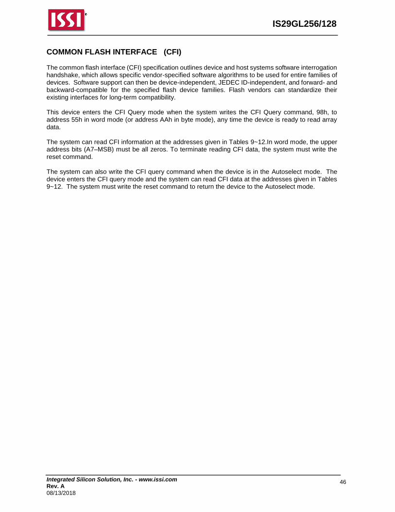
Integrated Silicon Solution, Inc. - www.issi.com Rev. A
08/13/2018
46
IS29GL256/128
COMMON FLASH INTERFACE (CFI) The common flash interface (CFI) specification outlines device and host systems software interrogation handshake, which allows specific vendor-specified software algorithms to be used for entire families of devices. Software support can then be device-independent, JEDEC ID-independent, and forward- and backward-compatible for the specified flash device families. Flash vendors can standardize their existing interfaces for long-term compatibility. This device enters the CFI Query mode when the system writes the CFI Query command, 98h, to address 55h in word mode (or address AAh in byte mode), any time the device is ready to read array data. The system can read CFI information at the addresses given in Tables 9~12.In word mode, the upper address bits (A7–MSB) must be all zeros. To terminate reading CFI data, the system must write the reset command. The system can also write the CFI query command when the device is in the Autoselect mode. The device enters the CFI query mode and the system can read CFI data at the addresses given in Tables 9~12. The system must write the reset command to return the device to the Autoselect mode.
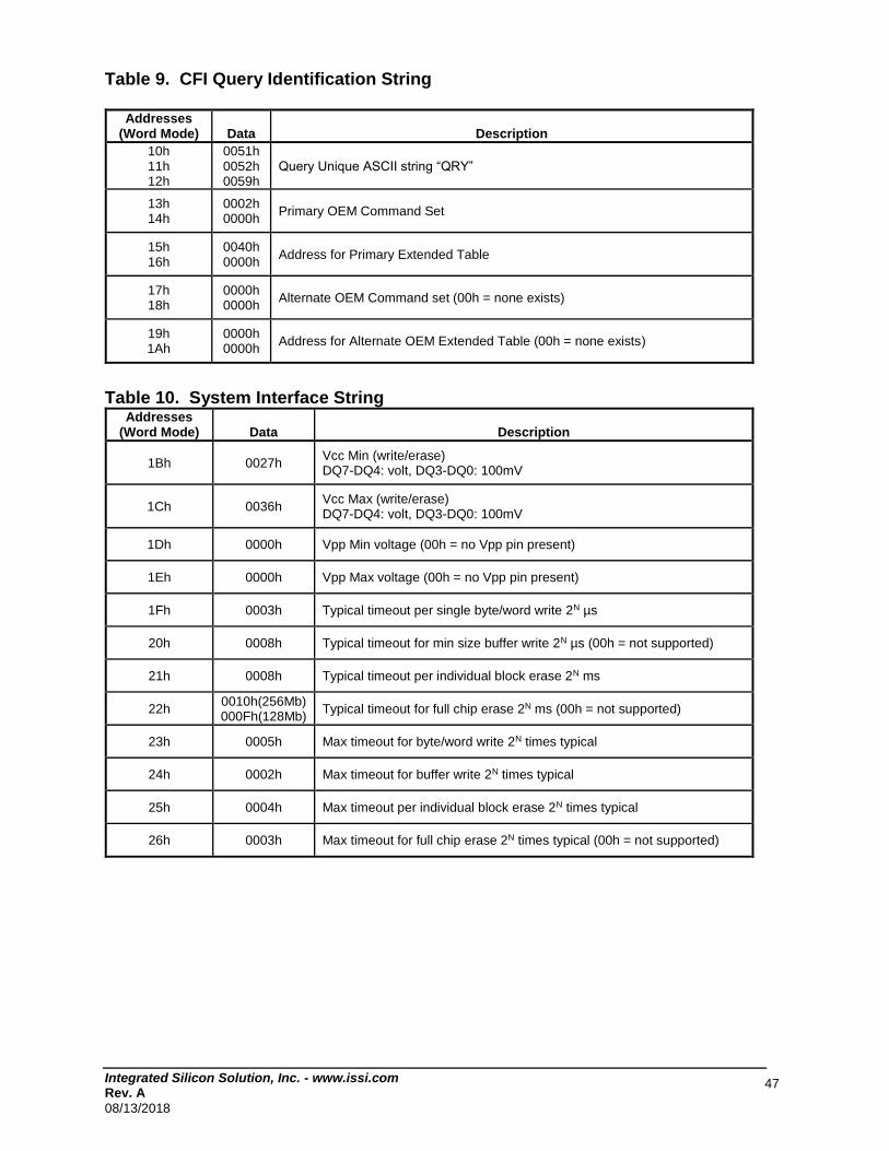
Integrated Silicon Solution, Inc. - www.issi.com Rev. A
08/13/2018
47
Table 9. CFI Query Identification String
Addresses (Word Mode) Data Description
10h 11h 12h
0051h 0052h 0059h
Query Unique ASCII string “QRY”
13h 14h
0002h 0000h
Primary OEM Command Set
15h 16h
0040h 0000h
Address for Primary Extended Table
17h 18h
0000h 0000h
Alternate OEM Command set (00h = none exists)
19h 1Ah
0000h 0000h
Address for Alternate OEM Extended Table (00h = none exists)
Table 10. System Interface String
Addresses (Word Mode) Data Description
1Bh 0027h Vcc Min (write/erase) DQ7-DQ4: volt, DQ3-DQ0: 100mV
1Ch 0036h Vcc Max (write/erase) DQ7-DQ4: volt, DQ3-DQ0: 100mV
1Dh 0000h Vpp Min voltage (00h = no Vpp pin present)
1Eh 0000h Vpp Max voltage (00h = no Vpp pin present)
1Fh 0003h Typical timeout per single byte/word write 2N µs
20h 0008h Typical timeout for min size buffer write 2N µs (00h = not supported)
21h 0008h Typical timeout per individual block erase 2N ms
22h 0010h(256Mb) 000Fh(128Mb)
Typical timeout for full chip erase 2N ms (00h = not supported)
23h 0005h Max timeout for byte/word write 2N times typical
24h 0002h Max timeout for buffer write 2N times typical
25h 0004h Max timeout per individual block erase 2N times typical
26h 0003h Max timeout for full chip erase 2N times typical (00h = not supported)
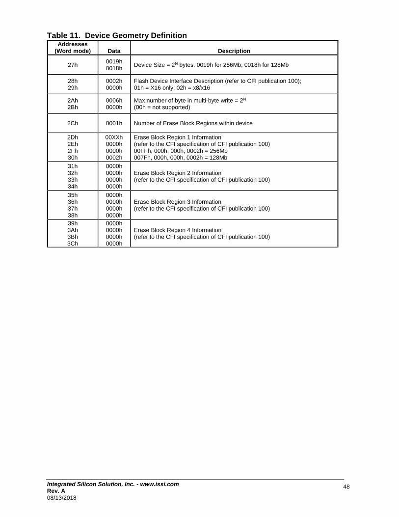
Integrated Silicon Solution, Inc. - www.issi.com Rev. A
08/13/2018
48
Table 11. Device Geometry Definition Addresses
(Word mode) Data Description
27h 0019h 0018h
Device Size = 2N bytes. 0019h for 256Mb, 0018h for 128Mb
28h 29h
0002h 0000h
Flash Device Interface Description (refer to CFI publication 100); 01h = X16 only; 02h = x8/x16
2Ah 2Bh
0006h 0000h
Max number of byte in multi-byte write = 2N (00h = not supported)
2Ch 0001h Number of Erase Block Regions within device
2Dh 2Eh 2Fh 30h
00XXh 0000h 0000h 0002h
Erase Block Region 1 Information (refer to the CFI specification of CFI publication 100) 00FFh, 000h, 000h, 0002h = 256Mb 007Fh, 000h, 000h, 0002h = 128Mb
31h 32h 33h 34h
0000h 0000h 0000h 0000h
Erase Block Region 2 Information (refer to the CFI specification of CFI publication 100)
35h 36h 37h 38h
0000h 0000h 0000h 0000h
Erase Block Region 3 Information (refer to the CFI specification of CFI publication 100)
39h 3Ah 3Bh 3Ch
0000h 0000h 0000h 0000h
Erase Block Region 4 Information (refer to the CFI specification of CFI publication 100)
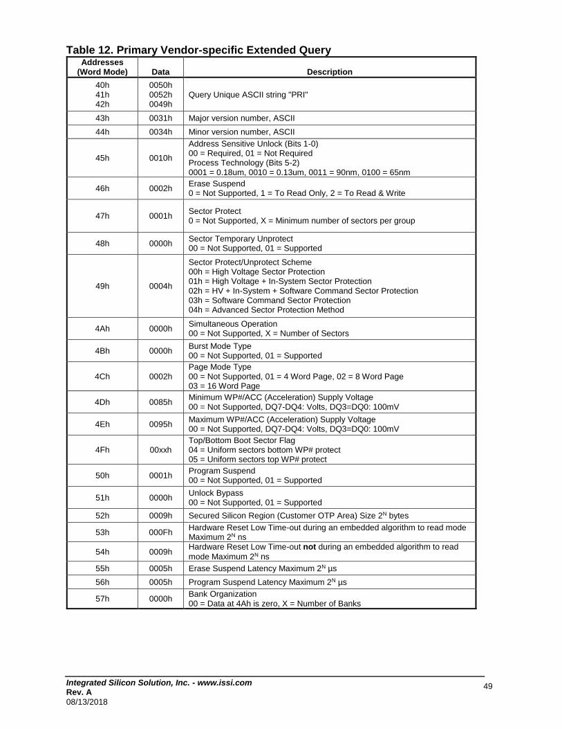
Integrated Silicon Solution, Inc. - www.issi.com Rev. A
08/13/2018
49
Table 12. Primary Vendor-specific Extended Query Addresses
(Word Mode) Data Description
40h 41h 42h
0050h 0052h 0049h
Query Unique ASCII string "PRI"
43h 0031h Major version number, ASCII
44h 0034h Minor version number, ASCII
45h 0010h
Address Sensitive Unlock (Bits 1-0) 00 = Required, 01 = Not Required Process Technology (Bits 5-2) 0001 = 0.18um, 0010 = 0.13um, 0011 = 90nm, 0100 = 65nm
46h 0002h Erase Suspend 0 = Not Supported, 1 = To Read Only, 2 = To Read & Write
47h 0001h Sector Protect 0 = Not Supported, X = Minimum number of sectors per group
48h 0000h Sector Temporary Unprotect 00 = Not Supported, 01 = Supported
49h 0004h
Sector Protect/Unprotect Scheme 00h = High Voltage Sector Protection 01h = High Voltage + In-System Sector Protection 02h = HV + In-System + Software Command Sector Protection 03h = Software Command Sector Protection 04h = Advanced Sector Protection Method
4Ah 0000h Simultaneous Operation 00 = Not Supported, X = Number of Sectors
4Bh 0000h Burst Mode Type 00 = Not Supported, 01 = Supported
4Ch 0002h Page Mode Type 00 = Not Supported, 01 = 4 Word Page, 02 = 8 Word Page 03 = 16 Word Page
4Dh 0085h Minimum WP#/ACC (Acceleration) Supply Voltage 00 = Not Supported, DQ7-DQ4: Volts, DQ3=DQ0: 100mV
4Eh 0095h Maximum WP#/ACC (Acceleration) Supply Voltage 00 = Not Supported, DQ7-DQ4: Volts, DQ3=DQ0: 100mV
4Fh 00xxh Top/Bottom Boot Sector Flag 04 = Uniform sectors bottom WP# protect 05 = Uniform sectors top WP# protect
50h 0001h Program Suspend 00 = Not Supported, 01 = Supported
51h 0000h Unlock Bypass 00 = Not Supported, 01 = Supported
52h 0009h Secured Silicon Region (Customer OTP Area) Size 2N bytes
53h 000Fh Hardware Reset Low Time-out during an embedded algorithm to read mode Maximum 2N ns
54h 0009h Hardware Reset Low Time-out not during an embedded algorithm to read
mode Maximum 2N ns
55h 0005h Erase Suspend Latency Maximum 2N µs
56h 0005h Program Suspend Latency Maximum 2N µs
57h 0000h Bank Organization 00 = Data at 4Ah is zero, X = Number of Banks
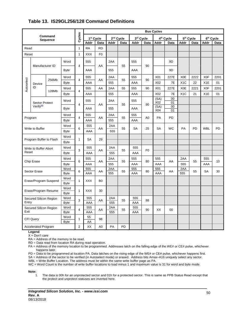
Integrated Silicon Solution, Inc. - www.issi.com Rev. A
08/13/2018
50
Table 13. IS29GL256/128 Command Definitions
Command Sequence
Cycle
s Bus Cycles
1st Cycle 2nd Cycle 3rd Cycle 4th Cycle 5th Cycle 6th Cycle
Addr Data Addr Data Addr Data Addr Data Addr Data Addr Data
Read 1 RA RD
Reset 1 XXX F0
Auto
sele
ct
Manufacturer ID
Word
4
555
AA
2AA
55
555
90
9D
Byte AAA 555 AAA 9D
Device ID
256Mb Word
4 555
AA 2AA
55 555
90 X01 227E X0E 2222 X0F 2201
Byte AAA 555 AAA X02 7E X1C 22 X1E 01
128Mb Word
4 555 AA 2AA 55 555 90 X01 227E X0E 2221 X0F 2201
Byte AAA 555 AAA X02 7E X1C 21 X1E 01
Sector Protect Verify(1)
Word
4
555
AA
2AA
55
555
90
(SA) X02
00
01
Byte AAA 555 AAA (SA) X04
00
01
Program Word
4 555
AA 2AA
55 555
A0 PA PD Byte AAA 555 AAA
Write to Buffer Word
6 555
AA 2AA
55 SA 25 SA WC PA PD WBL PD Byte AAA 555
Program Buffer to Flash Word
1 SA 29
Byte
Write to Buffer Abort Reset
Word 3
555 AA
2AA 55
555 F0
Byte AAA 555 AAA
Chip Erase Word
6 555
AA 2AA
55 555
80 555
AA 2AA
55 555
10 Byte AAA 555 AAA AAA 555 AAA
Sector Erase Word
6 555
AA 2AA
55 555
80 555
AA 2AA
55 SA 30 Byte AAA 555 AAA AAA 555
Erase/Program Suspend Word
1 XXX B0 Byte
Erase/Program Resume Word
1 XXX 30 Byte
Secured Silicon Region Entry
Word 3
555 AA
2AA 55
555 88
Byte AAA 555 AAA
Secured Silicon Region Exit
Word 4
555 AA
2AA 55
555 90 XX 00
Byte AAA 555 AAA
CFI Query Word
1 55
98 Byte AA
Accelerated Program 2 XX A0 PA PD
Legend X = Don’t care RA = Address of the memory to be read. RD = Data read from location RA during read operation. PA = Address of the memory location to be programmed. Addresses latch on the falling edge of the WE# or CE# pulse, whichever
happens later. PD = Data to be programmed at location PA. Data latches on the rising edge of the WE# or CE# pulse, whichever happens first. SA = Address of the sector to be verified (in Autoselect mode) or erased. Address bits Amax–A16 uniquely select any sector. WBL = Write Buffer Location. The address must be within the same write buffer page as PA. WC = Word Count is the number of write buffer locations to load minus 1 and maximum value is 31 for word and byte mode. Note:
1. The data is 00h for an unprotected sector and 01h for a protected sector. This is same as PPB Status Read except that the protect and unprotect statuses are inverted here.
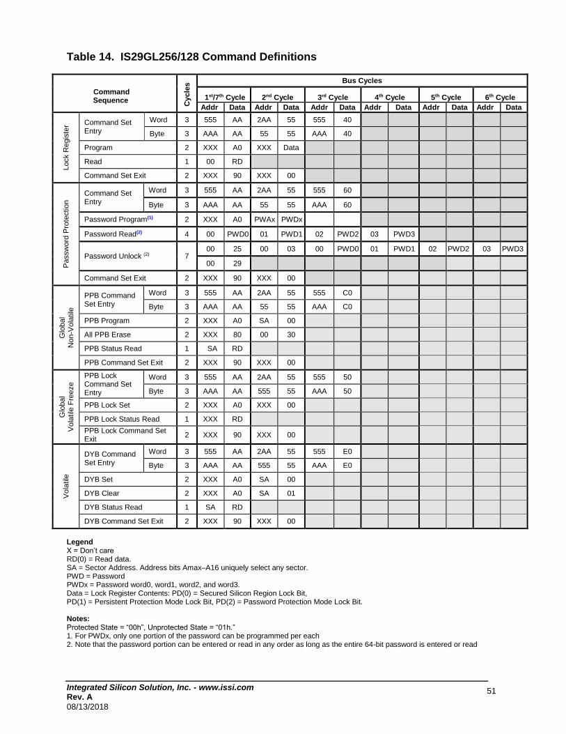
Integrated Silicon Solution, Inc. - www.issi.com Rev. A
08/13/2018
51
Table 14. IS29GL256/128 Command Definitions
Command Sequence
Cycle
s Bus Cycles
1st/7th Cycle 2nd Cycle 3rd Cycle 4th Cycle 5th Cycle 6th Cycle
Addr Data Addr Data Addr Data Addr Data Addr Data Addr Data
Lock R
egis
ter Command Set
Entry
Word 3 555 AA 2AA 55 555 40
Byte 3 AAA AA 55 55 AAA 40
Program 2 XXX A0 XXX Data
Read 1 00 RD
Command Set Exit 2 XXX 90 XXX 00
Passw
ord
Pro
tectio
n
Command Set Entry
Word 3 555 AA 2AA 55 555 60
Byte 3 AAA AA 55 55 AAA 60
Password Program(1) 2 XXX A0 PWAx PWDx
Password Read(2) 4 00 PWD0 01 PWD1 02 PWD2 03 PWD3
Password Unlock (2) 7 00 25 00 03 00 PWD0 01 PWD1 02 PWD2 03 PWD3
00 29
Command Set Exit 2 XXX 90 XXX 00
Glo
bal
Non-V
ola
tile
PPB Command Set Entry
Word 3 555 AA 2AA 55 555 C0
Byte 3 AAA AA 55 55 AAA C0
PPB Program 2 XXX A0 SA 00
All PPB Erase 2 XXX 80 00 30
PPB Status Read 1 SA RD
PPB Command Set Exit 2 XXX 90 XXX 00
Glo
bal
Vola
tile
Fre
eze
PPB Lock Command Set Entry
Word 3 555 AA 2AA 55 555 50
Byte 3 AAA AA 555 55 AAA 50
PPB Lock Set 2 XXX A0 XXX 00
PPB Lock Status Read 1 XXX RD
PPB Lock Command Set Exit
2 XXX 90 XXX 00
Vola
tile
DYB Command Set Entry
Word 3 555 AA 2AA 55 555 E0
Byte 3 AAA AA 555 55 AAA E0
DYB Set 2 XXX A0 SA 00
DYB Clear 2 XXX A0 SA 01
DYB Status Read 1 SA RD
DYB Command Set Exit 2 XXX 90 XXX 00
Legend X = Don’t care RD(0) = Read data. SA = Sector Address. Address bits Amax–A16 uniquely select any sector. PWD = Password PWDx = Password word0, word1, word2, and word3. Data = Lock Register Contents: PD(0) = Secured Silicon Region Lock Bit, PD(1) = Persistent Protection Mode Lock Bit, PD(2) = Password Protection Mode Lock Bit. Notes: Protected State = “00h”, Unprotected State = “01h.” 1. For PWDx, only one portion of the password can be programmed per each 2. Note that the password portion can be entered or read in any order as long as the entire 64-bit password is entered or read
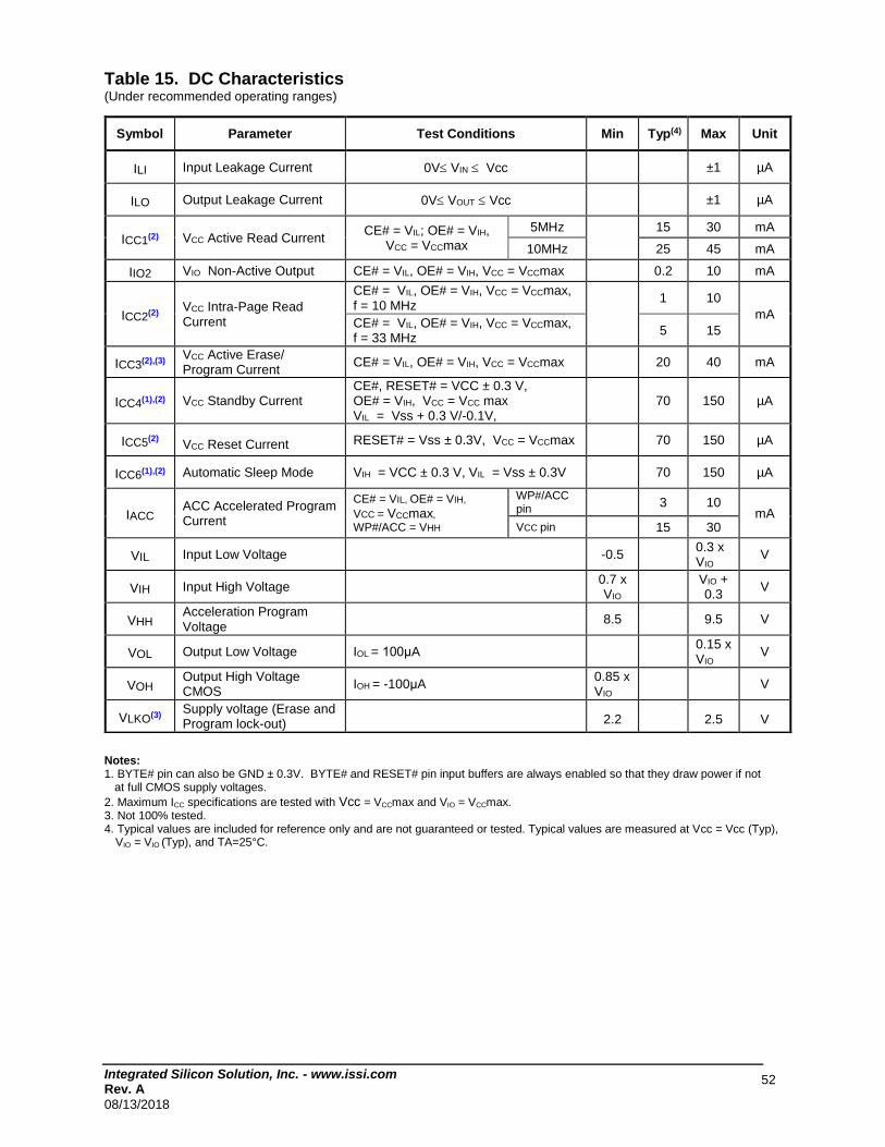
Integrated Silicon Solution, Inc. - www.issi.com Rev. A
08/13/2018
52
Table 15. DC Characteristics (Under recommended operating ranges)
Notes: 1. BYTE# pin can also be GND ± 0.3V. BYTE# and RESET# pin input buffers are always enabled so that they draw power if not
at full CMOS supply voltages.
2. Maximum ICC specifications are tested with Vcc = VCCmax and VIO = VCCmax. 3. Not 100% tested. 4. Typical values are included for reference only and are not guaranteed or tested. Typical values are measured at Vcc = Vcc (Typ),
VIO = VIO (Typ), and TA=25°C.
Symbol Parameter Test Conditions Min Typ(4) Max Unit
ILI Input Leakage Current 0V VIN Vcc ±1 µA
ILO Output Leakage Current 0V VOUT Vcc ±1 µA
ICC1(2) VCC Active Read Current CE# = VIL; OE# = VIH,
VCC = VCCmax
5MHz
15 30 mA
10MHz 25 45 mA
IIO2 VIO Non-Active Output CE# = VIL, OE# = VIH, VCC = VCCmax 0.2 10 mA
ICC2(2)
VCC Intra-Page Read Current
CE# = VIL, OE# = VIH, VCC = VCCmax, f = 10 MHz
1 10
mA CE# = VIL, OE# = VIH, VCC = VCCmax, f = 33 MHz
5 15
ICC3(2),(3) VCC Active Erase/ Program Current
CE# = VIL, OE# = VIH, VCC = VCCmax 20 40 mA
ICC4(1),(2)
VCC Standby Current CE#, RESET# = VCC ± 0.3 V, OE# = VIH, VCC = VCC max VIL = Vss + 0.3 V/-0.1V,
70 150 µA
ICC5(2) VCC Reset Current RESET# = Vss ± 0.3V, VCC = VCCmax 70 150 µA
ICC6(1),(2)
Automatic Sleep Mode VIH = VCC ± 0.3 V, VIL = Vss ± 0.3V 70 150 µA
IACC ACC Accelerated Program Current
CE# = VIL, OE# = VIH,
VCC = VCCmax,
WP#/ACC = VHH
WP#/ACC pin 3 10
mA VCC pin 15 30
VIL Input Low Voltage -0.5
0.3 x VIO
V
VIH Input High Voltage
0.7 x VIO
VIO + 0.3
V
VHH
Acceleration Program Voltage
8.5 9.5 V
VOL Output Low Voltage IOL = 100μA
0.15 x VIO
V
VOH
Output High Voltage CMOS
IOH = -100μA 0.85 x VIO
V
VLKO(3)
Supply voltage (Erase and Program lock-out)
2.2 2.5 V
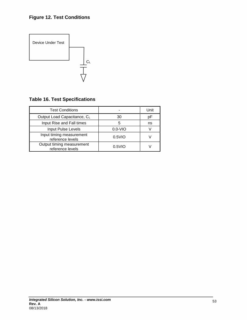
Integrated Silicon Solution, Inc. - www.issi.com Rev. A
08/13/2018
53
Figure 12. Test Conditions
Table 16. Test Specifications
Test Conditions - Unit
Output Load Capacitance, C BLB 30 pF
Input Rise and Fall times 5 ns
Input Pulse Levels 0.0-VIO V
Input timing measurement reference levels
0.5VIO V
Output timing measurement reference levels
0.5VIO V
CL
Device Under Test
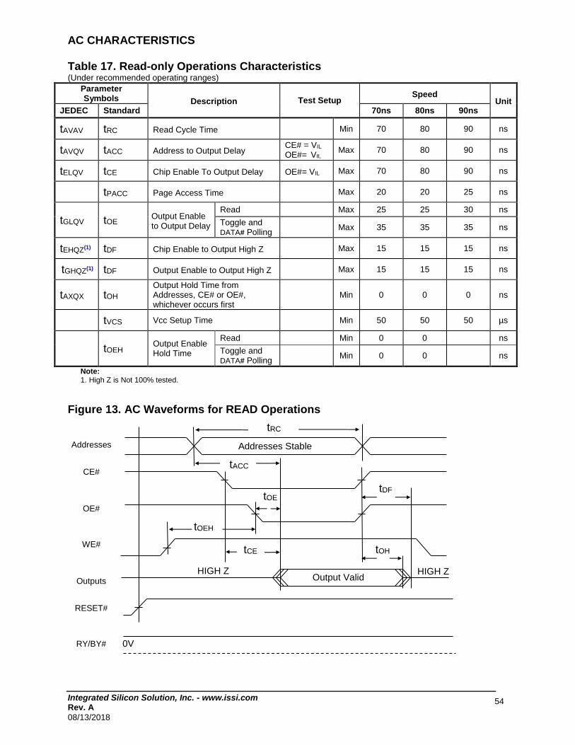
Integrated Silicon Solution, Inc. - www.issi.com Rev. A
08/13/2018
54
AC CHARACTERISTICS Table 17. Read-only Operations Characteristics
(Under recommended operating ranges)
Parameter Symbols Description Test Setup
Speed Unit
JEDEC Standard 70ns 80ns 90ns
tAVAV tRC Read Cycle Time Min 70 80 90 ns
tAVQV tACC Address to Output Delay CE# = VIL
OE#= VIL Max 70 80 90 ns
tELQV tCE Chip Enable To Output Delay OE#= VIL Max 70 80 90 ns
tPACC Page Access Time Max 20 20 25 ns
tGLQV tOE Output Enable to Output Delay
Read Max 25 25 30 ns
Toggle and DATA# Polling
Max 35 35 35 ns
tEHQZ(1) tDF Chip Enable to Output High Z Max 15 15 15 ns
tGHQZ(1) tDF Output Enable to Output High Z Max 15 15 15 ns
tAXQX tOH
Output Hold Time from Addresses, CE# or OE#, whichever occurs first
Min 0 0 0 ns
tVCS Vcc Setup Time Min 50 50 50 µs
tOEH Output Enable Hold Time
Read Min 0 0 ns
Toggle and DATA# Polling
Min 0 0 ns
Note: 1. High Z is Not 100% tested.
Figure 13. AC Waveforms for READ Operations
Addresses
CE#
OE#
WE#
Outputs
RESET#
RY/BY#
t BACC
0V
HIGH Z Output Valid
t BCEB t BOH
t BDF
t BOEHB
HIGH Z
t BOEB
t BRCB
Addresses Stable

Integrated Silicon Solution, Inc. - www.issi.com Rev. A
08/13/2018
55
Figure 14. Page Read Operation Timings
Note: Addresses are A2:A-1 for byte mode.
A23
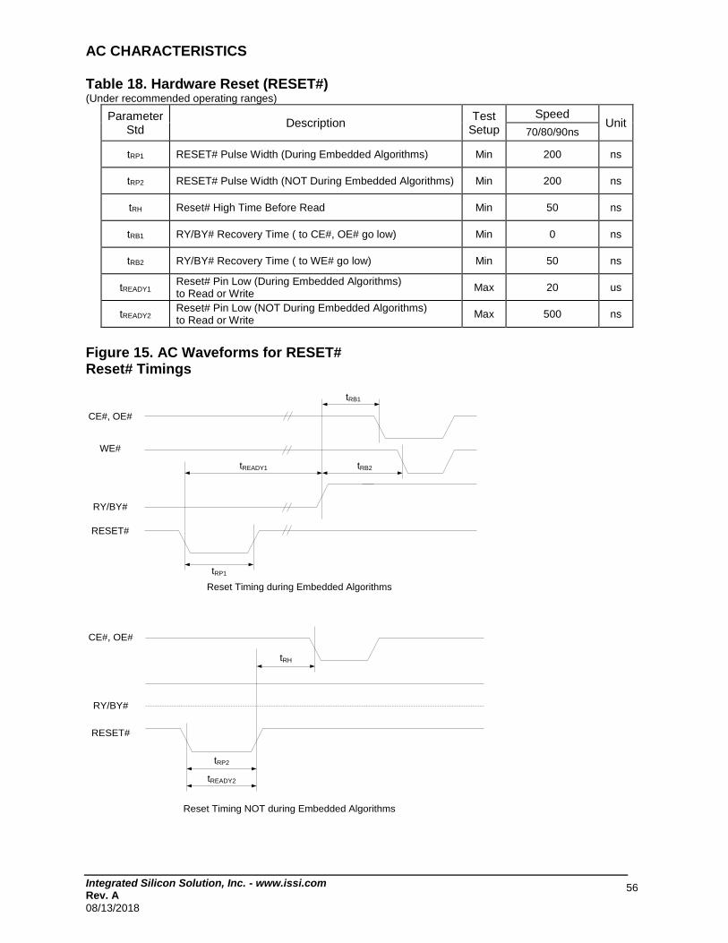
Integrated Silicon Solution, Inc. - www.issi.com Rev. A
08/13/2018
56
AC CHARACTERISTICS Table 18. Hardware Reset (RESET#) (Under recommended operating ranges)
Parameter Std
Description Test
Setup
Speed Unit
70/80/90ns
tRP1 RESET# Pulse Width (During Embedded Algorithms) Min 200 ns
tRP2 RESET# Pulse Width (NOT During Embedded Algorithms) Min 200 ns
tRH Reset# High Time Before Read Min 50 ns
tRB1 RY/BY# Recovery Time ( to CE#, OE# go low) Min 0 ns
tRB2 RY/BY# Recovery Time ( to WE# go low) Min 50 ns
tREADY1 Reset# Pin Low (During Embedded Algorithms) to Read or Write
Max 20 us
tREADY2 Reset# Pin Low (NOT During Embedded Algorithms) to Read or Write
Max 500 ns
Figure 15. AC Waveforms for RESET# Reset# Timings
CE#, OE#
WE#
RY/BY#
RESET#
tRP1
tREADY1 tRB2
tRB1
Reset Timing during Embedded Algorithms
RESET#
RY/BY#
CE#, OE#
tREADY2
tRH
tRP2
Reset Timing NOT during Embedded Algorithms
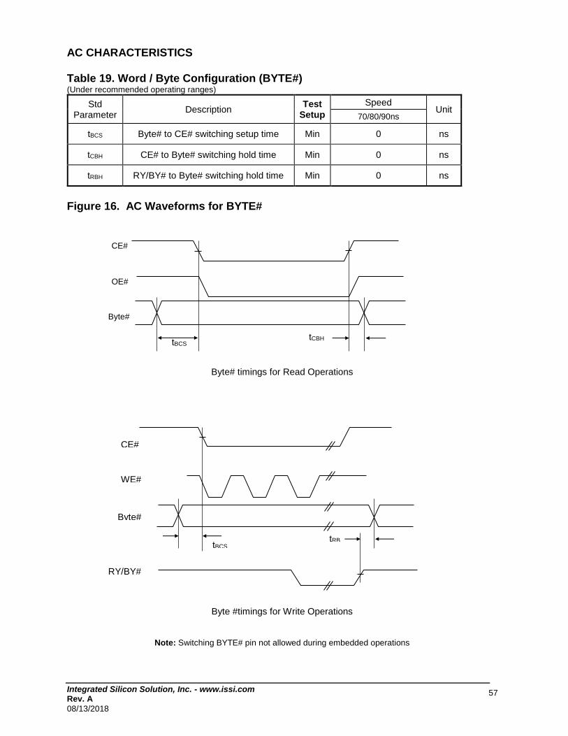
Integrated Silicon Solution, Inc. - www.issi.com Rev. A
08/13/2018
57
AC CHARACTERISTICS Table 19. Word / Byte Configuration (BYTE#) (Under recommended operating ranges)
Std Parameter
Description Test
Setup
Speed Unit
70/80/90ns
tBCS Byte# to CE# switching setup time Min 0 ns
tCBH CE# to Byte# switching hold time Min 0 ns
tRBH RY/BY# to Byte# switching hold time Min 0 ns
Figure 16. AC Waveforms for BYTE#
Byte# timings for Read Operations
Byte #timings for Write Operations
Note: Switching BYTE# pin not allowed during embedded operations
CE#
WE#
tBCS
Byte#
tRB
H
RY/BY#
tCBH tBCS
CE#
OE#
Byte#
Integrated Silicon Solution, Inc. - www.issi.com Rev. A
08/13/2018
58
AC CHARACTERISTICS Table 20. Write (Erase/Program) Operations
(Under recommended operating ranges)
Parameter Symbols
Description Speed(1)
Unit JEDEC
Standard
70ns 80ns 90ns
tAVAV tWC Write Cycle Time Min 70 80 90 ns
tAVWL tAS Address Setup Time Min 0 0 0 ns
tWLAX tAH Address Hold Time Min 45 45 45 ns
tDVWH tDS Data Setup Time Min 30 30 30 ns
tWHDX tDH Data Hold Time Min 0 0 0 ns
tOEH
Output Enable Hold Time
Read MIn 0 0 0 ns
Toggle and DATA# Polling
Min 10 10 10 ns
tGHWL tGHWL
Read Recovery Time before Write (OE# High to WE# Low)
Min 0 0 0 ns
tELWL tCS CE# SetupTime Min 0 0 0 ns
tWHEH tCH CE# Hold Time Min 0 0 0 ns
tWLWH tWP Write Pulse Width Min 25 25 25 ns
tWHDL tWPH Write Pulse Width High Min 20 20 20 ns
tWHWH1 tWHWH1
Write Buffer Program Operation (2, 3)
Typ 160 160 160 µs
Programming Operation (Word and Byte Mode)
Typ(4) 8 8 8 µs
Max 200 200 200 µs
tWHWH2 tWHWH2
Sector Erase Operation
Typ(4) 0.2 0.2 0.2 s
Max 2 2 2 s
Chip Erase Operation
128Mb Typ(4)
30 30 30 s
256Mb 60 60 60
tVHH VHH Rise and Fall Time Min 250 250 250 ns
tVCS Vcc Setup Time Min 50 50 50 µs
tBBUSY WE# High to RY/BY# Low Max 70 70 70 ns
tRB Recovery Time from RY/BY#
Min 0 0 0 ns
Notes: 1. Not 100% tested. 2. See table.22 Erase and Programming Performance for more information. 3. For 1~32 words program. 4. Typical values are included for reference only and are not guaranteed or tested. Typical values
are measured at Vcc = Vcc (Typ), VIO = VIO (Typ), and TA=25°C.
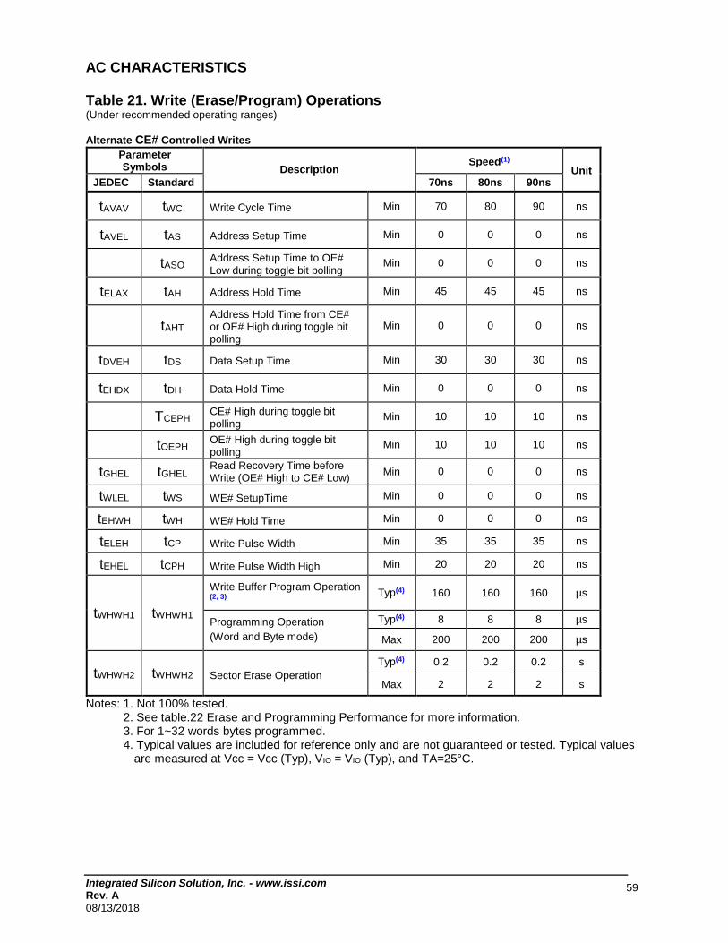
Integrated Silicon Solution, Inc. - www.issi.com Rev. A
08/13/2018
59
AC CHARACTERISTICS Table 21. Write (Erase/Program) Operations (Under recommended operating ranges)
Alternate CE# Controlled Writes Parameter Symbols Description
Speed(1) Unit
JEDEC Standard 70ns 80ns 90ns
tAVAV tWC Write Cycle Time Min 70 80 90 ns
tAVEL tAS Address Setup Time Min 0 0 0 ns
tASO Address Setup Time to OE# Low during toggle bit polling
Min 0 0 0 ns
tELAX tAH Address Hold Time Min 45 45 45 ns
tAHT Address Hold Time from CE# or OE# High during toggle bit polling
Min 0 0 0 ns
tDVEH tDS Data Setup Time Min 30 30 30 ns
tEHDX tDH Data Hold Time Min 0 0 0 ns
TCEPH CE# High during toggle bit polling
Min 10 10 10 ns
tOEPH OE# High during toggle bit polling
Min 10 10 10 ns
tGHEL tGHEL Read Recovery Time before Write (OE# High to CE# Low)
Min 0 0 0 ns
tWLEL tWS WE# SetupTime Min 0 0 0 ns
tEHWH tWH WE# Hold Time Min 0 0 0 ns
tELEH tCP Write Pulse Width Min 35 35 35 ns
tEHEL tCPH Write Pulse Width High Min 20 20 20 ns
tWHWH1 tWHWH1
Write Buffer Program Operation (2, 3)
Typ(4) 160 160 160 µs
Programming Operation
(Word and Byte mode)
Typ(4) 8 8 8 µs
Max 200 200 200 µs
tWHWH2 tWHWH2 Sector Erase Operation
Typ(4) 0.2 0.2 0.2 s
Max 2 2 2 s
Notes: 1. Not 100% tested. 2. See table.22 Erase and Programming Performance for more information. 3. For 1~32 words bytes programmed. 4. Typical values are included for reference only and are not guaranteed or tested. Typical values
are measured at Vcc = Vcc (Typ), VIO = VIO (Typ), and TA=25°C.
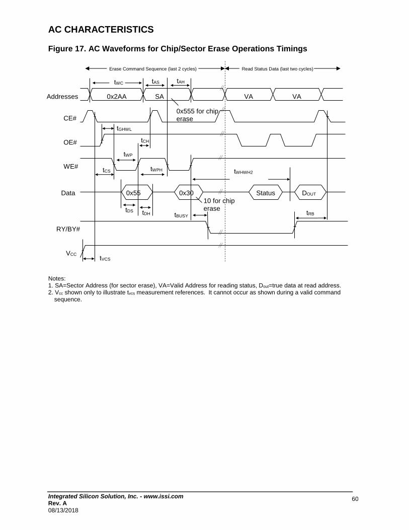
Integrated Silicon Solution, Inc. - www.issi.com Rev. A
08/13/2018
60
AC CHARACTERISTICS Figure 17. AC Waveforms for Chip/Sector Erase Operations Timings Notes: 1. SA=Sector Address (for sector erase), VA=Valid Address for reading status, Dout=true data at read address. 2. Vcc shown only to illustrate tvcs measurement references. It cannot occur as shown during a valid command
sequence.
10 for chip erase
tDH tDS
0x55 0x30 Status DOUT
tWHWH2
VCC
Addresseses
CE#
OE#
WE#
Data
RY/BY#
tCH
tGHWL
tCS
tWPH
tWP
tBUSY tRB
tVCS
Erase Command Sequence (last 2 cycles) Read Status Data (last two cycles)
tAH tWC
0x2AA SA VA VA
tAS
0x555 for chip erase
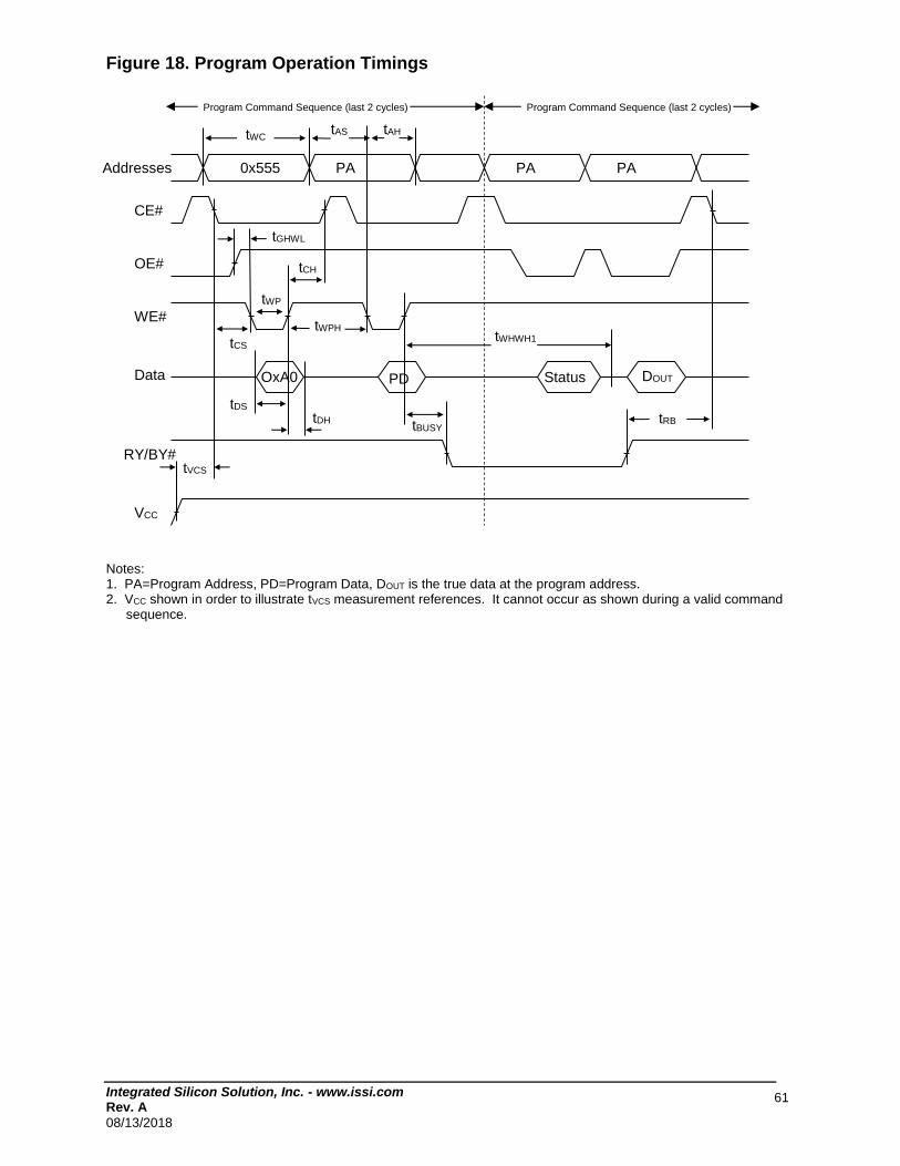
Integrated Silicon Solution, Inc. - www.issi.com Rev. A
08/13/2018
61
Figure 18. Program Operation Timings Notes: 1. PA=Program Address, PD=Program Data, DOUT is the true data at the program address. 2. VCC shown in order to illustrate tVCS measurement references. It cannot occur as shown during a valid command
sequence.
tVCS
tWHWH1
tBUSY
tDS tDH
DOUT Status PD OxA0
tRB
tAH tAS tWC
0x555 PA PA PA
Program Command Sequence (last 2 cycles) Program Command Sequence (last 2 cycles)
tGHWL
Data
RY/BY#
VCC
WE#
Addresses
CE#
OE# tCH
tWPH
tCS
tWP
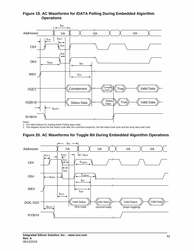
Integrated Silicon Solution, Inc. - www.issi.com Rev. A
08/13/2018
62
Figure 19. AC Waveforms for /DATA Polling During Embedded Algorithm Operations
Notes: 1. VA=Valid Address for reading Data# Polling status data 2. This diagram shows the first status cycle after the command sequence, the last status read cycle and the array data read cycle. Figure 20. AC Waveforms for Toggle Bit During Embedded Algorithm Operations
tBUSY
tOEH tDF
tOE
tCE
tCH tACC
tRC
VA VA VA
tOH
Valid Data True Complement Comple-ment
Status Data Status Data
True Valid Data
CE#
Addresses
OE#
WE#
DQ[7]
DQ[6:0]
RY/BY#
tCE
tOE
tCH
Valid Data Valid Status Valid Status Valid Status
(first read) (second read) (stops toggling)
Addresses
CE#
OE#
WE#
DQ6, DQ2
RY/BY#
tRC
tACC
VA VA VA VA
tOEH tDF
tOH
tBUSY
tAHT tASO
TCEPH
TOEPH
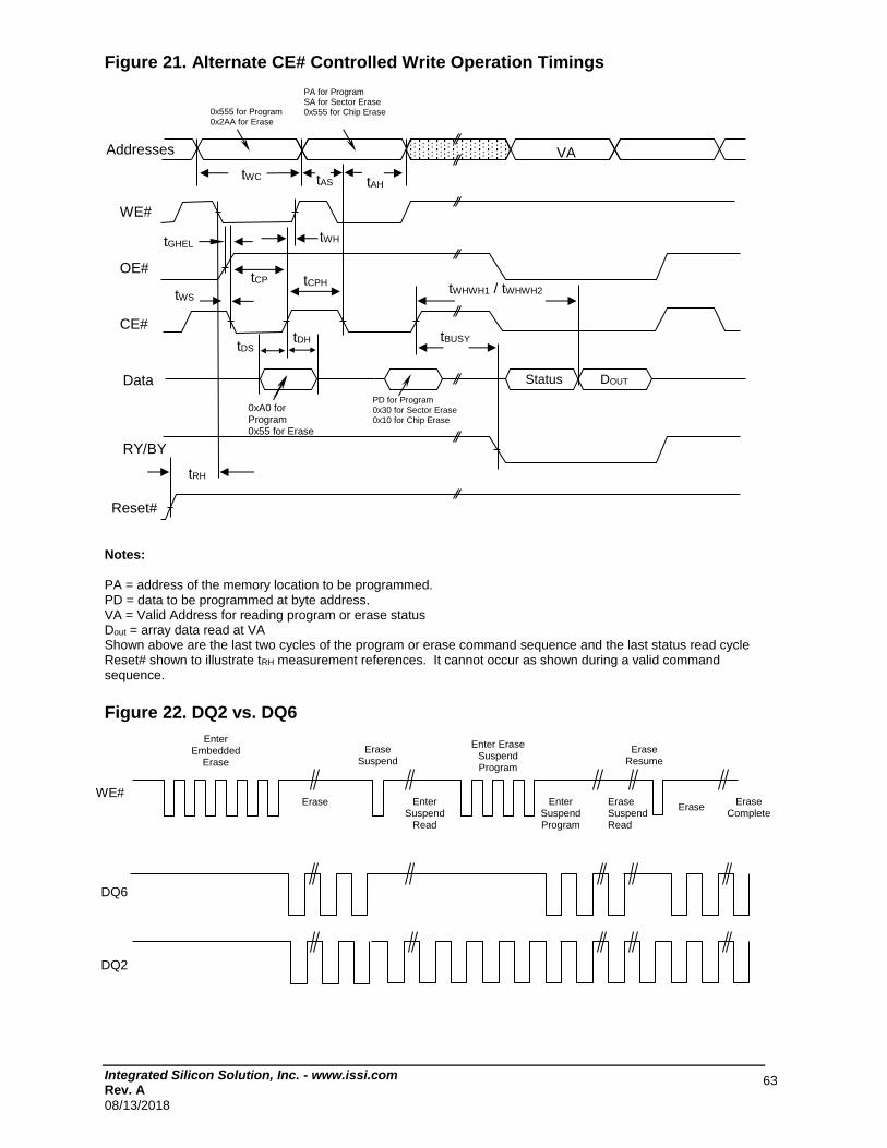
Integrated Silicon Solution, Inc. - www.issi.com Rev. A
08/13/2018
63
Figure 21. Alternate CE# Controlled Write Operation Timings
Notes:
PA = address of the memory location to be programmed. PD = data to be programmed at byte address. VA = Valid Address for reading program or erase status Dout = array data read at VA Shown above are the last two cycles of the program or erase command sequence and the last status read cycle Reset# shown to illustrate tRH measurement references. It cannot occur as shown during a valid command sequence.
Figure 22. DQ2 vs. DQ6
WE#
DQ6
DQ2
Enter Embedded
Erase
Erase Suspend
Enter Erase Suspend Program
Erase Resume
Erase Enter Suspend
Read
Enter Suspend Program
Erase Erase
Complete Erase Suspend Read
tRH
tWH tGHEL
tCP
PD for Program 0x30 for Sector Erase 0x10 for Chip Erase
0xA0 for Program 0x55 for Erase
DOUT Status
tBUSY tDS
tDH
tCPH tWS tWHWH1 / tWHWH2
Addresses
WE#
OE#
CE#
Data
RY/BY#
Reset#
tAH tAS tWC
VA
PA for Program SA for Sector Erase 0x555 for Chip Erase 0x555 for Program
0x2AA for Erase
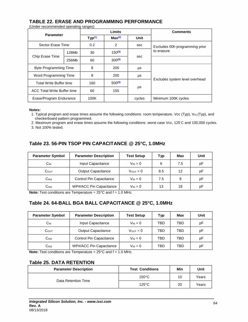
Integrated Silicon Solution, Inc. - www.issi.com Rev. A
08/13/2018
64
TABLE 22. ERASE AND PROGRAMMING PERFORMANCE (Under recommended operating ranges)
Parameter Limits Comments
Typ(1) Max(2) Unit
Sector Erase Time 0.2 2 sec Excludes 00h programming prior to erasure
Chip Erase Time 128Mb 30 150(3)
sec 256Mb 60 300(3)
Byte Programming Time 8 200 µs
Excludes system level overhead Word Programming Time 8 200 µs
Total Write Buffer time 160 500(3) µs
ACC Total Write Buffer time 60 150
Erase/Program Endurance 100K cycles Minimum 100K cycles
Notes:
1. Typical program and erase times assume the following conditions: room temperature, Vcc (Typ), VIO (Typ), and checkerboard pattern programmed.
2. Maximum program and erase times assume the following conditions: worst case Vcc, 125°C and 100,000 cycles.
3. Not 100% tested.
Table 23. 56-PIN TSOP PIN CAPACITANCE @ 25°C, 1.0MHz
Parameter Symbol Parameter Description Test Setup Typ Max Unit
CIN Input Capacitance VIN = 0 6 7.5 pF
COUT Output Capacitance VOUT = 0 8.5 12 pF
CIN2 Control Pin Capacitance VIN = 0 7.5 9 pF
CIN3 WP#/ACC Pin Capacitance VIN = 0 13 18 pF
Note: Test conditions are Temperature = 25°C and f = 1.0 MHz. Table 24. 64-BALL BGA BALL CAPACITANCE @ 25°C, 1.0MHz
Parameter Symbol Parameter Description Test Setup Typ Max Unit
CIN Input Capacitance VIN = 0 TBD TBD pF
COUT Output Capacitance VOUT = 0 TBD TBD pF
CIN2 Control Pin Capacitance VIN = 0 TBD TBD pF
CIN3 WP#/ACC Pin Capacitance VIN = 0 TBD TBD pF
Note: Test conditions are Temperature = 25°C and f = 1.0 MHz. Table 25. DATA RETENTION
Parameter Description Test Conditions Min Unit
Data Retention Time 150°C 10 Years
125°C 20 Years
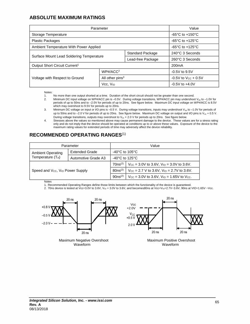
Integrated Silicon Solution, Inc. - www.issi.com Rev. A
08/13/2018
65
ABSOLUTE MAXIMUM RATINGS
Parameter Value
Storage Temperature -65°C to +150°C
Plastic Packages -65°C to +125°C
Ambient Temperature With Power Applied -65°C to +125°C
Surface Mount Lead Soldering Temperature Standard Package 240°C 3 Seconds
Lead-free Package 260°C 3 Seconds
Output Short Circuit Current1 200mA
Voltage with Respect to Ground
WP#/ACC2 -0.5V to 9.5V
All other pins3 -0.5V to VCC + 0.5V
Vcc, VIO -0.5V to +4.0V
Notes: 1. No more than one output shorted at a time. Duration of the short circuit should not be greater than one second.
2. Minimum DC input voltage on WP#/ACC pin is –0.5V. During voltage transitions, WP#/ACC pin may undershoot Vss to –1.0V for
periods of up to 50ns and to –2.0V for periods of up to 20ns. See figure below. Maximum DC input voltage on WP#/ACC is 8.5V
which may overshoot to 9.5V for periods up to 20ns.
3. Minimum DC voltage on input or I/O pins is –0.5 V. During voltage transitions, inputs may undershoot Vss to –1.0V for periods of
up to 50ns and to –2.0 V for periods of up to 20ns. See figure below. Maximum DC voltage on output and I/O pins is Vcc + 0.5 V.
During voltage transitions, outputs may overshoot to Vcc + 2.0 V for periods up to 20ns. See figure below.
4. Stresses above the values so mentioned above may cause permanent damage to the device. These values are for a stress rating only and do not imply that the device should be operated at conditions up to or above these values. Exposure of the device to the maximum rating values for extended periods of time may adversely affect the device reliability.
RECOMMENDED OPERATING RANGES(1)
Parameter Value
Ambient Operating Temperature (TA)
Extended Grade -40°C to 105°C
Automotive Grade A3 -40°C to 125°C
Speed and VCC, VIO Power Supply
70ns(2) VCC = 3.0V to 3.6V, VIO = 3.0V to 3.6V.
80ns(2) VCC = 2.7 V to 3.6V, VIO = 2.7V to 3.6V.
90ns(2) VCC = 3.0V to 3.6V, VIO = 1.65V to VCC.
Notes 1. Recommended Operating Ranges define those limits between which the functionality of the device is guaranteed. 2. 70ns device is tested at Vcc=3.0V to 3.6V, VIO = 3.0V to 3.6V, and becomes80ns at Vcc=VIO=2.7V~3.6V, 90ns at VIO=1.65V ~Vcc.
Vcc
+2.0V
Maximum Negative Overshoot Maximum Positive Overshoot Waveform Waveform
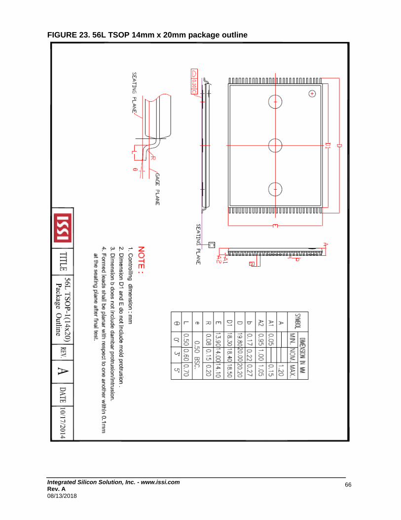
Integrated Silicon Solution, Inc. - www.issi.com Rev. A
08/13/2018
66
FIGURE 23. 56L TSOP 14mm x 20mm package outline
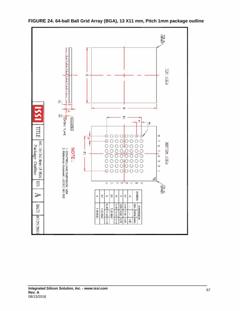
Integrated Silicon Solution, Inc. - www.issi.com Rev. A
08/13/2018
67
FIGURE 24. 64-ball Ball Grid Array (BGA), 13 X11 mm, Pitch 1mm package outline
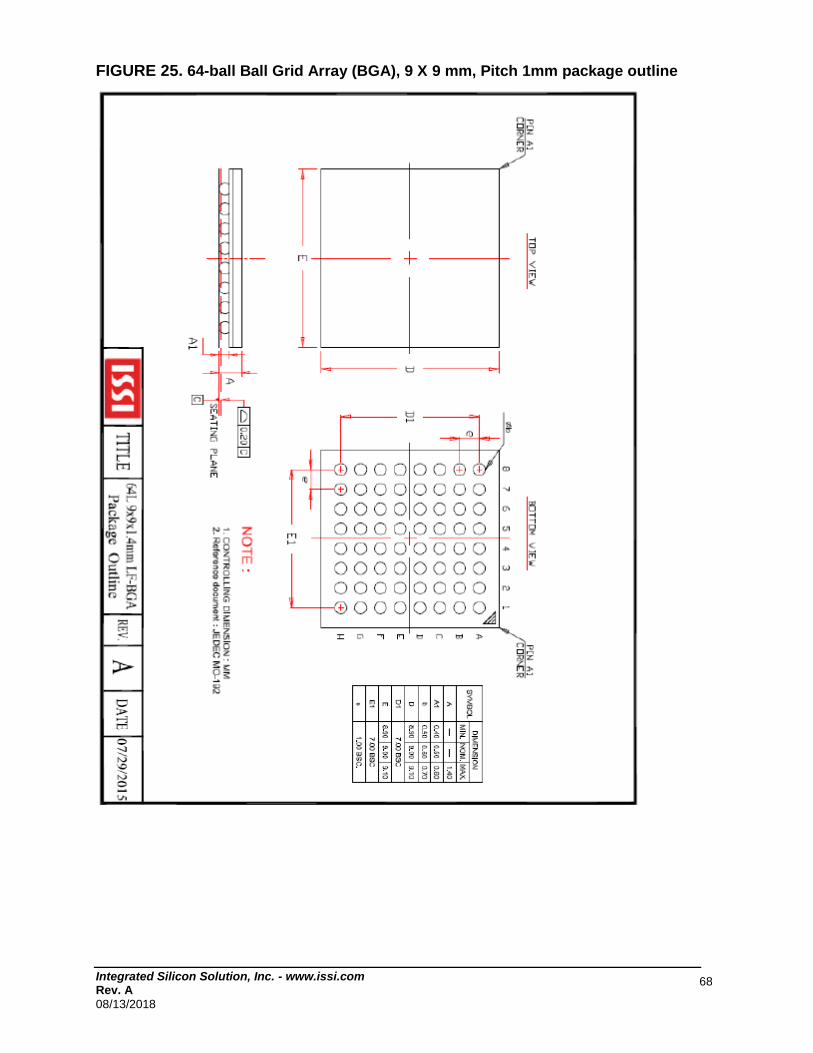
Integrated Silicon Solution, Inc. - www.issi.com Rev. A
08/13/2018
68
FIGURE 25. 64-ball Ball Grid Array (BGA), 9 X 9 mm, Pitch 1mm package outline
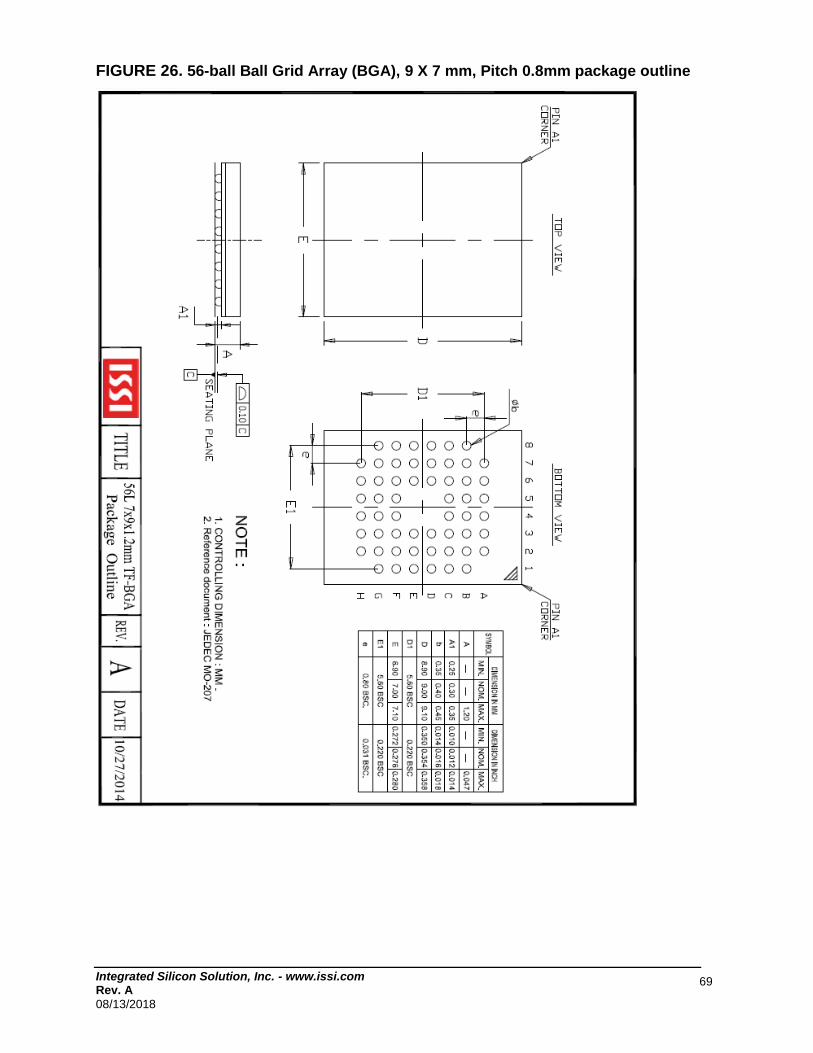
Integrated Silicon Solution, Inc. - www.issi.com Rev. A
08/13/2018
69
FIGURE 26. 56-ball Ball Grid Array (BGA), 9 X 7 mm, Pitch 0.8mm package outline

Integrated Silicon Solution, Inc. - www.issi.com Rev. A
08/13/2018
70
ORDERING INFORMATION IS29GL 256 - 70 D L E T
SECTOR for WRITE PROTECT (WP#/ACC=L)
T = highest address sector protected
B = lowest address sector protected H = highest address sector protected, No BYTE# (1)
L = lowest address sector protected, No BYTE# (1)
TEMPERATURE RANGE
E = Extended (-40°C to +105°C)
A3 = Automotive Grade (-40°C to +125°C)
PACKAGING CONTENT
L = RoHS compliant PACKAGE
S = 56-pin TSOP F = 64-ball BGA 1.0mm pitch, 13mm x 11mm D = 64-ball BGA 1.0mm pitch, 9mm x 9mm G = 56-ball BGA 0.8mm pitch, 9mm x 7mm (Call Factory) W = KGD (Call Factory) SPEED
70 = 70ns (2) at Vcc=3.0~3.6V, VI/O=3.0~3.6V Density
128 =128 Mb 256 =256 Mb BASE PART NUMBER IS = Integrated Silicon Solution Inc.
29GL = FLASH, 3V Page Mode Flash Memory
Notes: 1. No BYTE# device supports x16 org. only.
2. Maximum speed becomes 80ns when Vcc = 2.7V ~ 3.6V, VIO = 2.7V ~ 3.6V, and 90ns when Vcc = 2.7V ~ 3.6V, VIO = 1.65V~Vcc.
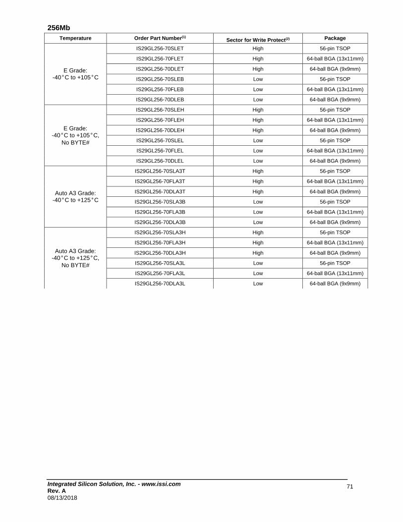
Integrated Silicon Solution, Inc. - www.issi.com Rev. A
08/13/2018
71
256Mb
Temperature Order Part Number(1) Sector for Write Protect(2) Package
E Grade: -40°C to +105°C
IS29GL256-70SLET High 56-pin TSOP
IS29GL256-70FLET High 64-ball BGA (13x11mm)
IS29GL256-70DLET High 64-ball BGA (9x9mm)
IS29GL256-70SLEB Low 56-pin TSOP
IS29GL256-70FLEB Low 64-ball BGA (13x11mm)
IS29GL256-70DLEB Low 64-ball BGA (9x9mm)
E Grade: -40°C to +105°C,
No BYTE#
IS29GL256-70SLEH High 56-pin TSOP
IS29GL256-70FLEH High 64-ball BGA (13x11mm)
IS29GL256-70DLEH High 64-ball BGA (9x9mm)
IS29GL256-70SLEL Low 56-pin TSOP
IS29GL256-70FLEL Low 64-ball BGA (13x11mm)
IS29GL256-70DLEL Low 64-ball BGA (9x9mm)
Auto A3 Grade: -40°C to +125°C
IS29GL256-70SLA3T High 56-pin TSOP
IS29GL256-70FLA3T High 64-ball BGA (13x11mm)
IS29GL256-70DLA3T High 64-ball BGA (9x9mm)
IS29GL256-70SLA3B Low 56-pin TSOP
IS29GL256-70FLA3B Low 64-ball BGA (13x11mm)
IS29GL256-70DLA3B Low 64-ball BGA (9x9mm)
Auto A3 Grade: -40°C to +125°C,
No BYTE#
IS29GL256-70SLA3H High 56-pin TSOP
IS29GL256-70FLA3H High 64-ball BGA (13x11mm)
IS29GL256-70DLA3H High 64-ball BGA (9x9mm)
IS29GL256-70SLA3L Low 56-pin TSOP
IS29GL256-70FLA3L Low 64-ball BGA (13x11mm)
IS29GL256-70DLA3L Low 64-ball BGA (9x9mm)
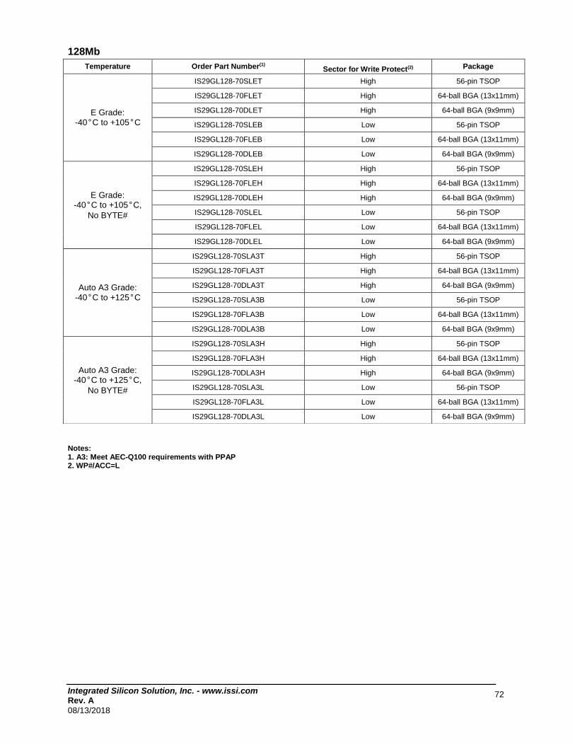
Integrated Silicon Solution, Inc. - www.issi.com Rev. A
08/13/2018
72
128Mb
Notes: 1. A3: Meet AEC-Q100 requirements with PPAP 2. WP#/ACC=L
Temperature Order Part Number(1) Sector for Write Protect(2) Package
E Grade:
-40°C to +105°C
IS29GL128-70SLET High 56-pin TSOP
IS29GL128-70FLET High 64-ball BGA (13x11mm)
IS29GL128-70DLET High 64-ball BGA (9x9mm)
IS29GL128-70SLEB Low 56-pin TSOP
IS29GL128-70FLEB Low 64-ball BGA (13x11mm)
IS29GL128-70DLEB Low 64-ball BGA (9x9mm)
E Grade: -40°C to +105°C,
No BYTE#
IS29GL128-70SLEH High 56-pin TSOP
IS29GL128-70FLEH High 64-ball BGA (13x11mm)
IS29GL128-70DLEH High 64-ball BGA (9x9mm)
IS29GL128-70SLEL Low 56-pin TSOP
IS29GL128-70FLEL Low 64-ball BGA (13x11mm)
IS29GL128-70DLEL Low 64-ball BGA (9x9mm)
Auto A3 Grade:
-40°C to +125°C
IS29GL128-70SLA3T High 56-pin TSOP
IS29GL128-70FLA3T High 64-ball BGA (13x11mm)
IS29GL128-70DLA3T High 64-ball BGA (9x9mm)
IS29GL128-70SLA3B Low 56-pin TSOP
IS29GL128-70FLA3B Low 64-ball BGA (13x11mm)
IS29GL128-70DLA3B Low 64-ball BGA (9x9mm)
Auto A3 Grade: -40°C to +125°C,
No BYTE#
IS29GL128-70SLA3H High 56-pin TSOP
IS29GL128-70FLA3H High 64-ball BGA (13x11mm)
IS29GL128-70DLA3H High 64-ball BGA (9x9mm)
IS29GL128-70SLA3L Low 56-pin TSOP
IS29GL128-70FLA3L Low 64-ball BGA (13x11mm)
IS29GL128-70DLA3L Low 64-ball BGA (9x9mm)