iraudps3-30v +/-30v power supply for class-d audio amplifier
TRANSCRIPT
Rev. 1.2 6/23/2015 International Rectifier Page 1 of 20
PROPRIETARY INFORMATION - This document and the information contained therein are proprietary and are not to be reproduced, used or disclosed to others for manufacture or any other purpose except as specifically authorized in writing by INTERNATIONAL RECTIFIER.
Energy Saving Products
101 N.Sepulveda Blvd, EL Segundo 90245 California, USA
IRAUDPS3-30V
+/-30V Power Supply for Class-D Audio Amplifier
Reference Design User Guide
Rev. 1.2 6/23/2015 International Rectifier Page 2 of 20
PROPRIETARY INFORMATION - This document and the information contained therein are proprietary and are not to be reproduced, used or disclosed to others for manufacture or any other purpose except as specifically authorized in writing by INTERNATIONAL RECTIFIER.
Table of Contents 1 INTRODUCTION ........................................................................................................................ 3
2 IRS27951/2 DESCRIPTION ....................................................................................................... 3
3 EVALUATION BOARD SPECIFICATIONS ................................................................................ 4
3.1 Board Description ................................................................................................................... 5
3.2 Schematic ............................................................................................................................... 6
3.3 Board PCB Layout .................................................................................................................. 7
3.4 Bill of Materials ....................................................................................................................... 8
4 EVALUATION BOARD OPERATING PROCEDURE ............................................................... 10
4.1 Load Connection .................................................................................................................. 11
4.2 AC Input ................................................................................................................................ 11
4.3 IRS27952 DC Supply Voltage .............................................................................................. 11
4.4 Disconnect the Board ........................................................................................................... 11
5 SYSTEM PERFORMANCE CHARACTERIZATION ................................................................ 12
5.1 Primary Waveforms .............................................................................................................. 12
5.2 Dynamic Load Response and Regulation Waveforms .......................................................... 13
Test Conditions: Full Load (2A to +B and -B); No Load (0A) ......................................................... 13
5.3 Output Waveforms with Audio Amplifier Load ...................................................................... 14
5.4 Output Ripple ........................................................................................................................ 18
5.5 Efficiency .............................................................................................................................. 18
5.6 Thermal Data ........................................................................................................................ 19
6 Transformer Spec..................................................................................................................... 20
6.1 Electrical Diagram ................................................................................................................. 20
6.2 Resonant Transformer Winding Characteristics ................................................................... 20

Rev. 1.2 6/23/2015 International Rectifier Page 3 of 20
PROPRIETARY INFORMATION - This document and the information contained therein are proprietary and are not to be reproduced, used or disclosed to others for manufacture or any other purpose except as specifically authorized in writing by INTERNATIONAL RECTIFIER.
1 INTRODUCTION This document details the performance and test procedure of IRAUDPS3-30V Reference Design, featuring the IRS27952S Resonant Half Bridge controller. The document includes schematic diagram, PCB layout, test setup, test procedure, and test results.
2 IRS27951/2 DESCRIPTION The IRS2795(1,2) is an 8 pin, high-voltage, double-ended controller specific for the resonant half-bridge
topology. It provides 50% complementary duty cycle; the high-side and the low-side devices are driven 180°
out-of-phase for exactly the same time. The IC incorporates additional protection features for robust operation
and provides a high performance solution while minimizing external components and printed circuit board area.
The IC enables the designer to externally program all the following features using a 2 pin oscillator - operating
frequency range (minimum and maximum frequency), startup frequency, dead time, soft-start time and sleep
mode. Each of these functions are programmed as follows –
The minimum frequency is programmed using RT and CT.
The dead time is programmed using CT.
RSS and CSS program the converter soft-start time.
RSS//RT and CT program the converter start-up frequency.
The converter maximum frequency is set by (Rmax//RT) and CT.
Sleep mode is initiated by pulling the CT/SD to COM.
At start-up, to prevent uncontrolled inrush current, the switching frequency starts from a programmable
maximum value and progressively decays until it reaches the steady-state value determined by the control
loop. This frequency shift is nonlinear to minimize output voltage overshoot and its duration is programmable
as well. Output voltage regulation is obtained by modulating the operating frequency. An externally
programmable dead time is inserted between the turn-OFF of one switch and the turn-ON of the other one
allows device zero-voltage turn-on transitions.
IRS2795 uses IR’s proprietary high-voltage technology to implement a VS sensing circuitry that monitors the
current through the low-side half bridge MOSFET for short circuit faults. By using the RDSON of the low-side
MOSFET, the IRS2795 eliminates the need for an additional current sensing resistor, filter and current-sensing
pin. This protection feature is latched and the thresholds are fixed at 2V for IRS27951 and 3V for IRS27952.
Finally, the controller IC also features a micro power startup current (ICC<100µA) and a user initiated sleep
mode during which the IC power consumption is less than 200µA (@ Vcc=15V). The sleep mode function
allows system designs with reduced standby power consumption and can be used to meet stringent energy
standards from Blue Angel, Energy Star etc.
Rev. 1.2 6/23/2015 International Rectifier Page 4 of 20
PROPRIETARY INFORMATION - This document and the information contained therein are proprietary and are not to be reproduced, used or disclosed to others for manufacture or any other purpose except as specifically authorized in writing by INTERNATIONAL RECTIFIER.
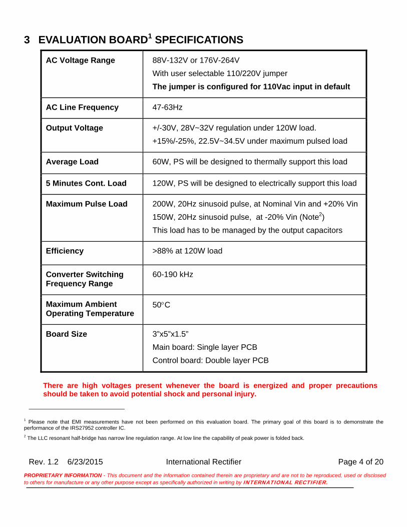
3 EVALUATION BOARD1 SPECIFICATIONS
AC Voltage Range 88V-132V or 176V-264V
With user selectable 110/220V jumper
The jumper is configured for 110Vac input in default
AC Line Frequency 47-63Hz
Output Voltage +/-30V, 28V~32V regulation under 120W load.
+15%/-25%, 22.5V~34.5V under maximum pulsed load
Average Load 60W, PS will be designed to thermally support this load
5 Minutes Cont. Load 120W, PS will be designed to electrically support this load
Maximum Pulse Load 200W, 20Hz sinusoid pulse, at Nominal Vin and +20% Vin
150W, 20Hz sinusoid pulse, at -20% Vin (Note2)
This load has to be managed by the output capacitors
Efficiency >88% at 120W load
Converter Switching Frequency Range
60-190 kHz
Maximum Ambient Operating Temperature
50C
Board Size 3”x5”x1.5”
Main board: Single layer PCB
Control board: Double layer PCB
There are high voltages present whenever the board is energized and proper precautions should be taken to avoid potential shock and personal injury.
1 Please note that EMI measurements have not been performed on this evaluation board. The primary goal of this board is to demonstrate the performance of the IRS27952 controller IC.
2 The LLC resonant half-bridge has narrow line regulation range. At low line the capability of peak power is folded back.
Rev. 1.2 6/23/2015 International Rectifier Page 5 of 20
PROPRIETARY INFORMATION - This document and the information contained therein are proprietary and are not to be reproduced, used or disclosed to others for manufacture or any other purpose except as specifically authorized in writing by INTERNATIONAL RECTIFIER.
3.1 Board Description
The evaluation board consists of a front-end AC-DC rectifier stage cascaded with a half-bridge resonant DC-
DC converter with +/-30V output voltage rails.
The front end is a conventional pi type EMI filter, followed by bridge rectifier stage. Two 200V/680uF bulk
capacitors are connected in series to provide stable DC bus voltage. The rectifier can be configured as full
bridge rectifier for 220Vac input, or voltage doubler rectifier for 110Vac input.
The downstream converter is a multi-resonant half bridge LLC converter whose control is implemented with the
IRS27952 controller HVIC (U101 on the control board). The controller drives the two half-bridge MOSFETs
with a 50 percent fixed duty cycle with pre-defined dead-time. Output voltage regulation is achieved by
changing the switching frequency according to the feedback signal.
IRS27952 is self-supplied in this reference design. The startup resistors R7 and R7A~C provide startup current
to IRS27952 during power up and charge the Vcc capacitors (CP3 and C5 on the main board). Once Vcc
voltage exceeds Vccuv+ threshold, IRS27952 starts operation and the auxiliary winding of power transformer
can provide bias to the IC. The voltage of auxiliary winding could vary a lot when load changes from 0A to full
load, so a linear regulator – Z101, R101 and Q101 (on the control board) – is used to keep Vcc regulated at
12V.
The transformer uses the magnetic integration approach, incorporating the resonant series and shunt
inductances in the power transformer. The transformer configuration chosen for the secondary winding is
center-tap. The feedback loop is implemented by means of a classical configuration using a TL431 (U104) to
adjust the current in the optocoupler PC817 (U103). The optocoupler transistor modulates the current from the
RT pin of the controller IC to modulate the switching frequency, thus achieving output voltage regulation.
The secondary side has two center-tapped windings for +30V and -30V output. Each rail has full wave rectifier
and filter with the return connected to center-tap. The feedback loop is configured to regulate the rail to rail
voltage to 60V. The balance of +30V and -30V is achieved by the symmetric windings of transformer.
Rev. 1.2 6/23/2015 International Rectifier Page 6 of 20
PROPRIETARY INFORMATION - This document and the information contained therein are proprietary and are not to be reproduced, used or disclosed to others for manufacture or any other purpose except as specifically authorized in writing by INTERNATIONAL RECTIFIER.
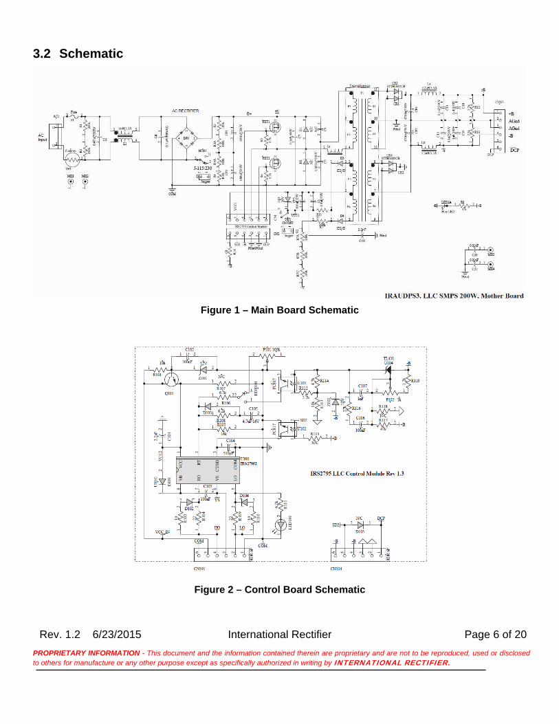
3.2 Schematic
Figure 1 – Main Board Schematic
Figure 2 – Control Board Schematic
Rev. 1.2 6/23/2015 International Rectifier Page 7 of 20
PROPRIETARY INFORMATION - This document and the information contained therein are proprietary and are not to be reproduced, used or disclosed to others for manufacture or any other purpose except as specifically authorized in writing by INTERNATIONAL RECTIFIER.
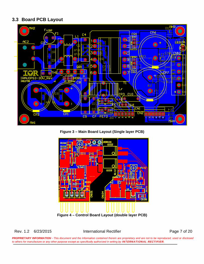
3.3 Board PCB Layout
Figure 3 – Main Board Layout (Single layer PCB)
Figure 4 – Control Board Layout (double layer PCB)
Rev. 1.2 6/23/2015 International Rectifier Page 8 of 20
PROPRIETARY INFORMATION - This document and the information contained therein are proprietary and are not to be reproduced, used or disclosed to others for manufacture or any other purpose except as specifically authorized in writing by INTERNATIONAL RECTIFIER.
3.4 Bill of Materials
Qty. Value Description Designator Digikey P/N Vendor
3 N/C C8, D1, D2
2 (open) MUR1620CTG (OPEN) CR1, CR2 (open) ON Semiconductor
1 2P AC Receptacle RA 2P AC Receptacle RA AC2 Q273-ND Qualtek
1 0.022uF/250V CAP .022UF 630V METAL POLYPRO C9 495-1329-ND EPCOS Inc
1 0.1uF/50V CAP .10UF 50V CERAMIC X7R 0805 C5 399-1169-1-ND Kemet
1 0.1uF/305VAC CAP .10UF 305VAC EMI SUPPRESSION C4 495-2319-ND EPCOS Inc
1 0.1uF/400V CAP .10UF 400V METAL POLY C7 495-2444-ND EPCOS Inc
2 0.1uF/100V CAP .1UF 100V CER X7R SMT 1206 C11, C14 399-1805-1-ND Kemet
1 0.47uF/305V CAP .47UF 305VAC EMI SUPPRESSION C3 495-2322-ND EPCOS Inc
1 100uF/25V CAP 100UF 25V ELECT VZ RADIAL CP3 493-1301-ND Nichicon
2 680uF/200V CAP 680UF 200V ELECT SMQ SNAP CP1, CP2 565-2733-ND United Chemi-Con
2 4700uF/50V CAPACITOR 4700UF 50V ELECT TSUP CP6, CP7 P6931-ND Panasonic - ECG
2 1uF/100V CAP CER 1UF 100V X7R 1206 C18, C19 490-3909-1-ND Murata Electronics North America
1 2.2nF CAP CER 2200PF 250VAC X1Y1 RAD C10 445-2411-ND TDK
2 0.01uF CAP CERM .01UF 10% 50V X7R 0805 C20, C21 478-1383-1-ND AVX Corporation
1 CONN BLOCK TERM PCB 5.08MM 6POS
CONN BLOCK TERM PCB 5.08MM 6POS CNN2 281-1438-ND Weidmuller
1 CONN HEADER 2POS .100 CONN HEADER 2POS .100 VERT TIN SW1 WM6602-ND
Molex Connector Corporation
1 3 pin header o.100" pitch CONN HEADER 3POS .100 VERT TIN HDR1 WM6603-ND
Molex Connector Corporation
2 STTH1002CB DIODE FAST 200V 10A D-PAK CR3, CR4 497-3536-5-ND STMicroelectronics
2 ES1D DIODE ULTRA FAST 1A 200V SMA D3, D4 ES1D-E3/61TGICT-ND
Vishay/General Semiconductor
1 24V DIODE ZENER 200MW 24V SOD323 DZ1 MMXZ5252B-TPMSCT-ND Micro Commercial Co
1 Transformer 019-7340-01R T1 Precision
1 Mini Fuse 4A FUSE 4A 250V 8.5X8.5 TIME-LAG Fuse 486-1474-ND Schurter Inc
1 Pico fuse holder FUSEHOLDER FOR SUB-MINI LINK PCB F1 486-1244-ND Schurter Inc
2 5.2uH/5.5A INDUCTOR POWER SHIELD 5.2UH SMD L4, L6 513-1396-1-ND
Cooper Bussmann, Copper Bussmann
1 Jumper Jumper Lr
2 IRS2795 Control Module IRS2795 Control Module CN1, CN2 IRS2795 IR-XIAN, IR_XIAN
1 Blue LED LED 470NM ROUND BLUE 3MM LED2A LED 470NM ROUND BLUE 3MM TT Electronics
1 1mH/2.2A LINE FILTER 1.0MH 2.2A N SERIES L1 PLK1076-ND Panasonic - ECG
4 Screw M3 MH-130 MH1, MH2, MH3, MH4
2 IPA50R250CP or FDPF18N50
MOSFET N-CH 550V 13A TO-220F or MOSFET N-CH 500V 18A TO-220F FET1, FET2
IPA50R250CP -ND FDPF18N50T-ND
Infineon / Fairchild
Rev. 1.2 6/23/2015 International Rectifier Page 9 of 20
PROPRIETARY INFORMATION - This document and the information contained therein are proprietary and are not to be reproduced, used or disclosed to others for manufacture or any other purpose except as specifically authorized in writing by INTERNATIONAL RECTIFIER.
1 GBU4J-BP RECT BRIDGE GPP 4A 600V GBU0 BR1 GBU4J-BPMS-ND Micro Commercial Co
1 0R RES 0 OHM 1/8W 0805 SMD R14 RHM0.0ARCT-ND Rohm Semiconductor
2 2.2k RES 2.2K OHM 1W 5% 2512 SMD R12, R13 PT2.2KXCT-ND Panasonic - ECG
2 4.7k RES 4.7K OHM 1/4W 5% 1206 SMD R5, R6 RHM4.7KERCT-ND Rohm Semiconductor
1 27 RES 27 OHM 1/4W 5% 1206 SMD R11 311-27ERCT-ND Yageo
1 47k RES 47K OHM 1/4W 5% 1206 SMD R8 RHM47KERCT-ND Rohm
8 100k RES 100K OHM 1/4W 5% 1206 SMD
R3, R3A, R4, R4A, R7, R7A, R7B, R7C RHM100KERCT-ND Rohm Semiconductor
2 220k RES 220K OHM 1/4W 5% 1206 SMD R1, R2 311-220KERCT-ND Yageo
2 Shorting Jumper Shorting Jumper 2P_HDR_.100 J1, J2 WM23944-ND Molex Connector Corporation
1 5 ohms TINRUSH CURRNT LMTR 5.0 OHM RADIAL TH1 495-2096-ND EPCOS Inc
BOM of Main Board
Qty. Value Description Designator Digikey P/N Vendor
1 2.2uF CAP CER 2.2UF 50V X7R 1206 C101 490-3367-1-ND Murata Electronics North America
1 100nF CAP .10UF 50V CERAMIC X7R 0805 C102 399-1169-1-ND Kemet
1 100nF CAP .10UF 50V CERAMIC X7R 1206 C103 399-1248-1-ND Kemet
1 510pF CAP CER 510PF 50V 5% C0G 0603 C104 490-1444-1-ND Kemet
1 4.7uF/16V CAP TANTALUM 4.7UF 16V 20% SMD C105 495-2233-1-ND Kemet
1 100nF CAP CER .1UF 50V 10% X7R 0603 C106 490-1519-1-ND Murata Electronics North America
1 1nF CAP 1000PF 50V CERAMICX7R 0603 C107 399-1082-1-ND Kemet
2 HDR 6P CONN HEADER 6POS .100 R/A TIN CN101, CN104 WM6006-ND
Molex Connector Corporation
1 US1G DIODE ULTRA FAST 1A 400V SMA D101 US1G-E3/61TGICT-ND
Vishay/General Semiconductor
2 SDM100K30L-7 DIODE SCHOTTKY 30V 1.0A SOD323 D102, D104 SDM100K30LDICT-ND Diodes Inc
1 1N4148WT-7 DIODE SWITCH 100V 150MW SOD-523 D103 1N4148WTDICT-ND Diodes Inc
1 N/C D105
1 3 pin header o.100" pitch CONN HEADER 3POS .100 VERT TIN HDR101 WM6603-ND
Molex Connector Corporation
1 Blue LED 468NM BLUE CLEAR 0805 SMD LED101 160-1645-1-ND Lite-On Inc
1 100k POT 1.0K OHM 3MM CERM SQ TOP SMD P101 ST32ETB104CT-ND Copal Electronics Inc
1 1k POT 1.0K OHM 3MM CERM SQ TOP SMD P102 ST32ETB102CT-ND Copal Electronics Inc
1 PBSS4350X TRANS NPN 50V 3A SOT89 Q101 568-4159-1-ND NXP Semiconductors
1 10k RES 10K OHM 1/10W 5% 0603 SMD R101 311-10KGRCT-ND Yageo
2 10 RES 10 OHM 1/8W 5% 0805 SMD R103, R110 P10ACT-ND Panasonic - ECG
2 22 RES 22 OHM 1/8W 5% 0805 SMD R104, R109 P22ACT-ND Panasonic - ECG
1 16k RES 16.0K OHM 1/10W 1% 0603 SMD R105 P16.0KHCT-ND Panasonic ECG
Rev. 1.2 6/23/2015 International Rectifier Page 10 of 20
PROPRIETARY INFORMATION - This document and the information contained therein are proprietary and are not to be reproduced, used or disclosed to others for manufacture or any other purpose except as specifically authorized in writing by INTERNATIONAL RECTIFIER.
3 6.2k RES 6.20K OHM 1/10W 1% 0603 SMD R106, R108, R111 P6.20KHCT-ND Panasonic ECG
3 N/C R107, R115, R118
1 2.7k RES 2.7K OHM 1/10W 5% 0603 SMD R112 311-2.7KGRCT-ND Yageo
1 10k RES 10K OHM 1/4W 5% 1206 SMD R113 RHM10KERCT-ND Rohm Semiconductor
1 4.7k RES 4.7K OHM 1/10W 5% 0603 SMD R114 311-4.7KGRCT-ND Yageo
1 27k RES 27.0K OHM 1/10W 1% 0603 SMD R116 311-27.0KHRCT-ND Yageo
1 47k RES 47.0K OHM 1/10W 1% 0603 SMD R117 311-47.0KHRCT-ND Yageo
1 1.2k RES 1.20K OHM 1/10W 1% 0603 SMD R119 311-1.20KHRCT-ND Yageo
1 IRS27952 IC DRIVER HALF BRIDGE OSC 8SOIC U101 IRS27952SPBF-ND
International Rectifier (Infineon Technologies)
2 PC817 PHOTOCOUPLER LO IF TRAN 4-SMD U102, U103 425-1461-1-ND Sharp Microelectronics
1 TL431 IC PREC SHUNT REG ADJ SOT23-3 U104 568-4883-1-ND NXP Semicondoctor
1 12V DIODE ZENER 200MW 12V SOD323 Z101 MM3Z12VT1GOSCT-ND ON Semiconductor
1 12V DIODE ZENER 500MW 12V SOD123 Z102 BZT52C12-FDICT-ND Diodes Inc
BOM of the Control Board
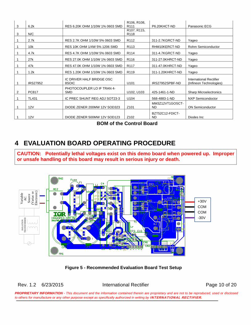
4 EVALUATION BOARD OPERATING PROCEDURE
CAUTION: Potentially lethal voltages exist on this demo board when powered up. Improper or unsafe handling of this board may result in serious injury or death.
Figure 5 - Recommended Evaluation Board Test Setup
IS
OLA
TIO
N
TRA
NSF
ORM
ER
AC
So
urce
(Var
iac
o r El
ectro
nic)
Var
iabl
e
+30V
COM
COM
-30V
Rev. 1.2 6/23/2015 International Rectifier Page 11 of 20
PROPRIETARY INFORMATION - This document and the information contained therein are proprietary and are not to be reproduced, used or disclosed to others for manufacture or any other purpose except as specifically authorized in writing by INTERNATIONAL RECTIFIER.
4.1 Load Connection
Connect electronic loads or class-D audio amplifier board (such as IRAUDAMP5) to connector CNN2. +30V is
marked as +B on the board, and -30V is marked as –B.
4.2 AC Input
The PSU is designed to work under narrow AC input range. On the main board there is a jumper to select AC
line voltage. If the jumper is shorted, the board works at 110Vac +/-20%. If the jumper is open, the board works
at 220Vac +/-20%.
The AC voltage select jumper HDR1 locates between the input bridge rectifier BR1 and Bus capacitor C8. The
default connection is for 110V AC input (HDR1 jumper is shorted).
An isolation transformer on the AC side is highly recommended, so that all the control signals on the board can
easily be probed by using regular scope probes.
The NTC resistor limits the inrush current upon initial application of full AC line voltage. Once power is applied
to demo board, potentially lethal high voltages will be present on board and necessary precautions should be
taken to avoid serious injury.
4.3 IRS27952 DC Supply Voltage
The board is self-supplied by startup circuit and auxiliary winding of transformer. The startup circuit starts to
work once AC or DC input voltage applies to the board.
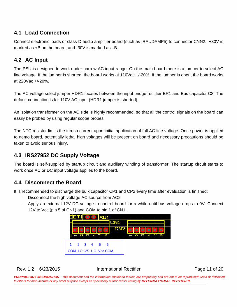
4.4 Disconnect the Board
It is recommended to discharge the bulk capacitor CP1 and CP2 every time after evaluation is finished:
- Disconnect the high voltage AC source from AC2
- Apply an external 12V DC voltage to control board for a while until bus voltage drops to 0V. Connect
12V to Vcc (pin 5 of CN1) and COM to pin 1 of CN1.
1 2 3 4 5 6
COM LO VS HO Vcc COM
Rev. 1.2 6/23/2015 International Rectifier Page 12 of 20
PROPRIETARY INFORMATION - This document and the information contained therein are proprietary and are not to be reproduced, used or disclosed to others for manufacture or any other purpose except as specifically authorized in writing by INTERNATIONAL RECTIFIER.
5 SYSTEM PERFORMANCE CHARACTERIZATION
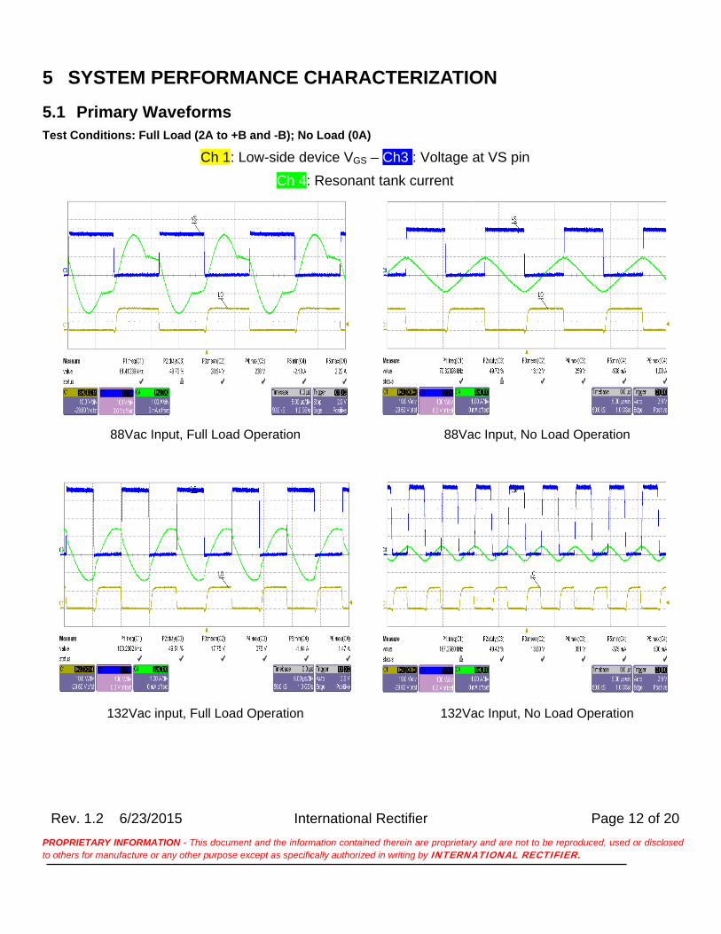
5.1 Primary Waveforms Test Conditions: Full Load (2A to +B and -B); No Load (0A)
Ch 1: Low-side device VGS – Ch3 : Voltage at VS pin
Ch 4: Resonant tank current
88Vac Input, Full Load Operation 88Vac Input, No Load Operation
132Vac input, Full Load Operation 132Vac Input, No Load Operation
Rev. 1.2 6/23/2015 International Rectifier Page 13 of 20
PROPRIETARY INFORMATION - This document and the information contained therein are proprietary and are not to be reproduced, used or disclosed to others for manufacture or any other purpose except as specifically authorized in writing by INTERNATIONAL RECTIFIER.
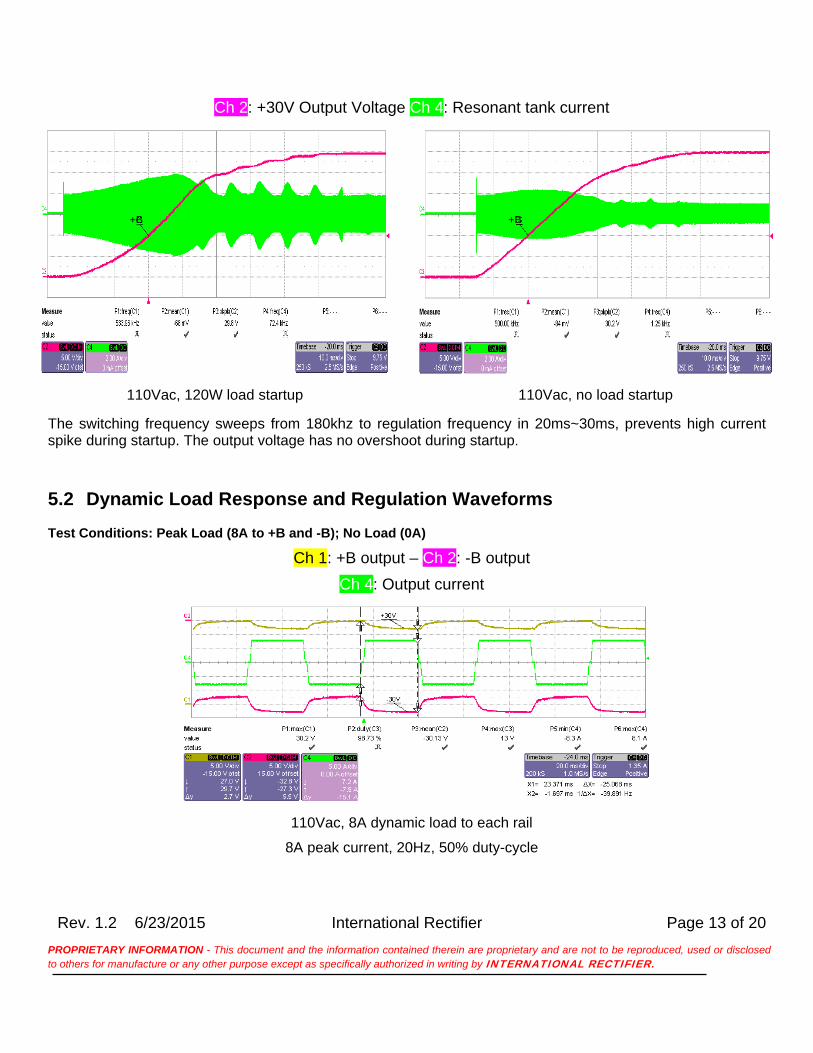
Ch 2: +30V Output Voltage Ch 4: Resonant tank current
110Vac, 120W load startup 110Vac, no load startup
The switching frequency sweeps from 180khz to regulation frequency in 20ms~30ms, prevents high current spike during startup. The output voltage has no overshoot during startup.
5.2 Dynamic Load Response and Regulation Waveforms
Test Conditions: Peak Load (8A to +B and -B); No Load (0A)
Ch 1: +B output – Ch 2: -B output
Ch 4: Output current
110Vac, 8A dynamic load to each rail
8A peak current, 20Hz, 50% duty-cycle
+B +B
Rev. 1.2 6/23/2015 International Rectifier Page 14 of 20
PROPRIETARY INFORMATION - This document and the information contained therein are proprietary and are not to be reproduced, used or disclosed to others for manufacture or any other purpose except as specifically authorized in writing by INTERNATIONAL RECTIFIER.
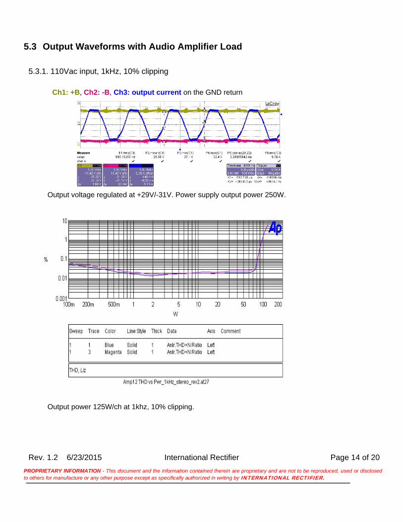
5.3 Output Waveforms with Audio Amplifier Load
5.3.1. 110Vac input, 1kHz, 10% clipping
Ch1: +B, Ch2: -B, Ch3: output current on the GND return
Output voltage regulated at +29V/-31V. Power supply output power 250W.
Output power 125W/ch at 1khz, 10% clipping.
Rev. 1.2 6/23/2015 International Rectifier Page 15 of 20
PROPRIETARY INFORMATION - This document and the information contained therein are proprietary and are not to be reproduced, used or disclosed to others for manufacture or any other purpose except as specifically authorized in writing by INTERNATIONAL RECTIFIER.
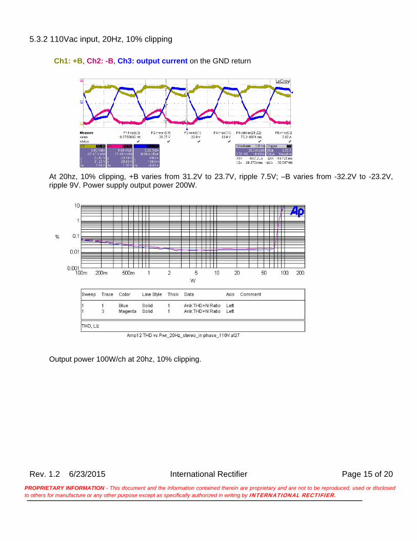
5.3.2 110Vac input, 20Hz, 10% clipping
Ch1: +B, Ch2: -B, Ch3: output current on the GND return
At 20hz, 10% clipping, +B varies from 31.2V to 23.7V, ripple 7.5V; –B varies from -32.2V to -23.2V, ripple 9V. Power supply output power 200W.
Output power 100W/ch at 20hz, 10% clipping.
Rev. 1.2 6/23/2015 International Rectifier Page 16 of 20
PROPRIETARY INFORMATION - This document and the information contained therein are proprietary and are not to be reproduced, used or disclosed to others for manufacture or any other purpose except as specifically authorized in writing by INTERNATIONAL RECTIFIER.
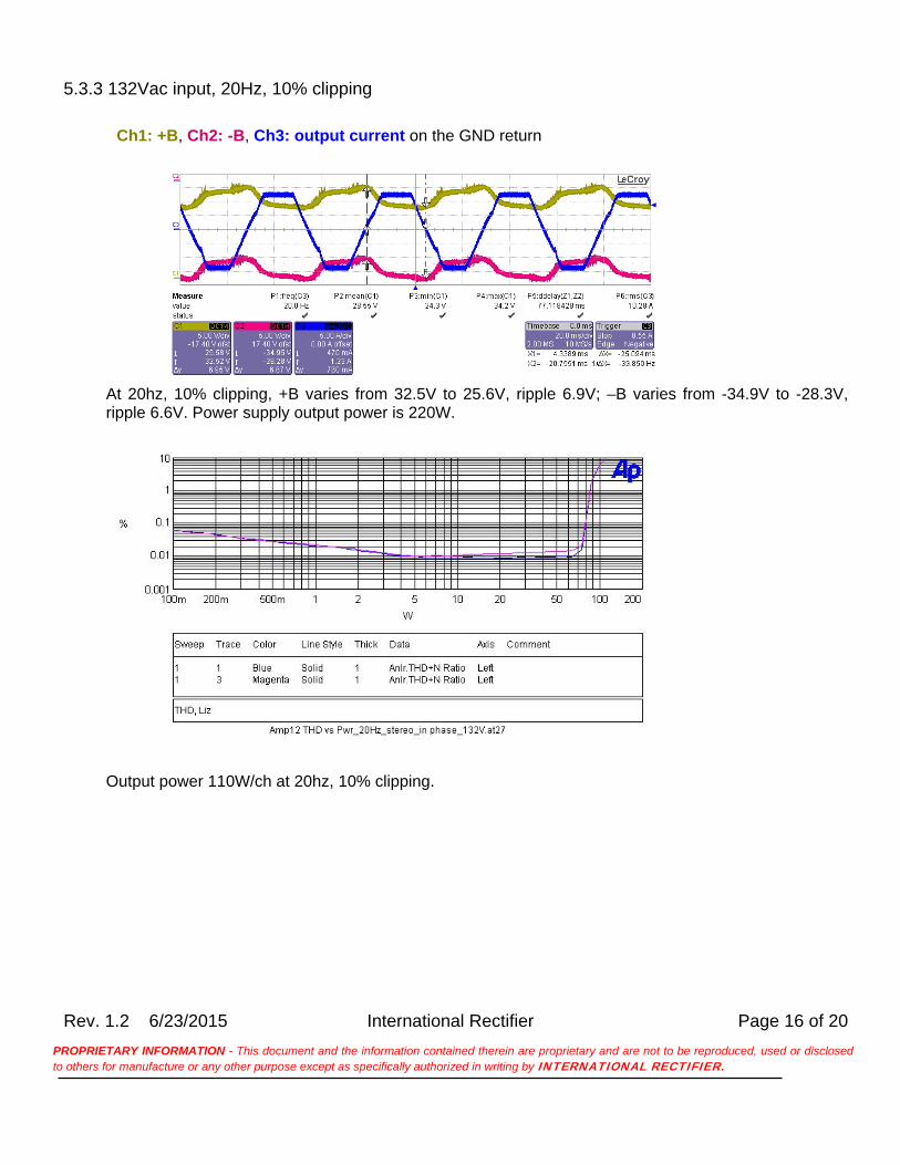
5.3.3 132Vac input, 20Hz, 10% clipping
Ch1: +B, Ch2: -B, Ch3: output current on the GND return
At 20hz, 10% clipping, +B varies from 32.5V to 25.6V, ripple 6.9V; –B varies from -34.9V to -28.3V, ripple 6.6V. Power supply output power is 220W.
Output power 110W/ch at 20hz, 10% clipping.
Rev. 1.2 6/23/2015 International Rectifier Page 17 of 20
PROPRIETARY INFORMATION - This document and the information contained therein are proprietary and are not to be reproduced, used or disclosed to others for manufacture or any other purpose except as specifically authorized in writing by INTERNATIONAL RECTIFIER.
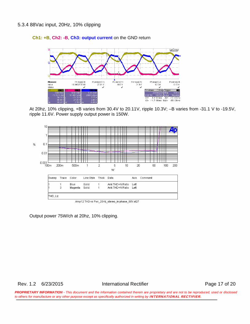
5.3.4 88Vac input, 20Hz, 10% clipping
Ch1: +B, Ch2: -B, Ch3: output current on the GND return
At 20hz, 10% clipping, +B varies from 30.4V to 20.11V, ripple 10.3V; –B varies from -31.1 V to -19.5V, ripple 11.6V. Power supply output power is 150W.
Output power 75W/ch at 20hz, 10% clipping.
Rev. 1.2 6/23/2015 International Rectifier Page 18 of 20
PROPRIETARY INFORMATION - This document and the information contained therein are proprietary and are not to be reproduced, used or disclosed to others for manufacture or any other purpose except as specifically authorized in writing by INTERNATIONAL RECTIFIER.
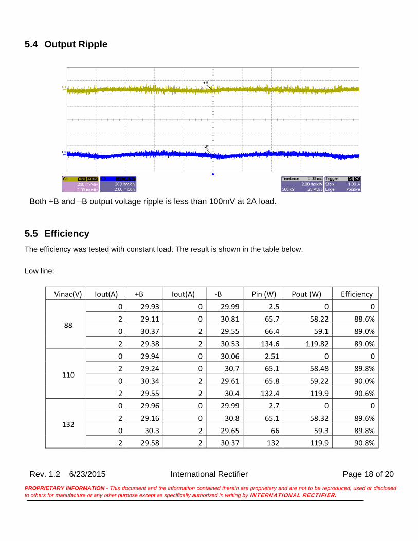
5.4 Output Ripple
Both +B and –B output voltage ripple is less than 100mV at 2A load.
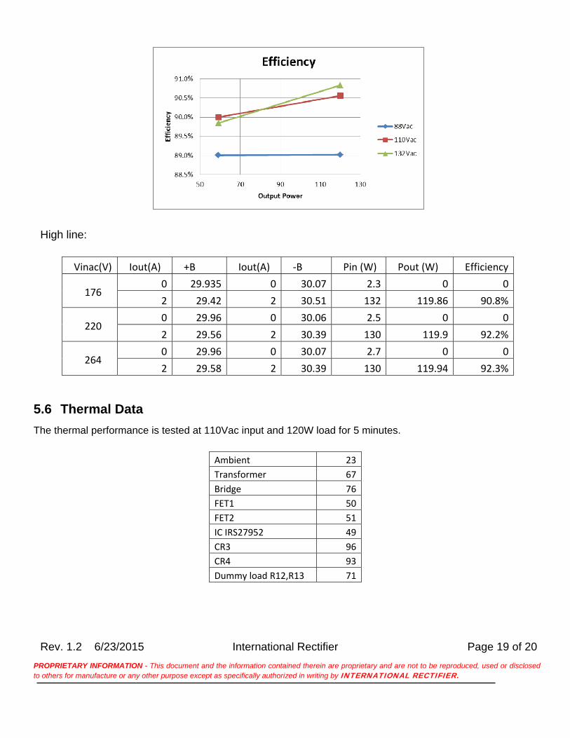
5.5 Efficiency
The efficiency was tested with constant load. The result is shown in the table below.
Low line:
Vinac(V) Iout(A) +B Iout(A) ‐B Pin (W) Pout (W) Efficiency
88
0 29.93 0 29.99 2.5 0 0
2 29.11 0 30.81 65.7 58.22 88.6%
0 30.37 2 29.55 66.4 59.1 89.0%
2 29.38 2 30.53 134.6 119.82 89.0%
110
0 29.94 0 30.06 2.51 0 0
2 29.24 0 30.7 65.1 58.48 89.8%
0 30.34 2 29.61 65.8 59.22 90.0%
2 29.55 2 30.4 132.4 119.9 90.6%
132
0 29.96 0 29.99 2.7 0 0
2 29.16 0 30.8 65.1 58.32 89.6%
0 30.3 2 29.65 66 59.3 89.8%
2 29.58 2 30.37 132 119.9 90.8%
Rev. 1.2 6/23/2015 International Rectifier Page 19 of 20
PROPRIETARY INFORMATION - This document and the information contained therein are proprietary and are not to be reproduced, used or disclosed to others for manufacture or any other purpose except as specifically authorized in writing by INTERNATIONAL RECTIFIER.
High line:
Vinac(V) Iout(A) +B Iout(A) ‐B Pin (W) Pout (W) Efficiency
176 0 29.935 0 30.07 2.3 0 0
2 29.42 2 30.51 132 119.86 90.8%
220 0 29.96 0 30.06 2.5 0 0
2 29.56 2 30.39 130 119.9 92.2%
264 0 29.96 0 30.07 2.7 0 0
2 29.58 2 30.39 130 119.94 92.3%
5.6 Thermal Data
The thermal performance is tested at 110Vac input and 120W load for 5 minutes.
Ambient 23
Transformer 67
Bridge 76
FET1 50
FET2 51
IC IRS27952 49
CR3 96
CR4 93
Dummy load R12,R13 71
Rev. 1.2 6/23/2015 International Rectifier Page 20 of 20
PROPRIETARY INFORMATION - This document and the information contained therein are proprietary and are not to be reproduced, used or disclosed to others for manufacture or any other purpose except as specifically authorized in writing by INTERNATIONAL RECTIFIER.
6 Transformer Spec Minimum operating frequency: 60 kHz
Minimum operating frequency: 200 kHz
Primary inductance: 600 µH 10% @1 kHz - 0.25V (Note 1)
Leakage inductance: 160 µH 10% @1 kHz - 0.25V (Note 2)
Note: 1 Measured between Pins 4 and 6
Note: 2 Measured between Pins 4 and 6 with secondary windings shorted
6.1 Electrical Diagram
5
3
1
P2
P3
6
4
2
6
5
4
P1
P4
9
7
8
8
10
12
P3, P4
NC
1
S4
S1
11
7
9
11
Primarywinding (P1, P2)
Bottom View
3
2
S3
12S2
10
IRAUDPS3 transformer
Secondary windings S1,S2 S3, S4
Schematic
e
Transformer cross section view winding's sequencing
6.2 Resonant Transformer Winding Characteristics
Winding Pins Turn number RMS Current
P1&P2 4 - 6 58 1.5A
P3 1 -2 4 0.1A
P4 2 -3 4 0.1A
S1 11 - 10 10 1.6A
S2 10 – 12 10 1.6A
S3 8 - 7 10 1.6A
S4 7- 9 10 1.6A