ion implantation - dspace.mit.edu...ion velocity=> charge separation, drag passing ion causes...
TRANSCRIPT
ION IMPLANTATION
We saw how dopants were introduced into a wafer by using diffusion(‘predeposition’ and ‘drive-in’).
This process is limited:
-cannot exceed solid solubility of dopant
-difficult to achieve light doping
Ion implantation is preferred because:
-controlled, low or high dose can be introduced (1011 - 1018 cm-2)
-depth of implant can be controlled.
Used since 1980, despite substrate damage;
low throughput, and cost.
Plummer Ch. 8, Campbell Ch. 5
3.155J/6.152J, 2003 1
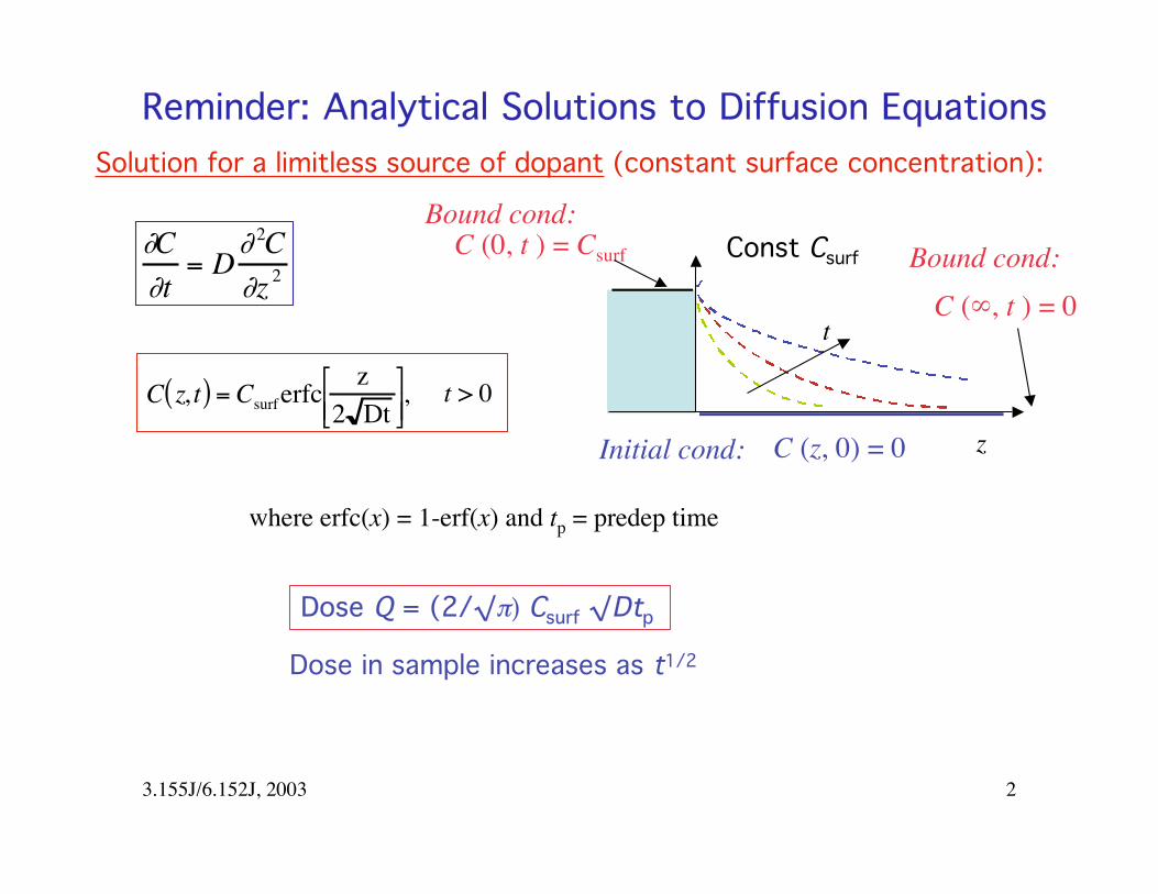
Reminder: Analytical Solutions to Diffusion Equations
Solution for a limitless source of dopant (constant surface concentration):
Bound cond:∂C
= D∂ 2C C (0, t ) = Csurf
C (∞, t ) = 0 t
Bound cond: Const Csurf
∂t ∂z 2
È z ˘(C z, t) = Csurf erfcÍ2 Dt , t > 0
ÎzInitial cond: C (z, 0) = 0
where erfc(x) = 1-erf(x) and tp = predep time
Dose Q = (2/√p) Csurf √Dtp
Dose in sample increases as t1/2
3.155J/6.152J, 2003 2
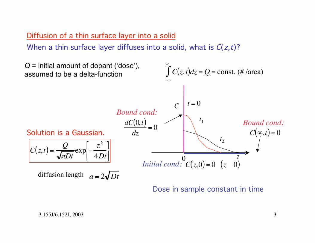
Diffusion of a thin surface layer into a solid
When a thin surface layer diffuses into a solid, what is C(z,t)?
Q = initial amount of dopant (‘dose’), •
Ú C z, t)dz = Q = const. (# /area) assumed to be a delta-function ( -•
t1
t2
t = 0C Bound cond:
dC(0, t) Bound cond: = 0
C(•,t) = 0Solution is a Gaussian. dz 2Q È z ˘
(C z, t) = exp -pDt ÎÍ 4 Dt˚ z0
(Initial cond: C z,0) = 0 ( z ≠ 0)diffusion length a = 2 Dt
Dose in sample constant in time
3.155J/6.152J, 2003 3
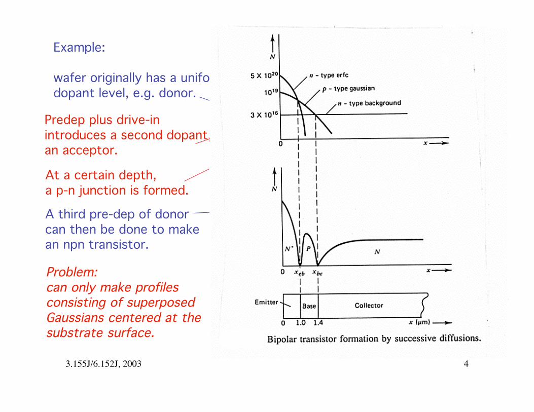
Example:
wafer originally has a uniformdopant level, e.g. donor.
Predep plus drive-in introduces a second dopant, an acceptor.
At a certain depth, a p-n junction is formed.
A third pre-dep of donor can then be done to make an npn transistor.
Problem: can only make profiles consisting of superposed Gaussians centered at the substrate surface.
3.155J/6.152J, 2003 4
Since the maximum amount of a dopant that can dissolve in the Si is given by the solid solubility, you may be limited in the amount of dopant that can be incorporated.
3.155J/6.152J, 2003 5
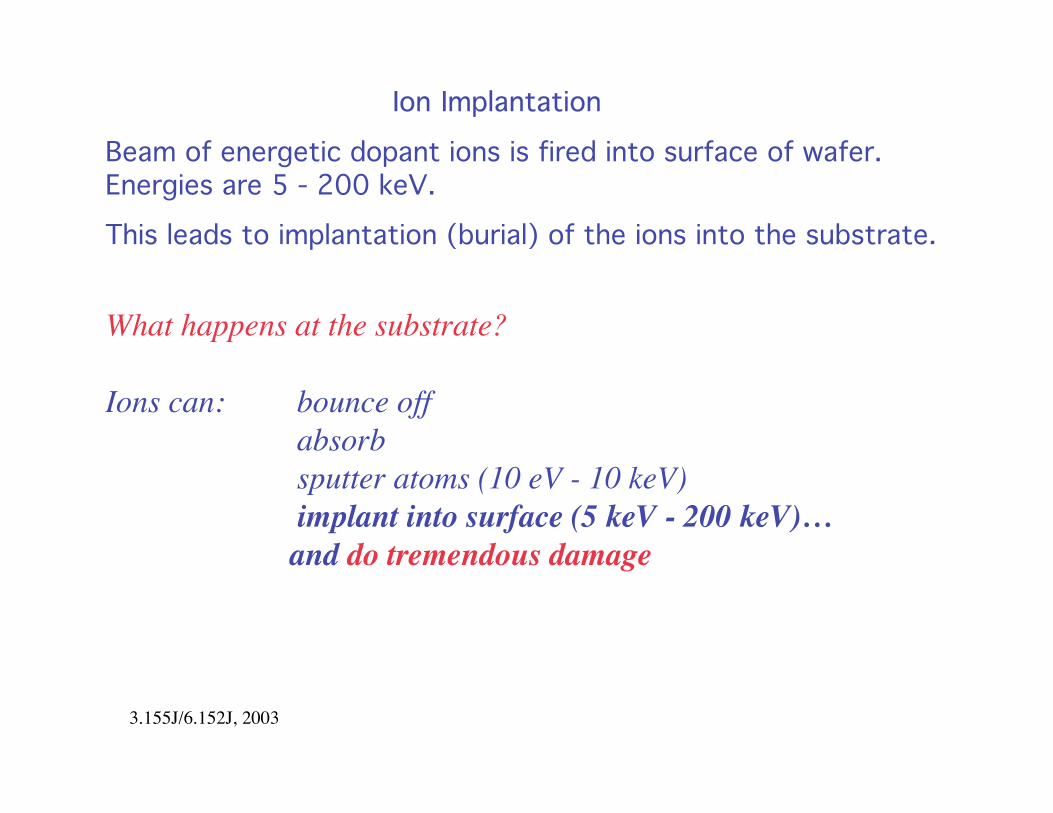
Ion Implantation
Beam of energetic dopant ions is fired into surface of wafer. Energies are 5 - 200 keV.
This leads to implantation (burial) of the ions into the substrate.
What happens at the substrate?
Ions can: bounce off absorb sputter atoms (10 eV - 10 keV) implant into surface (5 keV - 200 keV)… and do tremendous damage
3.155J/6.152J, 2003
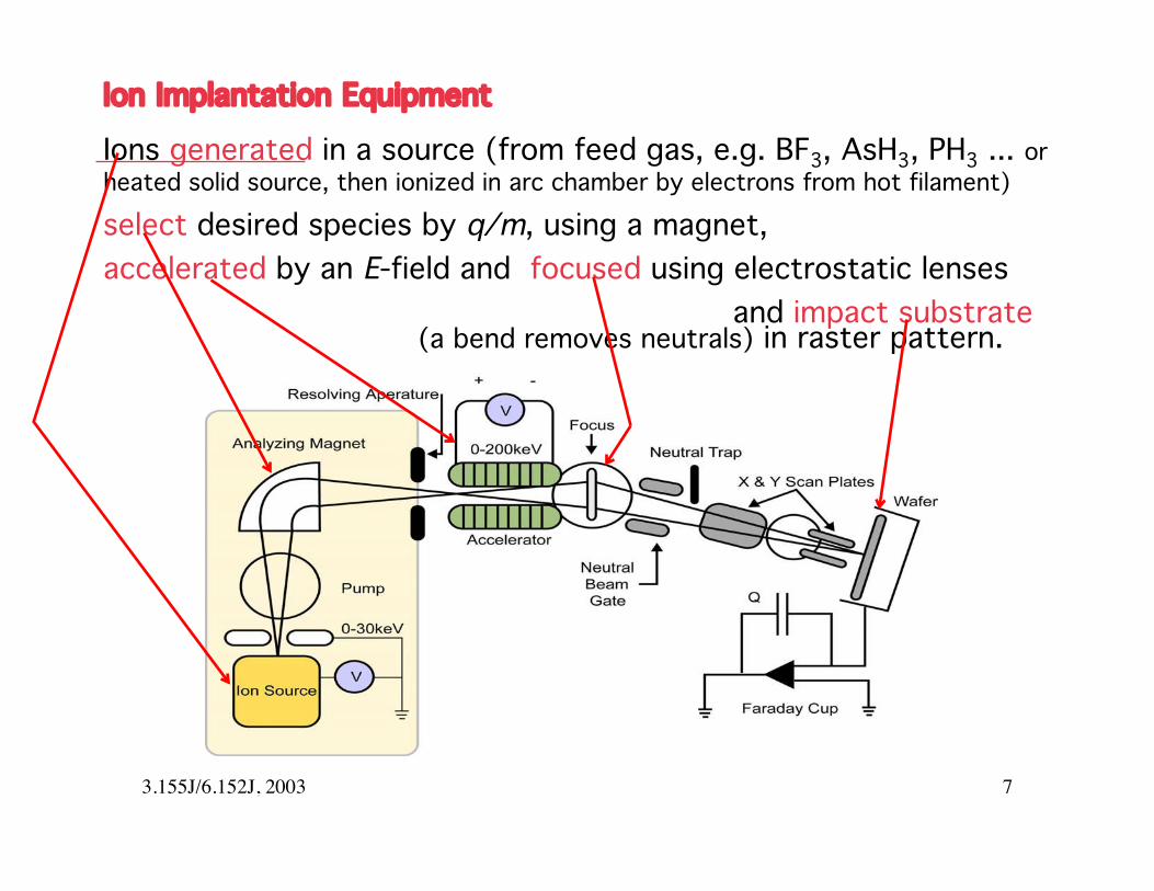
Ion Implantation Equipment
Ions generated in a source (from feed gas, e.g. BF3, AsH3, PH3 ... orheated solid source, then ionized in arc chamber by electrons from hot filament)
select desired species by q/m, using a magnet, accelerated by an E-field and focused using electrostatic lenses
and impact substrate(a bend removes neutrals) in raster pattern.
3.155J/6.152J, 2003 7
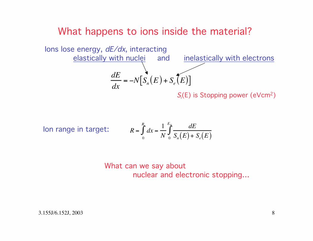
What happens to ions inside the material?
Ions lose energy, dE/dx, interacting elastically with nuclei and inelastically with electrons
dE = -N S (E ) + S (E)][ ndx e
S (E) is Stopping power (eVcm2)i
R 0 dEIon range in target: R = Ú dx = 1 E
ÚN 0 S (E) + S (E )0 n e
What can we say about nuclear and electronic stopping…
3.155J/6.152J, 2003 8
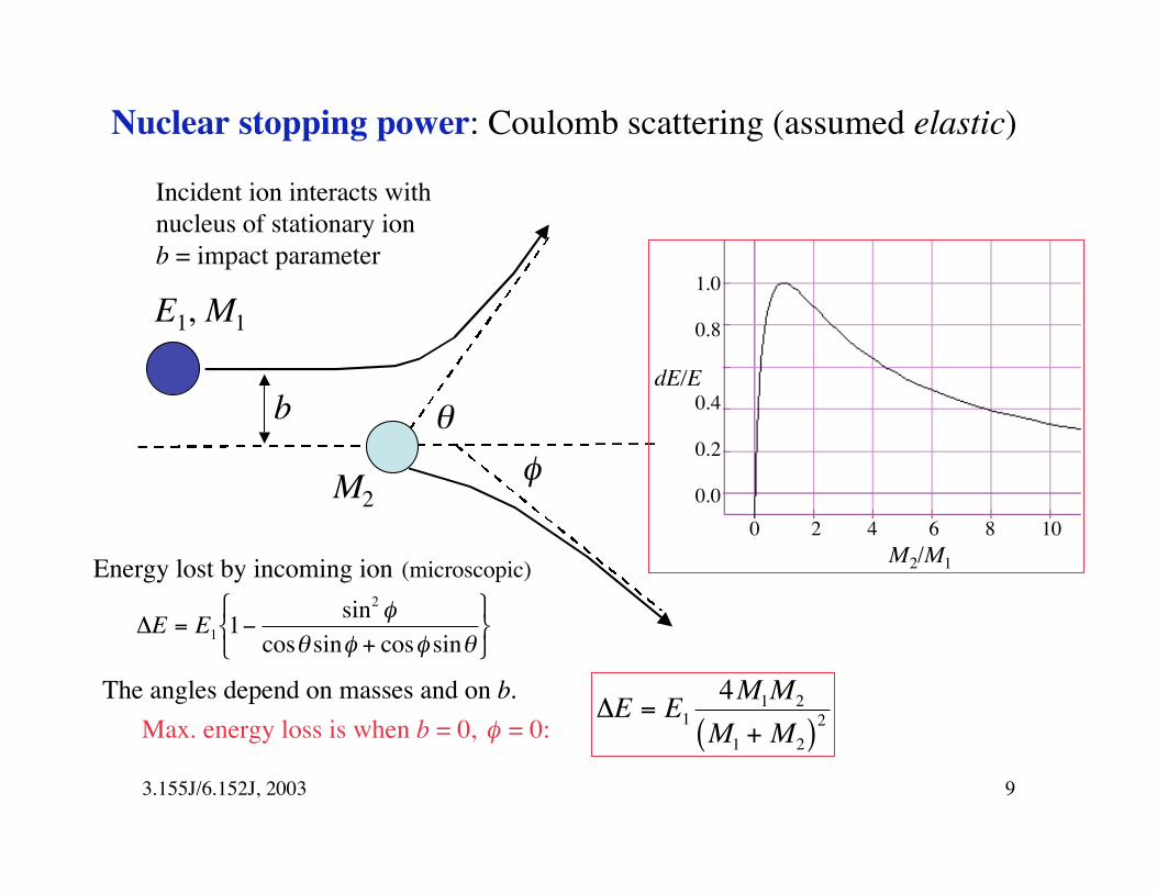
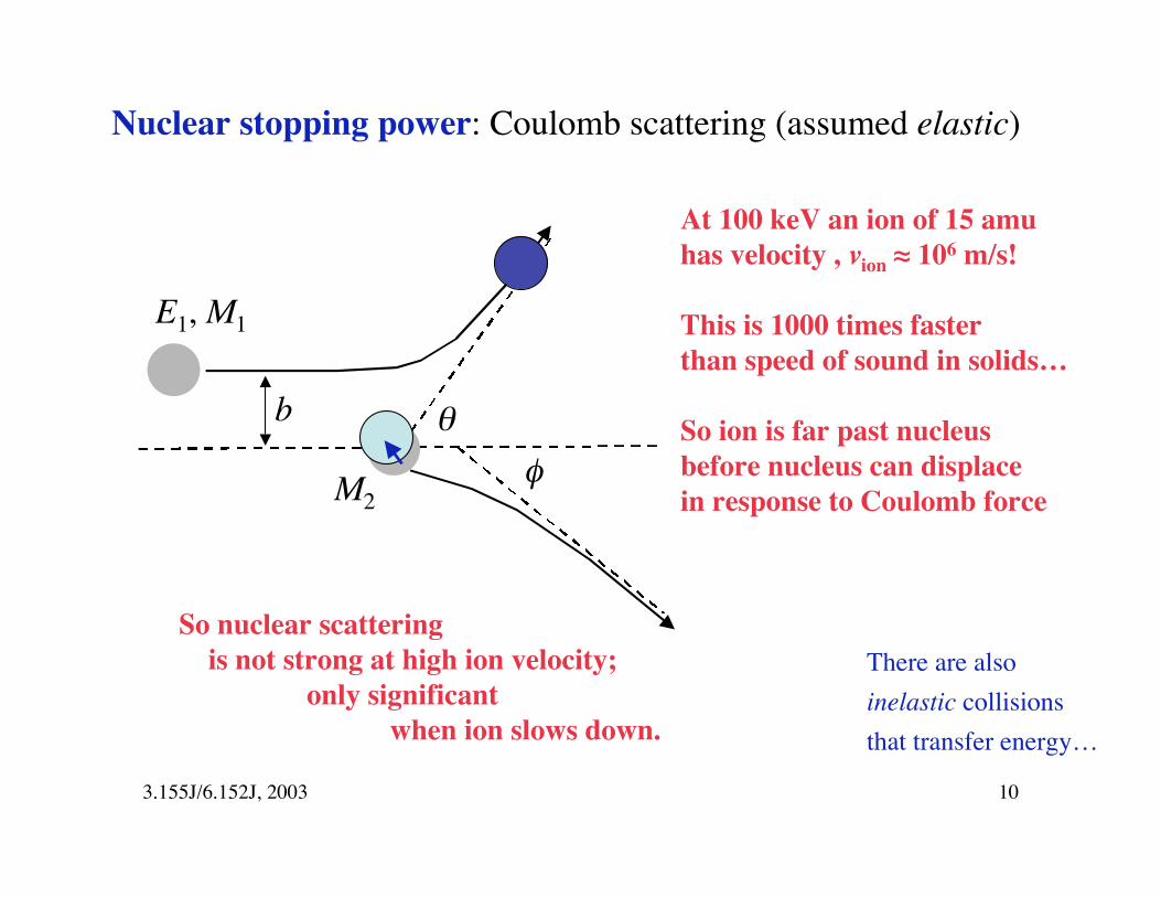
Nuclear stopping power: Coulomb scattering (assumed elastic)
Incident ion interacts with
b
q
f
b
E1, M1
M2
Energy lost by incoming ion (microscopic)
DE = E1 1 -sin2 f
cosq sinf + cosf sinq
Ï Ì Ó
¸ ˝ ˛
0 2 4 6 8 10 M2/M1
1.0
0.8
dE/E 0.4
0.2
0.0
nucleus of stationary ion = impact parameter
The angles depend on masses and on b.
Max. energy loss is when b = 0, f = 0:
4 M1M2DE = E1 (M1 + M2 )
2
3.155J/6.152J, 2003 9
q
f
b
E1, M1
M2
q
f
b
E1, M1
M2
F µQ1Q2
r2
Nuclear stopping power: Coulomb scattering (assumed elastic)
q
f
b
E1, M1
M2
So nuclear scattering
At 100 keV an ion of 15 amu has velocity , vion ≈ 106 m/s!
This is 1000 times faster than speed of sound in solids…
So ion is far past nucleus before nucleus can displace in response to Coulomb force
is not strong at high ion velocity; There are also only significant inelastic collisions
when ion slows down. that transfer energy…
3.155J/6.152J, 2003 10
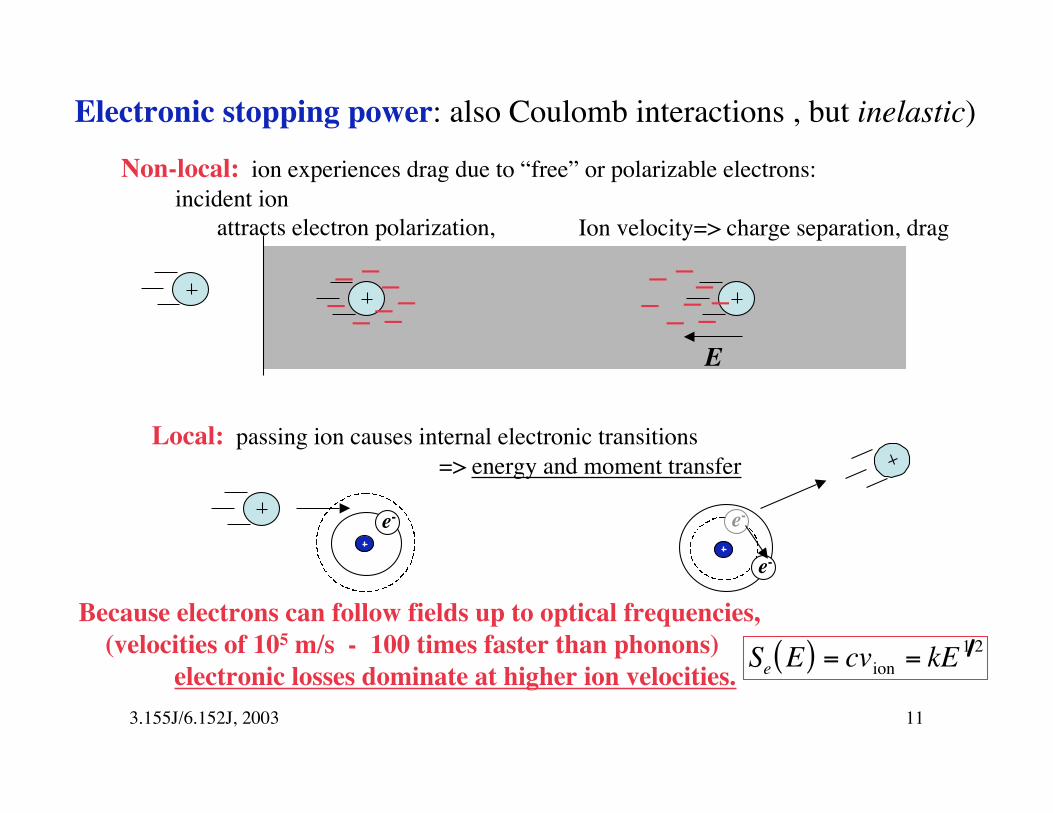
Electronic stopping power: also Coulomb interactions , but inelastic)
Non-local: ion experiences drag due to “free” or polarizable electrons:incident ion
attracts electron polarization,
Local: => energy and moment transfer
E
e -
e -
e -
Ion velocity=> charge separation, drag
passing ion causes internal electronic transitions
Because electrons can follow fields up to optical frequencies, (velocities of 105 m/s - 100 times faster than phonons) S ( E) = cvioneelectronic losses dominate at higher ion velocities.
3.155J/6.152J, 2003 11
= kE 1 2
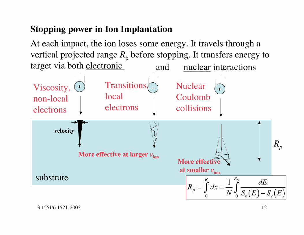
Stopping power in Ion Implantation
At each impact, the ion loses some energy. It travels through a vertical projected range Rp before stopping. It transfers energy to target via both electronic and nuclear interactions
Transitions, NuclearViscosity, local Coulombnon-local electrons collisionselectrons
substrate
velocity
More effective at larger vion More effective at smaller vion
Rp
Rp = dx 0
R
Ú = 1
N
dE
Sn E( ) + Se E( )0
E0
Ú
3.155J/6.152J, 2003 12
tt
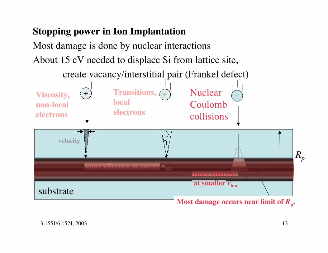
Stopping power in Ion Implantation
Most damage is done by nuclear interactions
About 15 eV needed to displace Si from lattice site,
create vacancy/interstitial pair (Frankel defect)
Transitions, NuclearViscosity,non-local local Coulombelectrons electrons collisions
R
substrate
velocity
More effective at smaller vion
More effective at larger vion
Rp.
ff iM i lff iMM i lMM t lMM t lM t l vlarger vat larger vvat larger vvat larger vvat larger vvat larger vvat larger vviat larger vviat larger viviat larger vivionat larger viMore effective at larger vionat larger viong iong iong iong iong iong iong iong iong iong ionionionionionff iM iff iMM iMMMM eMMore effecti eMore effectiveMore effectiveMore effectiveMore effectiveMore effectiveMore effectiveMore effectiveMore effectiveMore effectiveMore effectiveMore effectiveMore effectivellllttt
Most damage occurs near limit of
More effectiMore effecti e atMore effectiveMore effectiveMore effectiveMore effectiveMore effectiveMore effectiveMore effectiveMore effectiveMore effectiveMore effectiveMore effectivetititiffff ti t lffff ti t lffff ti t lff e at largerffMore effective at largerMore effective at largerMore effective at largerMore effective at largerMore effective at largerMore effective at largerMore effective at largerMore effective at largerMore effective at largerMore effective at largerMore effective at largerffff tiffff tiff tiff tiff tiMore effectiff tiMore effectiveMore effectiveMore effectiveMore effectiveMore effectiveMore effectiveMore effectiveMore effectiveMore effectiveMore effectiveMore effectivellllllllll
p
3.155J/6.152J, 2003 13
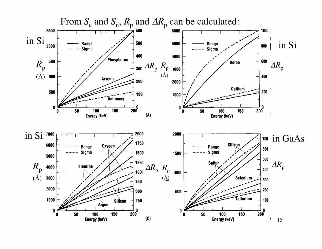
3.155J/6.152J, 2003 15
From Se and Sn, Rp and DRp
Rp DRp
in Si in Si
in Si in GaAs
DRp Rp
Rp (Å)
DRp
DRpRp (Å)
can be calculated:
(Å)
(Å)
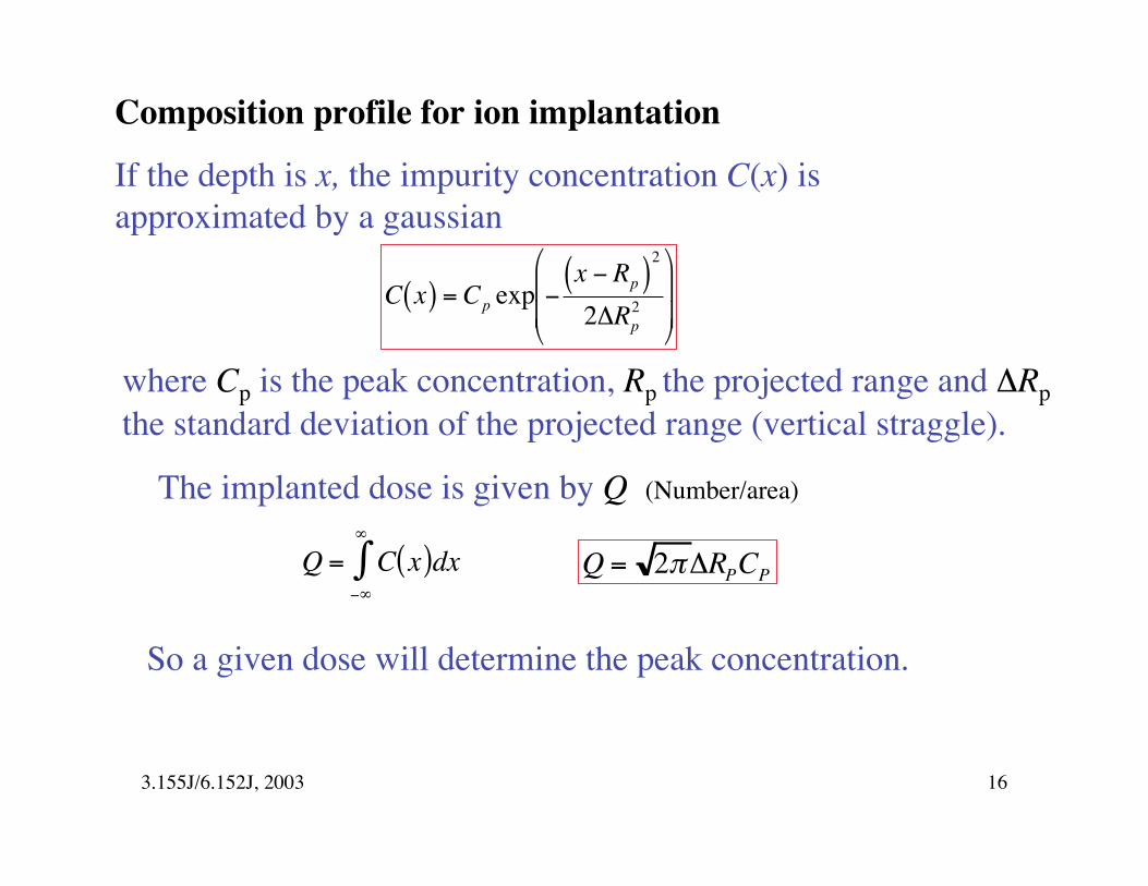
Composition profile for ion implantation
If the depth is x, the impurity concentration C(x) is approximated by a gaussian
Ê
C x) = Cp expÁ-(x - Rp )
2 ˆ
(Á 2DR2 ˜
˜
pË ¯
where Cp is the peak concentration, Rp the projected range and DRp
the standard deviation of the projected range (vertical straggle).
The implanted dose is given by Q (Number/area)
•
(Q = Ú C x)dx -•
Q = 2pDRP CP
So a given dose will determine the peak concentration.
3.155J/6.152J, 2003 16
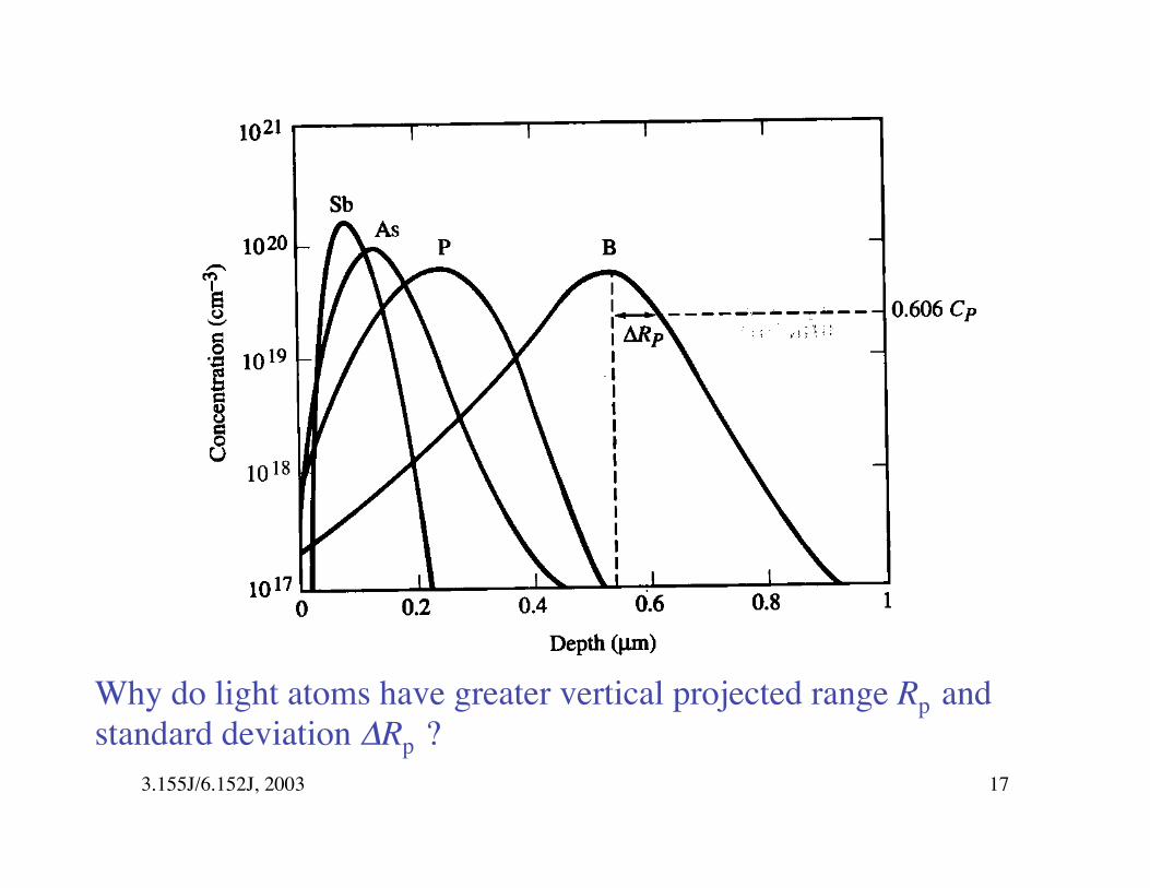
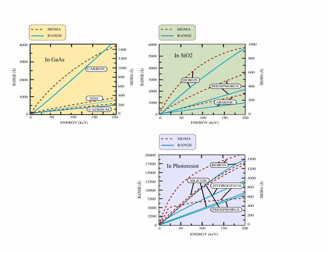
200 keV implants in Si
Why do light atoms have greater vertical projected range Rp and standard deviation DR ?p
3.155J/6.152J, 2003 17
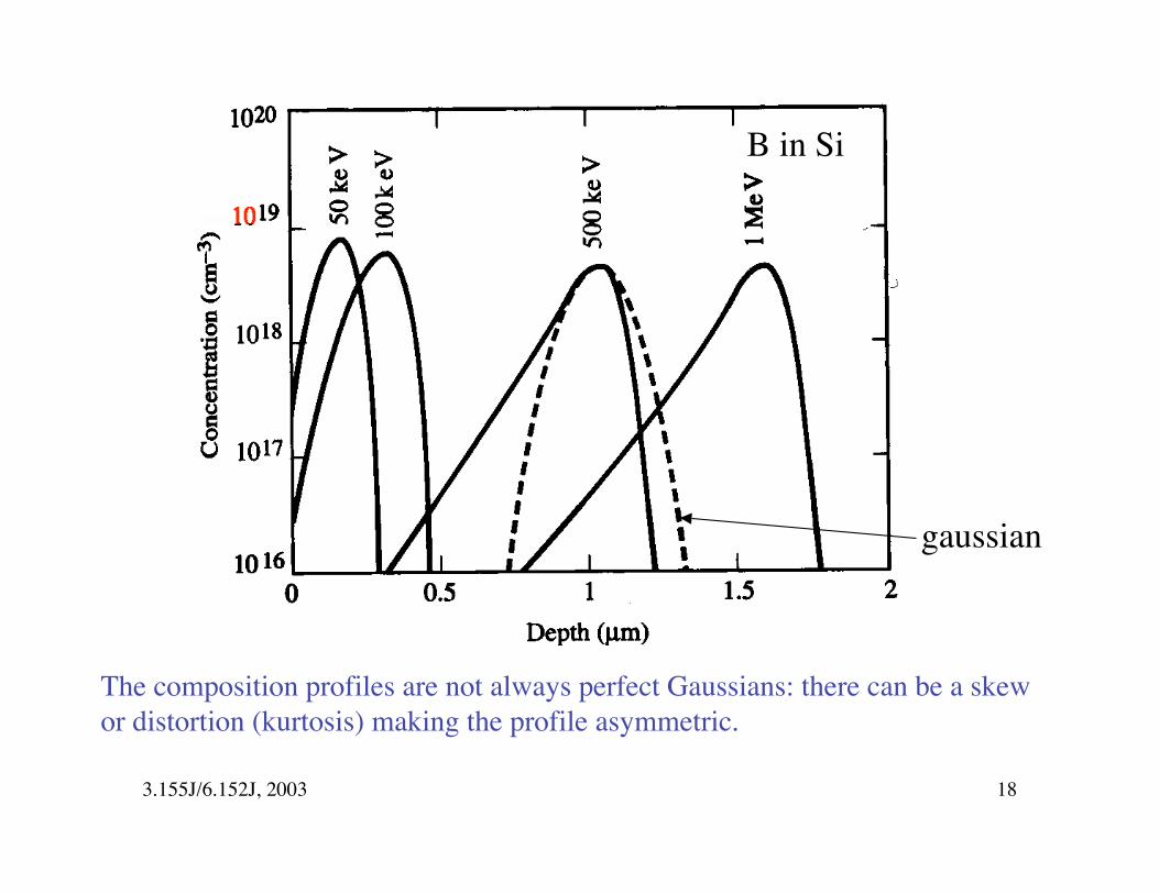
B in Si
gaussian
The composition profiles are not always perfect Gaussians: there can be a skew or distortion (kurtosis) making the profile asymmetric.
3.155J/6.152J, 2003 18
Channeling
If the ions are incident parallel to a major crystal direction, they can pass through the structure with less scattering, so the range is much larger than expected.
3.155J/6.152J, 2003 19
Nuclear Stopping
Need to sum the effects of all the scattering events, e.g. using Monte Carlomodeling. Nuclear stopping, Sn, can bemodeled by Coulomb scattering (so it depends on impact parameter, relative masses, and E).
3.155J/6.152J, 2003 20
ModelingDistributions of ions after implant can be modeled using a Monte Carlo calculation to give projected range. Can include both nuclear and electronic stopping Ion implantation can be modeled using SUPREM, which calculates dopant profiles vs. implant conditions and annealing.
3.155J/6.152J, 2003 21
P
* ˆÊCP* * *2ln ÁÁ ˜ = RPxm = RP + DRP ËCB ¯
xm = range + some multiple, m, of std dev’n
Dose penetrating mask: ˆ2˘
˙QP = Q Ú
•
expÍÍÈ
-ÁÁÊ x - RP
*
˜ * ˜ dx
2pDRP *
Î Ë 2DRP ¯ ˚x m
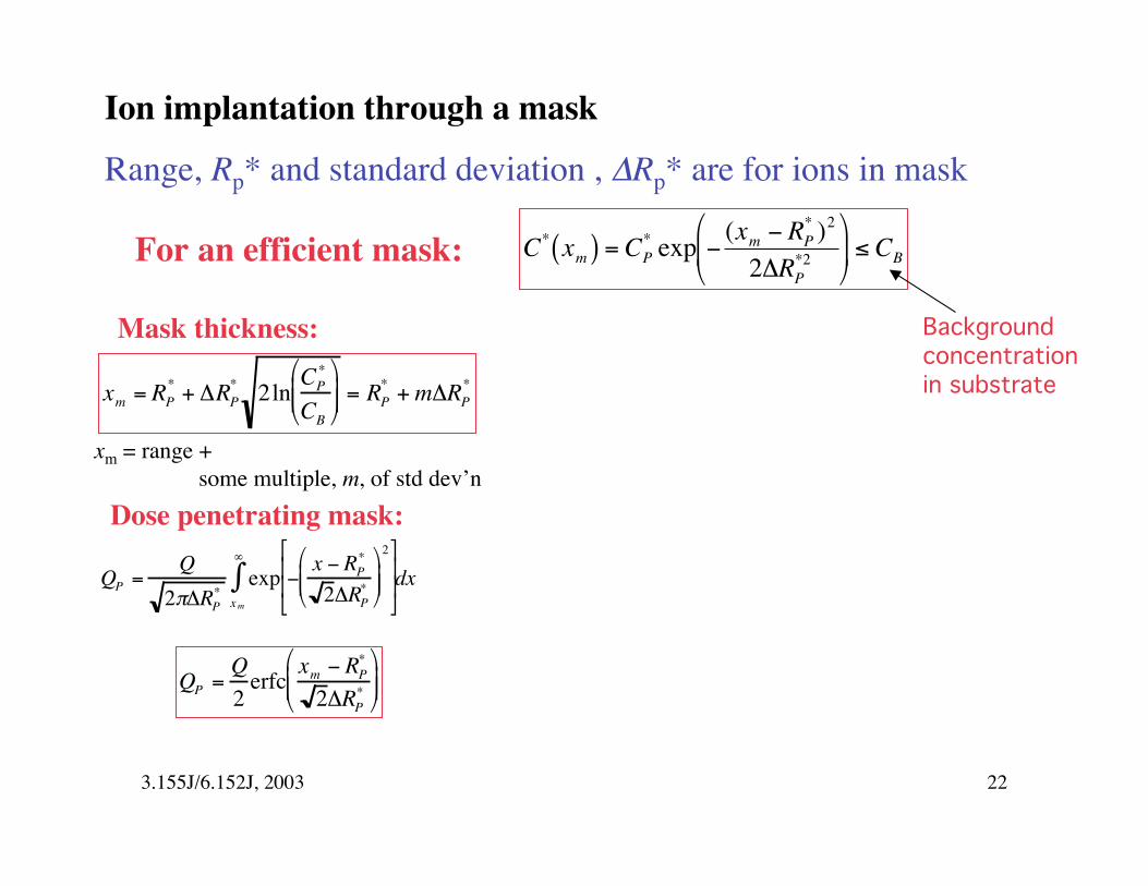
Ion implantation through a mask
Range, Rp* and standard deviation , DR * are for ions in maskp
*Ê (x - RP )2 ˆ
* * mFor an efficient mask: C (xm ) = CP expÁ- ˜ £ CB*2Ë 2DRP ¯
Mask thickness:
+ mDR
Background concentration in substrate*
Q * ˆ QP = erfc
ÊÁÁ
xm - RP ˜ 2DRP
* ˜¯2 Ë
3.155J/6.152J, 2003 22
In GaAsIn SiO2
In Photoresist
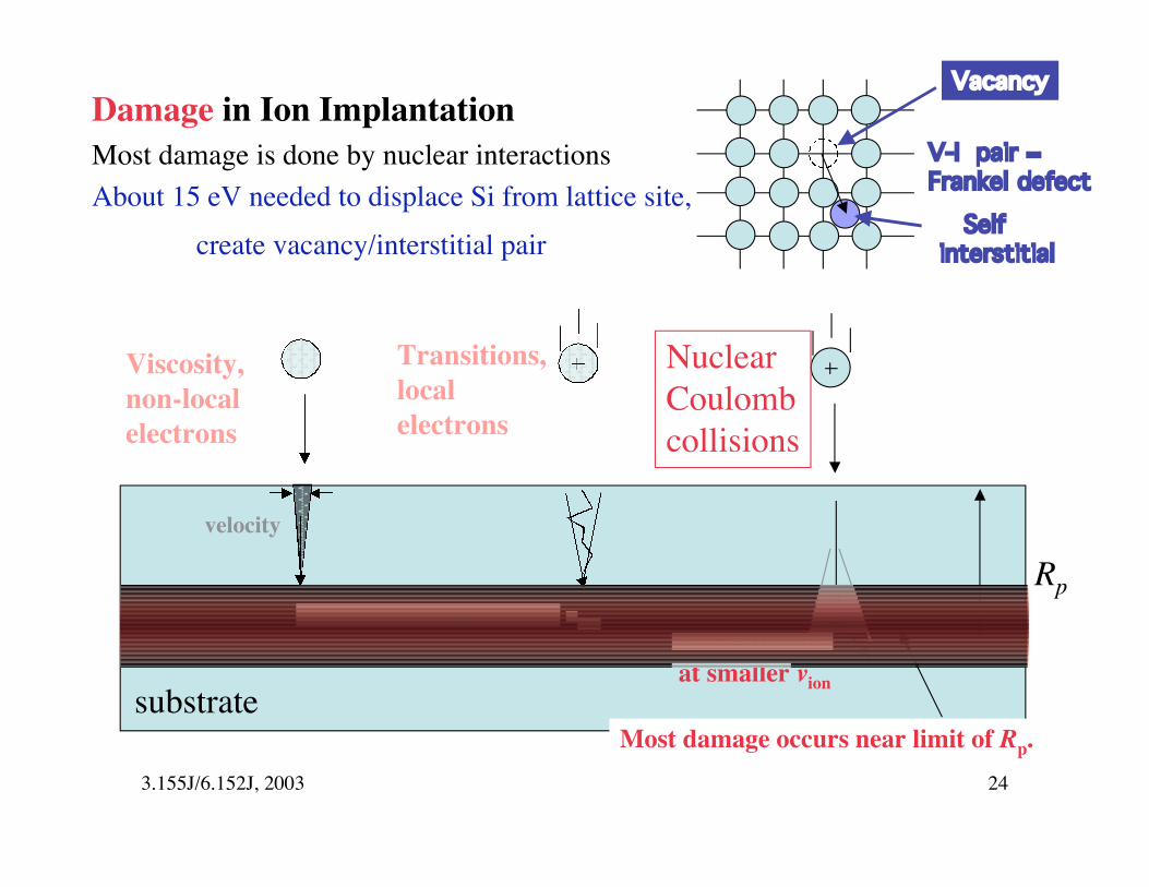
Damage in Ion Implantation VVaaccaannccyy
VV--II ppaaiirr ==Most damage is done by nuclear interactions
About 15 eV needed to displace Si from lattice site, FFrraannkkeell ddeeffeecctt
SSeellffcreate vacancy/interstitial pair iinntteerrssttiittiiaall
Transitions, NuclearViscosity, non-local local Coulomb electrons electrons collisions
R
substrate
velocity
More effective at smaller vion
More effective at larger vion
Rp.
ff iM ff i lff iM ff ti t lM ff i lM ff ti t lM ff ti t lM ff ti t lM ff ti t lMore effecti e at largerM ff ti t lMore effective at larger vMore effecti e at largerMore effective at larger vMore effective at larger vMore effective at larger vMore effective at larger vMore effective at larger vMore effective at larger vMore effective at larger vMore effective at larger vMore effective at larger vMore effective at larger vMore effective at larger vMore effective at larger vMore effective at larger viMore effective at larger vMore effective at larger viMore effective at larger viMore effective at larger viMore effective at larger viMore effective at larger vionMore effective at larger viMore effective at larger vionMore effective at larger viong iong iong iong iong iong iong iong iong iong ionionionionionff iM ff iff iM ff tiM ff iM ff tiM ff tiM ff tiM ff tiMore effecti eM ff tiMore effectiveMore effecti eMore effectiveMore effectiveMore effectiveMore effectiveMore effectiveMore effectiveMore effectiveMore effectiveMore effectiveMore effectiveMore effectiveMore effectiveMore effectiveMore effectiveMore effectiveMore effectiveMore effectiveMore effectiveMore effectiveMore effectiveMore effectiveMore effectivellt llllt llt llt llt ll
Most damage occurs near limit of
p
3.155J/6.152J, 2003 24
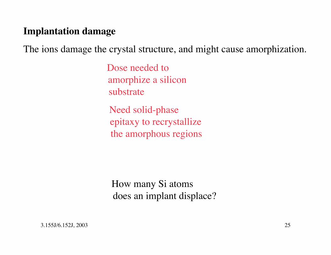
Implantation damage
The ions damage the crystal structure, and might cause amorphization.
Dose needed to amorphize a silicon substrate
Need solid-phase epitaxy to recrystallize the amorphous regions
How many Si atoms does an implant displace?
3.155J/6.152J, 2003 25
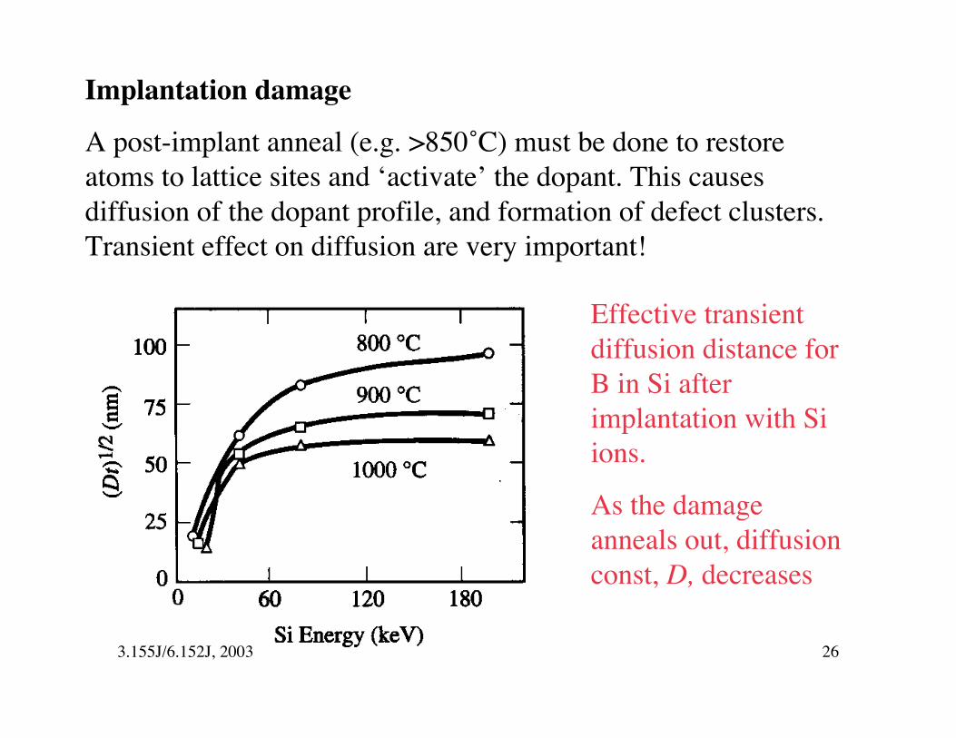
Implantation damage
A post-implant anneal (e.g. >850˚C) must be done to restore atoms to lattice sites and ‘activate’ the dopant. This causes diffusion of the dopant profile, and formation of defect clusters. Transient effect on diffusion are very important!
Effective transient diffusion distance for B in Si after implantation with Si ions.
As the damage anneals out, diffusion const, D, decreases
3.155J/6.152J, 2003 26
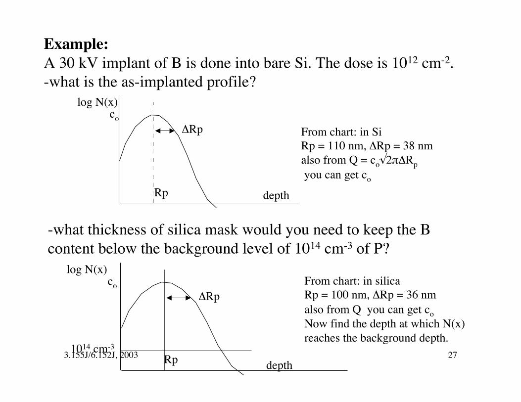
Example: A 30 kV implant of B is done into bare Si. The dose is 1012 cm-2. -what is the as-implanted profile?
log N(x) co
Rp
DRp From chart: in Si Rp = 110 nm, DRp = 38 nm also from Q = co√2pDRp
you can get co
depth
-what thickness of silica mask would you need to keep the B content below the background level of 1014 cm-3 of P?
log N(x) co From chart: in silica
DRp DRp = 36 nmRp = 100 nm, also from Q you can get c o Now find the depth at which N(x)
3.155J/6.152J, 20031014 cm-3
Rp depth 27
reaches the background depth.
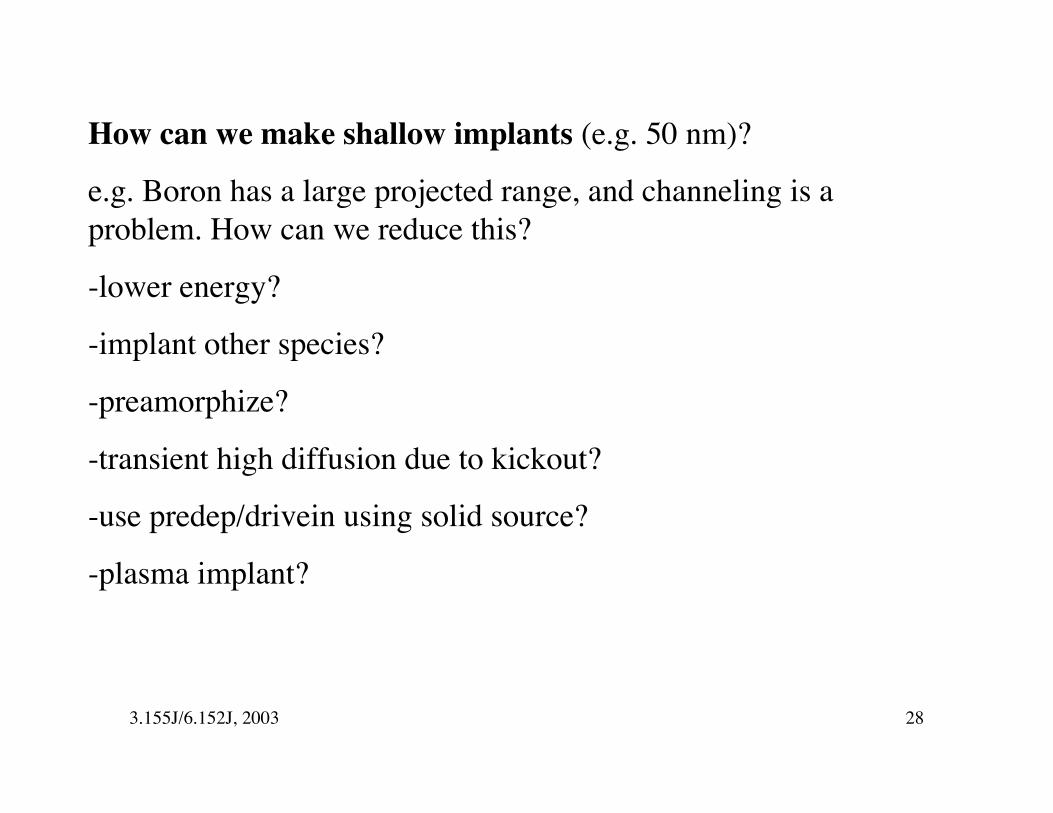
How can we make shallow implants (e.g. 50 nm)?
e.g. Boron has a large projected range, and channeling is aproblem. How can we reduce this?
-lower energy?
-implant other species?
-preamorphize?
-transient high diffusion due to kickout?
-use predep/drivein using solid source?
-plasma implant?
3.155J/6.152J, 2003 28
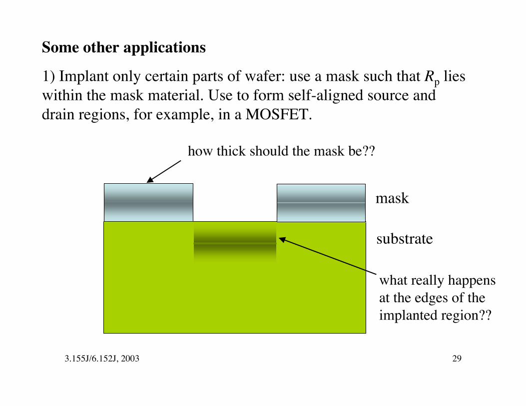
Some other applications
1) Implant only certain parts of wafer: use a mask such that Rp lies within the mask material. Use to form self-aligned source and drain regions, for example, in a MOSFET.
how thick should the mask be??
mask
substrate
what really happensat the edges of theimplanted region??
3.155J/6.152J, 2003 29
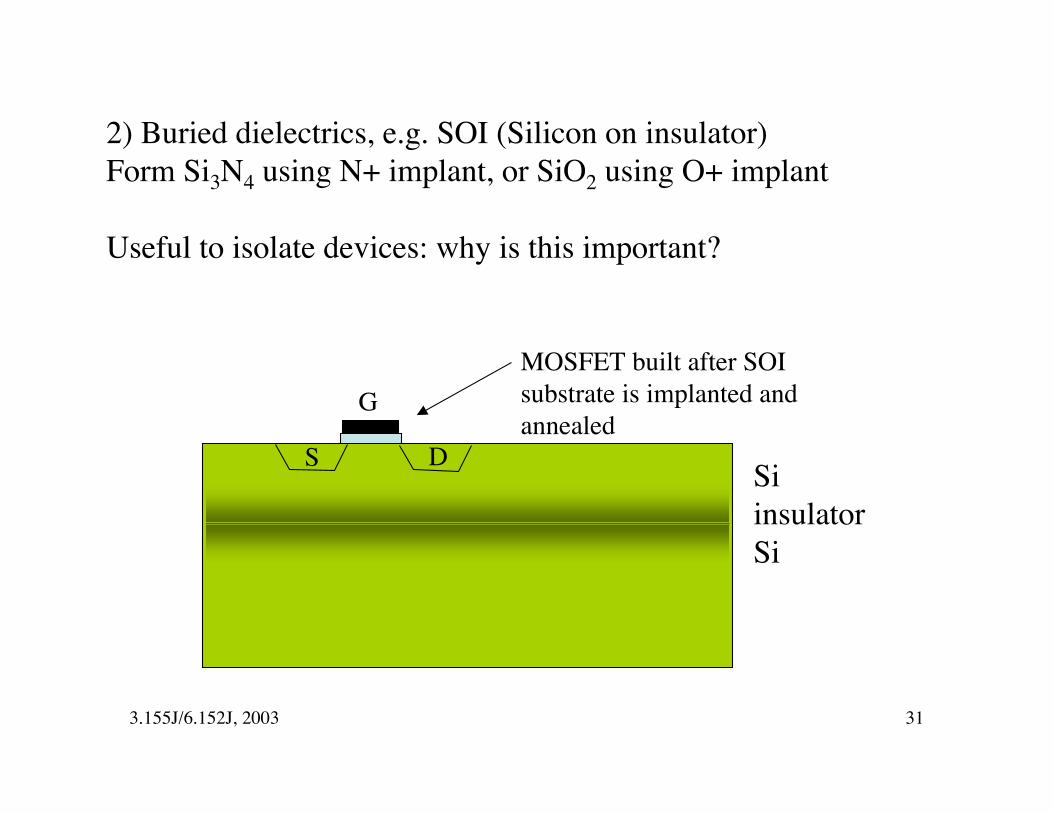
2) Buried dielectrics, e.g. SOI (Silicon on insulator) Form Si3N4 using N+ implant, or SiO2 using O+ implant
Useful to isolate devices: why is this important?
MOSFET built after SOI
G substrate is implanted and annealed
Si insulator Si
S D
3.155J/6.152J, 2003 31
Discussion
When do you prefer to use predep/drive in vs. ion implantation?
Can you think of cases where you could save some process stepsusing ion implantation?
What could the ion implant do to the background dopant?
Are there any particular problems in ion implantation for substratessuch as GaAs?
3.155J/6.152J, 2003 32