introduction: materials for electronics
TRANSCRIPT
Introduction: Materials for Electronics
It is widely recognized that the electronics and photonicsindustries are major parts of the world economy as well asbeing responsible for many of the advanced technologies thathave added so much to our lives. However, it is not generallyknown that many of the products they have provided arenot simply the province of physics and electrical engineering,as commonly perceived, but are built on complex chemistryand chemical engineering platforms. In fact, this is a majorarena where nanotechnology is practiced. This issue ofChemical Reviews covers a number of diverse contributionsto Electronic Materials that are based on chemical andmaterials sciences.
Let us begin with semiconductor technology. The ever-shrinking dimensions of devices have required better per-formance of patterning materials, and some of the changesare discussed in two articles by Sanders and Kim, Park, andHinsberg on modern lithography and self-assembly. Thinfilms of both active and passive materials are criticalcomponents and have often been deposited by chemicalvapor deposition (CVD) processes. However, thinner filmsrequire greater control, and atomic layer deposition, reviewedby George, has assumed more importance. New, ultrathin,uniform dielectric layers, with k values as high as possible,and their applications are reviewed by Ponce Ortiz, Facchetti,and Marks, while advances in back-end-of-the-line (BEOL)insulator materials are covered by Volksen, Miller, andDubois. A desire to implement new nanostructures has ledto many new areas of work. The preparation, properties, andapplications of colloidal nanocrystals are reviewed by
Talapin, Lee, Kovalenko, and Shevchenko, and siliconnanowire science is summarized by Schmidt, Witteman, andGosele. Semiconductor nanowire applications for energyconversion are discussed by Hochbaum and Yang.
Many of the wet chemical processes cannot be pushed tothe nanoscopic dimensions needed because solvent viscosity/surface tension damages features and supercritical fluids(SCFs) provide an advantage. Romang and Watkins covercurrent issues in this area. Finally, the critical need for planarsurfaces in CMOS integration has been answered bychemical-mechanical planarization (CMP) of metals anddielectric surfaces, a mixture of abrasion and chemicaltransformation, and Krishnan, Nalaskowski, and Cook bringus up to date on progress here.
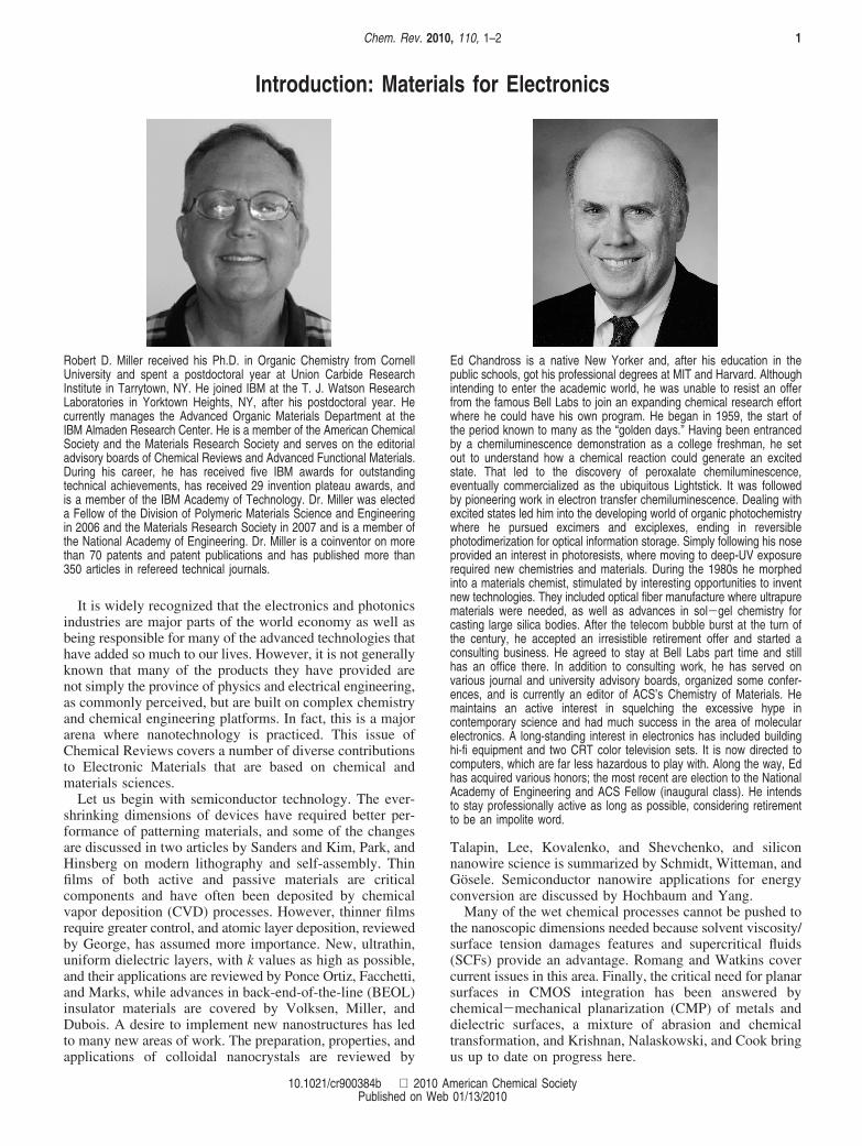
Robert D. Miller received his Ph.D. in Organic Chemistry from CornellUniversity and spent a postdoctoral year at Union Carbide ResearchInstitute in Tarrytown, NY. He joined IBM at the T. J. Watson ResearchLaboratories in Yorktown Heights, NY, after his postdoctoral year. Hecurrently manages the Advanced Organic Materials Department at theIBM Almaden Research Center. He is a member of the American ChemicalSociety and the Materials Research Society and serves on the editorialadvisory boards of Chemical Reviews and Advanced Functional Materials.During his career, he has received five IBM awards for outstandingtechnical achievements, has received 29 invention plateau awards, andis a member of the IBM Academy of Technology. Dr. Miller was electeda Fellow of the Division of Polymeric Materials Science and Engineeringin 2006 and the Materials Research Society in 2007 and is a member ofthe National Academy of Engineering. Dr. Miller is a coinventor on morethan 70 patents and patent publications and has published more than350 articles in refereed technical journals.
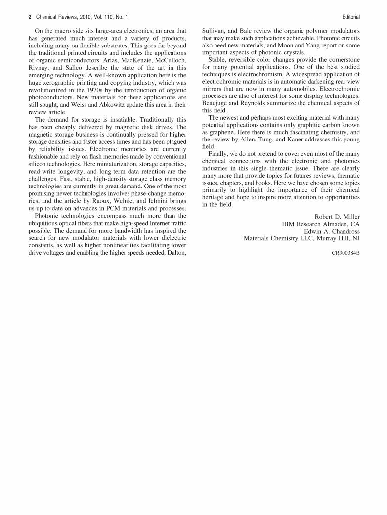
Ed Chandross is a native New Yorker and, after his education in thepublic schools, got his professional degrees at MIT and Harvard. Althoughintending to enter the academic world, he was unable to resist an offerfrom the famous Bell Labs to join an expanding chemical research effortwhere he could have his own program. He began in 1959, the start ofthe period known to many as the “golden days.” Having been entrancedby a chemiluminescence demonstration as a college freshman, he setout to understand how a chemical reaction could generate an excitedstate. That led to the discovery of peroxalate chemiluminescence,eventually commercialized as the ubiquitous Lightstick. It was followedby pioneering work in electron transfer chemiluminescence. Dealing withexcited states led him into the developing world of organic photochemistrywhere he pursued excimers and exciplexes, ending in reversiblephotodimerization for optical information storage. Simply following his noseprovided an interest in photoresists, where moving to deep-UV exposurerequired new chemistries and materials. During the 1980s he morphedinto a materials chemist, stimulated by interesting opportunities to inventnew technologies. They included optical fiber manufacture where ultrapurematerials were needed, as well as advances in sol-gel chemistry forcasting large silica bodies. After the telecom bubble burst at the turn ofthe century, he accepted an irresistible retirement offer and started aconsulting business. He agreed to stay at Bell Labs part time and stillhas an office there. In addition to consulting work, he has served onvarious journal and university advisory boards, organized some confer-ences, and is currently an editor of ACS’s Chemistry of Materials. Hemaintains an active interest in squelching the excessive hype incontemporary science and had much success in the area of molecularelectronics. A long-standing interest in electronics has included buildinghi-fi equipment and two CRT color television sets. It is now directed tocomputers, which are far less hazardous to play with. Along the way, Edhas acquired various honors; the most recent are election to the NationalAcademy of Engineering and ACS Fellow (inaugural class). He intendsto stay professionally active as long as possible, considering retirementto be an impolite word.
Chem. Rev. 2010, 110, 1–2 1
10.1021/cr900384b 2010 American Chemical SocietyPublished on Web 01/13/2010
On the macro side sits large-area electronics, an area thathas generated much interest and a variety of products,including many on flexible substrates. This goes far beyondthe traditional printed circuits and includes the applicationsof organic semiconductors. Arias, MacKenzie, McCulloch,Rivnay, and Salleo describe the state of the art in thisemerging technology. A well-known application here is thehuge xerographic printing and copying industry, which wasrevolutionized in the 1970s by the introduction of organicphotoconductors. New materials for these applications arestill sought, and Weiss and Abkowitz update this area in theirreview article.
The demand for storage is insatiable. Traditionally thishas been cheaply delivered by magnetic disk drives. Themagnetic storage business is continually pressed for higherstorage densities and faster access times and has been plaguedby reliability issues. Electronic memories are currentlyfashionable and rely on flash memories made by conventionalsilicon technologies. Here miniaturization, storage capacities,read-write longevity, and long-term data retention are thechallenges. Fast, stable, high-density storage class memorytechnologies are currently in great demand. One of the mostpromising newer technologies involves phase-change memo-ries, and the article by Raoux, Welnic, and Ielmini bringsus up to date on advances in PCM materials and processes.
Photonic technologies encompass much more than theubiquitious optical fibers that make high-speed Internet trafficpossible. The demand for more bandwidth has inspired thesearch for new modulator materials with lower dielectricconstants, as well as higher nonlinearities facilitating lowerdrive voltages and enabling the higher speeds needed. Dalton,
Sullivan, and Bale review the organic polymer modulatorsthat may make such applications achievable. Photonic circuitsalso need new materials, and Moon and Yang report on someimportant aspects of photonic crystals.
Stable, reversible color changes provide the cornerstonefor many potential applications. One of the best studiedtechniques is electrochromism. A widespread application ofelectrochromic materials is in automatic darkening rear viewmirrors that are now in many automobiles. Electrochromicprocesses are also of interest for some display technologies.Beaujuge and Reynolds summarize the chemical aspects ofthis field.
The newest and perhaps most exciting material with manypotential applications contains only graphitic carbon knownas graphene. Here there is much fascinating chemistry, andthe review by Allen, Tung, and Kaner addresses this youngfield.
Finally, we do not pretend to cover even most of the manychemical connections with the electronic and photonicsindustries in this single thematic issue. There are clearlymany more that provide topics for futures reviews, thematicissues, chapters, and books. Here we have chosen some topicsprimarily to highlight the importance of their chemicalheritage and hope to inspire more attention to opportunitiesin the field.
Robert D. MillerIBM Research Almaden, CA
Edwin A. ChandrossMaterials Chemistry LLC, Murray Hill, NJ
CR900384B
2 Chemical Reviews, 2010, Vol. 110, No. 1 Editorial