intel fpga monitor program tutorial - yonsei...
TRANSCRIPT
Intel FPGA Monitor ProgramTutorial for ARM
For Quartus Prime 16.1
1 Introduction
This tutorial presents an introduction to the Intel FPGA Monitor Program that can be used to compile, assemble,download and debug programs for ARM® Cortex-A9 processor, which is a processor implemented as a hardwareblock in Intel’s Cyclone® V SoC FPGA devices. The tutorial is intended for a user who wishes to use an ARM-basedsystem on an Intel Development and Education board. It gives step-by-step instructions that illustrate the featuresof the Monitor Program. In addition to supporting the ARM-based programs, the Monitor Program can also be usedwith the Nios II-based programs. For this application, consult the tutorial Intel FPGA Monitor Program for Nios II.
The Monitor Program is a software application which runs on a host PC, and communicates with an ARM-basedhardware system on an FPGA board. It can be used to compile/assemble an ARM software application, downloadthe application onto the FPGA board, and then debug the running application. It provides features that allow theuser to:
• Set up an ARM project that specifies a desired hardware system and software program
• Download the hardware system onto an FPGA board
• Compile software programs, specified in assembly language or C, and download the resulting machine codeinto the hardware system
• Display the machine code stored in memory
• Run the ARM processor, either continuously or by single-stepping instructions
• Examine and modify the contents of processor registers
• Examine and modify the contents of memory, as well as memory-mapped registers in I/O devices
• Set breakpoints that stop the execution of a program at a specified address, or when certain conditions are met
The process of downloading and debugging an ARM program requires an FPGA board that contains the ARMhard processor system (HPS) hardware. In this tutorial it is assumed that the reader has access to the DE1-SoCDevelopment and Education board, connected to a computer that has Quartus Prime and Nios II Embedded DesignSuite (EDS) software installed. Although a reader who does not have access to an FPGA board will not be able toexecute the Monitor Program commands described in the tutorial, it should still be possible to follow the discussion.
Intel Corporation - FPGA University ProgramNovember 2016
1

INTEL FPGA MONITOR PROGRAM TUTORIAL FOR ARM For Quartus Prime 16.1
1.1 Who should use the Monitor Program
The Monitor Program is intended to be used in an educational environment by professors and students. It is notintended for commercial use.
2 Installing the Monitor Program
The Monitor Program is released as part of the University Program Design Suite (UPDS). Before the UPDS can beinstalled on a computer, it is necessary to first install the Quartus Prime CAD software (either the Lite, Standard orPro Edition) and the Nios II Embedded Design Suite (EDS). A particular release of the Monitor Program can be usedonly with a corresponding version of the Quartus Prime software and Nios II EDS. This software can be obtainedfrom the Download Center on Intel’s website at university.altera.com. To locate the software select DOWNLOADSand then download the desired version.
Once the Quartus Prime software and Nios II EDS are installed, the UPDS can be installed.
Note that if the Quartus Prime software is re-installed at some future time, then it will be necessary to re-install theMonitor Program at that time.
2.1 Using a Windows Operating System
When using a Windows operating system, perform the following:
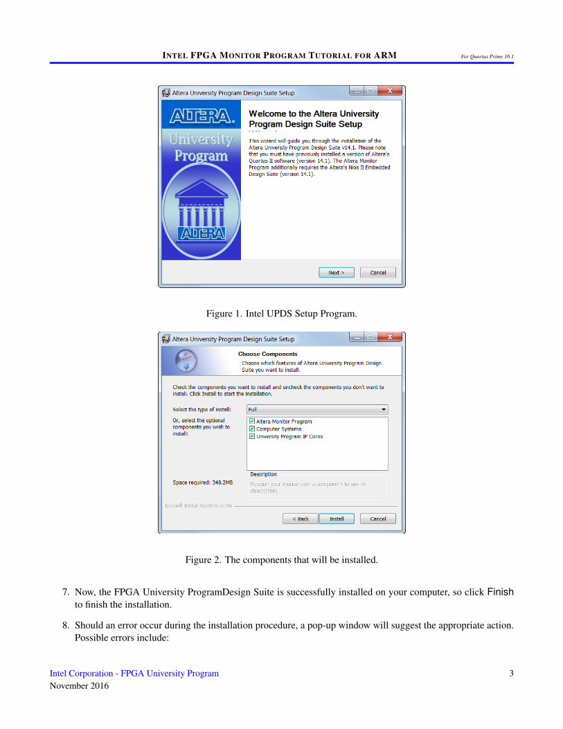
1. Install the UPDS from the University Program section of Intel’s website. It can be found by going touniversity.altera.com and choosing SUPPORT followed by Training and University Program. Then,select software tools > Intel FPGA Monitor Program. Specify the installed version of Quartus Prime soft-ware. Then click on the EXE item in the displayed table, which links to an installation program called al-tera_upds_setup.exe. When prompted to Run or Save this file, select Run.
2. The first screen of the installer is shown in Figure 1. Click on the Next button.
3. The installer will display the License Agreement; if you accept the terms of this agreement, then click I Agreeto continue.
4. The installer now displays the root directory where the FPGA University Program Design Suite will be in-stalled. Click Next.
5. The next screen, shown in Figure 2, lists the components that will be installed, which include the MonitorProgram software and University Program IP Cores. These IP Cores provide a number of I/O device circuitsthat can be used in hardware systems to be implemented on the FPGA board.
6. The installer is now ready to begin copying files. Click Install to proceed and then click Next after the instal-lation has been completed. If you answered Yes when prompted about placing a shortcut on your Windows
Desktop, then an icon is provided on the Desktop that can be used to start the Monitor Program.
2 Intel Corporation - FPGA University ProgramNovember 2016
INTEL FPGA MONITOR PROGRAM TUTORIAL FOR ARM For Quartus Prime 16.1
Figure 1. Intel UPDS Setup Program.
Figure 2. The components that will be installed.
7. Now, the FPGA University ProgramDesign Suite is successfully installed on your computer, so click Finishto finish the installation.
8. Should an error occur during the installation procedure, a pop-up window will suggest the appropriate action.Possible errors include:
Intel Corporation - FPGA University ProgramNovember 2016
3

INTEL FPGA MONITOR PROGRAM TUTORIAL FOR ARM For Quartus Prime 16.1
• Quartus Prime software is not installed or the Quartus Prime version is incorrect.
• Nios II EDS software is not installed or the version is incorrect.
2.2 Using a Linux Operating System
When using a Linux operating system, perform the following:
1. Install the UPDS from the University Program section of Intel’s website. It can be found by going touniversity.altera.com and choosing SUPPORT followed by Training and University Program. Then,select software tools > Intel FPGA Monitor Program. Specify the installed version of Quartus Prime soft-ware. Then click on the TAR item in the displayed table, which links to an installation tarball called al-tera_upds_setup.tar. Save this file to a directory of your choosing.
2. Using a console, navigate to the directory to which the file was saved. Extract the contents of altera_upds_setup.tarusing the following command: tar -xf altera_upds_setup.tar.
3. Among the extracted files is a shell script named install_altera_upds which will be used to install the UPDS.Ensure that the script is executable by using the following command: chmod +x install_altera_upds.
4. Run the installation script with superuser privileges by using the following command: sudo ./install_altera_upds.
5. Follow the instructions displayed by the script to complete the installation.
3 Main Features of the Monitor Program
Each ARM software application that is developed with the Monitor Program is called a project. The MonitorProgram works on one project at a time and keeps all information for that project in a single directory in the filesystem. The first step is to create a directory to hold the project’s files. To store the design files for this tutorial, wewill use a directory named Monitor_Tutorial. The running example for this tutorial is a simple assembly-languageprogram that controls some lights on a DE1-SoC board.
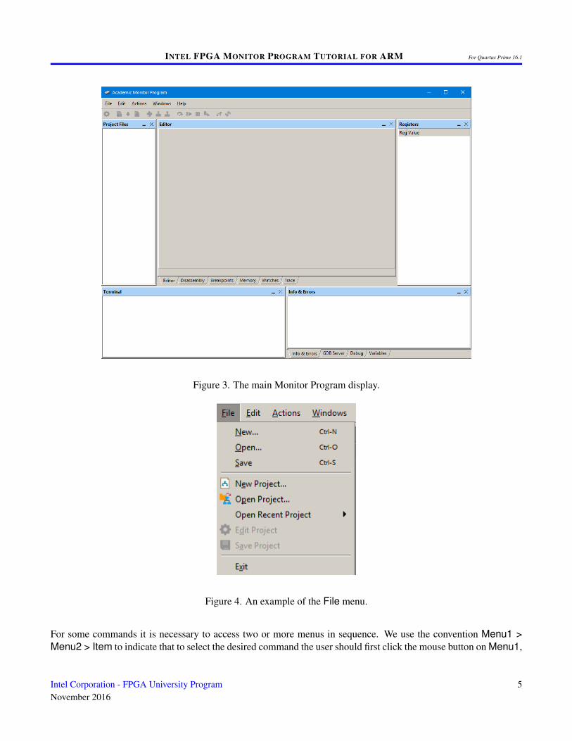
If you are using a Windows operating system, then start the Monitor Program software either by double-clicking itsicon on the Windows Desktop or by accessing the program in the Windows Start menu under Intel > UniversityProgram > Intel FPGA Monitor Program. You should see a display similar to the one in Figure 3.
If you are using a Linux operating system, then start the Monitor Program software by running the altera-monitor-program shell script located in <path to Intel software>/University Program/Monitor Program/bin. You should seea display similar to the one in Figure 3.
This display consists of several windows that provide access to all of the features of the Monitor Program, which theuser selects with the computer mouse. Most of the commands provided by the Monitor Program can be accessed byusing a set of menus that are located below the title bar. For example, in Figure 3 clicking the left mouse button onthe File command opens the menu shown in Figure 4. Clicking the left mouse button on the entry Exit exits fromthe Monitor Program. In most cases, whenever the mouse is used to select something, the left button is used. Hencewe will not normally specify which button to press.
4 Intel Corporation - FPGA University ProgramNovember 2016
INTEL FPGA MONITOR PROGRAM TUTORIAL FOR ARM For Quartus Prime 16.1
Figure 3. The main Monitor Program display.
Figure 4. An example of the File menu.
For some commands it is necessary to access two or more menus in sequence. We use the convention Menu1 >Menu2 > Item to indicate that to select the desired command the user should first click the mouse button on Menu1,
Intel Corporation - FPGA University ProgramNovember 2016
5

INTEL FPGA MONITOR PROGRAM TUTORIAL FOR ARM For Quartus Prime 16.1
then within this menu click on Menu2, and then within Menu2 click on Item. For example, File > Exit uses themouse to exit from the Monitor Program. Many commands can alternatively be invoked by clicking on an icondisplayed in the Monitor Program window. To see the command associated with an icon, position the mouse overthe icon and a tooltip will appear that displays the command name.
It is possible to modify the organization of the Monitor Program display in Figure 3 in many ways. Section 8 showshow to move, resize, close, and open windows within the Monitor Program display.
3.1 Creating a Project
To start working on an ARM software application we first have to create a new project, as follows:
1. Select File > New Project to open the New Project Wizard, which leads to the screen in Figure 5. The Wizardpresents a sequence of screens for defining a new project. Each screen includes a number of dialogs, as wellas a message area at the bottom of the window. The message area is used to display error and informationmessages associated with the dialogs in the window. Double-clicking the mouse on an error message movesthe cursor into the dialog box that contains the source of the error.
Figure 5. Specifying the project directory and name.
In Figure 5 we have specified the file system directory D:\Monitor_Tutorial and the project name Moni-tor_Tutorial. For simplicity, we have used a project name that matches the directory name, but this is not
6 Intel Corporation - FPGA University ProgramNovember 2016

INTEL FPGA MONITOR PROGRAM TUTORIAL FOR ARM For Quartus Prime 16.1
required.
If the file system directory specified for the project does not already exist, a message will be displayed indicat-ing that this new directory will be created. To select an existing directory by browsing through the file system,click on the Browse button. Note that a given directory may contain at most one project.
The Monitor Program can be used with either an ARM-based system or a Nios II-based system. The choiceof a processor is made in the window in Figure 5 in the box labeled Architecture. We have chosen the ARMCortex-A9 architecture for this tutorial.
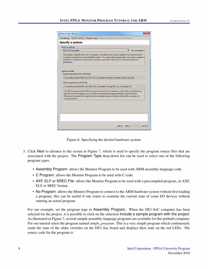
2. Click Next to advance to the window shown in Figure 6, which is used to specify a particular system. Ahardware system to be implemented on the FPGA board is usually generated by using Quartus’s Qsys tool.Information about creating systems using Qsys can be found in the Introduction to the Intel Qsys SystemIntegration Tool tutorial, which is available in the University Program section of Intel’s website.
A system designed and generated by using Quartus Prime and its Qsys tool is described in SOPCInfo andSOF files. The former gives a high-level description of the system. The latter represents the FPGA circuit thatimplements the designed system; this file can be downloaded into the FPGA chip on the board that is beingused.
The drop-down list on the Select a system pane can be used to choose the system to be used in the project.There are three possibilities: a prebuilt DE1-SoC Computer system, a custom system created by the user,and a generic ARM Cortex-A9 System.
The Monitor Program includes a prebuilt computer system for the DE1-SoC boards, called the DE1-SoCComputer, which includes a number of interfaces to input/output devices implemented in the FPGA fabric ofthe chip. This computer was created using Quartus Prime and its Qsys tool. It is represented by .sopcinfo and.sof files which are automatically included when this computer is selected.
If a custom system is selected, then the user must manually specify the .sopcinfo and .sof files that define therequired system in the System details pane.
The third option is to use the generic ARM Cortex-A9 system. In this case no design files are used, and onlythe resources that are directly associated with the HPS part of the FPGA device are available. For example,application programs that do not involve resources implemented in the FPGA fabric can be run using thissystem.
For this tutorial we have chosen DE1-SoC Computer, as depicted in Figure 6. In the top right corner ofthe screen there is a Documentation button. Clicking on this button opens a user guide that provides allinformation needed for developing ARM programs for the DE1-SoC Computer, such as the memory map foraddressing all of the I/O devices in the system. This file can also be accessed at a later time by using thecommand Settings > System Settings and then clicking on the Documentation button.
Intel Corporation - FPGA University ProgramNovember 2016
7
INTEL FPGA MONITOR PROGRAM TUTORIAL FOR ARM For Quartus Prime 16.1
Figure 6. Specifying the desired hardware system.
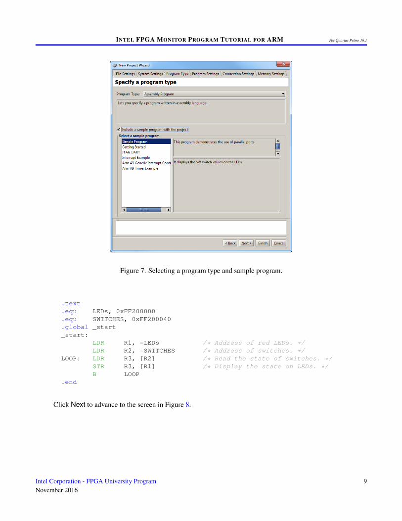
3. Click Next to advance to the screen in Figure 7, which is used to specify the program source files that areassociated with the project. The Program Type drop-down list can be used to select one of the followingprogram types:
• Assembly Program: allows the Monitor Program to be used with ARM assembly-language code.
• C Program: allows the Monitor Program to be used with C code.
• AXF, ELF or SREC File: allows the Monitor Program to be used with a precompiled program, in AXF,ELF or SREC format.
• No Program: allows the Monitor Program to connect to the ARM hardware system without first loadinga program; this can be useful if one wants to examine the current state of some I/O devices withoutrunning an actual program.
For our example, set the program type to Assembly Program. When the DE1-SoC computer has beenselected for the project, it is possible to click on the selection Include a sample program with the project.As illustrated in Figure 7, several sample assembly-language programs are available for this prebuilt computer.For our tutorial select the program named simple_program. This is a very simple program which continuouslyreads the state of the slider switches on the DE1-Soc board and displays their state on the red LEDs. Thesource code for the program is:
8 Intel Corporation - FPGA University ProgramNovember 2016
INTEL FPGA MONITOR PROGRAM TUTORIAL FOR ARM For Quartus Prime 16.1
Figure 7. Selecting a program type and sample program.
.text
.equ LEDs, 0xFF200000
.equ SWITCHES, 0xFF200040
.global _start_start:
LDR R1, =LEDs /* Address of red LEDs. */LDR R2, =SWITCHES /* Address of switches. */
LOOP: LDR R3, [R2] /* Read the state of switches. */STR R3, [R1] /* Display the state on LEDs. */B LOOP
.end
Click Next to advance to the screen in Figure 8.
Intel Corporation - FPGA University ProgramNovember 2016
9
INTEL FPGA MONITOR PROGRAM TUTORIAL FOR ARM For Quartus Prime 16.1
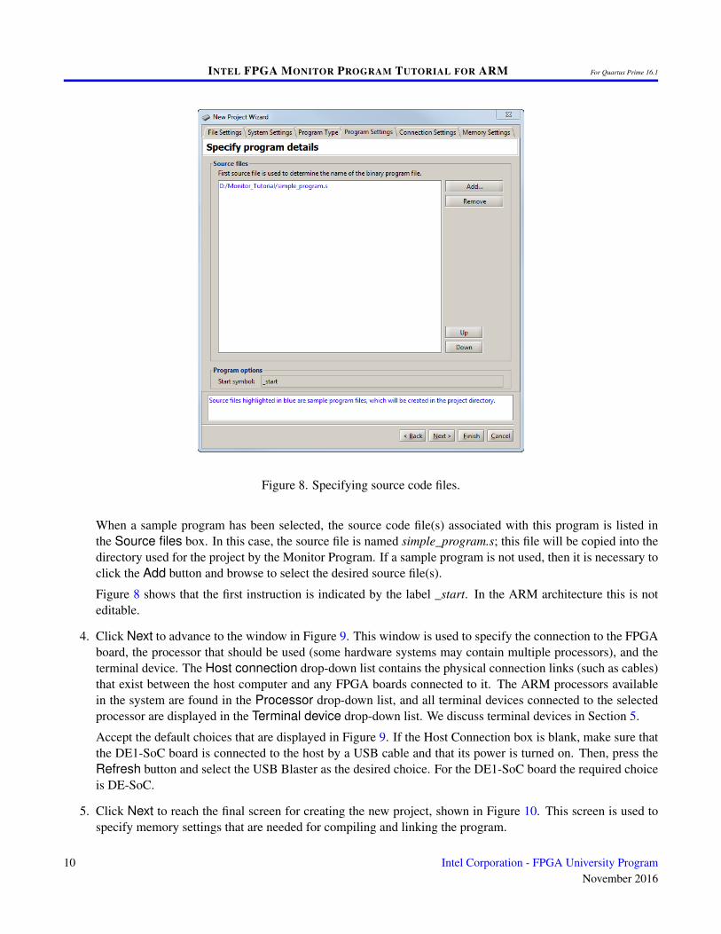
Figure 8. Specifying source code files.
When a sample program has been selected, the source code file(s) associated with this program is listed inthe Source files box. In this case, the source file is named simple_program.s; this file will be copied into thedirectory used for the project by the Monitor Program. If a sample program is not used, then it is necessary toclick the Add button and browse to select the desired source file(s).
Figure 8 shows that the first instruction is indicated by the label _start. In the ARM architecture this is noteditable.
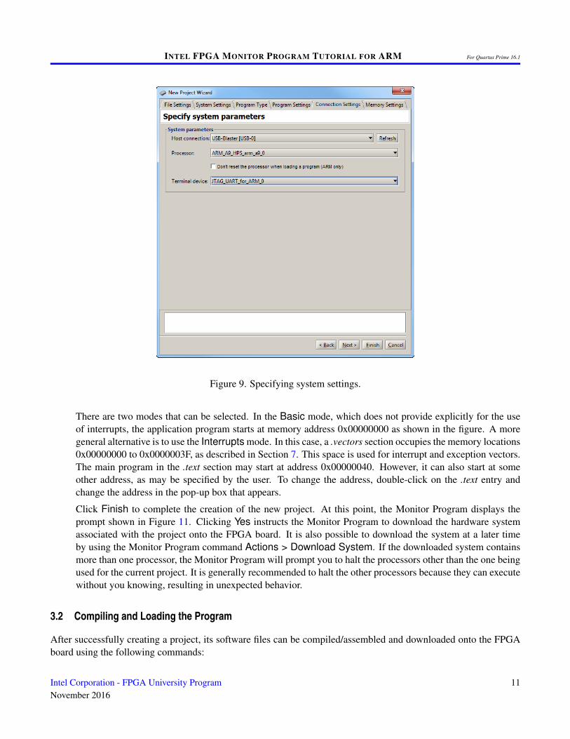
4. Click Next to advance to the window in Figure 9. This window is used to specify the connection to the FPGAboard, the processor that should be used (some hardware systems may contain multiple processors), and theterminal device. The Host connection drop-down list contains the physical connection links (such as cables)that exist between the host computer and any FPGA boards connected to it. The ARM processors availablein the system are found in the Processor drop-down list, and all terminal devices connected to the selectedprocessor are displayed in the Terminal device drop-down list. We discuss terminal devices in Section 5.
Accept the default choices that are displayed in Figure 9. If the Host Connection box is blank, make sure thatthe DE1-SoC board is connected to the host by a USB cable and that its power is turned on. Then, press theRefresh button and select the USB Blaster as the desired choice. For the DE1-SoC board the required choiceis DE-SoC.
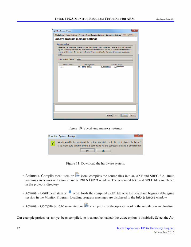
5. Click Next to reach the final screen for creating the new project, shown in Figure 10. This screen is used tospecify memory settings that are needed for compiling and linking the program.
10 Intel Corporation - FPGA University ProgramNovember 2016
INTEL FPGA MONITOR PROGRAM TUTORIAL FOR ARM For Quartus Prime 16.1
Figure 9. Specifying system settings.
There are two modes that can be selected. In the Basic mode, which does not provide explicitly for the useof interrupts, the application program starts at memory address 0x00000000 as shown in the figure. A moregeneral alternative is to use the Interrupts mode. In this case, a .vectors section occupies the memory locations0x00000000 to 0x0000003F, as described in Section 7. This space is used for interrupt and exception vectors.The main program in the .text section may start at address 0x00000040. However, it can also start at someother address, as may be specified by the user. To change the address, double-click on the .text entry andchange the address in the pop-up box that appears.
Click Finish to complete the creation of the new project. At this point, the Monitor Program displays theprompt shown in Figure 11. Clicking Yes instructs the Monitor Program to download the hardware systemassociated with the project onto the FPGA board. It is also possible to download the system at a later timeby using the Monitor Program command Actions > Download System. If the downloaded system containsmore than one processor, the Monitor Program will prompt you to halt the processors other than the one beingused for the current project. It is generally recommended to halt the other processors because they can executewithout you knowing, resulting in unexpected behavior.
3.2 Compiling and Loading the Program
After successfully creating a project, its software files can be compiled/assembled and downloaded onto the FPGAboard using the following commands:
Intel Corporation - FPGA University ProgramNovember 2016
11
INTEL FPGA MONITOR PROGRAM TUTORIAL FOR ARM For Quartus Prime 16.1
Figure 10. Specifying memory settings.
Figure 11. Download the hardware system.
• Actions > Compile menu item or icon: compiles the source files into an AXF and SREC file. Buildwarnings and errors will show up in the Info & Errors window. The generated AXF and SREC files are placedin the project’s directory.
• Actions > Load menu item or icon: loads the compiled SREC file onto the board and begins a debuggingsession in the Monitor Program. Loading progress messages are displayed in the Info & Errors window.
• Actions > Compile & Load menu item or icon: performs the operations of both compilation and loading.
Our example project has not yet been compiled, so it cannot be loaded (the Load option is disabled). Select the Ac-
12 Intel Corporation - FPGA University ProgramNovember 2016
INTEL FPGA MONITOR PROGRAM TUTORIAL FOR ARM For Quartus Prime 16.1
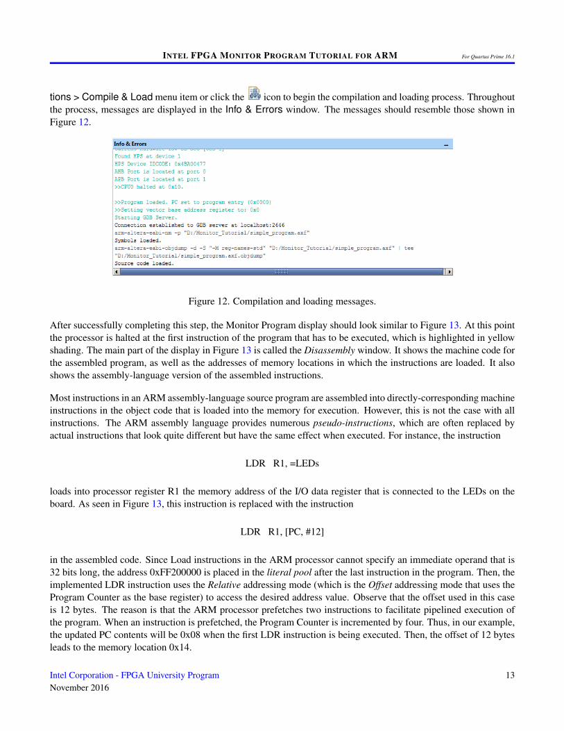
tions > Compile & Load menu item or click the icon to begin the compilation and loading process. Throughoutthe process, messages are displayed in the Info & Errors window. The messages should resemble those shown inFigure 12.
Figure 12. Compilation and loading messages.
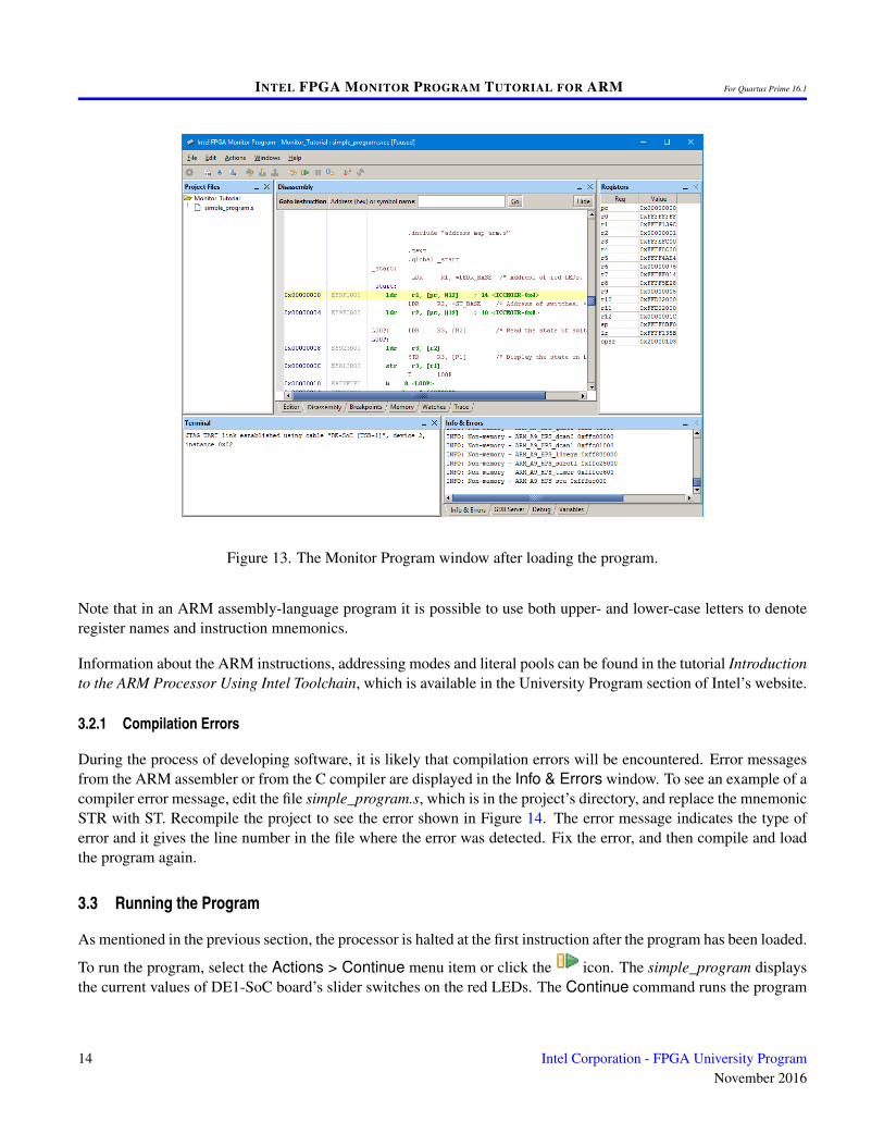
After successfully completing this step, the Monitor Program display should look similar to Figure 13. At this pointthe processor is halted at the first instruction of the program that has to be executed, which is highlighted in yellowshading. The main part of the display in Figure 13 is called the Disassembly window. It shows the machine code forthe assembled program, as well as the addresses of memory locations in which the instructions are loaded. It alsoshows the assembly-language version of the assembled instructions.
Most instructions in an ARM assembly-language source program are assembled into directly-corresponding machineinstructions in the object code that is loaded into the memory for execution. However, this is not the case with allinstructions. The ARM assembly language provides numerous pseudo-instructions, which are often replaced byactual instructions that look quite different but have the same effect when executed. For instance, the instruction
LDR R1, =LEDs
loads into processor register R1 the memory address of the I/O data register that is connected to the LEDs on theboard. As seen in Figure 13, this instruction is replaced with the instruction
LDR R1, [PC, #12]
in the assembled code. Since Load instructions in the ARM processor cannot specify an immediate operand that is32 bits long, the address 0xFF200000 is placed in the literal pool after the last instruction in the program. Then, theimplemented LDR instruction uses the Relative addressing mode (which is the Offset addressing mode that uses theProgram Counter as the base register) to access the desired address value. Observe that the offset used in this caseis 12 bytes. The reason is that the ARM processor prefetches two instructions to facilitate pipelined execution ofthe program. When an instruction is prefetched, the Program Counter is incremented by four. Thus, in our example,the updated PC contents will be 0x08 when the first LDR instruction is being executed. Then, the offset of 12 bytesleads to the memory location 0x14.
Intel Corporation - FPGA University ProgramNovember 2016
13
INTEL FPGA MONITOR PROGRAM TUTORIAL FOR ARM For Quartus Prime 16.1
Figure 13. The Monitor Program window after loading the program.
Note that in an ARM assembly-language program it is possible to use both upper- and lower-case letters to denoteregister names and instruction mnemonics.
Information about the ARM instructions, addressing modes and literal pools can be found in the tutorial Introductionto the ARM Processor Using Intel Toolchain, which is available in the University Program section of Intel’s website.
3.2.1 Compilation Errors
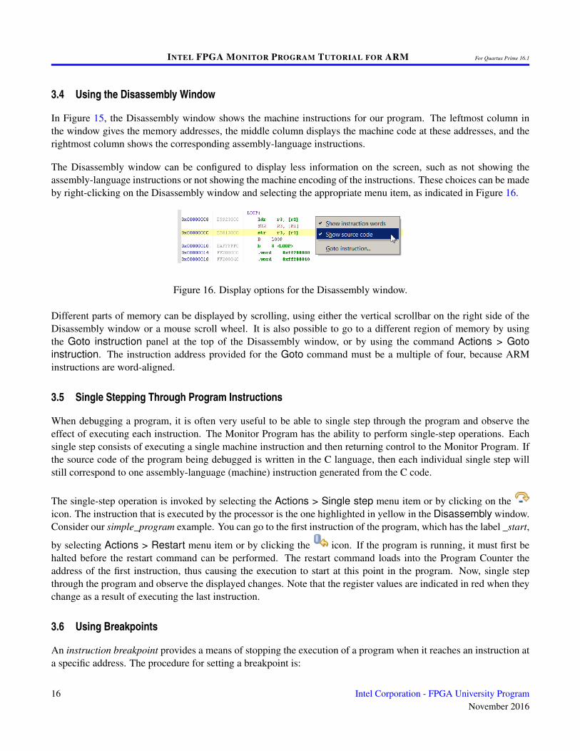
During the process of developing software, it is likely that compilation errors will be encountered. Error messagesfrom the ARM assembler or from the C compiler are displayed in the Info & Errors window. To see an example of acompiler error message, edit the file simple_program.s, which is in the project’s directory, and replace the mnemonicSTR with ST. Recompile the project to see the error shown in Figure 14. The error message indicates the type oferror and it gives the line number in the file where the error was detected. Fix the error, and then compile and loadthe program again.
3.3 Running the Program
As mentioned in the previous section, the processor is halted at the first instruction after the program has been loaded.
To run the program, select the Actions > Continue menu item or click the icon. The simple_program displaysthe current values of DE1-SoC board’s slider switches on the red LEDs. The Continue command runs the program
14 Intel Corporation - FPGA University ProgramNovember 2016
INTEL FPGA MONITOR PROGRAM TUTORIAL FOR ARM For Quartus Prime 16.1
Figure 14. An example of a compiler error message.
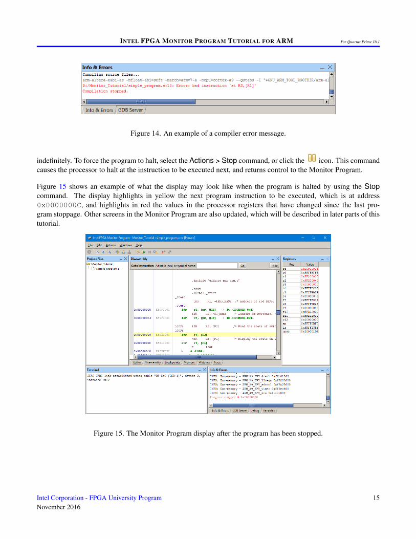
indefinitely. To force the program to halt, select the Actions > Stop command, or click the icon. This commandcauses the processor to halt at the instruction to be executed next, and returns control to the Monitor Program.
Figure 15 shows an example of what the display may look like when the program is halted by using the Stopcommand. The display highlights in yellow the next program instruction to be executed, which is at address0x0000000C, and highlights in red the values in the processor registers that have changed since the last pro-gram stoppage. Other screens in the Monitor Program are also updated, which will be described in later parts of thistutorial.
Figure 15. The Monitor Program display after the program has been stopped.
Intel Corporation - FPGA University ProgramNovember 2016
15
INTEL FPGA MONITOR PROGRAM TUTORIAL FOR ARM For Quartus Prime 16.1
3.4 Using the Disassembly Window
In Figure 15, the Disassembly window shows the machine instructions for our program. The leftmost column inthe window gives the memory addresses, the middle column displays the machine code at these addresses, and therightmost column shows the corresponding assembly-language instructions.
The Disassembly window can be configured to display less information on the screen, such as not showing theassembly-language instructions or not showing the machine encoding of the instructions. These choices can be madeby right-clicking on the Disassembly window and selecting the appropriate menu item, as indicated in Figure 16.
Figure 16. Display options for the Disassembly window.
Different parts of memory can be displayed by scrolling, using either the vertical scrollbar on the right side of theDisassembly window or a mouse scroll wheel. It is also possible to go to a different region of memory by usingthe Goto instruction panel at the top of the Disassembly window, or by using the command Actions > Gotoinstruction. The instruction address provided for the Goto command must be a multiple of four, because ARMinstructions are word-aligned.
3.5 Single Stepping Through Program Instructions
When debugging a program, it is often very useful to be able to single step through the program and observe theeffect of executing each instruction. The Monitor Program has the ability to perform single-step operations. Eachsingle step consists of executing a single machine instruction and then returning control to the Monitor Program. Ifthe source code of the program being debugged is written in the C language, then each individual single step willstill correspond to one assembly-language (machine) instruction generated from the C code.
The single-step operation is invoked by selecting the Actions > Single step menu item or by clicking on theicon. The instruction that is executed by the processor is the one highlighted in yellow in the Disassembly window.Consider our simple_program example. You can go to the first instruction of the program, which has the label _start,
by selecting Actions > Restart menu item or by clicking the icon. If the program is running, it must first behalted before the restart command can be performed. The restart command loads into the Program Counter theaddress of the first instruction, thus causing the execution to start at this point in the program. Now, single stepthrough the program and observe the displayed changes. Note that the register values are indicated in red when theychange as a result of executing the last instruction.
3.6 Using Breakpoints
An instruction breakpoint provides a means of stopping the execution of a program when it reaches an instruction ata specific address. The procedure for setting a breakpoint is:
16 Intel Corporation - FPGA University ProgramNovember 2016
INTEL FPGA MONITOR PROGRAM TUTORIAL FOR ARM For Quartus Prime 16.1
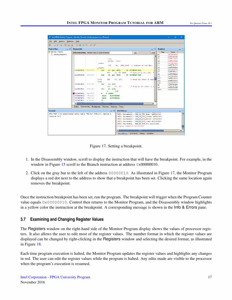
Figure 17. Setting a breakpoint.
1. In the Disassembly window, scroll to display the instruction that will have the breakpoint. For example, in thewindow in Figure 15 scroll to the Branch instruction at address 0x00000010.
2. Click on the gray bar to the left of the address 00000010. As illustrated in Figure 17, the Monitor Programdisplays a red dot next to the address to show that a breakpoint has been set. Clicking the same location againremoves the breakpoint.
Once the instruction breakpoint has been set, run the program. The breakpoint will trigger when the Program Countervalue equals 0x00000010. Control then returns to the Monitor Program, and the Disassembly window highlightsin a yellow color the instruction at the breakpoint. A corresponding message is shown in the Info & Errors pane.
3.7 Examining and Changing Register Values
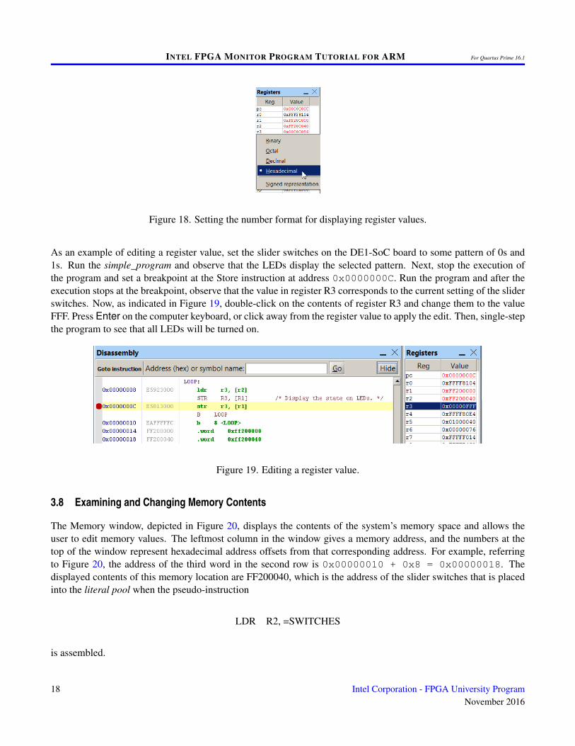
The Registers window on the right-hand side of the Monitor Program display shows the values of processor regis-ters. It also allows the user to edit most of the register values. The number format in which the register values aredisplayed can be changed by right-clicking in the Registers window and selecting the desired format, as illustratedin Figure 18.
Each time program execution is halted, the Monitor Program updates the register values and highlights any changesin red. The user can edit the register values while the program is halted. Any edits made are visible to the processorwhen the program’s execution is resumed.
Intel Corporation - FPGA University ProgramNovember 2016
17
INTEL FPGA MONITOR PROGRAM TUTORIAL FOR ARM For Quartus Prime 16.1
Figure 18. Setting the number format for displaying register values.
As an example of editing a register value, set the slider switches on the DE1-SoC board to some pattern of 0s and1s. Run the simple_program and observe that the LEDs display the selected pattern. Next, stop the execution ofthe program and set a breakpoint at the Store instruction at address 0x0000000C. Run the program and after theexecution stops at the breakpoint, observe that the value in register R3 corresponds to the current setting of the sliderswitches. Now, as indicated in Figure 19, double-click on the contents of register R3 and change them to the valueFFF. Press Enter on the computer keyboard, or click away from the register value to apply the edit. Then, single-stepthe program to see that all LEDs will be turned on.
Figure 19. Editing a register value.
3.8 Examining and Changing Memory Contents
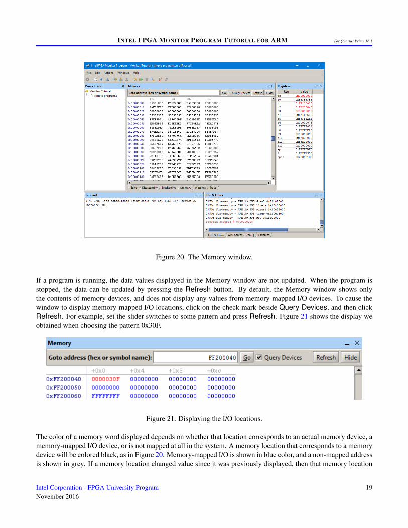
The Memory window, depicted in Figure 20, displays the contents of the system’s memory space and allows theuser to edit memory values. The leftmost column in the window gives a memory address, and the numbers at thetop of the window represent hexadecimal address offsets from that corresponding address. For example, referringto Figure 20, the address of the third word in the second row is 0x00000010 + 0x8 = 0x00000018. Thedisplayed contents of this memory location are FF200040, which is the address of the slider switches that is placedinto the literal pool when the pseudo-instruction
LDR R2, =SWITCHES
is assembled.
18 Intel Corporation - FPGA University ProgramNovember 2016
INTEL FPGA MONITOR PROGRAM TUTORIAL FOR ARM For Quartus Prime 16.1
Figure 20. The Memory window.
If a program is running, the data values displayed in the Memory window are not updated. When the program isstopped, the data can be updated by pressing the Refresh button. By default, the Memory window shows onlythe contents of memory devices, and does not display any values from memory-mapped I/O devices. To cause thewindow to display memory-mapped I/O locations, click on the check mark beside Query Devices, and then clickRefresh. For example, set the slider switches to some pattern and press Refresh. Figure 21 shows the display weobtained when choosing the pattern 0x30F.
Figure 21. Displaying the I/O locations.
The color of a memory word displayed depends on whether that location corresponds to an actual memory device, amemory-mapped I/O device, or is not mapped at all in the system. A memory location that corresponds to a memorydevice will be colored black, as in Figure 20. Memory-mapped I/O is shown in blue color, and a non-mapped addressis shown in grey. If a memory location changed value since it was previously displayed, then that memory location
Intel Corporation - FPGA University ProgramNovember 2016
19

INTEL FPGA MONITOR PROGRAM TUTORIAL FOR ARM For Quartus Prime 16.1
is shown in a red color, as in Figure 21.
Similar to the Disassembly window, it is possible to view different memory regions by scrolling using the verticalscroll bar on the right, or by using a mouse scroll wheel. There is also a Goto address panel, which is analogous tothe Goto instruction panel discussed in Section 3.4. Note that in Figure 21 we reached the I/O device by typing theaddress FF200040 in this panel.
As an example of editing a memory value, go to address FF200000 which is the address of LEDs. Double-click onthe memory word at this address and type the data value FFF. Press Enter on the computer keyboard, or click awayfrom the memory word to apply the edit. This should cause all LEDs to be turned on.
When accessing an I/O device, some reads may be destructive. Namely, after some register in the I/O interface isread, its contents may no longer be valid. Therefore, it is not appropriate to read all I/O registers when refreshingthe information in the Memory window. Instead, it is prudent to read only the registers that are of specific interest.This can be accomplished by left-clicking on the address of interest, then right-clicking and then selecting ReadSelected Address Range to update the displayed contents. Several consecutive addresses can be selected byclicking on the first address and dragging across the other addresses.
It is possible to change the appearance of the Memory window in a number of ways, such as displaying data asbytes, half-words or words. The Memory window provides additional features that are described in more detail inAppendix A of this tutorial.
4 Working with Project Files
Project files store the settings for a particular project, such as the specification of a hardware system and programsource files. A project file, which has the filename extension .amp, is stored into a project’s directory when theproject is created.
The Monitor Program provides the following commands, under the File menu, for working with project files:
1. New Project: Presents a series of screens that are used to create a new project.
2. Open Project: Displays a dialog to select an existing project file and loads the project.
3. Open Recent Project: Displays the five most recently used project files, and allows these projects to bereopened.
4. Save Project: Saves the current project’s settings after they have been modified by using the Settings com-mand.
4.1 Modifying the Settings of an Existing Project
After a project has been created, it is possible to modify many of its settings, if needed. This can be done by clicking
on the menu item Settings > System Settings in the Monitor Program, or the icon. This action will displaythe existing system settings for the project, and allow them to be changed. Similarly, the program settings for the
20 Intel Corporation - FPGA University ProgramNovember 2016
INTEL FPGA MONITOR PROGRAM TUTORIAL FOR ARM For Quartus Prime 16.1
project can be displayed and modified by using the command Settings > Program Settings, or the icon. Tochange these settings, the Monitor Program has to first be disconnected from the system being debugged. This can
be done by using the command Actions > Disconnect, or clicking the icon.
5 Using the Terminal Window
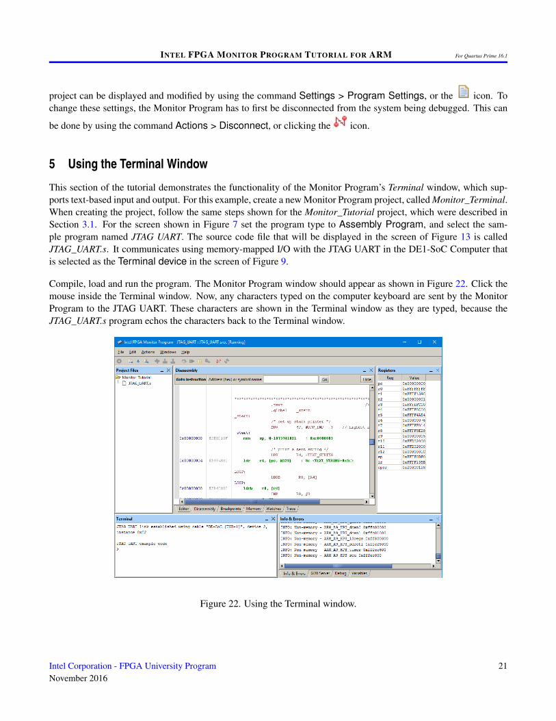
This section of the tutorial demonstrates the functionality of the Monitor Program’s Terminal window, which sup-ports text-based input and output. For this example, create a new Monitor Program project, called Monitor_Terminal.When creating the project, follow the same steps shown for the Monitor_Tutorial project, which were described inSection 3.1. For the screen shown in Figure 7 set the program type to Assembly Program, and select the sam-ple program named JTAG UART. The source code file that will be displayed in the screen of Figure 13 is calledJTAG_UART.s. It communicates using memory-mapped I/O with the JTAG UART in the DE1-SoC Computer thatis selected as the Terminal device in the screen of Figure 9.
Compile, load and run the program. The Monitor Program window should appear as shown in Figure 22. Click themouse inside the Terminal window. Now, any characters typed on the computer keyboard are sent by the MonitorProgram to the JTAG UART. These characters are shown in the Terminal window as they are typed, because theJTAG_UART.s program echos the characters back to the Terminal window.
Figure 22. Using the Terminal window.
Intel Corporation - FPGA University ProgramNovember 2016
21

INTEL FPGA MONITOR PROGRAM TUTORIAL FOR ARM For Quartus Prime 16.1
The Terminal window supports a subset of the control character commands used for a de facto standard terminal,called the VT100. The supported commands are listed in Table 1. In this table <ESC> represents the ASCII characterwith the code 0x1B.
Character Sequence Description<ESC>[2J Erases everything in the Terminal window<ESC>[7h Enable line wrap mode<ESC>[7l Disable line wrap mode<ESC>[#A Move cursor up by # rows or by one row if # is not specified<ESC>[#B Move cursor down by # rows or by one row if # is not specified<ESC>[#C Move cursor right by # columns or by one column if # is not spec-
ified<ESC>[#D Move cursor left by # columns or by one column if # is not speci-
fied<ESC>[#1;#2f Move the cursor to row #1 and column #2
<ESC>[H Move the cursor to the home position (row 0 and column 0)<ESC>[s Save the current cursor position<ESC>[u Restore the cursor to the previously saved position<ESC>[7 Same as <ESC>[s<ESC>[8 Same as <ESC>[u<ESC>[K Erase from current cursor position to the end of the line<ESC>[1K Erase from current cursor position to the start of the line<ESC>[2K Erase entire line<ESC>[J Erase from current line to the bottom of the screen<ESC>[1J Erase from current cursor position to the top of the screen<ESC>[6n Queries the cursor position. A reply is sent back in the format
<ESC>[#1;#2R, corresponding to row #1 and column #2.
Table 1. VT100 commands supported by the Terminal window.
In addition to the JTAG_UART, there exists another option for the terminal device. In Figure 9, in the Terminaldevice dropdown menu there is also a Semihosting option that is useful when C programs are used, as explainedin the next section.
22 Intel Corporation - FPGA University ProgramNovember 2016
INTEL FPGA MONITOR PROGRAM TUTORIAL FOR ARM For Quartus Prime 16.1
6 Using C Programs
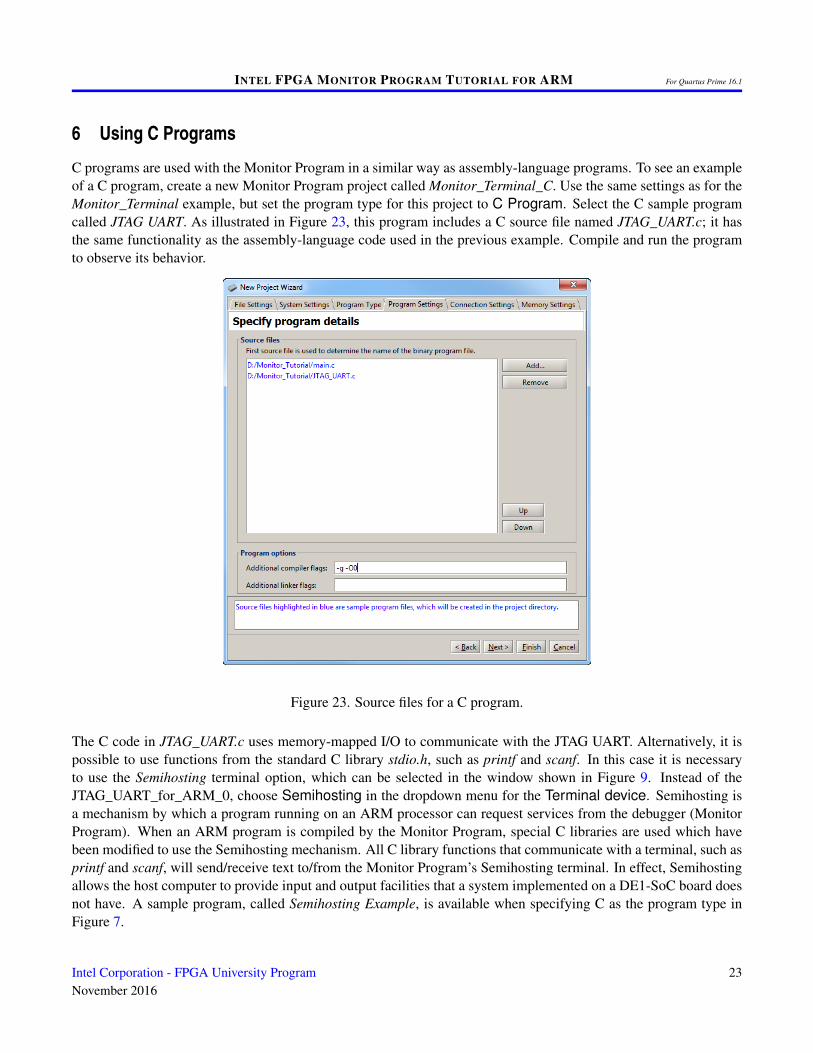
C programs are used with the Monitor Program in a similar way as assembly-language programs. To see an exampleof a C program, create a new Monitor Program project called Monitor_Terminal_C. Use the same settings as for theMonitor_Terminal example, but set the program type for this project to C Program. Select the C sample programcalled JTAG UART. As illustrated in Figure 23, this program includes a C source file named JTAG_UART.c; it hasthe same functionality as the assembly-language code used in the previous example. Compile and run the programto observe its behavior.
Figure 23. Source files for a C program.
The C code in JTAG_UART.c uses memory-mapped I/O to communicate with the JTAG UART. Alternatively, it ispossible to use functions from the standard C library stdio.h, such as printf and scanf. In this case it is necessaryto use the Semihosting terminal option, which can be selected in the window shown in Figure 9. Instead of theJTAG_UART_for_ARM_0, choose Semihosting in the dropdown menu for the Terminal device. Semihosting isa mechanism by which a program running on an ARM processor can request services from the debugger (MonitorProgram). When an ARM program is compiled by the Monitor Program, special C libraries are used which havebeen modified to use the Semihosting mechanism. All C library functions that communicate with a terminal, such asprintf and scanf, will send/receive text to/from the Monitor Program’s Semihosting terminal. In effect, Semihostingallows the host computer to provide input and output facilities that a system implemented on a DE1-SoC board doesnot have. A sample program, called Semihosting Example, is available when specifying C as the program type inFigure 7.
Intel Corporation - FPGA University ProgramNovember 2016
23
INTEL FPGA MONITOR PROGRAM TUTORIAL FOR ARM For Quartus Prime 16.1
6.1 Source Level Debugging
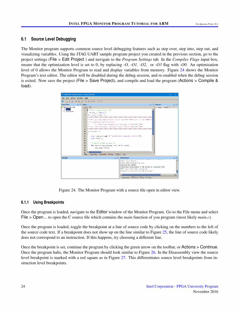
The Monitor program supports common source level debugging features such as step over, step into, step out, andvisualizing variables. Using the JTAG UART sample program project you created in the previous section, go to theproject settings (File > Edit Project ) and navigate to the Program Settings tab. In the Compiler Flags input box,ensure that the optimization level is set to 0, by replacing -O, -O1, -O2, or -O3 flag with -O0. An optimizationlevel of 0 allows the Monitor Program to read and display variables from memory. Figure 24 shows the MonitorProgram’s text editor. The editor will be disabled during the debug session, and re-enabled when the debug sessionis exited. Now save the project (File > Save Project), and compile and load the program (Actions > Compile &load).
Figure 24. The Monitor Program with a source file open in editor view.
6.1.1 Using Breakpoints
Once the program is loaded, navigate to the Editor window of the Monitor Program. Go to the File menu and selectFile > Open... to open the C source file which contains the main function of you program (most likely main.c).
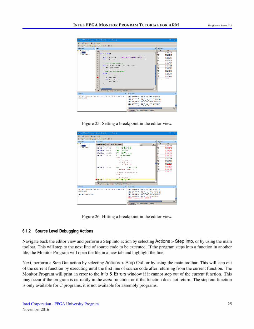
Once the program is loaded, toggle the breakpoint at a line of source code by clicking on the numbers to the left ofthe source code text. If a breakpoint does not show up on the line similar to Figure 25, the line of source code likelydoes not correspond to an instruction. If this happens, try choosing a different line.
Once the breakpoint is set, continue the program by clicking the green arrow on the toolbar, or Actions > Continue.Once the program halts, the Monitor Program should look similar to Figure 26. In the Disassembly view the sourcelevel breakpoint is marked with a red square as in Figure 27. This differentiates source level breakpoints from in-struction level breakpoints.
24 Intel Corporation - FPGA University ProgramNovember 2016
INTEL FPGA MONITOR PROGRAM TUTORIAL FOR ARM For Quartus Prime 16.1
Figure 25. Setting a breakpoint in the editor view.
Figure 26. Hitting a breakpoint in the editor view.
6.1.2 Source Level Debugging Actions
Navigate back the editor view and perform a Step Into action by selecting Actions > Step Into, or by using the maintoolbar. This will step to the next line of source code to be executed. If the program steps into a function in anotherfile, the Monitor Program will open the file in a new tab and highlight the line.
Next, perform a Step Out action by selecting Actions > Step Out, or by using the main toolbar. This will step outof the current function by executing until the first line of source code after returning from the current function. TheMonitor Program will print an error to the Info & Errors window if it cannot step out of the current function. Thismay occur if the program is currently in the main function, or if the function does not return. The step out functionis only available for C programs, it is not available for assembly programs.
Intel Corporation - FPGA University ProgramNovember 2016
25
INTEL FPGA MONITOR PROGRAM TUTORIAL FOR ARM For Quartus Prime 16.1
Figure 27. Source level breakpoint in the disassembly view.
Figure 28. Step Over, Step Into, Step Out toolbar icons
The Step Over action (Actions > Step Over) moves to the next line of source code without stepping into functions.Execution will continue to the next line of source code inside the current function.
6.1.3 Variable Values
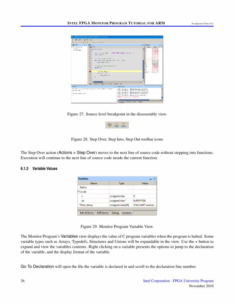
Figure 29. Monitor Program Variable View.
The Monitor Program’s Variables view displays the value of C program variables when the program is halted. Somevariable types such as Arrays, Typedefs, Structures and Unions will be expandable in the view. Use the + button toexpand and view the variables contents. Right clicking on a variable presents the options to jump to the declarationof the variable, and the display format of the variable.
Go To Declaration will open the file the variable is declared in and scroll to the declaration line number.
26 Intel Corporation - FPGA University ProgramNovember 2016
INTEL FPGA MONITOR PROGRAM TUTORIAL FOR ARM For Quartus Prime 16.1
Display As... will change the format in which the variable is displayed.
Variable values are only available with an optimization level of 0 (gcc command line argument -O0). For instructionson how to change the programs optimization level, see the first paragraph of this section.
6.1.4 Enabling and Disabling Source Level Debugging
The source level debugging feature of the Monitor Program is a beta feature in the current release. The featurecan be enabled and disabled at any point by going to the Edit menu and selecting Edit > Enable Source LevelDebugging, or Edit > Disable Source Level Debugging, depending on whether the feature is currently disabledor enabled respectively.
6.1.5 Setting the Optimization Level in Programs with Driver Support.
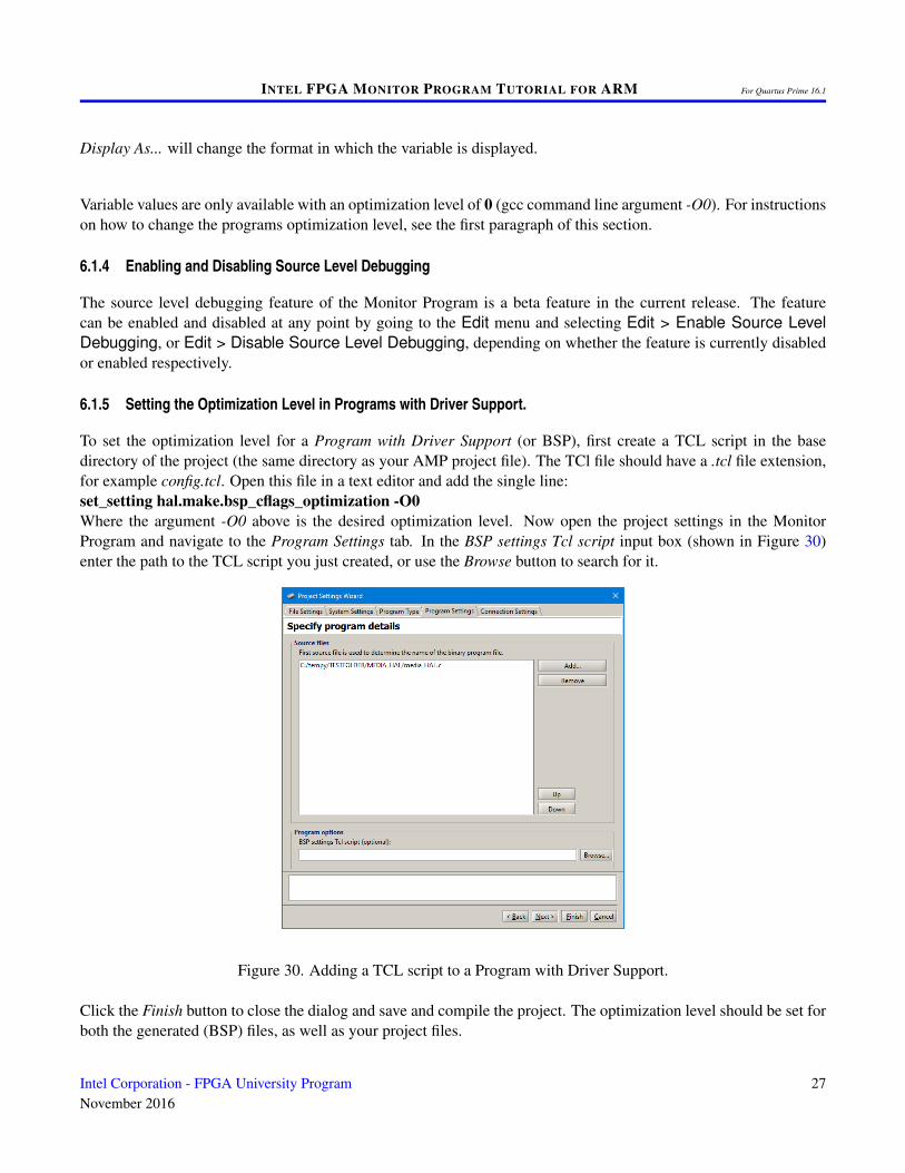
To set the optimization level for a Program with Driver Support (or BSP), first create a TCL script in the basedirectory of the project (the same directory as your AMP project file). The TCl file should have a .tcl file extension,for example config.tcl. Open this file in a text editor and add the single line:set_setting hal.make.bsp_cflags_optimization -O0Where the argument -O0 above is the desired optimization level. Now open the project settings in the MonitorProgram and navigate to the Program Settings tab. In the BSP settings Tcl script input box (shown in Figure 30)enter the path to the TCL script you just created, or use the Browse button to search for it.
Figure 30. Adding a TCL script to a Program with Driver Support.
Click the Finish button to close the dialog and save and compile the project. The optimization level should be set forboth the generated (BSP) files, as well as your project files.
Intel Corporation - FPGA University ProgramNovember 2016
27
INTEL FPGA MONITOR PROGRAM TUTORIAL FOR ARM For Quartus Prime 16.1
7 Using the Monitor Program with Interrupts
The Monitor Program supports the use of exceptions and interrupts in programs. In an ARM-based system, interruptrequests are handled by the Generic Interrupt Controller. Consult the tutorial Using the ARM Generic InterruptController, which is available at the Intel website, for a description of how interrupts are processed.
7.1 Interrupts with Assembly-Language Programs
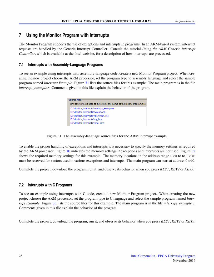
To see an example using interrupts with assembly-language code, create a new Monitor Program project. When cre-ating the new project choose the ARM processor, set the program type to assembly language and select the sampleprogram named Interrupt Example. Figure 31 lists the source files for this example. The main program is in the fileinterrupt_example.s. Comments given in this file explain the behavior of the program.
Figure 31. The assembly-language source files for the ARM interrupt example.
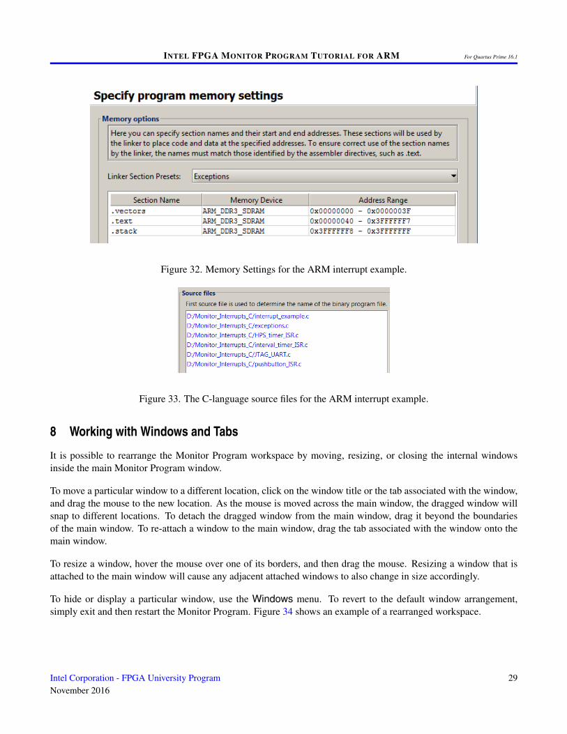
To enable the proper handling of exceptions and interrupts it is necessary to specify the memory settings as requiredby the ARM processor. Figure 10 indicates the memory settings if exceptions and interrupts are not used. Figure 32shows the required memory settings for this example. The memory locations in the address range 0x0 to to 0x3Fmust be reserved for vectors used in various exceptions and interrupts. The main program can start at address 0x40.
Complete the project, download the program, run it, and observe its behavior when you press KEY1, KEY2 or KEY3.
7.2 Interrupts with C Programs
To see an example using interrupts with C code, create a new Monitor Program project. When creating the newproject choose the ARM processor, set the program type to C language and select the sample program named Inter-rupt Example. Figure 33 lists the source files for this example. The main program is in the file interrupt_example.c.Comments given in this file explain the behavior of the program.
Complete the project, download the program, run it, and observe its behavior when you press KEY1, KEY2 or KEY3.
28 Intel Corporation - FPGA University ProgramNovember 2016
INTEL FPGA MONITOR PROGRAM TUTORIAL FOR ARM For Quartus Prime 16.1
Figure 32. Memory Settings for the ARM interrupt example.
Figure 33. The C-language source files for the ARM interrupt example.
8 Working with Windows and Tabs
It is possible to rearrange the Monitor Program workspace by moving, resizing, or closing the internal windowsinside the main Monitor Program window.
To move a particular window to a different location, click on the window title or the tab associated with the window,and drag the mouse to the new location. As the mouse is moved across the main window, the dragged window willsnap to different locations. To detach the dragged window from the main window, drag it beyond the boundariesof the main window. To re-attach a window to the main window, drag the tab associated with the window onto themain window.
To resize a window, hover the mouse over one of its borders, and then drag the mouse. Resizing a window that isattached to the main window will cause any adjacent attached windows to also change in size accordingly.
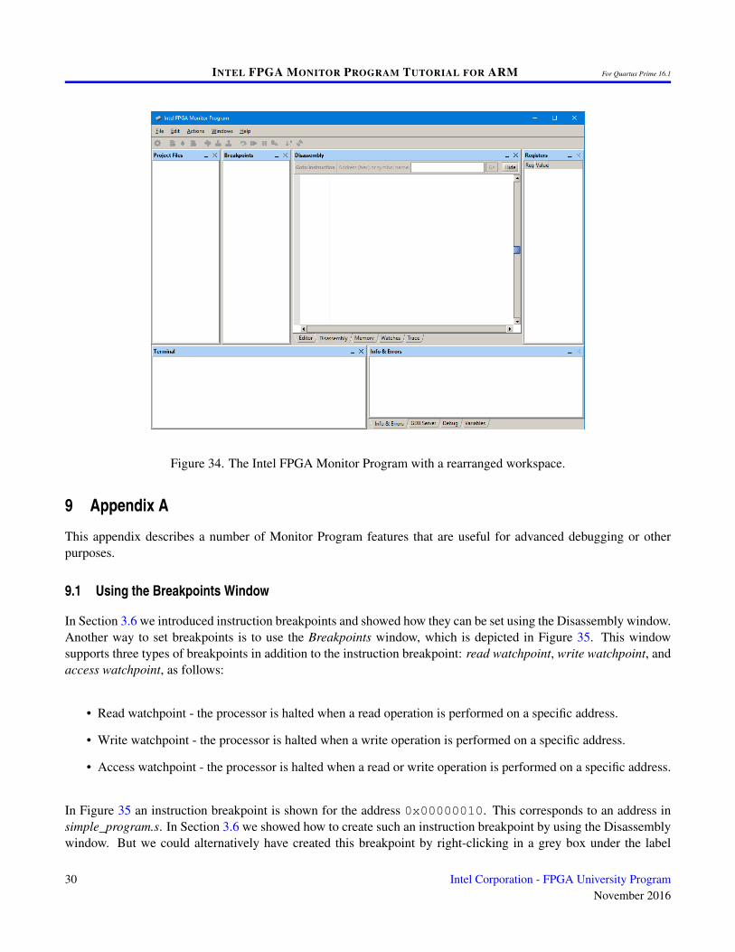
To hide or display a particular window, use the Windows menu. To revert to the default window arrangement,simply exit and then restart the Monitor Program. Figure 34 shows an example of a rearranged workspace.
Intel Corporation - FPGA University ProgramNovember 2016
29
INTEL FPGA MONITOR PROGRAM TUTORIAL FOR ARM For Quartus Prime 16.1
Figure 34. The Intel FPGA Monitor Program with a rearranged workspace.
9 Appendix A
This appendix describes a number of Monitor Program features that are useful for advanced debugging or otherpurposes.
9.1 Using the Breakpoints Window
In Section 3.6 we introduced instruction breakpoints and showed how they can be set using the Disassembly window.Another way to set breakpoints is to use the Breakpoints window, which is depicted in Figure 35. This windowsupports three types of breakpoints in addition to the instruction breakpoint: read watchpoint, write watchpoint, andaccess watchpoint, as follows:
• Read watchpoint - the processor is halted when a read operation is performed on a specific address.
• Write watchpoint - the processor is halted when a write operation is performed on a specific address.
• Access watchpoint - the processor is halted when a read or write operation is performed on a specific address.
In Figure 35 an instruction breakpoint is shown for the address 0x00000010. This corresponds to an address insimple_program.s. In Section 3.6 we showed how to create such an instruction breakpoint by using the Disassemblywindow. But we could alternatively have created this breakpoint by right-clicking in a grey box under the label
30 Intel Corporation - FPGA University ProgramNovember 2016

INTEL FPGA MONITOR PROGRAM TUTORIAL FOR ARM For Quartus Prime 16.1
Figure 35. The Breakpoints window.
Instruction breakpoint in Figure 35 and then selecting Add. A breakpoint can be deleted by unchecking the boxbeside its address.
Setting a read, write, or access watchpoint is done by right-clicking on the appropriate box in Figure 35 and speci-fying the desired address.
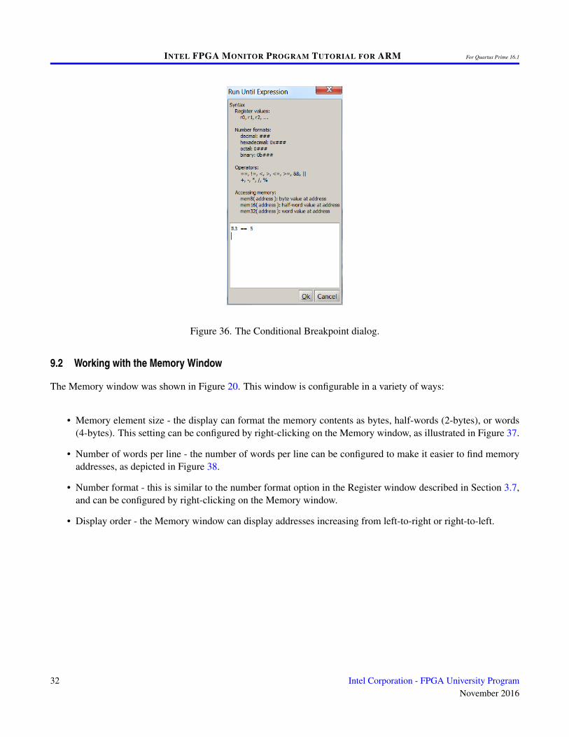
The Monitor Program also supports a type of breakpoint called a conditional breakpoint, which triggers only whena user-specified condition is met. This type of breakpoint is specified in the Run until section by double-clicking onthe empty box under the label Condition in Figure 35 to open the dialog shown in Figure 36. The condition can beassociated with an instructionbreakpoint, or it can be a stand-alone condition if entered inthe Run until box in theBreakpoints window. As an example, we compiled and loaded the simple_program project. Then, we entered thecondition R3 == 5. The condition causes the breakpoint to trigger only if register R3 contains the value 5. Thus,running this program causes the LEDs to display the current state of the slider switches as these switches are set todifferent patterns. But, when the selected pattern is 0x005, the conditional breakpoint will stop the execution of theprogram.
Note that if a stand-alone condition is entered in the Run until box, then the Run button associated with this boxmust be used to run the program, rather than the normal Actions > Continue command. The processor runs muchmore slowly than in its normal execution mode when a conditional breakpoint is being used.
Intel Corporation - FPGA University ProgramNovember 2016
31
INTEL FPGA MONITOR PROGRAM TUTORIAL FOR ARM For Quartus Prime 16.1
Figure 36. The Conditional Breakpoint dialog.
9.2 Working with the Memory Window
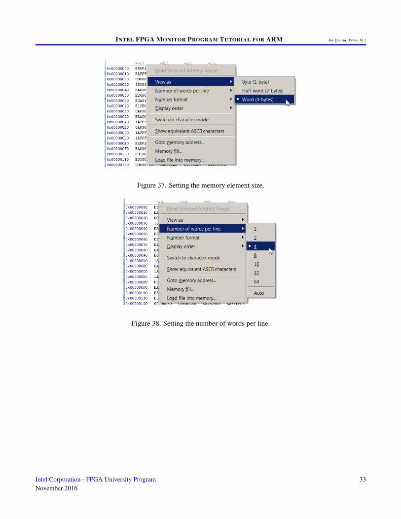
The Memory window was shown in Figure 20. This window is configurable in a variety of ways:
• Memory element size - the display can format the memory contents as bytes, half-words (2-bytes), or words(4-bytes). This setting can be configured by right-clicking on the Memory window, as illustrated in Figure 37.
• Number of words per line - the number of words per line can be configured to make it easier to find memoryaddresses, as depicted in Figure 38.
• Number format - this is similar to the number format option in the Register window described in Section 3.7,and can be configured by right-clicking on the Memory window.
• Display order - the Memory window can display addresses increasing from left-to-right or right-to-left.
32 Intel Corporation - FPGA University ProgramNovember 2016
INTEL FPGA MONITOR PROGRAM TUTORIAL FOR ARM For Quartus Prime 16.1
Figure 37. Setting the memory element size.
Figure 38. Setting the number of words per line.
Intel Corporation - FPGA University ProgramNovember 2016
33
INTEL FPGA MONITOR PROGRAM TUTORIAL FOR ARM For Quartus Prime 16.1
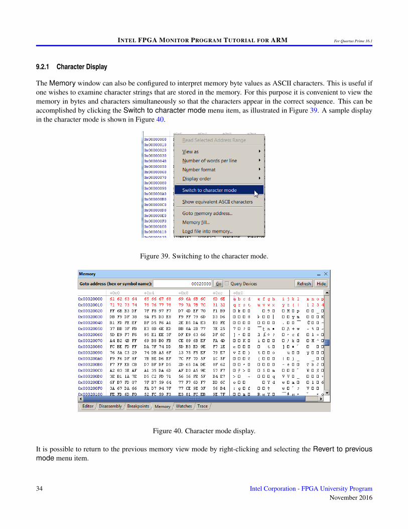
9.2.1 Character Display
The Memory window can also be configured to interpret memory byte values as ASCII characters. This is useful ifone wishes to examine character strings that are stored in the memory. For this purpose it is convenient to view thememory in bytes and characters simultaneously so that the characters appear in the correct sequence. This can beaccomplished by clicking the Switch to character mode menu item, as illustrated in Figure 39. A sample displayin the character mode is shown in Figure 40.
Figure 39. Switching to the character mode.
Figure 40. Character mode display.
It is possible to return to the previous memory view mode by right-clicking and selecting the Revert to previousmode menu item.
34 Intel Corporation - FPGA University ProgramNovember 2016

INTEL FPGA MONITOR PROGRAM TUTORIAL FOR ARM For Quartus Prime 16.1
9.2.2 Memory Fill
Memory fills can be performed in the Memory window. Click the Actions > Memory fill menu item or right-clickon the Memory window and select Memory fill. A Memory fill panel will appear on the left side of the Memorywindow. Simply fill in the desired values and click Fill.
9.2.3 Load File Data into Memory
Data stored in a file can be loaded into the memory by using the Memory window. This feature is accessed byselecting the command Actions > Load file into memory or by right-clicking on the Memory window. The Loadfile panel will appear on the left side of the Memory window, as illustrated in Figure 41, to allow the user to browseand select a data file. The user provides a base address in memory where the data should be stored.
Figure 41. The Load file panel.
The format of these files is illustrated in Figure 42. The file consists of any number of lines, where each linecomprises a comma-separated list of data values. Each data value is expressed as a hexadecimal number with anoptional − sign. Two additional parameters can be specified: the value of the delimiter character (comma is thedefault), and size in bytes of each data value (1 is the default).
Intel Corporation - FPGA University ProgramNovember 2016
35
INTEL FPGA MONITOR PROGRAM TUTORIAL FOR ARM For Quartus Prime 16.1
Figure 42. A Delimited hexadecimal value file.
9.3 Setting a Watch Expression
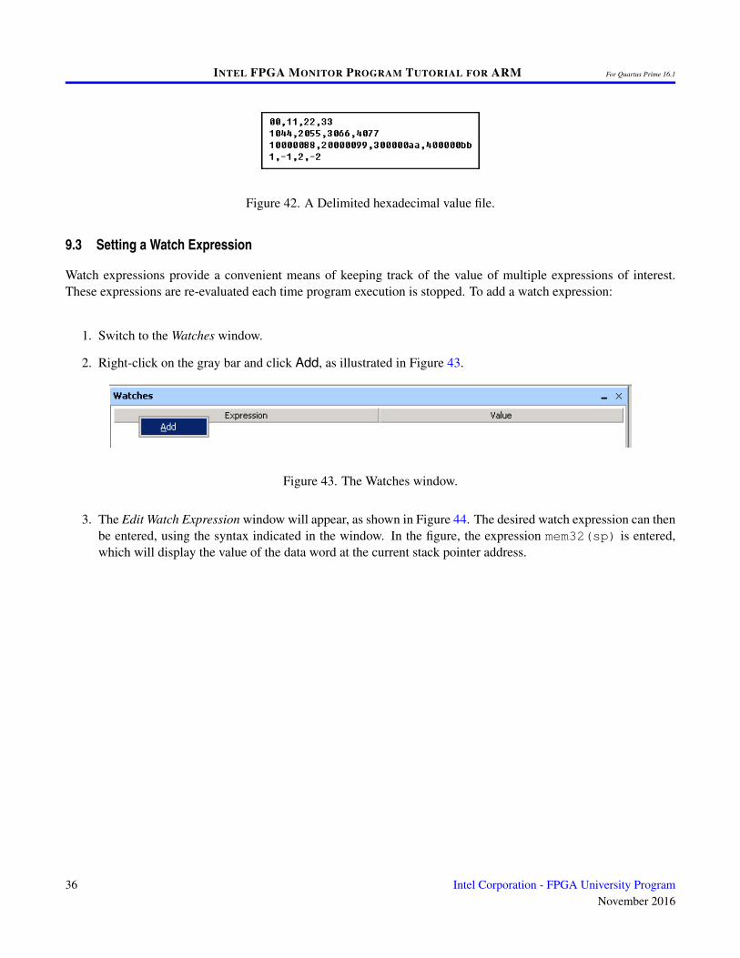
Watch expressions provide a convenient means of keeping track of the value of multiple expressions of interest.These expressions are re-evaluated each time program execution is stopped. To add a watch expression:
1. Switch to the Watches window.
2. Right-click on the gray bar and click Add, as illustrated in Figure 43.
Figure 43. The Watches window.
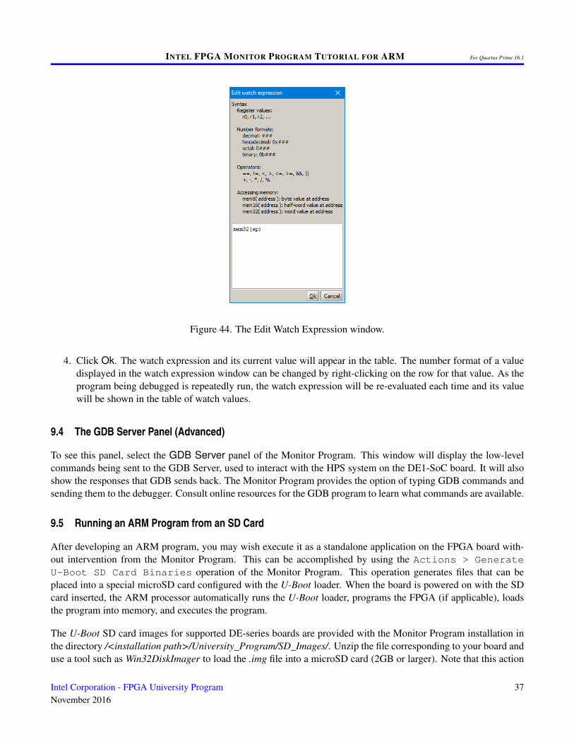
3. The Edit Watch Expression window will appear, as shown in Figure 44. The desired watch expression can thenbe entered, using the syntax indicated in the window. In the figure, the expression mem32(sp) is entered,which will display the value of the data word at the current stack pointer address.
36 Intel Corporation - FPGA University ProgramNovember 2016
INTEL FPGA MONITOR PROGRAM TUTORIAL FOR ARM For Quartus Prime 16.1
Figure 44. The Edit Watch Expression window.
4. Click Ok. The watch expression and its current value will appear in the table. The number format of a valuedisplayed in the watch expression window can be changed by right-clicking on the row for that value. As theprogram being debugged is repeatedly run, the watch expression will be re-evaluated each time and its valuewill be shown in the table of watch values.
9.4 The GDB Server Panel (Advanced)
To see this panel, select the GDB Server panel of the Monitor Program. This window will display the low-levelcommands being sent to the GDB Server, used to interact with the HPS system on the DE1-SoC board. It will alsoshow the responses that GDB sends back. The Monitor Program provides the option of typing GDB commands andsending them to the debugger. Consult online resources for the GDB program to learn what commands are available.
9.5 Running an ARM Program from an SD Card
After developing an ARM program, you may wish execute it as a standalone application on the FPGA board with-out intervention from the Monitor Program. This can be accomplished by using the Actions > GenerateU-Boot SD Card Binaries operation of the Monitor Program. This operation generates files that can beplaced into a special microSD card configured with the U-Boot loader. When the board is powered on with the SDcard inserted, the ARM processor automatically runs the U-Boot loader, programs the FPGA (if applicable), loadsthe program into memory, and executes the program.
The U-Boot SD card images for supported DE-series boards are provided with the Monitor Program installation inthe directory /<installation path>/University_Program/SD_Images/. Unzip the file corresponding to your board anduse a tool such as Win32DiskImager to load the .img file into a microSD card (2GB or larger). Note that this action
Intel Corporation - FPGA University ProgramNovember 2016
37
INTEL FPGA MONITOR PROGRAM TUTORIAL FOR ARM For Quartus Prime 16.1
will remove any existing data in the SD card. Once the SD card has been loaded with the image, it will contain thefollowing files:
• program.bin
• setup_environment.bin
• fpga.rbf
• set_vbar.bin
The files program.bin, setup_environment.bin, and fpga.rbf are generated by the Actions > Generate U-BootSD Card Binaries operation, and together they represent a Monitor Program project. The file program.bin isthe compiled ARM program, setup_environment.bin is a file that contains project configuration details, and fpga.rbfis the FPGA programming file used by the project. All of these files except fpga.rbf are mandatory for successfulexecution (fpga.rbf may be omitted if the project does not use the FPGA). The default files included in the SD cardimage correspond to the Getting Started sample program bundled with the Monitor Program. The file set_vbar.binis a program that is part of the boot sequence that you must not modify nor delete.
To place your own ARM application into the SD card, generate program.bin, setup_environment.bin, and fpga.rbf foryour project by selecting Actions > Generate U-Boot SD Card Binaries in the Monitor Program.Copy over the files to the SD card and replace any prior copies.
10 Appendix B - Configuration File
The Monitor Program configuration file allows default values to be set for project creation. The monitor programsearches $(UniversityProgramRoot)/amp.config for the configuration file, where UniversityProgramRoot is thepath to the University Program directory in the Quartus installation.For example C:/intelFPGA/16.1/University_Program/amp.config.
To change the default path to the configuration file, add the following command line argument when running theMonitor Program: --config-file=<Path to File>
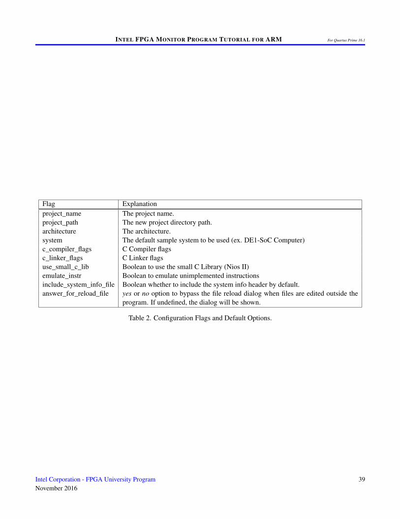
Table 2 summarizes the configuration options available in the Monitor Program.
The configuration file uses white space or an equal sign as a delimiter, for example: flag option or flag=option.Where flag is one of the values in the first column of Table 2 and option is the default value for that flag. Numbersigns (#) can be used to add comments to the configuration file. Lines starting with the symbol will not be processedwith the configuration file. Boolean values can use integers or case insensitive strings. Options of ’false’, ’no’ and’0’ will all produce a false Boolean, any other values will produce a true Boolean.
38 Intel Corporation - FPGA University ProgramNovember 2016
INTEL FPGA MONITOR PROGRAM TUTORIAL FOR ARM For Quartus Prime 16.1
Flag Explanationproject_name The project name.project_path The new project directory path.architecture The architecture.system The default sample system to be used (ex. DE1-SoC Computer)c_compiler_flags C Compiler flagsc_linker_flags C Linker flagsuse_small_c_lib Boolean to use the small C Library (Nios II)emulate_instr Boolean to emulate unimplemented instructionsinclude_system_info_file Boolean whether to include the system info header by default.answer_for_reload_file yes or no option to bypass the file reload dialog when files are edited outside the
program. If undefined, the dialog will be shown.
Table 2. Configuration Flags and Default Options.
Intel Corporation - FPGA University ProgramNovember 2016
39

INTEL FPGA MONITOR PROGRAM TUTORIAL FOR ARM For Quartus Prime 16.1
Copyright © 1991-2016 Intel Corporation. All rights reserved. Intel, The Programmable Solutions Company, thestylized Intel logo, specific device designations, and all other words and logos that are identified as trademarksand/or service marks are, unless noted otherwise, the trademarks and service marks of Intel Corporation in the U.S.and other countries. All other product or service names are the property of their respective holders. Intel productsare protected under numerous U.S. and foreign patents and pending applications, mask work rights, and copyrights.Intel warrants performance of its semiconductor products to current specifications in accordance with Intel’s stan-dard warranty, but reserves the right to make changes to any products and services at any time without notice. Intelassumes no responsibility or liability arising out of the application or use of any information, product, or servicedescribed herein except as expressly agreed to in writing by Intel Corporation. Intel customers are advised to obtainthe latest version of device specifications before relying on any published information and before placing orders forproducts or services.
This document is being provided on an “as-is” basis and as an accommodation and therefore all warranties, repre-sentations or guarantees of any kind (whether express, implied or statutory) including, without limitation, warrantiesof merchantability, non-infringement, or fitness for a particular purpose, are specifically disclaimed.
40 Intel Corporation - FPGA University ProgramNovember 2016