integrated wavelength division multiplexing receiversintegrated wavelength division multiplexing...
TRANSCRIPT

Integrated wavelength division multiplexing receivers
Citation for published version (APA):Nikoufard, M. (2008). Integrated wavelength division multiplexing receivers. Eindhoven: Technische UniversiteitEindhoven. https://doi.org/10.6100/IR633916
DOI:10.6100/IR633916
Document status and date:Published: 01/01/2008
Document Version:Publisher’s PDF, also known as Version of Record (includes final page, issue and volume numbers)
Please check the document version of this publication:
• A submitted manuscript is the version of the article upon submission and before peer-review. There can beimportant differences between the submitted version and the official published version of record. Peopleinterested in the research are advised to contact the author for the final version of the publication, or visit theDOI to the publisher's website.• The final author version and the galley proof are versions of the publication after peer review.• The final published version features the final layout of the paper including the volume, issue and pagenumbers.Link to publication
General rightsCopyright and moral rights for the publications made accessible in the public portal are retained by the authors and/or other copyright ownersand it is a condition of accessing publications that users recognise and abide by the legal requirements associated with these rights.
• Users may download and print one copy of any publication from the public portal for the purpose of private study or research. • You may not further distribute the material or use it for any profit-making activity or commercial gain • You may freely distribute the URL identifying the publication in the public portal.
If the publication is distributed under the terms of Article 25fa of the Dutch Copyright Act, indicated by the “Taverne” license above, pleasefollow below link for the End User Agreement:www.tue.nl/taverne
Take down policyIf you believe that this document breaches copyright please contact us at:[email protected] details and we will investigate your claim.
Download date: 07. Apr. 2020

Integrated Wavelength Division MultiplexingReceivers


Integrated Wavelength Division MultiplexingReceivers
PROEFSCHRIFT
ter verkrijging van de graad van doctor aan deTechnische Universiteit Eindhoven, op gezag van de
Rector Magnificus, prof.dr.ir. C.J. van Duijn, voor eencommissie aangewezen door het College voor
Promoties in het openbaar te verdedigenop dinsdag 25 maart 2008 om 16.00 uur
door
Mahmoud Nikoufard
geboren te Aran en Bidgol, Iran

Dit proefschrift is goedgekeurd door de promotoren:
prof.dr.ir. M.K. Smitenprof.dr. D. Lenstra
Copromotor:dr. X.J.M. Leijtens
This research was supported by the Dutch Technology FoundationSTW through project DEL66.4203, by the Dutch Ministry of Economic Affairs through the NRC Photonics Grant, by theMinistry of Science, Research, and Technology (Iran), and by Kashan University (Iran).The trans-impedance travelling wave amplifier is designed byTNO-FEL (the Hague, the Nether-lands).
Copyright c© 2008 Mahmoud NikoufardTypeset using LYX, printed in The Netherlands.
CIP-DATA LIBRARY TECHNISCHE UNIVERSITEIT EINDHOVEN
Nikoufard, Mahmoud
Integrated wavelength division multiplexing receivers / by Mahmoud Nikoufard.−Eindhoven : Technische Universiteit Eindhoven, 2008.Proefschrift.− ISBN 978-90-386-1814-2NUR 959Trefw.: optische telecommunicatie / optische detectoren / optische versterkers / geïntegreerdeoptica / multiplexers.Subject headings: optical communication / photodetectors / semiconductor optical amplifiers/ integrated optics / multiplexing.

to my wife, daughters,parents, and parents-in-law


Contents
1 Introduction 11.1 Wavelength division multiplexing. . . . . . . . . . . . . . . . . . . . . . . . 11.2 A comparison of various photodetectors. . . . . . . . . . . . . . . . . . . . . 21.3 An overview to the InP-based demultiplexers. . . . . . . . . . . . . . . . . . 51.4 Monolithic integrated WDM-receiver in InP material: overview. . . . . . . . . 71.5 Thesis outline. . . . . . . . . . . . . . . . . . . . . . . . . . . . . . . . . . . 9
2 Twin-waveguide pin-photodetector 132.1 Introduction. . . . . . . . . . . . . . . . . . . . . . . . . . . . . . . . . . . .132.2 Operation principles. . . . . . . . . . . . . . . . . . . . . . . . . . . . . . . .142.3 Optical and electrical properties of
InGaAs(P)/InP materials. . . . . . . . . . . . . . . . . . . . . . . . . . . . .162.4 Optical and electrical design of the twin-WGPD. . . . . . . . . . . . . . . . . 17
2.4.1 Twin-WGPD structure. . . . . . . . . . . . . . . . . . . . . . . . . .172.4.2 Optical design . . . . . . . . . . . . . . . . . . . . . . . . . . . . . .182.4.3 Optical optimization of the twin-WGPD structure. . . . . . . . . . . . 222.4.4 Electrical design. . . . . . . . . . . . . . . . . . . . . . . . . . . . .23
2.5 Fabrication of the twin-WGPD. . . . . . . . . . . . . . . . . . . . . . . . . .302.5.1 Epitaxial growth . . . . . . . . . . . . . . . . . . . . . . . . . . . . .302.5.2 Processing scheme. . . . . . . . . . . . . . . . . . . . . . . . . . . .30
2.6 Optical and electrical measurements. . . . . . . . . . . . . . . . . . . . . . . 332.6.1 Static characterization. . . . . . . . . . . . . . . . . . . . . . . . . .332.6.2 High-frequency response. . . . . . . . . . . . . . . . . . . . . . . . .352.6.3 Small-signal equivalent-circuit model. . . . . . . . . . . . . . . . . . 38
2.7 Conclusion . . . . . . . . . . . . . . . . . . . . . . . . . . . . . . . . . . . .40
3 Hybrid integration of a MWR and TI-TWA 433.1 Introduction. . . . . . . . . . . . . . . . . . . . . . . . . . . . . . . . . . . .433.2 Design of a polarization independent MWR. . . . . . . . . . . . . . . . . . . 45
3.2.1 Basic AWG-operation principle and design parameters. . . . . . . . . 453.2.2 Polarization dispersion compensation methods. . . . . . . . . . . . . 46
vii

viii Contents
3.2.3 Array arm birefringence compensation. . . . . . . . . . . . . . . . . 483.2.4 Photodetector design. . . . . . . . . . . . . . . . . . . . . . . . . . .50
3.3 Fabrication . . . . . . . . . . . . . . . . . . . . . . . . . . . . . . . . . . . .523.4 Characterization of the optical multi-wavelength receiver. . . . . . . . . . . . 53
3.4.1 Static characterization. . . . . . . . . . . . . . . . . . . . . . . . . .533.4.2 RF-characterization. . . . . . . . . . . . . . . . . . . . . . . . . . . .56
3.5 Design of the trans-impedance traveling-wave amplifier. . . . . . . . . . . . . 633.5.1 Characterization of the trans-impedance traveling-wave amplifier. . . 66
3.6 Mounting and bonding. . . . . . . . . . . . . . . . . . . . . . . . . . . . . .673.7 Hybrid integrated MWR and TI-TWA. . . . . . . . . . . . . . . . . . . . . . 723.8 Conclusion . . . . . . . . . . . . . . . . . . . . . . . . . . . . . . . . . . . .73
4 Waveguide pin-photodetector 754.1 Introduction. . . . . . . . . . . . . . . . . . . . . . . . . . . . . . . . . . . .754.2 WGPD quantum efficiency and bandwidth. . . . . . . . . . . . . . . . . . . . 774.3 Optimization strategy. . . . . . . . . . . . . . . . . . . . . . . . . . . . . . .784.4 Optical and electrical design of the WGPD. . . . . . . . . . . . . . . . . . . . 78
4.4.1 Optical design . . . . . . . . . . . . . . . . . . . . . . . . . . . . . .794.4.2 Electrical design. . . . . . . . . . . . . . . . . . . . . . . . . . . . .824.4.3 Monolithic integration of the WGPD with passive waveguide. . . . . . 86
4.5 Fabrication Technology. . . . . . . . . . . . . . . . . . . . . . . . . . . . . .914.5.1 Epitaxial regrowth . . . . . . . . . . . . . . . . . . . . . . . . . . . .924.5.2 RIE-etch . . . . . . . . . . . . . . . . . . . . . . . . . . . . . . . . .924.5.3 Passivation and planarization with polyimide. . . . . . . . . . . . . . 944.5.4 Metalization . . . . . . . . . . . . . . . . . . . . . . . . . . . . . . .964.5.5 Processing scheme. . . . . . . . . . . . . . . . . . . . . . . . . . . .97
4.6 Characterization. . . . . . . . . . . . . . . . . . . . . . . . . . . . . . . . . .1024.6.1 static measurements. . . . . . . . . . . . . . . . . . . . . . . . . . .1034.6.2 Responsivity and efficiency. . . . . . . . . . . . . . . . . . . . . . .1034.6.3 RF-measurements. . . . . . . . . . . . . . . . . . . . . . . . . . . .104
4.7 Conclusions. . . . . . . . . . . . . . . . . . . . . . . . . . . . . . . . . . . .105
5 Design of a pre-amplified MWR on SI-InP 1075.1 Introduction. . . . . . . . . . . . . . . . . . . . . . . . . . . . . . . . . . . .1075.2 Concept of the pre-amplified MWR. . . . . . . . . . . . . . . . . . . . . . .1085.3 Semiconductor optical amplifiers. . . . . . . . . . . . . . . . . . . . . . . . .1085.4 Sensitivity of the MWR. . . . . . . . . . . . . . . . . . . . . . . . . . . . . .111
5.4.1 Receiver noise. . . . . . . . . . . . . . . . . . . . . . . . . . . . . .1125.4.2 Photodetector shot and thermal noise. . . . . . . . . . . . . . . . . .1145.4.3 SOA noise . . . . . . . . . . . . . . . . . . . . . . . . . . . . . . . .1145.4.4 AWG signal-crosstalk beat noise. . . . . . . . . . . . . . . . . . . . .1165.4.5 Receiver sensitivity. . . . . . . . . . . . . . . . . . . . . . . . . . . .117
5.5 Multi Wavelength Receiver design. . . . . . . . . . . . . . . . . . . . . . . .121

Contents ix
5.5.1 Passive components structure. . . . . . . . . . . . . . . . . . . . . .1215.5.2 SOA design. . . . . . . . . . . . . . . . . . . . . . . . . . . . . . . .1255.5.3 Photodetector . . . . . . . . . . . . . . . . . . . . . . . . . . . . . .1285.5.4 Monolithic integration trade-off. . . . . . . . . . . . . . . . . . . . .128
5.6 Characterization. . . . . . . . . . . . . . . . . . . . . . . . . . . . . . . . . .1295.6.1 InP-based ridge laser with lateral n-contacts. . . . . . . . . . . . . . .1295.6.2 Eight channel MWR. . . . . . . . . . . . . . . . . . . . . . . . . . .132
5.7 Conclusion . . . . . . . . . . . . . . . . . . . . . . . . . . . . . . . . . . . .134
References 137
List of constants, symbols and acronyms 145
Summary 153
Acknowledgements 155
Curriculum Vitæ 157

x Contents

Chapter 1
Introduction
This chapter gives a short introduction to wavelength division multiplexing (WDM) technique.Integrated WDM receivers are key components in future WDM systems. The main elementsof integrated WDM receivers, wavelength demultiplexers and photodetectors are shortly dis-cussed and the contents of the thesis is outlined.
1.1 Wavelength division multiplexing
The rapid expansion of optical communication networks has created a requirement to increasethe transmission capacity of these networks. The high capacity of optical networks basicallydepends on a high-speed transmitter, a high-capacity optical fiber, and a high-speed receiver.To increase the capacity of such networks, several techniques are utilized. One of the mostpopular techniques is wavelength division multiplexing. Figure1.1 schematically shows asimplified WDM link. At the transmitter, a wavelength multiplexer is used to combine themodulated signals of the transmitter lasers operating at various wavelengths. The combinedwavelengths at the multiplexer are launched into the optical fiber and at the receiver the de-multiplexer separates them and couples the light to the photodetectors. With this scheme anultra-wide bandwidth link is possible.
If the modules of aWDM network are built from discrete components, they will be ex-pensive, also because each optical module must be tuned precisely to the correct wavelength.On the other-hand, in order to enable the consumers to get access to broadband services suchas video-telephony and high-density television (HDTV), low cost and high capacityWDM net-works must be developed. Monolithic or hybrid integration of the optical and electronic com-ponents offers a promising path to move toward a high-speed, low-cost, and reliableWDM
network. Hybrid integration of optical-optical or optical-electrical components with differentfabrication technologies offers the advantage of integration of various functionalities realized
1

2 1. Introduction
Figure 1.1: Schematic diagram of a point-to-pointWDM link (MOD=modulator,PD=photodetector, pre-amp=front-end pre-amplifier).
in the most suitable technologies, but it requires additional packaging and bonding opera-tions. Monolithic integration of the optical components offers the advantage of a compact sizethat allows higher integration densities and easy and reliable connection between the differentcomponents. In this thesis, both types of technology are employed: monolithic integration ofseveral optical components in planar technology on semi-insulating InP and hybrid integrationof two chips fabricated with incompatible technologies (optical and electrical in InP and GaAsmaterials, respectively).
Monolithic integration of components in aWDM receiver or transmitter requires a materialthat provides all the required functionality (generation, transmission, and detection of light) inthe operation wavelength window of the link. In the 1.55µm wavelength window, the opticalfiber has the lowest attenuation. For this reason, semiconductor materials operating in thiswindow are attractive to fabricate components forWDM. In1−xGaxAs1−yPy materials lattice-matched to InP cover the entire wavelength range of 0.92-1.65µm and the use of InP/InGaAsPsemiconductor materials for monolithic integration of the optical transmitter or receiver de-vices and is therefore the preferred material in this window. In addition, this material has thecapability of monolithic integration with electronic devices [1–4]. The current thesis is abouta monolithically integratedWDM receiver in InP/InGaAsP material, and its hybrid integrationwith anRF receiver amplifier.
1.2 A comparison of various photodetectors
The most important features of a receiver module are the bandwidth (usually specified as the3 dB bandwidth, i.e. the frequency at which the responsivity is reduced by 3 dB) and the re-ceiver sensitivity (i.e. the minimum detectable power by the receiver). The latter is determinedby the external efficiency, the dark current, and the noise properties of the electronic pream-

1.2 A comparison of various photodetectors 3
plifier that follows the photodetector. The bandwidth-efficiency product is a figure of meritfor photodetectors. Some other essential parameters are: stability of the characteristics withrespect to changes in temperature and voltage, low bias voltage, high reliability, small size,low cost, and high sensitivity at the operating wavelengths [5].
One of the most common types of the photodetector is a vertically illuminated photodetec-tor (VPD), shown schematically in figure1.2-a. In theVPD, light propagates across the depletedintrinsic absorption layer created by the reverse bias voltage. In theVPD, a thick absorptionlayer increases the efficiency and carrier transit time. TheVPD therefore suffers from a trade-off between efficiency and bandwidth. The main advantages ofVPDs are a single epitaxiallayer structure, a simple fabrication process, and easy access to the wide input facet. In thepin-VPD photodetector, the mobility of majority carriers in the n-layer is much larger than inthe p-layer. So, with illuminating the n-side instead of the p-side layer, it is possible to increasethe bandwidth. Tuckeret al.[6] reported a pin-VPD, having a bandwidth of 67 GHz with anexternal quantum efficiency of 27%.
One of the approaches to increase the efficiency of the conventional pin-VPD is utilizingmirrors to reflect the light through the absorbing material several times. This type of photode-tector, as depicted in figure1.2-b, is called resonant-cavity-enhanced (RCE) photodetector. IntheRCE-VPD, the mirrors are Bragg reflectors which effectively increase the absorption length,resulting in an increase of the quantum efficiency (at the cavity center wavelength) without sac-rificing the electrical bandwidth [7]. The resistance of the mirrors limit theRC-bandwidth andthe center wavelength of the cavity shifts with temperature.
The pin-waveguide photodetector (pin-WGPD) is an option to increase the bandwidth-efficiency product. TheWGPD is a side-illuminated photodetector in which the transparentcladding layers and the absorbing (guiding) layer form an optical waveguide (figure1.2-c).The photons enter the photodetector from the side. In theWGPD, a low transit time and a highquantum efficiency is obtained with a thin absorption layer and a long absorption path. Dueto the thin guiding layer, the coupling efficiency is low which can be increased by using aspot-size convertor [8]. The WGPD is well-suited for integration with other optical waveguidecomponents while keeping its performance high in a wide wavelength range. The integrationof the WGPD with passive or active optical components requires an epitaxial regrowth step,which complicates the fabrication process. Wakeet al.[9] reported an InP-basedWGPD with a50 GHz bandwidth and 40% external quantum efficiency.
The evanescent couplingWGPD(or twin-waveguide photodetector) is a good alternative fortheWGPD to avoid epitaxial regrowth. In the evanescently coupledWGPD, the pin-PD structureis grown on top of the passive waveguide (see figure1.2-e). The advantage of this scheme is thatonly single epitaxial growth with a simple fabrication processing is needed. In reference [10],a bandwidth of 70 GHz and 90% internal quantum efficiency at 1.55µm wavelength is re-ported. In reference [11], a tapered twin-guide photodetector with 11 GHz bandwidth and 0.3and 0.55 A/W responsivity for bulk andQW-active layer material, respectively, is reported.
The performance of theWGPD is practically limited by parasitic elements. Decreasing thethickness of the absorption layer results in a reduction of the transit time and an increase ofthe capacitance. A mush-room mesa structure is suggested by Kato [12] to avoid the increaseof the junction capacitance due to the thin absorption layer. In this structure that is shown in

4 1. Introduction
i - t y p e
p - t y p e
n - t y p e
E
L i g h t
i - t y p e
p - t y p e
n - t y p e
E
L i g h t
M i r r o r
(a) (b)
i - t y p e
p - t y p e
n - t y p e
E
L i g h t
i - t y p e
p - t y p e
n - t y p e
E
(c) (d)
L i g h t
g u i d
c l a d
c l a d
n - t y p eE
p - t y p ei - t y p e
(e)
Figure 1.2: The schematic figures of a)VPD, b)RCE-VPD, c)WGPD, d) mush-room mesa,and e) twin-WGPD.

1.3 An overview to the InP-based demultiplexers 5
figure1.2-d, the absorption layer is narrower than the cladding layers, which reduces the junc-tion capacitance. The mush-room mesaWGPD in reference [12] showed 100 GHz bandwidthand 50% external quantum efficiency.
The WGPD suffers from a large impedance mismatch between the photodetector and theload. To overcome the bandwidth limitation of theWGPDand reduce the impedance mismatch,a traveling-wave photodetector has been used [13]. This device is based on theWGPD, but it hasspecial electrodes designed for supporting of a traveling electrical wave, with a characteristicimpedance that is matched to the external load. Giboney [14] modeled and realized aTWPD
with 170 GHz bandwidth and about 50% quantum efficiency. Beling [15] recently reported aperiodic parallel-fedTWPD with 85 GHz bandwidth.
In this work, both a single and a twin-waveguide photodetector are investigated. The mainchallenge for the realization of the twin-WGPD is to design a small area photodetector with anoptimum layer thickness for reaching a high efficiency (more than 90%) and a high bandwidth(e.g. operational for a 40 Gb/s link). In this thesis the focus has been on development of aWGPD which is compatible with the integration technology that is used for realisation of abroad class of devices such asMMI -couplers andAWGs, optical amplifiers (for use as a pre-amplifier) and phase-shifters (for making theAWG tunable).
1.3 An overview to the InP-based demultiplexers
An important component in theWDM-receiver is the wavelength demultiplexer. A wavelengthdemultiplexer is an optical filter, which spatially separates the incoming wavelengths. Un-til now, three different types of de/multiplexers are commercially available [16]: fiber-based,micro-optic, and integrated-optic de/multiplexers. In fiber-based de/multiplexers, a combina-tion of optical filters and fiber splitters offers multi-channel de/multiplexing. Most work onmicro-optic de/multiplexers was carried out in the early eighties by using collimating opticsand reflecting gratings. In the early nineties, integrated optic demultiplexers employedMZI
duplexers. Later on, grating-based devices (AWG and bragg-gratings) were used. In the nextsection, we describe the de/multiplexers that are employed in InP-based photonic integratedcircuits.
Arrayed waveguide grating (AWG )
The AWG∗ is the most common demultiplexer in photonic integrated circuits. AnAWG isa wavelength demultiplexer based on a planar array of waveguides that has been designedsuch that it combines focusing and dispersive properties. With the focusing properties, thelight from an input waveguide is focused onto one of an array of output waveguides. Dueto the dispersive properties of the waveguide array, the focal spot moves to a different outputwaveguide if the wavelength is changed. In this way, the different wavelengths are coupled todifferent output waveguides (see figure1.3-a). The main design parameters of theAWG are the
∗Also known as phased-array (PHASAR) demultiplexer, phased-array waveguide grating (PAWG), waveguide grat-ing router (WGR).

6 1. Introduction
central wavelength, the number of input and output channels, the channel spacing and the freespectral range (FSR). Typical values of the insertion loss and crosstalk for the InP-basedAWG
are about 5 dB and -20dB, respectively.TheAWG demultiplexer device was proposed for the first time by Smit [17] in 1988. Taka-
hashiet al. [18, 19] reported the firstAWG operating in the telecommunication wavelengthwindow. Dragone [20, 21] extended theAWG concept from 1×N to N×N devices. Takahashietal.[22] reported the first polarization independentAWG by using birefringence compensation inthe waveguide array. TheAWG demultiplexer is utilized as a building block in a number of op-tical devices such as multi-wavelength transmitters, add-drop multiplexers, multi-wavelengthreceivers, and wavelength converters [23].
Grating demultiplexer
A grating demultiplexer consists of a mirror surface with tiny periodic grooves. The incidentlight to the surface of the grooves diffracts and causes patterns in the diffracted wave. Theinterference pattern is wavelength dependent and certain wavelengths are only diffracted in agiven diffraction direction. (see figure1.3-b).
Grating demultiplexers usually operate at a low order, offering typically more than 50 nmfree spectral range for the demultiplexing of a large number of wavelength channels. However,the insertion loss depends on the quality of the vertically etched reflection grating mirrorsand the crosstalk depends strongly on the correct position of the grooves. Huet al.[24] havereported a grating demultiplexer with 10 dB insertion loss and−25 dB crosstalk.
Mach-Zehnder interferometer (MZI) demultiplexer
A MZI -demultiplexer consists of twoMMI couplers (a splitter and a combiner) that are con-nected by waveguides of unequal-length. It can be designed such that properly spaced wave-lengths are each routed to a different output waveguide. In figure1.3-c a two-channelMZI
demultiplexer is shown. By cascading 2n−1 MZI demultiplexers, it is possible to realize ann-channel wavelength demultiplexer. InMZI -based demultiplexers, the insertion loss can besmall and crosstalk and fabrication tolerance depend on the number of channels.
A special type of a four channelMZI demultiplexer with twoMMI s and four arms of unequallength is proposed by van Dam [25]. The realized device showed an insertion loss of less than4dB and a crosstalk of−13dB. The cross-talk of this device is very sensitive to width variationsof theMMI -coupler. This type of demultiplexer is only suitable for a small number of channels.
Bragg grating (BG) demultiplexer
This type of demultiplexer consists of a region in the waveguide in which the index of thewaveguide varies periodically. If the light beam couples to the periodic structure, multiplereflections and transmissions occur. For specific wavelengths, the reflected waves are in phaseand total reflection occurs [26] (see figure1.3-d). TheBG can be combined with Y-junction orMMI power splitters to increase the number of demultiplexed channels.

1.4 Monolithic integrated WDM-receiver in InP material: overview 7
Comparison
A comparison among grating-based demultiplexers shows that theAWG has more attractivefeatures for us: a simple fabrication process based on conventional waveguide technology,whereas the grating demultiplexer requires an accurate design in combination with very deepvertical etching (which complicates integration). However, due to the physical size and fab-rication tolerances required to achieve high channel counts and narrow channel spacing inthe AWG demultiplexers, the grating demultiplexer may be deployed for extremely compactphotonic integrated circuits in the future. In theMZI and BG demultiplexers, the length andfabrication tolerance depend on the number of channels, which restrict their use for a lownumber of channels. In addition, in theBG demultiplexer, the output power is attenuated witha factor ofN due to the use of the Y-junctions orMMI -couplers as power splitters.
1.4 Monolithic integrated WDM-receiver in InP material:overview
This section addresses the history of the monolithic integration of theWDM-receivers that usea combination of a demultiplexer, photodetectors, and/or a semiconductor optical amplifier(SOA) on InP substrate for operation at 1.55µm wavelength.
Winzer [27] has reported the first integrated two-channelWDM receiver. TheWDM re-ceiver consisted of aMMI power splitter, twoBG filters, one in each branch of theMMI powersplitter and two pin-photodiodes. The channel spacing of the demultiplexer was 450 GHz,and 420 MHz bandwidth was reported. The external quantum efficiency of the channels andthe dark current were about 8% and 5 nA, respectively. This configuration leads to a 3-dBadditional loss due to theMMI -splitter.
A suitable way to increase the number of channels of theWDM receiver is to use a gratingdemultiplexer orAWG. A WDM receiver with 42 optical channels using a grating demultiplexerwas demonstrated by Cremeret al.[28]. The photodiodes are integrated on top of the outputwaveguides. The device has a 500 GHz channel spacing,−15 dB channel crosstalk, 90% in-ternal quantum efficiency and an external quantum efficiency of 0.008 A/W. The low externalefficiency is mainly caused by the poor quality of the grating. Amersfoortet al.[29] have re-ported the first integrated receiver with anAWG demultiplexer and four photodetectors. Thedevice had 200 GHz channel spacing. The realized device shows a considerable improvementover insertion loss, crosstalk and external responsivity (which are 5dB,−21dB, and 0.12A/W,respectively) with respect to the grating-based receiver in reference [28].
Due to similarity of the structure of theSOA and the photodetector (both use a pin-structurebut operate at forward and reverse bias voltage, respectively), Zirngibl [30] proposed and re-alized the first pre-amplifiedWDM receiver by monolithic integration of a semiconductor op-tical preamplifier, anAWG, and a photodetector array. The characteristics of the receiver are−20 dB crosstalk, 0.5 A/W responsivity, 200 GHz channel spacing, and 3.5 GHz bandwidth.The structure of the pre-amplifiedWDM receiver was the same as used in the multi-wavelengthlaser [31] in which theSOA now served as a photodetector. The first monolithic integration of

8 1. Introduction
l 1 , 2
l 1
l 2
(a) (b)
l 1 , 2 l 2
l 1
i n p u tw a v e g u i d e
o u t p u t w a v e g u i d e s
l 1 , 2l 1
l 2(c) (d)
Figure 1.3: (a) Schematic layout of anAWG demultiplexer. (b) Schematic view of thegrating demultiplexer. (c) Schematic layout of aMZI -demultiplexer. (d) Schematic layoutof a bragg grating demultiplexer.

1.5 Thesis outline 9
a SOA preamplifier, a grating demultiplexer, and pin-photodiodes was reported by Cremeretal. [32]. The crosstalk and responsivity are about−20 dB and 8 A/W, respectively, withoutany information about receiver bandwidth. Later in 1996, they reported a pre-amplifiedWDM
receiver with a 2.5Gb/s bandwidth and−18.5dBm sensitivity [33]. The aboveWDM receiversare fabricated on highly-doped substrates which limit the bandwidth. Our work, as describedin the second part of this thesis is an extension of this work toward higher bandwidth andhigher receiver sensitivity, the latter including an optical amplifier. To this end, the receiverhas been redesigned for fabrication in a butt-joint integration process. Calculation shows thatthe highly-doped substrate limits the bandwidth to a few GHz. Steenbergenet al.[34] has re-alized a high-speed eight-channel multi-wavelength receiver on semi-insulating substrate. TheMWR has been integrated with anAWG and an array of photodetectors with -20 dB crosstalk,80% internal quantum efficiency, and 10 GHz bandwidth. In later work, the bandwidth is ex-tended to 25 GHz using an improved design [35, 36]. In addition, it was hybridly integratedwith eight front-end trans-impedance traveling-wave amplifiers.
The firstWDM transmitter and receiver operating at 40 Gb/s were demonstrated by Menon[37] and Xia [38] using monolithic integration of a laser, modulator, photodetector andAWG,based on vertically stacked active and passive waveguides which are coupled using a taperedcoupler. The first commercialWDM receiver/transmitter which operates at 40 Gb/s is reportedby Nagarajan [39]. The device is realized by monolithic integration of a modulator, laser, pho-todetector, variable optical attenuator, tunableDFB, andAWG, based on butt-joint integrationtechnology with an active layer that is based on quantum well and on bulk material for thetransmitter and the receiver, respectively. The realized device demonstrates an aggregate datarate of 10×40 Gb/s. Recently, a pre-amplifiedDWDM receiver including aSOA, anAWG andan array of photodetectors, up to 40, was reported by Nagarajan. The polarization independentdevice has demonstrated a 22 dB on-chip gain at 250 mA bias current, -30 dB crosstalk, and20 GHz electrical bandwidth for each channel at a bias voltage of -5 V [40].
In this dissertation, we present a pre-amplified 8×30 GHzWDM receiver in which the ac-tive layer is based on bulk material on a semi-insulating InP. It has capability of monolithicintegration withSOA-based switches, lasers, and modulators [41, 42]. When we designed it, itwas the first high-speedWDM receiver with an integrated pre-amplifier. Recently Infinera [43]has reported a very similar device with more channels operating at higher frequency. It requiresa more complicated fabrication process, however.
The main goal for researchers is to realize a single chipWDM receiver with a large numberof channels, high bandwidth (toward 40 Gb/s and for the next generation 100 Gb/s), high effi-ciency, and low crosstalk. In table1.1, some figures of merit mentioned above are summarized.
1.5 Thesis outline
In this dissertation, two types of multi-wavelength receiver (MWR) are described: The firstis an eight-channel polarization independentMWR which comprises anAWG demultiplexermonolithically integrated with eight photodetectors. The pin-photodetectors on top of the pas-sive waveguide form a so-called a twin-waveguide. The advantage of this structure is that it

10 1. Introduction
Table 1.1: A comparison among variousMWRs. (∗) indicates theMWR with SOA preampli-fier.
Author Demultiplexer no. of BW channel optical Year
type Channels (GHz) spacing (GHz) crosstalk
Winzer BG 2 0.42 450 -15 1990
Cremer Grating 42 – 500 -15 1992
Amersfoort AWG 4 – 200 -21 1994
Zirngibl∗ AWG 8 3.5 200 -20 1995
Schimpe Grating 2 3 – – 1996
Steenbergen AWG 8 10 400 -20 1996
Kikuchi∗ AWG 64 1.3 50 – 2002
Nikoufard AWG 8 25 200 -20 2003
Menon AWG 8 25 200 -12.9 2004
Nagarajan AWG 10 27 200 -25 2005
Nagarajan∗ AWG 10 & 40 20 200 & 50 -30 2007
only requires a single epitaxial growth step. The polarization independence of theAWG de-multiplexer is achieved by birefringence compensation of the waveguide array in theAWG. Itrequires a very accurate design and processing.
The secondMWR consists of a monolithically integratedSOA preamplifier, anAWG, and anarray of photodetectors. The structure of theSOA and the pin-photodetectors is the same andthe polarization independent operation of theAWG is obtained by using a deep-etchedAWG
with non-birefringent waveguides. The coupling loss and on-chip optical loss of theAWG
are compensated by theSOA preamplifier. The introduced noise of theSOA to the receiver isfiltered out by theAWG and thus the sensitivity of the receiver is enhanced.
This dissertation covers the following topics:
• Chapter one provides motivation and background for the work. TheWDM techniqueand its key element, theMWR, are discussed. A brief description of various types ofphotodetectors and de/multiplexers with their advantages and limitations is given. Thechapter is concluded with an overview of monolithically integratedMWRs with differenttypes of demultiplexers,AWG, photodetector-array, andSOA-preamplifiers.
• Chapter two describes the theory, design, and characterization results of the twin-WGPD.The optical and electrical design characteristics (efficiency and bandwidth) of the twin-waveguide photodetectors are described. The realized chips are characterized staticallyand atRF-frequencies.

1.5 Thesis outline 11
• Chapter three describes the realization of a hybrid integration of aWDM-receiver includ-ing a monolithically integratedAWG and an array of twin-WGPDs, with trans-impedancetraveling-wave amplifiers (TI-TWA). The optical and electrical chips are mounted ona copper submount and interconnected via ribbon bondings. Firstly, the design andcharacterization of the realizedWDM-receiver based on the twin-waveguide scheme ispresented. The measurement results of theTI-TWA and some test-bonding structures arethen described. Finally, the simulation and measurement results of the hybrid integratedreceiver consisting of an 8-channel opticalMWR and electricalTI-TWAs are given.
• Chapter four describes the theory and design parameters of theSOA-basedWGPD. Thestatic measurements on the availableSOAs showed that a reversely biasedSOA can beused as aWGPD. Subsequently, the optimum length, width and the layer thickness of theWGPD are determined to achieve the maximum bandwidth and efficiency. The fabrica-tion process that has been used for the integration of theMWR with a SOA pre-amplifieris described. Finally, the measurement results of the realized devices are presented.
• Chapter five addresses the design of an 8-channel high-speed polarization independentMWR comprising aSOA, an AWG demultiplexer, and an array of photodetectors. Thedesign deals with the main parameters of theSOA, AWG, and passive components. Thesensitivity of the receiver with and withoutSOA is investigated to determine the sensi-tivity enhancement of the receiver by theSOA. Finally the characterization results of therealizedWDM receivers (SOA, AWG, andWGPD) are described.

12 1. Introduction

Chapter 2
Twin-waveguide pin-photodetector
This chapter describes the design, optimization, and characterization of the twin-waveguidephotodetectors. We realized high-speed and high-efficiency twin-waveguide photodetectorsthat can be integrated with passive optical circuits.
2.1 Introduction
Optoelectronic integrated circuits are promising for use in optical communication networks be-cause of their compact size, low cost, reliability, and good performance characteristics. High-speed optical fiber communication requires photodetectors with high-speed response and highefficiency.
In realization of a high-speed and high-efficiency photodetector two factors have to beconsidered:
• Capability of integration with passive and active optical components. The cost of amodule is mainly determined by the fiber alignment tolerances that can be reduced byintegration with other components.
• A simple processing scheme can reduce fabrication cost due to single step epitaxialgrowth and less processing steps.
Twin-WGPDs have the capability of integration with active and passive components suchas semiconductor optical amplifiers (SOA) [44, 45], multi-mode interference couplers (MMI )[46], Mach-Zehnder interferometers (MZI ) [47], switches [44], and arrayed waveguide grat-ings (AWG) [48–50]. In addition, twin-WGPDs have several advantages: single step epitaxialgrowth, a simple fabrication process with low-cost potential, a high quantum efficiency, and ahigh bandwidth [48, 51].
13

14 2. Twin-waveguide pin-photodetector
Twin-waveguide photodetectors (Twin-WGPDs) have been the subject of research for morethan one decade [52–56]. Deri et al. [54] reported the first twin-WGPD with an external quan-tum efficiency of 56% and a bandwidth of 11.2 GHz. Steenbergenet al. [48] reported amonolithically integratedMWR consisting of anAWG with eight photodetectors that showedan internal quantum efficiency of 80% and a bandwidth of more than 10GHz.The photodetec-tor of Steenbergen is based on a non-symmetric twin guide structure with a graded doping levelin which it forms a pin-diode structure. Our work in this chapter is based on this structure butaims at reaching an internal quantum efficiency of more than 90% and a 40GHz bandwidth. Incontrast with Steenbergen’s approach, we use a semi-insulating substrate and undoped wave-guide layers [49, 57], which reduce the optical loss and improve the detector speed by reducingthe transit time. In addition, we use a synchronous coupler in the detector region, for improvedcoupling. Since our n+-contact layer is on top of the waveguide, we do not need the deepetch that Steenbergen used, but we cannot confine the light laterally in the detector region. Tostill confine the light to the detector region, we use an adiabatic taper from 3µm to 10µm inthe optical access waveguide, which minimizes the light divergence.Xia et al. [58] reported atwin-WGPDstructure integrated with a lateral taper with a bandwidth of more than 40Gb/s anda responsivity of 0.75 A/W.
This chapter includes three main parts: design, fabrication and characterisation of the real-ized twin-WGPDs. The electrical and optical properties of the used materials are presented insection2.3. To get the best performance from the twin-WGPD, its quantum efficiency and band-width should be optimized by a suitable choice of the layer structure, the width and the lengthof the twin-WGPD. In the optical design of the twin-WGPD and based on a modal analysismethod, the layers thicknesses and the length of the twin-WGPD is optimized to reach a quan-tum efficiency of more than 90% (see section2.4.2). The speed of the twin-WGPD is limited byfour mechanisms: drift transit time of electrons and holes across the depletion region,RC-timeconstant of the photodetector structure, charge trapping in the barriers of hetero-structures, anddiffusion transit time of charges outside the depletion region which is explained and determinedin section2.4.4.
The fabrication process scheme and layer stack of the twin-WGPD is briefly described insection2.5. In section2.6 the results of the static andRF-frequency characterisation of therealized device are presented. The static measurements include the dark current, quantum ef-ficiency, and capacitance. The frequency response of the twin-WGPDs is measured by threemethods: a direct measurement with a 20 GHz lightwave component analyzer, a heterodyningtechnique and by extracting parameters of a model by measuring the output reflection coeffi-cient of the twin-WGPD using a 40 GHz network analyzer.
2.2 Operation principles
A schematic view of a symmetric vertical twin-waveguide coupler is shown in figure2.1. Thestructure consists of guiding and cladding layers with refractive indicesn2 andn1 (n2> n1),respectively. The analysis of a vertical coupler can be carried out by using system mode analy-
2.2 Operation principles 15
n 1
n 2
n 1
n 1
n 2
L C
E v e n m o d eO d d m o d e
I n p u t w a v e g u i d e V e r t i c a l t w i n - w a v e g u i d e
n 1
n 2
n 1
n 1
n 2
A b s o r b i n g l a y e r
t w i n - W G P D
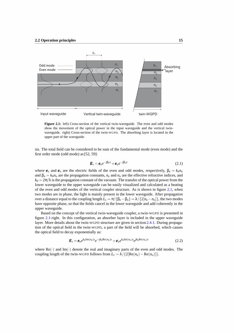
Figure 2.1: left) Cross-section of the vertical twin-waveguide. The even and odd modesshow the movement of the optical power in the input waveguide and the vertical twin-waveguide. right) Cross-section of the twin-WGPD. The absorbing layer is located in theupper part of the waveguide.
sis. The total field can be considered to be sum of the fundamental mode (even mode) and thefirst order mode (odd mode) as [52, 59]:
EEEt = eeeee−jβez+eeeoe−jβoz (2.1)
whereeeee andeeeo are the electric fields of the even and odd modes, respectively,βe = k0ne
andβo = k0no are the propagation constants,ne andno are the effective refractive indices, andk0 = 2π/λ is the propagation constant of the vacuum. The transfer of the optical power from thelower waveguide to the upper waveguide can be easily visualized and calculated as a beatingof the even and odd modes of the vertical coupler structure. As is shown in figure2.1, whentwo modes are in phase, the light is mainly present in the lower waveguide. After propagationover a distance equal to the coupling lengthLc = π/βe−βo= λ/2[ne−no], the two modeshave opposite phase, so that the fields cancel in the lower waveguide and add coherently in theupper waveguide.
Based on the concept of the vertical twin-waveguide coupler, a twin-WGPD is presented infigure 2.1-right. In this configuration, an absorber layer is included in the upper waveguidelayer. More details about the twin-WGPD structure are given in section2.4.1. During propaga-tion of the optical field in the twin-WGPD, a part of the field will be absorbed, which causesthe optical field to decay exponentially as:
EEEt = eeeeek0Im(ne)ze−jk0Re(ne)z+eeeoek0Im(no)zejk0Re(no)z (2.2)
where Re(·) and Im(·) denote the real and imaginary parts of the even and odd modes. Thecoupling length of the twin-WGPD follows fromLc = λ/2[Re(ne)−Re(no)].

16 2. Twin-waveguide pin-photodetector
2.3 Optical and electrical properties ofInGaAs(P)/InP materials
In this section, the basic optical and electrical properties of the InGaAs(P)/InP materials used inthe twin-WGPD structure are described. The properties of the In1−xGaxAsyP1−y materials canbe approximated using Vegard’s law. The properties of the quaternary material such as latticeconstant, bandgap energy, electron and hole masses can be interpolated from the properties ofthe binary compounds GaAs, GaP, InAs, and InP as:
B(x,y) = xyBGaAs+x(1−y)BGaP+(1−x)BInAs +(1−x)(1−y)BInP (2.3)
whereB can be replaced by the lattice constant, energy bandgap, electron or hole mass.In the quaternary material In1−xGaxAsyP1−y lattice matched to InP, the composition frac-
tionsx andy are related by the following expression:
x =0.1896y
0.4176−0.0125y(2.4)
which gives the composition of(x,y) = (0,0) for InP and(0.468,1) for In0.53Ga0.47As.The bandgap energy and wavelength (λg = 1.2399/Eg(eV)) at 300K are related toy by:
Eg(eV) = 1.347−0.778y+0.149y2 (2.5)
The real and imaginary part of the refractive index,nr andni , of the undoped InGaAs(P)materials are expressed as [60, 61]:
nr = (12.35+1.62y−0.055y2)0.5 (2.6)
ni =λα4π
(2.7)
whereα denotes to the optical absorption of the InGaAs(P) materials. Free carriers in a semi-conductor reduce the refractive index ofnr. The refractive index reduction4n is proportionalto the electron concentrationN and the free space wavelengthλ according to:
4n =−Nλ2e2
8π2ε0c2nrme
wheree is the electron charge,c is the velocity of light andme is the effective mass.The electrical permittivity is the square of the refractive index[62]:
ε = εr + jεi = (nr + jni)2 (2.8)
Several basic optical and electrical properties of the InGaAs(P) material used in this chapter atλ=1.55µm wavelength are summarized in table2.1.In0.72Ga0.28As0.61P0.39 material, which has a bandgap wavelength of 1.3µm at room tempera-ture, is denoted as Q(1.3).
2.4 Optical and electrical design of the twin-WGPD 17
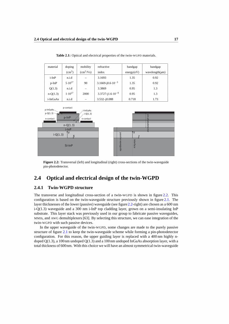
Table 2.1: Optical and electrical properties of the twin-WGPD materials.
material doping mobility refractive bandgap bandgap
(cm3) (cm2/Vs) index energy(eV) wavelength(µm)
i-InP n.i.d – 3.1693 1.35 0.92
p-InP 5·1017 90 3.1669-j0.6·10−3 1.35 0.92
Q(1.3) n.i.d – 3.3869 0.95 1.3
n-Q(1.3) 1·1017 2000 3.3727-j1.6·10−9 0.95 1.3
i-InGaAs n.i.d – 3.532–j0.088 0.718 1.73
i - Q ( 1 . 3 )
n - Q ( 1 . 3 )
S I - I n P
p - Q ( 1 . 3 )p - I n G a A s
p - c o n t a c t
n - c o n t a c tn - c o n t a c t
i - I n P
p - I n Pi - Q ( 1 . 3 )
i - I n G a A s
Xy p a s s i v e w a v e g u i d e
p i n - p h o t o d e t e c t o r
I n t e r f a c e
zy
Figure 2.2: Transversal (left) and longitudinal (right) cross-sections of the twin-waveguidepin-photodetector.
2.4 Optical and electrical design of the twin-WGPD
2.4.1 Twin-WGPD structure
The transverse and longitudinal cross-section of a twin-WGPD is shown in figure2.2. Thisconfiguration is based on the twin-waveguide structure previously shown in figure2.1. Thelayer thicknesses of the lower (passive) waveguide (see figure2.2-right) are chosen as a 600 nmi-Q(1.3) waveguide and a 300 nm i-InP top cladding layer, grown on a semi-insulating InPsubstrate. This layer stack was previously used in our group to fabricate passive waveguides,MMI s, andAWG demultiplexers [63]. By selecting this structure, we can ease integration of thetwin-WGPD with such passive devices.
In the upper waveguide of the twin-WGPD, some changes are made to the purely passivestructure of figure2.1 to keep the twin-waveguide scheme while forming a pin-photodetectorconfiguration. For this reason, the upper guiding layer is replaced with a 400 nm highly n-doped Q(1.3), a 100nm undoped Q(1.3) and a 100nm undoped InGaAs absorption layer, with atotal thickness of 600nm. With this choice we will have an almost symmetrical twin-waveguide

18 2. Twin-waveguide pin-photodetector
structure. In addition, the top cladding layer is a p-doped InP layer to form a pin-junction.The thickness of each layer in the pin-configuration is optimized in section2.4.3 to reach aquantum-efficiency of more than 90%.
The highly-doped n-Q(1.3) layer with a doping level of 1·1019/cm3 acts as an n-contactlayer and as the upper waveguide layer. A non-intentionally doped Q(1.3) layer is used on topof the highly n-doped Q(1.3) layer to match the index of the top guiding layer to the lowerguiding layer and also to make depletion region wider. The p-doped InP top cladding layerhas a charge concentration of 5·1017/cm3 that makes a low resistance path for carriers andkeeps the optical loss in the top cladding layer sufficiently low. The thickness of the p-InPtop cladding layer has to be sufficiently large to keep the optical field tail away from the metalcontact layers. As the photodetector length is short the optical attenuation of the doped layersis negligible with respect to the absorption of the i-InGaAs layer, and a cladding thickness of400 nm for the top p-InP cladding is sufficient to keep the absorption losses of the metal wellbelow the absorption in the detection layer.
On top of the pin-configuration, a highly p-doped Q(1.3) layer and a highly p-doped In-GaAs contact layer are utilized. The highly p-doped Q(1.3) layer plays two important roles:First, the p-Q(1.3) material has a bandgap wavelength between the p-InP and p-InGaAs materi-als (see table2.1), therefore it can prevent charge trapping between the p-InGaAs contact layerand the p-InP top cladding layer. Second, it has a doping concentration between the highly p-doped InGaAs contact layer and the low-doped p-InP cladding layer to form a graded-dopingprofile to prevent further optical loss in the cladding. Moreover, it decreases the path resistanceof the current from the depletion region toward the p-electrode. The dopant concentration ofthe InGaAs contact layer should be high to create a very low contact resistance. Experimentsshow that a 50 nm thick InGaAs contact layer with a doping concentration of 1.5 ·1019/cm3
is sufficient for a very low contact resistance of 2· 10−6Ωcm2 with a metalization layer ofTi/Au (75/200 nm) [64]. The contacts have been designed in aGSG-configuration for theradio-frequency (RF) coupling of the device.
2.4.2 Optical design
Based on electromagnetic theory, the electric and magnetic fields in the forward propagationdirection can be expressed as:
E,HE,HE,H(x,y,z) = ∑m
cmeeem,hhhm(x,y)e−jγmz (2.9)
γm = βm+ jαm (2.10)
whereEEE andHHH denote the electric and magnetic fields as a function of the(x,y,z) position,respectively,eee andhhh are the solutions of the Helmholtz’s equation in the transverse planex0yrespectively,m denotes the mode number,cm denotes the modal amplitude,γm is the modalpropagation constant,βm is the phase propagation constant, andαm is the attenuation constantfor themth mode. It can be shown that for a sufficiently wide twin-WGPDstructure indicated infigure2.2, the expressions foreeem andhhhm can be written as the product of a lateral and transversefield-distribution:

2.4 Optical and electrical design of the twin-WGPD 19
eeem,hhhm(x,y) = eeem,hhhm(x) · eeem,hhhm(y) (2.11)
Therefore, expression2.9 can be determined in thex0y andy0z planes separately. Thus, theelectric and magnetic fields in they0z plane can be written as:
E,HE,HE,H(y,z) = ∑m
cmeeem,hhhm(y)e−jγmz (2.12)
Determination of the electric and magnetic fields in a twin-WGPD is difficult because oneof the layers in the detector is strongly absorbing. In this chapter, a numerically stable modesolver based on a scattering matrix formalism is used [65]. With this mode solver we deter-mine the coupled modal propagation constants and the corresponding fields, both for the inputwaveguide and for the photodetector. At the junction between the input waveguide and the pho-todetector structure, the complex excitation coefficientcm of themth mode in the photodetectoris determined by calculating the overlap integral between the modal fields in the waveguideand the photodetectors as:
cm = 0.5∑n
bn
Zy(eeed
m×hhhwn +eeew
n ×hhhdm) · zdy (2.13)
wherem andn denote the mode numbers,w andd denote the waveguide and the twin-WGPD, andbn denotes the modal amplitude in the input passive waveguide atz = 0. In thespecial case that only the fundamental mode propagates in the input passive waveguide, wehaven = 0 and relation2.13can be simplified as:
cm = 0.5b0
Zy(eeed
m×hhhw0 +eeew
0 ×eeedm) · zdy (2.14)
The optical power of each mode in the planar structure is given by the magnitude of thetime-averaged Poynting vector as:
Sm =12
c2mReeeem×hhh*
m · zzz (2.15)
whereSm is the power of themth mode andcm is the modal amplitude. The total optical powercan be calculated by integration ofSm over the transverse cross-section of the structure as:
P(z) = ∑m
ZsSm ds (2.16)
The relation2.15is valid for a structure if the different modes have power-orthogonality. Thishappens ifHHH=H∗H∗H∗ in the structure. However, in a lossy medium, this relation generally is notvalid and relation2.16has to be used.
In figure2.3, the real and imaginary parts of the electric and magnetic fields atz= 0 areshown for a twin-WGPD structure with thicknesses of the n-Q(1.3), i-Q(1.3), i-InGaAs, andp-InP layers of 400, 100, 100, and 400 nm, respectively. We excite the fundamental mode inthe passive input waveguide. As it is clear, only the fundamental and the first order modes

20 2. Twin-waveguide pin-photodetector
propagate through the twin-WGPD. The real parts of the fields show that the structure is asym-metric, which is caused by the presence of the higher refractive index of the InGaAs layer andthe high-doped Q(1.3) top guiding layer with respect to the non-doped lower guiding layer,in spite of the equal thickness of the top and lower guiding layers. The imaginary part of thefundamental and first order modes show that they have nearly equal amplitude and are in theopposite phase. This brings one advantage that the total field in the input of the twin-WGPD
at z= 0 is real. So, the radiation field (defined as mismatch between the waveguide field andthe twin-WGPDfields) is real. In this specific structure, the power orthogonality exists betweenthe sum of all guided modes and the radiating field. Calculations show the coupling loss tothe radiation field (difference between the optical power in the interface of the input passivewaveguide and the twin-WGPD) is about 0.025 dB that is negligible.
The absorbed optical power in a lossy slab can be determined by [61]:
P = κ0(ε0
µ0)0.5
ZV
nrni |E|2dsdz (2.17)
whereV denotes the absorbing material volume andκ0 denotes the propagation constant inthe free space. The current density generated by the absorbed optical power in the i-InGaAsabsorption layer at position(y,z) can be derived from2.17using the definition for the respon-sivity as:
j(y,z) =ηλe∆Phc∆V
=ηe2π
hc(
ε0
µ0)0.5nrni |E|2 (2.18)
whereη is the internal quantum efficiency,e is the electron charge,c is the light speed,∆V isthe differential volume in the absorption layer, andh is Plank’s constant. In the optimizationprocedure described in the next sections, we assume that all incident photons are absorbed andconverted to electron-hole pairs in the twin-WGPD, i.e.η = 1. The total generated photocurrentfor a lengthl and absorption layer thickness ofd of the twin-WGPD can be determined byintegrating of the current density through the twin-WGPD as
I =Z l
0
Z d
0j(y,z)dydz (2.19)
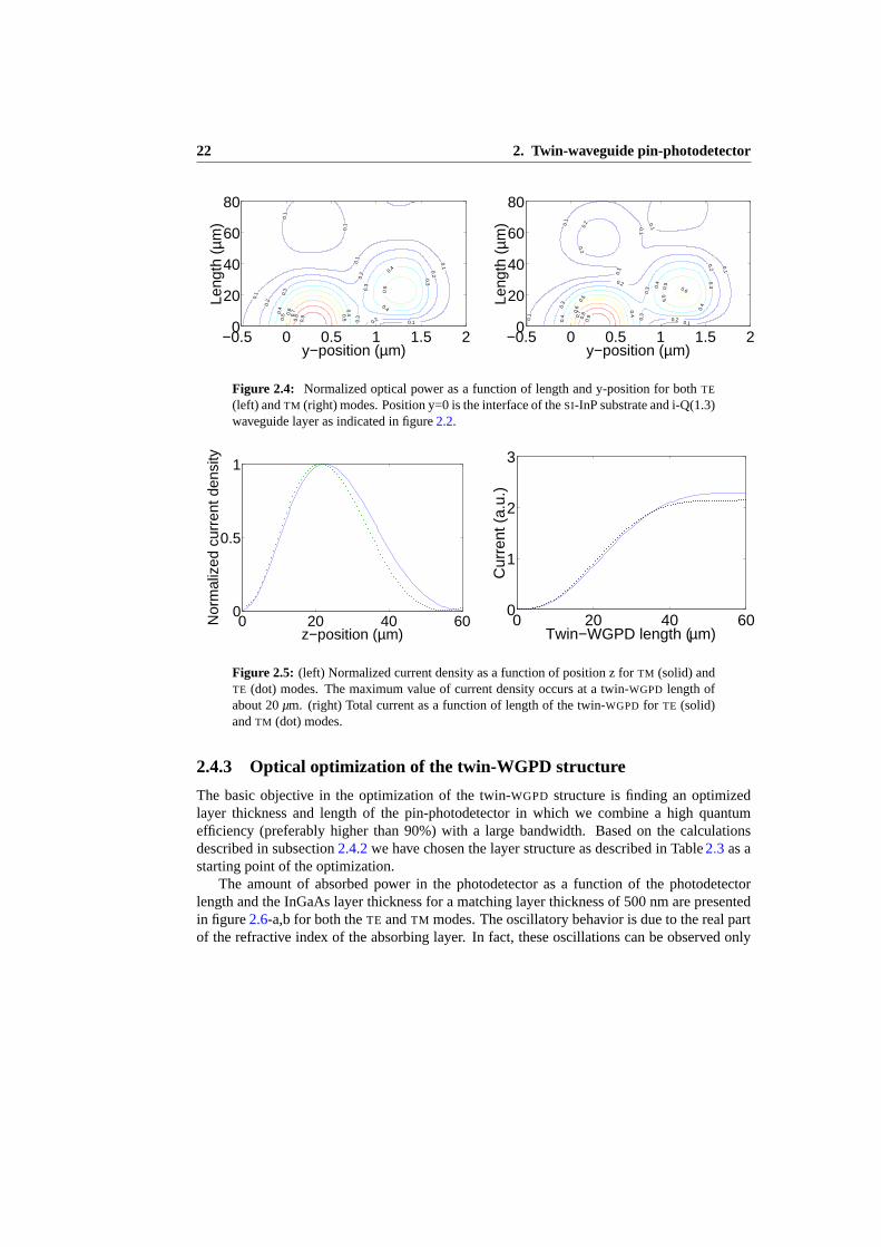
Based on this solution and equations2.15, 2.16, 2.17, and2.18 the optical power distri-bution and current density of the twin-WGPD are determined and shown in figures2.4 and2.5-left. Figure2.4shows that the maximum power in the lower waveguide occurs at the posi-tions z=0µm and z=60µm and in the upper waveguide (twin-WGPD) at the positions z=20µmand z=80µm.∗
Figure2.5-right shows the generated photocurrent versus the twin-WGPD length for bothTE andTM modes that is determined from relation2.19for different lengths and an absorptionlayer thickness ofd = 100 nm. Since there is no absorption in the beginning of the twin-WGPD,no photocurrent is generated there.
∗Effective refractive indices of TE0 and TE1 are 3.3146 and 3.2716, respectively.

2.4 Optical and electrical design of the twin-WGPD 21
−1 0 1 2 3 4
−0.1
−0.05
0
0.05
0.1
y−position (µm)
Ele
ctric
fiel
d (r
eal)
−1 0 1 2 3 4−0.02
−0.015
−0.01
−0.005
0
0.005
0.01
0.015
0.02
y−position (µm)
Ele
ctric
fiel
d (im
ag)
−1 0 1 2 3 4
−0.1
−0.05
0
0.05
0.1
y−position (µm)
Mag
netic
fiel
d (r
eal)
−1 0 1 2 3 4−0.02
−0.015
−0.01
−0.005
0
0.005
0.01
0.015
0.02
y−position (µm)
Mag
netic
fiel
d (im
ag)
Figure 2.3: Electric (upper) and magnetic (lower) fields in the input passive waveguide(“thick solid”) and the twin-WGPD for the fundamental (“-”) and the first order (“-.) modesat positionz= 0. Left-side figures are the real part and right-side figures the imaginary partof the electric and magnetic fields.
22 2. Twin-waveguide pin-photodetector
−0.5 0 0.5 1 1.5 20
20
40
60
80
y−position (µm)
Leng
th (
µm)
0.1
0.1
0.1
0.1
0.1
0.1
0.1
0.2
0.2
0.2
0.2
0.3
0.3
0.3
0.3
0.4 0.4
0.4
0.4
0.5 0.5
0.5
0.6
0.7
0.8
0.9
−0.5 0 0.5 1 1.5 20
20
40
60
80
y−position (µm)
Leng
th (
µm)
0.1
0.1
0.1
0.1
0.1
0.1
0.1
0.2
0.2
0.2
0.2
0.2
0.3
0.3
0.3
0.3
0.4
0.4
0.4
0.4
0.5
0.5
0.5
0.6
0.6
0.7
0.8
0.9
Figure 2.4: Normalized optical power as a function of length and y-position for bothTE
(left) andTM (right) modes. Position y=0 is the interface of theSI-InP substrate and i-Q(1.3)waveguide layer as indicated in figure2.2.
0 20 40 600
0.5
1
z−position (µm)
Nor
mal
ized
cur
rent
den
sity
0 20 40 600
1
2
3
Twin−WGPD length (µm)
Cur
rent
(a.
u.)
Figure 2.5: (left) Normalized current density as a function of position z forTM (solid) andTE (dot) modes. The maximum value of current density occurs at a twin-WGPD length ofabout 20µm. (right) Total current as a function of length of the twin-WGPD for TE (solid)andTM (dot) modes.
2.4.3 Optical optimization of the twin-WGPD structure
The basic objective in the optimization of the twin-WGPD structure is finding an optimizedlayer thickness and length of the pin-photodetector in which we combine a high quantumefficiency (preferably higher than 90%) with a large bandwidth. Based on the calculationsdescribed in subsection2.4.2we have chosen the layer structure as described in Table2.3 as astarting point of the optimization.
The amount of absorbed power in the photodetector as a function of the photodetectorlength and the InGaAs layer thickness for a matching layer thickness of 500 nm are presentedin figure2.6-a,b for both theTE andTM modes. The oscillatory behavior is due to the real partof the refractive index of the absorbing layer. In fact, these oscillations can be observed only

2.4 Optical and electrical design of the twin-WGPD 23
with an absorbing layer which has a real index higher than the real index of the i-Q(1.3) filmlayer [56]. It can be seen that the optimum absorbing layer thicknesses are 100 and 120 nm forTE andTM modes, respectively.
The n-Q(1.3) layer has two roles in the photodetector structure: firstly, it acts as the coreof a waveguide layer for the upper waveguide that is matched to the lower waveguide in orderto enhance the coupling efficiency from the lower passive waveguide to the upper photode-tector structure. Secondly, it acts as a (highly n-doped) contact layer for the detector pin-configuration. The matching-layer is proposed for the first time by Deriet al. [56]. Theyachieved a higher quantum efficiency and a shorter length by adding this layer to their evanes-cently coupledWGPD structure. In this way they changed their evanescently coupled wave-guide detector into a synchronously coupled detector. In figure2.6-c,d, the absorbed opticalpower versus length and matching layer thickness forTE andTM modes are presented. It isseen that for a 500 nm matching layer thickness, the highest absorption and, correspondingly,the smallest detector length is achieved.
The thickness of the p-InP cladding layer has to be sufficient to avoid excessive absorptionof the tails of the optical field in the p-InGaAs contact and metalization layers. The absorbedoptical power as a function of the length and thickness of p-InP layer for bothTE and TM
modes is shown in figure2.6-e,f. It can be seen that for a photodetector with a length of 60µm,a p-InP layer with a thickness of more than 300 nm is required to absorb more than 90% of theoptical power in the detector layer.
The effect of changing the thickness of the n-Q(1.3) layer on the i-InGaAs absorption layerthickness and the length of the twin-WGPD is shown in figure2.7. It shows that with a reductionof the n-Q(1.3) layer thickness from 400nm to 200nm, we have to increase the of the i-InGaAslayer with about 50 nm thickness to reach a 90% quantum efficiency. Whereas, the length ofthe twin-WGPD will be reduced with about 10µm.
In conclusion, a twin-WGPD with a n-Q(1.3) layer thickness of 400 nm, an i-Q(1.3) layerof 100 nm, an i-InGaAs layer of 100 nm, and a p-InP layer of about 400 nm with a length ofabout 60µm is required to absorb an optical power of more than 90%.
2.4.4 Electrical design
The electrical design of the twin-WGPD concerns the design of a structure with a maximumRF-bandwidth. The bandwidth limitations of the twin-WGPD are carrier transit time, parasiticelements, and charge trapping in the hetero-junctions.
Drift transit time
The electron-hole pairs generated by the absorption of photons in the depletion region aremoved to the p- and n-doped layers with a time delay determined by their drift velocity. Kato[66] determined the transit time bandwidth of the waveguide photodetector as:
ftr ∼=3.5v
2πddep(2.20)

24 2. Twin-waveguide pin-photodetector
100 200 300 400
20
40
60
80
100
i−InGaAs layer thickness (nm)
Leng
th (
µm)
10
1010 10
20
2020
20 20
20
30
30
30
30
40
40
40
40 40
5050
50
50
50
50
60
60
60
60
60 60
70
70
70
7080
80
80
80
90
90
90
100 200 300 400
20
40
60
80
100
i−InGaAs layer thickness (nm)
Leng
th (
µm)
1010 10
20 20 2030
3030
40
4040
40 40
50
50
50
50 50
60
60
60
60
60
70
70
70
70
70
70
80
80
80
80
90
90
90
90
(a) (b)
200 400 600 800
20
40
60
80
100
n−Q(1.3) layer thickness (nm)
Leng
th (
µm)
2020
20
40
40
40
40
60
60 60
60
60
80
80
80
80
200 400 600 800
20
40
60
80
100
n−Q(1.3) layer thickness (nm)
Leng
th (
µm)
20 20
20
40
40
40
40
60
60
60
60
60
80
80
80
80
(c) (d)
200 400 600 800
20
40
60
80
100
p−InP layer thickness (nm)
Leng
th (
µm)
10 10 1020 20 20
30 30 3040 40 40
50 50 5060 60 60
70
70 70 70
80
80 80 80
90
90 90 90
200 400 600 800
20
40
60
80
100
p−InP layer thickness (nm)
Leng
th (
µm)
10 10 1020 20 203030 304040 40
50
5050 50
60
6060 60
70
7070 70
80
80
8080 80
90
90
90
90
(e) (f)
Figure 2.6: Coupling efficiency of the pin-photodetector layers forTE (left) andTM (right)polarised modes as a function layer thickness and detector length. Results are shown forvariation of three layers: the detector layer (a and b), the Q1.3 matching layer (c and d) andthe p-doped cladding layer (e and f). In the optimization procedure for each layer, the layerthickness of other layers was kept constant at the value described in section2.4.2.

2.4 Optical and electrical design of the twin-WGPD 25
0 100 200 3000
50
100
i−InGaAs layer thickness (nm)
Leng
th (
µm)
Figure 2.7: 90% optical power absorption contours for three different n-Q(1.3) layer thick-nesses (“*” for 400 nm, “♦” for 300 nm, and “+” for 200 nm) vs. detector length andi-InGaAs layer thickness.
whereddep is the depletion region thickness and ¯v is defined as:
1v4 =
12
(1v4
e+
1
v4h
)(2.21)
whereve andvh are electron and hole velocity in the depletion region that are given by [67]:
ve =µeE +βvsat,eEγ
1+βEγ (2.22)
vh = vsat,h tanh
(µhEvsat,h
)(2.23)
whereE is the electric field through the depletion region and the parameters of expressions2.22and2.23for InGaAs material are listed in table2.2. Based on these values the velocities of theelectron and holes are plotted in figure2.8. It is noticed that for an electric field higher than20 KV/cm, the electrons and holes reach their saturation velocities.
The depletion layer thickness can be determined from expression:
ddep=[
2ε0εr(Vbi−V)eNd
]1/2
(2.24)
whereVbi is the build-in voltage,V is the applied reverse bias voltage, andNd is the impurityconcentration in the depletion region. For a depletion region withNd = 3 ·10+16 /cm3 , Vbi '0.5 V andεr = 13, a depletion layer thickness of about 150 nm at a reverse bias voltage of 0 Vis found, which is in agreement with our experiments results. This value gives a transit timebandwidth of about 50 GHz.

26 2. Twin-waveguide pin-photodetector
Table 2.2: Electrical parameters of the InGaAs material for equations2.22and2.23.
description value
electron mobility (cm2/Vs) 10500
hole mobility(cm2/Vs) 420
electron saturation velocity (cm/s) 5.4·106
hole saturation velocity (cm/s) 4.8·106
β 7.4·10−10
γ 2.5
0 10 20 30 40 500
1
2
3x 10⁷
Electric field (KV/cm)
Vel
ocity
(cm
/s)
Figure 2.8: Carrier velocities vs. electric field for InGaAs material (“dot” for holes and“solid” for electrons).
RC-elements
The RC-elements of the twin-WGPD are shown in figure2.9. The separation of charges in thedepletion region is equivalent to a parallel plate capacitor. The equivalent junction capacitanceis given by
Cpd =ε0εrAddep
(2.25)
whereA is the area of the capacitor plates corresponding to the area of the depletion region,ddep is the thickness of the depletion region,ε0 is the vacuum permittivity andεr is the relativepermittivity of the intrinsic InGaAs layer. The ohmic resistance of the n-Q(1.3), p-InP bulkmaterial and contact layers can be determined from
Rp =dp
eµhNpA(2.26)

2.4 Optical and electrical design of the twin-WGPD 27
i - Q ( 1 . 3 )
n - Q ( 1 . 3 )
S I - I n P
p - Q ( 1 . 3 )p - I n G a A s
p - c o n t a c t
n - c o n t a c t
i - I n P
p - I n P i - Q ( 1 . 3 )i - I n G a A s
i
Figure 2.9: Physical interpretation of theRC-elements of the twin-WGPD. In this figure,wc =6 µm, dp= 360 nm,ddep=200 nm,dn=320 nm, andwn= 8 µm.
Rn =wn
eµeNndnl(2.27)
Rs =ρc
wcl(2.28)
wheredp is thickness of the p-InP layer,Np is its doping level,µh is its hole mobility,wn isthe distance from the middle of the mesa to the n-contact,µe is the electron mobility in then-Q(1.3) layer,Nn is its doping level anddn its thickness ,l is the length of the photodetector,ρc is the specific contact resistance of the p-InGaAs layer, andwc is the width of the contactopening on the p-mesa. The dark resistanceRd indicates the current leakage of the twin-WGPD
at the reverse bias voltage and without illumination.An approximation for theRC-limited bandwidth that only takes into account the junction
capacitance and the series resistances is given by [66]
fRC =1
2πRCpd(2.29)
whereR is the summation of the series resistances includingRp, Rn/2, Rs andRL=50Ω. Thevalues ofwn, dp, wc, anddn are indicated in figure2.9. Based on these values and a twin-WGPD
length of 60µm a junction capacitanceCpd=106 fF and a resistanceR=56Ω are predicted.

28 2. Twin-waveguide pin-photodetector
E c
E v e l e c t r o n h o l e
i-InGa
Asi-Q
(1.3)
n-InPp-InP
p-Q(1.
3)p-I
nGaA
s
h f
Figure 2.10: Schematic view of the pin-photodetector structure in the twin-WGPD (top) andenergy-band diagram under the reversed bias voltage (down). Charge trapping is illustratedin notches.
Charge-trapping in hetero-junctions
As shown in table2.1, the bandgap energy of the p-InP layer and the p-InGaAs contact layerare 0.72 and 1.73 eV, respectively. When electron-hole pairs that are generated in the deple-tion region, travel towards the contact layers, they can be trapped in the barriers of the doublehetero-structures [68]. Charge trapping causes recombination of electron and holes in het-erostructure junctions and decreases the speed of carriers traveling toward electrodes. For thisreason, a p-Q(1.3) layer with an energy bandgap of 1.3 eV is placed between p-InGaAs andp-InP layers to reduce the effects of the barrier (see figure2.10). We used the simulation resultsobtained by Steenbergen [64] to determine the barrier height.

2.4 Optical and electrical design of the twin-WGPD 29
0 50 100 1500
20
40
60
Length (µm)
Ban
dwid
th (
GH
z)
0 5 10 15 200
20
40
60
Width (µm)
Ban
dwid
th (
GH
z)
Figure 2.11: (left)- Bandwidth vs. length of the twin-WGPD with a width of 8µm. (right)-Bandwidth vs. width of the twin-WGPD with a length of 60µm. In both figures, “*” , “.”,and “solid” refer toftr, fRC, and ft, respectively.
Diffusion transit time
The diffusion transit time is defined as the time that it takes for the carriers generated outsidethe depletion region to diffuse to that region. In the twin-WGPD, the depletion layer is boundedby layers with a wider bandgap. If the intrinsic region is fully depleted, and if the bandgapof the layers adjacent to the absorption layer is lower than energy of the incident photons, allof the incident photons will be absorbed in the depletion region and no carriers are generatedoutside the depletion layer. As a result, no bandwidth reduction due to diffusion effects willoccur [69].
Twin-WGPD bandwidth
If we assume that the limiting factors for the bandwidth are independent of each other, the3-dB bandwidth of the twin-WGPD can be approximated as [66, 70]
1
f 2t
=1
f 2tr
+1
f 2RC
(2.30)
where ft is the 3-dB electrical bandwidth andftr and fRC are defined in relations2.20and2.29,respectively. In figure2.11, the bandwidth of a twin-WGPD as a function of length and widthand the other parameters as indicated in figure2.19, is presented. It can be seen that the twin-WGPD with the length and width of 60 and 8µm, respectively, has a bandwidth about 25 GHz.Figure2.11-left also shows that for a too short twin-WGPD, ftr is dominant.

30 2. Twin-waveguide pin-photodetector
Table 2.3: Layer stack with specifications of the twin-WGPD and passive waveguide.
layer material doping level function thickness
# (cm−3) (nm)
1 InGaAs 1.5·1019 p-contact 60
2 InGaAsP(1.3) 8·1017 p-doped 50
3 InP 5·1017 p-doped 410
4 InGaAs intrinsic absorption 100
5 InGaAsP(1.3) intrinsic index match 100
6 InP intrinsic stop etch 10
7 InGaAsP(1.3) 1·1019 n-contact 390
8 InP intrinsic cladding 190
9 InGaAsP(1.3) intrinsic stop etch 10
10 InP intrinsic cladding 100
11 InGaAsP(1.3) intrinsic guiding 600
12 InP intrinsic substrate 500
13 SI-InP SI – –
2.5 Fabrication of the twin-WGPD
2.5.1 Epitaxial growth
The twin-guide layer stacks were grown with Low-Pressure Metal Organic Vapor Phase Epi-taxy (LP-MOVPE). In this technique, the carrier gases are injected in a relatively low-vacuumchamber, typically less than 76 mTorr, and at anRF-heating temperature of 625C. For theInGaAsP/InP based materials, the vapor sources are usually AsH3, PH3, In(CH3)3, Ga(CH3)3,and Zn(CH3)3 for the dopant [64, 71]. The specification of the fabricated wafer including layerthickness and dopant profile is shown in table2.3.
2.5.2 Processing scheme
In order to process the photodetector, a number of 5 different masks have been used. A maskfor the definition of the p-mesa (mask #1), a mask to define the p- and n-contacts (mask #2),a mask for the definition of the passive waveguides (mask #3), a mask for the definition ofthe contact opening in the SiN passivation layer† (mask #4), and a mask for the definition ofthe metal pattern (mask #5). In the following steps, the fabrication of the twin-WGPD with thepassive waveguides is briefly described.
†In this thesis, SiN is equal to SiNx

2.5 Fabrication of the twin-WGPD 31
1. Orientation: The orientation of the photodetectors has to be in the direction [011]. Theused evaporation machine at TU Delft could not cover the metal on the side walls witha side wall angle of 90 or more. Therefore, a wet chemical etch for the definition ofp-mesa and n-region was utilized to create side walls with slopes less than 90 degrees.
2. Definition of the p-mesa:At first, a 100 nm SiN was deposited on the wafer by PlasmaEnhanced Chemical vapor Deposition (PECVD). This layer served as a mask for thep-mesa etching. Then a layer ofHPR-504 photoresist is spun onto the wafer. The p-mesa pattern was defined on the photoresist using the mask #1 and after lithography, thepattern was transferred to the SiN-layer with aBHF etching solution (see figure2.12-a).
3. RIE-etch of the p-mesa:H2:CH4 dry RIE-etching is used to etch the p-InGaAs/Q(1.3)top layers (see fig2.12-b) away everywhere except at the contact regions.
4. Selective wet chemical etching of the detector mesa:Etching the p-InP protectionlayer with the solution HCL:H3PO4 (1:4), etching the InGaAs absorption layer with thesolution H2SO4:H2O2:H2O (1:1:10), and etching the InP stop layer with the solutionHCL:H3PO4 (1:4) (see fig2.12-c).
5. SiN deposition: Removal of the SiN on top of the p-mesa and then redeposition of100 nm SiN on the wafer (see fig2.12-d).
6. Definition of the n-contact: The second mask is used to remove the SiN everywhereexcept in the p- and n-contact regions. Then the highly n-doped Q(1.3) layer is wet-chemically etched (see fig2.12-e).
7. Definition of the passive waveguide:Removing SiN on the n- and p-contact region witha BHF solution and then redeposition of 100 nm SiN to define the passive waveguides.Subsequently, mask #3 is used to define the passive waveguide pattern on the SiN-layerfollowed byRIE-etching of the (shallow) waveguides.
8. Opening contact:Using mask #4, the n- and p- contacts are opened by chemical etchingof the SiN-layer (see fig2.12-f).
9. Metalization: The metalization pattern was defined using mask #5 and a negative pho-toresist. Ti/Au (70/200 nm) is evaporated on the chip by an evaporation machine at alow temperature . Finally, the processing is followed by a lift-off (see figure2.12-g).
In figure2.13, a SEM photograph of the realized device is shown. The p-contact metalizationin the middle and two n-contact metalizations in both sides of the p-mesa can be seen in thetwin-WGPD part. It also shows the input optical passive waveguide and the output electricalprobe-pad.

32 2. Twin-waveguide pin-photodetector
S I - I n Pi - Q ( 1 . 3 )i - I n Pn + - Q ( 1 . 3 )p + - I n P
S i Ni - Q ( 1 . 3 )i - I n G a A s p + - I n G a A s
p - - Q ( 1 . 3 )
(a) (b)
(c) (d)
(e) (f)
(g)
Figure 2.12: Fabrication scheme of the twin-WGPD.

2.6 Optical and electrical measurements 33
I n p u t p a s s i v e w a v e g u i d e
T w i n - W G P D
G r o u n d
G r o u n d
S i g n a l
P r o b e - p a d
Figure 2.13: SEM photograph of the twin-WGPD.
2.6 Optical and electrical measurements
To determine the electro-optical behavior of the twin-WGPD, a number of twin-WGPDs withlengths of 30, 40, 50, 60, and 70µm have been measured. The measurements are classi-fied as static and high-frequency measurements. In the static measurements, the responsivity,quantum efficiency, dark current, and capacitance are measured. The frequency-response ofthe twin-WGPDs is determined in three ways: using an optical-heterodyning technique, witha 20 GHz lightwave component analyzer, and by measuring the output reflection coefficientof the photodetectors with a 40 GHz network analyzer. Meanwhile, the parameters of anequivalent-circuit small-signal model of the device have been extracted from the output reflec-tion coefficient measurements [57].
2.6.1 Static characterization
Quantum efficiency and responsivity
The quantum efficiency and responsivity of the twin-WGPDs are measured by coupling theoptical beam from a tunable laser source to theAR-coated facet of the input passive waveguide

34 2. Twin-waveguide pin-photodetector
30 40 50 60 700
0.5
1
Length (µm)
Qua
ntum
effi
cien
cy
−25 −20 −15 −1010
−1
100
101
102
Pho
tocu
rren
t (µA
)
Optical power (dBm)
Figure 2.14: left) Internal (“♦”) and external (“*”) quantum efficiency as a function of thedetector length at –5 V bias voltage. right) Measured photocurrent vs. input optical powerfor various lengths of the photodetector: 30µm (“”), 40µm (“©”), 60µm (“♦”), and 70µm(“?”).
via a tapered lensed fiber. The measured internal and external quantum efficiency for varioustwin-WGPDs at−5 volts bias voltage and a wavelength of 1530 nm are shown in figure2.14-left. The internal quantum efficiency is calculated by measuring the twin-WGPD responsivityand considering an estimated 4.5 dB coupling and connector loss. It demonstrates that morethan 90% of the optical power is absorbed by a photodetector with a 60µm length, coincidingwith the device simulations. The responsivity of the photodetectors can be determined about0.4 A/W for a 60µm long device.
The measured photocurrent at –5Volts biased voltage and 1530 nm wavelength is presentedin figure2.14-right. It can be seen that behavior of the photodetector is linear respect to inputoptical power.
Capacitance and dark current
The capacitance as a function of the applied bias voltage is measured with a multi-frequencyLCR-meter at different frequencies in a dark environment and with anAC-signal amplitude of100 mV. In figure2.15-left, the measured capacitance versus bias voltage for a 60µm longdevice at 1 kHz frequency is shown. For a reverse-bias voltage larger than 5 Volts, the pho-todetector is fully depleted. The capacitance is also measured for different lengths of the pho-todetector and the results are depicted in figure2.15-right. The measured capacitance includesboth the photodetector and parasitic capacitances of the probe-pad.
The I -V characteristics of the photodetectors were measured for several photodetectors. Adark current of less than 10 nA at−5 Volts was observed.

2.6 Optical and electrical measurements 35
−10 −8 −6 −4 −2 00.5
1
1.5
2
2.5
Bias voltage (V)
Cap
acita
nce
(pF
)
0 20 40 60 800.7
0.75
0.8
0.85
0.9
0.95
1
Length (µm)
Cap
acita
nce
(pF
)
Figure 2.15: left) Capacitance vs. voltage measured for a 60µm long twin-WGPD at afrequency of 1 kHz with 100 mVAC-signal amplitude. right) Capacitance vs. twin-WGPD
length measured at−5 V bias voltage, with 1 MHz frequency and 100 mVAC-signal am-plitude.
2.6.2 High-frequency response
Heterodyning technique
In order to determine the frequency response of the twin-WGPD, an optical heterodyning tech-nique is used [72–74]. This technique is based on the mixing of twoCW laser beams withdifferent wavelengths in a directional coupler. The beating of the optical fields creates a signalmodulated with a frequency equal to the frequency difference of the lasers.
In figure 2.16, a schematic view of the heterodyne measurement setup is shown. One ofthe tunable lasers generates an optical signal at a fixed wavelengthλ1 and the wavelength ofthe second tunable laser is tuned atλ2 = λ1 +4λ. The two generated optical fields are mixedin a 50% coupler. One of the coupler outputs is connected to a wavelength meter to measure
the frequency difference of the two tunable lasers asfRF = c(
1λ1− 1
λ2
). The other output of
the coupler is connected to anEDFA to boost the optical power. A lensed fiber-tip is used tocouple the light into the input waveguide of the twin-WGPD.
If we assume that the optical fields of the signals generated by the tunable lasers have adifference polarization angle ofφ, the optical power that reaches the twin-WGPD is:
P(t) = 0.5(P1 +P2 +2
√P1P2 cosφ cos(ωt)
)(2.31)
whereω1 = c/λ1, ω2 = c/λ2, ω = ω1−ω2, andc is the velocity of light. The photocurrentgenerated by the photodetector due to this optical power is given by:
ip(t) = I1 + I2 +2√
I1I2 H(ω) cosφ cosωt (2.32)
whereH(ω) is the frequency response of the twin-WGPD, I1 = ℜP1 andI2 = ℜP2 andℜ is theresponsivity of the photodetector.

36 2. Twin-waveguide pin-photodetector
A HF-probe transfers the generated electrical current,ip(t) to a 40GHz digital oscilloscopevia a bias-tee andHF-coaxial cables. The measured voltage by the digital oscilloscope can beexpressed as:
Vp(t) = Z0(I1 + I2 +2
√I1I2 Hm(ω) cosφ cosωt
)= Vp,dc+Vp,ac (2.33)
whereZ0 = 50 Ω is the input impedance of the digital oscilloscope,Vp,dc = Z0(I1 + I2) is DC-part,Vp,ac = 2Z0
√I1I2Hm(ω) cosφ cos(ωt) is theAC-part of output voltage, andHm(ω) is the
measured frequency response. The frequency response of the twin-WGPD from the measuredAC-part ofVp(t) can be determined as:
Hm(ω) =Vp,ac
2Z0√
I1I2 cosφcos(ωt)(2.34)
If the polarization angle between the optical signals is constant,φ= constant, thenHm(ω) isproportional with the measuredAC-voltage.
To measure the frequency response of the twin-WGPD, one of the tunable lasers is fixed at awavelength of 1550 nm and the beat frequency of the generatedRF-signal is tuned by varyingthe wavelength of the other tunable laser.
The measured frequency response includes the frequency response of the digital oscillo-scope,RF-coaxial cables,RF-connectors, bias tee, andRF-probe. For this reason, it is requiredto de-embed the measured frequency response of the twin-WGPD. The transmission of all com-ponents is frequency-dependent , the frequency response of the twin-WGPD can be determinedby [75]:
H(ω) = Hm(ω)γp (2.35)
whereHm(ω) is the measured frequency response,γp is the response of the probe, biastee,RF-cables and digital oscilloscope. To findγp, a photodetector with a known frequencyresponse is utilized.
The frequency response of the twin-WGPD with a detector length of 60µm and a widthof 8 µm is shown in figure2.17, in both before and after de-embedding. The presence of theripples is due to a standing wave between the probe-tip and the twin-WGPD.
Lightwave component analyzer
A direct method to characterize the frequency response of a twin-WGPD is by using a lightwavecomponent analyzer. A Lightwave component analyzer, HP8703A, with a frequency range of20 GHz has been utilized to determine the frequency response of the twin-WGPDs. The mea-sured frequency response of the 60µm long device is shown in figure2.18. The measurementresult reveals a bandwidth of more than 20 GHz, a ripple with a resonance frequency of 2 GHz,and an increasing mismatch with rising frequency. This ripple is due to the impedance mis-match between the probe and the twin-WGPD. One major drawback of this measurement isthe restriction to 20 GHz due to the maximum frequency of the instrument. However, becauseof the internal calibration of the instrument, this is a straightforward method to measure thefrequency response of the twin-WGPD.

2.6 Optical and electrical measurements 37
T L 1
T L 2
E D F A D U Tp r o b b i a s - T
d i g i t a lo s c .
W a v e l e n g t h m e t e r O p t i c a l f i b e r
R F - c a b l e
5 0 % c o u p l e r
Figure 2.16: Measurement setup that is used for measuring the frequency response of thetwin-WGPD with the heterodyning technique.
- 8
- 6
- 4
- 2
00 1 0 2 0 3 0
F r e q u e n c y ( G H z )
Relat
ive re
spon
se (d
B)
( b )
( a )
Figure 2.17: Relative frequency response of a twin-WGPD with 60 µm length and 8µmwidth, that is measured with a heterodyning setup. (a) Before de-embedding and (b) afterde-embedding.

38 2. Twin-waveguide pin-photodetector
0 5 10 15 20−6
−5
−4
−3
−2
−1
0
Frequency (GHz)
Nor
mal
ized
freq
uenc
y re
spon
se (
dB)
Figure 2.18: Relative frequency response of a twin-WGPD with 60 µm length and 8µmwidth, that is measured with a 20 GHz lightwave component analyzer.
2.6.3 Small-signal equivalent-circuit model
For the design and development of a receiver, an accurate and efficient model of the twin-WGPD
is required. The modeling of the twin-WGPD allows us to understand the complex phenomenaof the optical and microwave interaction. In addition, an accurate model of the photodetectorcan help in the design of a transimpedance-preamplifier. This goal can be achieved by per-forming an output reflection-coefficient measurement and fitting the parameters of a suitablemodel to the measured data using an dedicated software [76]. The relation between outputreflection coefficientΓ and output impedanceZ(ω) is given by:
Z = Z01+Γ1−Γ
(2.36)
whereZ0 = 50Ω is the characteristic impedance of the measurement system.

2.6 Optical and electrical measurements 39
Figure 2.19: The small-signal equivalent circuit of a twin-WGPD including the probe-padelements.
f r e q ( 5 0 . 0 0 M H z t o 4 0 . 0 5 G H z )
S(1,1
)ce
ll2_te
ststru
cture_
2..S(2,2
)
f r e q ( 5 0 . 0 0 M H z t o 4 0 . 0 5 G H z )
test_s
tructu
re_da
mage
d_6..
S(2,2
)tes
t_stru
cture_
dama
ged_
7..S(2,2
)tes
t_stru
cture_
dama
ged_
8..S(2,2
)tes
t_stru
cture_
dama
ged_
9..S(2,2
)tes
t_stru
cture_
dama
ged_
10..S
(2,2)
7 0 m m6 0 m m
5 0 m m
3 0 m m4 0 m m
Figure 2.20: (left) Measured and fitted output reflection coefficient vs. frequency for atwin-WGPD with 60 µm length shown on a Smith chart (measurement “solid” and fittedmodel ”5”). (right) Measured output reflection vs. frequency for the twin-WGPD withvarious lengths.
In order to extract the equivalent-circuit model of the twin-WGPD, an on-wafer networkanalyzer measurement was performed in a range of 50 MHz to 40 GHz without illuminationof the photodetector. Figure2.19shows an equivalent-circuit model of the twin-WGPD. In thismodel,Cpd is the junction capacitance of the reverse-biased detector;Rd is the dark currentresistance;Rs is the series resistance;RL is the load resistance; andLs, Csh, andGsh are theequivalent-circuit elements of theCPW transmission line [8, 10].
Figure2.20-left shows the measured and fitted output reflection coefficient of a twin-WGPD
with a length of 60µm and a width of 8µm on a Smith chart. By measuring the output reflec-tion coefficient for several lengths of the twin-WGPDs (see figure2.20-right), the value of thejunction capacitance and the series resistance are determined which is depicted in figure2.21.As we can see, the extracted components are in good agreement with the calculated values. Inthese measurements, the average values of the shunt resistanceRsh=25 KΩ, the series induc-tanceLs=55pH, the dark current resistanceRd=1.5KΩ, and the shunt capacitanceCsh=0.15pFfor various length of devices are extracted.

40 2. Twin-waveguide pin-photodetector
0
4 0
8 0
1 2 0
0 2 0 4 0 6 0 8 0l e n g t h ( m m )
Capa
citan
ce (fF
)
0
5
1 0
1 5
Resis
tance
()
Figure 2.21: Junction capacitance and series resistance of the twin-WGPD extracted fromoutput reflection coefficient measurements. Solid lines are simulated values for series resis-tance and junction capacitance.
2.7 Conclusion
The structure of the twin-WGPD is based on a vertical twin-waveguide scheme in which twomodes (even and odd) propagate through the guiding layers. Several twin-WGPDs with lengthsvarying between 30 and 70µm (with 10µm steps) and 8µm width were fabricated. The mea-sured internal quantum efficiency for the different lengths of the photodetector demonstratesthat more than 90% of the optical power is absorbed in a 60µm long twin-WGPD, whichmatches with device simulations.
To measure the frequency response of the twin-WGPDs, three approaches are used: a het-erodyning technique, extraction of an equivalent-circuit model of the twin-WGPDs by measur-ing the output reflection coefficient, and using a lightwave component analyzer. The hetero-dyning technique shows a 25 GHz bandwidth for a 60µm long twin-WGPD which is in goodagreement with the bandwidth that follows from the extracted model (see figure2.22). Themeasurements with a 20 GHz lightwave component analyzer also illustrate that the bandwidthis greater than 20 GHz. This comes close to the best results reported for twin-guide WGPDs:a bandwidth of 25 GHz [37, 58].

2.7 Conclusion 41
- 1 0
- 8
- 6
- 4
- 2
0
0 5 1 0 1 5 2 0 2 5 3 0F r e q u e n c y ( G H z )
Relat
ive re
spon
se (d
B)
Figure 2.22: Frequency response of a 60µm long and 8µm wide twin-WGPD that is mea-sured by two methods: heterodyning (solid) and output reflection coefficient technique(dot).

42 2. Twin-waveguide pin-photodetector

Chapter 3
Hybrid integration of a MWR andTI-TWA
In this chapter, the design and realization of a hybrid integrated WDM receiver, includinga monolithic integrated eight-channel, high-speed and polarization independent optical re-ceiver (comprising an AWG demultiplexer and eight photodetectors) and a trans-impedancetraveling-wave amplifiers are described. Before the components were hybridly integrated, sev-eral optical and electrical measurements were carried out to characterize the optical multi-wavelength receiver, electrical amplifiers and bondings. The optical and electrical chips werethen mounted on a submount, ribbon-bonded and characterized. The hybrid integrated re-ceiver shows a bandwidth of over 18 GHz for each of the measured channels.
3.1 Introduction
The realization of aWDM receiver requires the combination of several components such as ademultiplexer, photodetectors and front-end amplifiers. In figure3.1, a schematic configurationof the MWR is presented. An optical signal with eight modulated wavelengthsλ1, λ2,..., λ8
enters anAWG demultiplexer where the wavelengths are spatially separated and each signal isrouted to one of the eight photodetectors. In each photodetector, the modulated optical signal isconverted into an electrical current signal and subsequently, in the front-end trans-impedancetraveling amplifier (TI-TWA), the input current is converted to an output voltage for furtherprocessing. Electronic signal processing stages can process the voltage signal to extract theinformation.
Monolithic integration of all components in InP-based materials has been a great challengefor researchers for more than one decade. An early example of an integratedWDM receiver
43
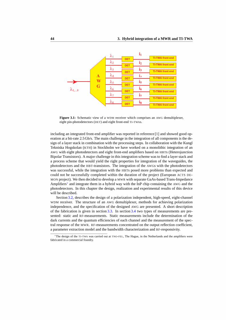
44 3. Hybrid integration of a MWR and TI-TWA
i 2 i 3 i 4 i 5 i 6 i 7 i 8
i 1
T I - T W A f r o n t e n d D E T D E T D E T D E T D E T D E T D E T D E T
AWG l 1 , . . . 8
T I - T W A f r o n t e n d
T I - T W A f r o n t e n d T I - T W A f r o n t e n d T I - T W A f r o n t e n d T I - T W A f r o n t e n d T I - T W A f r o n t e n d T I - T W A f r o n t e n d
l 1 l 2 l 3 l 4 l 5 l 6 l 7 l 8
Figure 3.1: Schematic view of aWDM receiver which comprises anAWG demultiplexer,eight pin-photodetectors (DET) and eight front-endTI-TWAs.
including an integrated front-end amplifier was reported in reference [1] and showed good op-eration at a bit-rate 2.5Gb/s. The main challenge in the integration of all components is the de-sign of a layer stack in combination with the processing steps. In collaboration with the KunglTekniska Hogskolan (KTH) in Stockholm we have worked on a monolithic integration of anAWG with eight photodetectors and eight front-end amplifiers based onHBTs (HeterojunctionBipolar Transistors). A major challenge in this integration scheme was to find a layer stack anda process scheme that would yield the right properties for integration of the waveguides, thephotodetectors and theHBT-transistors. The integration of theAWGs with the photodetectorswas successful, while the integration with theHBTs posed more problems than expected andcould not be successfully completed within the duration of the project (EuropeanACTS DE-MON project). We then decided to develop aMWR with separate GaAs-based Trans-ImpedanceAmplifiers∗ and integrate them in a hybrid way with the InP chip containing theAWG and thephotodetectors. In this chapter the design, realization and experimental results of this devicewill be described.
Section3.2, describes the design of a polarization independent, high-speed, eight-channelWDM receiver. The structure of anAWG demultiplexer, methods for achieving polarizationindependence, and the specification of the designedAWG are presented. A short descriptionof the fabrication is given in section3.3. In section3.4 two types of measurements are pre-sented: static andRF-measurements. Static measurements include the determination of thedark currents and the quantum efficiencies of each channel and the measurement of the spec-tral response of theMWR. RF-measurements concentrated on the output reflection coefficient,a parameter extraction model and the bandwidth characterization andRF-responsivity.
∗The design of theTI-TWA was carried out atTNO-FEL, The Hague, in the Netherlands and the amplifiers werefabricated in a commercial foundry.

3.2 Design of a polarization independent MWR 45
Figure 3.2: Schematic view of theAWG.
In sections3.5, the design and characterization of GaAs-based front-endTI-TWA for a40 Gb/s receiver are presented. The measurement results include theS-parameters and noisefigure (NF). In section3.6, several simulation and measurement results for wire bondings andribbon bondings are presented and then compared. They show that ribbon bonding has a lowertransmission attenuation and lower reflection compared to wire bonding. In section3.7 themeasurement results of the hybrid integrated receiver are presented.
3.2 Design of a polarization independent MWR
3.2.1 Basic AWG-operation principle and design parameters
The basic operation of theAWG is explained by using figure depicted in figure3.2. It consistsof two de/focusing slab regions (or free propagation regions) which are connected by an arrayof waveguides with a constant length difference4L. The light enters from the input waveguideinto a slab region, the free propagation region (FPR), in which the optical field diverges and iscoupled into the array arms. After traveling through the array waveguides, the light beam nowconverges on a focal point in the end of the secondFPR, where it is coupled into the outputwaveguide. The path-length difference in the array arms results in an equal phase delay in eachwaveguide which changes with wavelength. This causes a tilt of the phase front in the outputFPRand a changing of the location of the focal point as a function of wavelength.
For a signal which enters the first slab region under an angleϕ and the second slab regionunder an angleφ, we can derive theAWG equation based on diffraction theory as [77]:
Ns(λ)dasinϕ+Ng(λ)4λ+Ns(λ)dasinφ = mλ (3.1)
whereNs andNg are the effective indices in the slab region and waveguide, respectively,da isthe separation of the array waveguides at the slab-array interface, andm is the grating diffrac-tion order, which is determined by choosing4L , and represented as:
m=Ng(λc)4L
λc(3.2)

46 3. Hybrid integration of a MWR and TI-TWA
whereλc is the central wavelength for whichϕ = φ = 0.In a practical design of anAWG, the number of channels, the central wavelength, and the
channel spacing are some of the input parameters for the design . The waveguide spacing ofthe array waveguides at theFSRshould be chosen as small as the lithographic resolution allowsin order to minimize the coupling losses between the slab and the waveguide array. However,irregular filling of the gap between those waveguides introduces variations in the phase transferof the array which increases the crosstalk. So in a practical design, the spacing gaps are chosensomewhat larger than the lithographic resolution. The focal length is determined from themaximum acceptable excess loss for the outer wavelength channels, or from the required freespectral range, which is the spacing between adjacent diffraction orders.
In table3.1, a list of the design parameters of theAWG that we used is summarized. TheAWG demultiplexer has eight channels with a channel spacing of 400GHz (3.23 nm) and a freespectral range of 38.47 nm, operating around a central wavelength of 1556 nm. The width ofthe normal waveguides is 3µm and in the polarization compensation region (see section3.2.3)they are 1.5µm wide. This is the smallest width that still avoids excessive phase errors due toprocess deviations and also yields an acceptable propagation loss. The lateral transition from3µm to 1.5µm is done adiabatically with a 50µm linear taper. A minimum radius of curvatureof 500µm is chosen to have a low radiation loss in the curved parts of theAWG.
3.2.2 Polarization dispersion compensation methods
A polarization independentAWG is used for mostWDM communication networks, where thepolarization at the receiver is undefined. The polarization dependency of theAWG originatesfrom the polarization dependency of waveguides in theAWG which is a result of the differencein index contrast in the transverse and lateral directions.
There are different ways to compensate the birefringence of anAWG reported in refer-ence [63]: inserting a compensating waveguide section in each of the arms of theAWG, usingnon-birefringence waveguides, using a half-wave plate in the arms of theAWG, and using anAWG with a special design to overlap the imaging ofTE andTM polarization for two differentdiffraction orders. Below, the advantages and disadvantages of each method are explained.
The square waveguide (figure3.3-a) is a straightforward way for obtaining a polarizationindependent waveguide. However, this method requires a square waveguide embedded in anisotropic material [78]. A small deviation of the dimension of the core, will bring polarizationdependence. The raised-strip waveguide (figure3.3-b) with a proper width and waveguidelayer thickness ratio makes it an option also for high-contrast waveguides that can be used incompactAWGs.
In the half-wave plate method (figure3.3-c), a half-wavelength plate is inserted in the mid-dle of theAWG. The inputTM mode is converted to theTE mode and theTE input modeconverts into theTM mode. This method is applicable to waveguides with a small numeri-cal aperture (NA) in which the light can travel across the half-wavelength distance with smalldiffraction losses. In InP-based waveguides with largeNA, this method is not applicable. Themethod was first applied in silica-based [79] and LiNbO3 [80] AWGs.

3.2 Design of a polarization independent MWR 47
Table 3.1: Design parameters of the polarization independentAWG demultiplexer
Parameter Value
InP cladding layer thickness 300 nm
Q(1.3) waveguide layer thickness 600 nm
Etch depth 400 nm
Width of normal waveguides 3µm
Width of the compensated section 1.5µm
Etch depth of the compensated section 200 nm
Minimum gap between array waveguides at fan-out500 nm
Minimum gap between input/output waveguides 2.4µm
Minimum bending radius 500µm
Number of array waveguides 59
Length of the free propagation region 581.15µm
Array acceptance factor 4
Compensation length increment 18.286µm
Central wavelength 1.556µm
Channel spacing 3.229 nm
Free spectral range 38.472 nm
TE-TM shift before birefringence correction 5.45 nm
Array order (m) 35
If the free spectral range (FSR) of the AWG is chosen equal to the polarization dispersion,ordermof theTE polarized mode will be matched to orderm−1 of theTM mode, (figure3.3-d[81]. The main disadvantage of this method is that all wavelength channels should fit withinthe FSRdesigned for the polarization dispersion whereas for the waveguide which we use thepolarization dispersion is usually in the order of 4 nm. This is too small to support theFSR
required for our application (8×3.2 nm).The polarization dispersion of anAWG can be compensated by replacing a part of the wave-
guide in the array arms with a compensating waveguide that has a different birefringence. Thismethod was applied to a silica-basedAWG for the first time by Takahashi [82] and for the firsttime to an InP-basedAWG by Zirngibl [30]. This method requires accurate information aboutthe refractive indices of the materials, the waveguide geometry, and a good fabrication process.A small deviation in the waveguide width and the layer thickness can bring a noticeable shiftin the polarization dispersion [64]. This method was used in our design, and will be discussedin more detail in the next section.

48 3. Hybrid integration of a MWR and TI-TWA
I n G a A s P
I n P
W
W
I n P
I n G a A s P D
W
(a) (b)
h a l f - w a v e p l a t e
a r r a y a r m
T E m - 1T M m - 1
T E m
T M m
(c) (d)
Figure 3.3: Schematic view of the (a) buried waveguide with an equal width and thicknessW (b) raised strip waveguide with a thicknessD and a widthW (c) using a half-wave platein the arms of theAWG (d) matchingTE andTM modes.
3.2.3 Array arm birefringence compensation
Among the various way of the polarization dispersion compensation methods, the method ofreplacing of a part of the array arms with a compensating waveguide that has a different bire-fringence is chosen (see figure3.7). In order to increase the birefringence in the compensatingwaveguide, and hence reduce the required length, we reduce the InP top-cladding layer thick-ness. Figure3.4 shows that the birefringence strongly increases when the InP cladding layerthickness is reduced from 300 nm (for a normal waveguide) to 100 nm (for a dispersion com-pensated waveguide).
In a non-compensatedAWG, the length difference of theAWG arms at the central wave-lengthλc is given by
∆L =mλc
N(λc)(3.3)

3.2 Design of a polarization independent MWR 49
0 0.5 10.005
0.01
0.015
0.02
0.025
InP cladding layer thickness (µm)
Bire
frin
genc
e
Figure 3.4: Calculated birefringence as a function of the InP cladding layer thickness for awaveguide width of 1.5µm at 1.55µm wavelength.
in which N(λc) is the effective index at central wavelengthλc andm is the order of theAWG demultiplexer. The different effective index forTE and TM modes creates a shift atcentral wavelength equal to
∆λpol = λTENTE,λTE−NTM,λTE
NTE,λTE−λTE∂NTM
∂λ |λTE
(3.4)
in which NTE,λTE, NTM,λTE , λTE andλTM are the modal effective indices and center wave-lengths for theTE andTM polarizations, respectively.
In the polarization dispersion compensatedAWG, an increment length ofδL with a differ-ent birefringence is inserted between two adjacent waveguides in the array arm. The phasedifference,∆ϕ, at the output of arms due to the different arm lengths of the array arm,δL and∆L, for TE andTM modes are:
∆ϕTE = κ0(∆LNTE +δL(NTE−nTE)) (3.5)
∆ϕTM = κ0(∆LNTM +δL(NTM −nTM)) (3.6)
in which N andn are the effective refractive indices in the normal and the compensated wave-guide structure, respectively. In the polarization independent structure, we have∆ϕTE=∆ϕTM ,from which a relation for the incremental lengthδL follows as
δL = ∆L∆N
∆n−∆N(3.7)
where∆N = NTE−NTM and∆n = nTE−nTM are the waveguide birefringence in the normaland compensated waveguide structures, respectively.

50 3. Hybrid integration of a MWR and TI-TWA
L i
L i + D L = L i + D L
L n
W i t h o u t p o l a r i s a t i o n d i s p e r s i o n c o m p e n s a t i o n
L i
L i + 1 = L i + D L
L n
W i t h p o l a r i s a t i o n d i s p e r s i o n c o m p e n s a t i o n
l n
l i
l i + 1 = l i - d l
Figure 3.5: Array arms before inserting a different waveguide for the polarization disper-sion compensation (left) and after (right).
A large birefringence can be achieved by completely removing the top cladding layer [48],but this results in high coupling loss between the two waveguide structures. For this reasonwe chose a wide, shallowly etched waveguide with a thick InP top cladding layer in the ar-ray waveguides and removed only a part of the cladding layer in the compensation sections,which resulted in a low-loss polarization-independentAWG demultiplexer. In figure3.5, theconfiguration of the array arms before and after inserting the compensation section is shown.
In practice, a mask for the triangle part is designed and fabricated after the chip has beencharacterized. This is feasible for research purposes, but not for industrial fabrication. So, thebirefringence is experimentally determined from the wavelength shift between theTE andTM
response of theAWG and the shape of the triangle is then designed to compensate birefringence.In figure3.6, a measured spectral response of the multi-wavelength receiver before etching ofthe polarization-dispersion compensating triangle is shown. The shift of central wavelengthfor TE andTM polarizations is about 5.45nm, which is about 1nm different from the simulatedvalue. The spurious peaks in the spectrum are due to various optical paths that existed betweenoutput and the input of theAWG before cleaving into single cells. The insertion loss of theAWG is about 4.5 and 5.5 dB forTE andTM polarized light, respectively.
3.2.4 Photodetector design
The structure and the optical and electrical behavior of the photodetector based on the twin-guide scheme are explained in chapter2. The photodetector structure is placed on top of thewaveguide layers. The specifications of the layer stacks in the photodetector structure are

3.2 Design of a polarization independent MWR 51
1520 1530 1540 1550 1560−40
−30
−20
−10
0
Wavelength (nm)
Opt
ical
res
pons
e (d
B)
Figure 3.6: Spectral response of theAWG before etching of the polarization compensationtriangle forTE (solid) andTM (dot) polarized light.
presented in table2.3. The width and length of the twin-WGPD are chosen 8µm and 60µm, re-spectively, which results in a quantum efficiency of more than 90% and a frequency bandwidthof about 40 GHz (without considering the parasitic elements of the probe-pad).
The p- and n-contacts are arranged in a ground-signal-ground (GSG) configuration to easeon-wafer measurements (see more details in figure2.13). The p-contact is located on top ofthe p-mesa with a width of 6µm which is sufficient to allow for a possible misalignment of themask during lithography (the misalignment of lithography is maximum 1µm). The n-contactelectrodes on top of the n-doped layer are placed on both sides of p-mesa. The separationgaps between p- and n-contacts are 4.5µm and the width of ground electrode is 21µm. Theprobe-pad is situated on the semi-insulating InP with signal and ground widths of 50µm andseparations of 50µm (the pitch of signal and ground electrodes is 100µm). The length ofthe probe-pad is 230µm which can be reduced by 50% for the next designs to decrease theparasitic elements. The probe-pad and photodetector electrodes are connected by an angled-taper transition with a length of more than 100µm. The photodetectors are placed on both sidesof the receiver-chip, spaced by 900µm, which reduces the electrical crosstalk between thechannels (see figure2.13). In this circuit layout, in order to save space, each optical waveguideis placed at a 90 angle with respect to theRF-probe-pad. Since the pads are relatively small,

52 3. Hybrid integration of a MWR and TI-TWA
Figure 3.7: Photograph of aMWR. TheAWG demultiplexer is in the middle and the eightphotodetectors are in the upper and lower sides of chip. Two photodetectors on the right-hand side are the photodetectors for calibration of the device. The polarization-dispersioncompensating triangle is visible in the middle of theAWG arms.
the additionalRF-loss this might induce is negligible. The pads end at the edge of the chip, sothat the bond wire connections to the pre-amplifier can be kept short.
The optical access waveguide entering the photodetector is tapered with an adiabatic taperwith a length of 100µm from a width of 3µm to an output width of 10µm. This wide waveguideminimizes the light divergence under the detector mesa, where it is no longer laterally confined.On each of the four corners of p-mesa an additional 3×3µm2 square is positioned, to preventthe etching of the p-mesa corners by the chemical as indicated in figure3.8-right.
3.3 Fabrication
The fabrication process of the eight-channelMWR is identical to that used for the twin-WGPD
which is described in section2.5. A photograph of the realized device and twoSEM photosare shown in figures3.7and3.8. In figure3.7, the realized device including theAWG (with thetriangle part in the middle of array arms) and the eight photodetectors on both sides of the chipis shown. The good quality of the fabrication processing for both theAWG and the p-mesa ofthe photodetector can be seen in figure3.8.
An additional fabrication step was used for etching the polarization dispersion compen-sation triangle. In this chemical-etch step, which is performed directly after the metalizationevaporation and lift-off, the wafer is locally etched to partly remove the InP top cladding layer.This is done using HCL/H3PO4 in the triangle windows defined by soft-baked photoresist.During etching, gas forms that results in an irregular etching and rough surfaces. An etch-stop

3.4 Characterization of the optical multi-wavelength receiver 53
Figure 3.8: SEM photographs of (left) the fan-out section in theAWG and (right) the p-mesaof the photodetector. Both photographs show a good quality of processing.
layer at 200 nm from the waveguide layer in combination with a slight over-etch is used toovercome this problem.
The input facet of the photodetector wasAR-coated with SiO2 , with a thickness optimizedfor a wavelength of 1.55µm. Part of the coating is deposited on top of the chip, and this isvisible as a band on the right part of the chip in figure3.7.
3.4 Characterization of the optical multi-wavelength re-ceiver
In this section, the characterization of the monolithic integratedAWG and eight twin-WGPDs ispresented. The realized device is characterized by static measurements, including dark current,quantum efficiency, andAWG transmission spectral response. Subsequently, theMWR is char-acterized atRF-frequencies by measuring the output reflection coefficient of the photodetectorsandRF-transmission response.
3.4.1 Static characterization
I-V curves
The I-V curves of the eight photodetectors in a dark environment, at room temperature andwithout illumination were measured using a Keithly source-current meter. The dark currentmeasurements at various bias voltages are shown in figure3.9. The leakage current is verysmall, rising from 1nA at−1V to less than 10nA at−4V. The dark current density, calculatedusingJ = I/S, is equal to 2 A/m2 at−1 V and 42 A/m2 at−5 V whereS= 8×60µm2 is thearea where the current flows through the p-mesa.
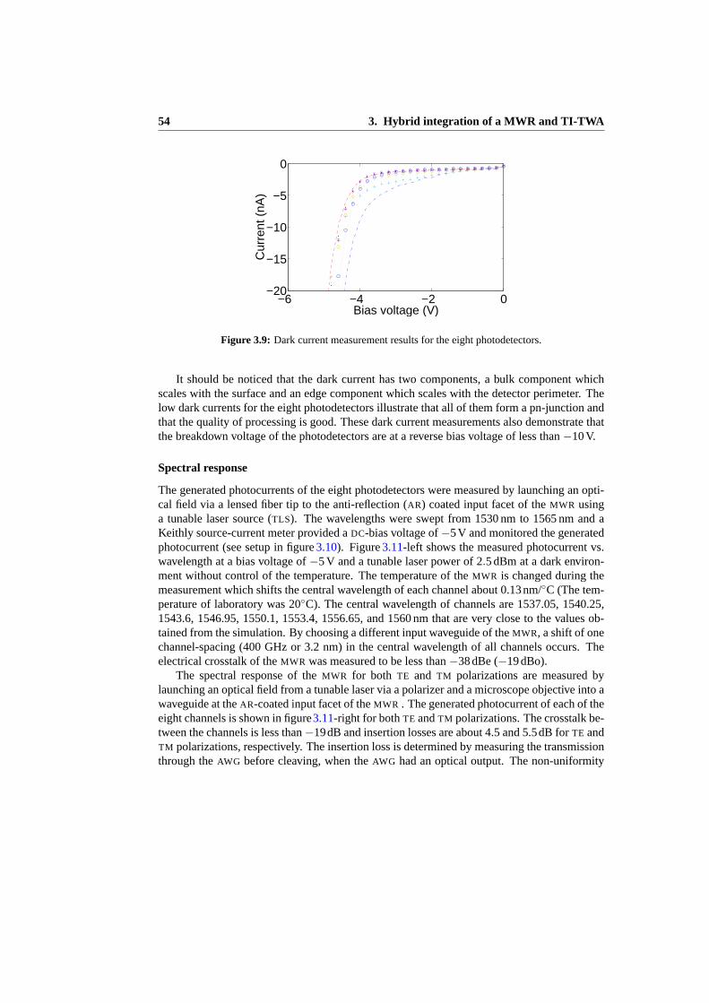
54 3. Hybrid integration of a MWR and TI-TWA
−6 −4 −2 0−20
−15
−10
−5
0
Bias voltage (V)
Cur
rent
(nA
)
Figure 3.9: Dark current measurement results for the eight photodetectors.
It should be noticed that the dark current has two components, a bulk component whichscales with the surface and an edge component which scales with the detector perimeter. Thelow dark currents for the eight photodetectors illustrate that all of them form a pn-junction andthat the quality of processing is good. These dark current measurements also demonstrate thatthe breakdown voltage of the photodetectors are at a reverse bias voltage of less than−10 V.
Spectral response
The generated photocurrents of the eight photodetectors were measured by launching an opti-cal field via a lensed fiber tip to the anti-reflection (AR) coated input facet of theMWR usinga tunable laser source (TLS). The wavelengths were swept from 1530 nm to 1565 nm and aKeithly source-current meter provided aDC-bias voltage of−5V and monitored the generatedphotocurrent (see setup in figure3.10). Figure3.11-left shows the measured photocurrent vs.wavelength at a bias voltage of−5 V and a tunable laser power of 2.5 dBm at a dark environ-ment without control of the temperature. The temperature of theMWR is changed during themeasurement which shifts the central wavelength of each channel about 0.13nm/C (The tem-perature of laboratory was 20C). The central wavelength of channels are 1537.05, 1540.25,1543.6, 1546.95, 1550.1, 1553.4, 1556.65, and 1560 nm that are very close to the values ob-tained from the simulation. By choosing a different input waveguide of theMWR, a shift of onechannel-spacing (400 GHz or 3.2 nm) in the central wavelength of all channels occurs. Theelectrical crosstalk of theMWR was measured to be less than−38 dBe (−19 dBo).
The spectral response of theMWR for both TE and TM polarizations are measured bylaunching an optical field from a tunable laser via a polarizer and a microscope objective into awaveguide at theAR-coated input facet of theMWR . The generated photocurrent of each of theeight channels is shown in figure3.11-right for bothTE andTM polarizations. The crosstalk be-tween the channels is less than−19dB and insertion losses are about 4.5 and 5.5dB forTE andTM polarizations, respectively. The insertion loss is determined by measuring the transmissionthrough theAWG before cleaving, when theAWG had an optical output. The non-uniformity

3.4 Characterization of the optical multi-wavelength receiver 55
T L S K e i t h l y
M W R c h i pO p t i c a l f i b e r
e l e c t r i c a l w i r e sn e e d l e s
Figure 3.10: Measurement setup for static experiments. A computer controls theTLS andthe Keithly source-current meter in which the wavelength and power of theTLS and theoutput voltage of the Keithly are set, and then it records the generated photocurrent via theKeithly.
1530 1535 1540 1545 1550 1555 1560 156510
−3
10−2
10−1
100
Wavelength (nm)
No
rma
lize
d s
pe
ctr
al re
sp
on
se
1520 1530 1540 1550 1560−50
−40
−30
−20
−10
0
Wavelength (nm)
Sp
ectr
al re
sp
on
se
(d
B)
Figure 3.11: (left) The generated photo-current vs. wavelength of theMWR. Light wascoupled into the chip with a lensed fiber. (right) Optical response of theMWR vs. wavelengthfor TE (dot) andTM (solid) polarizations. Light was coupled into the chip with a microscopeobjective and a polarizer.

56 3. Hybrid integration of a MWR and TI-TWA
of the channels is about 1 dB and the residual polarization dispersion is smaller than 1 nm andincreased during the measurement. A part of the dispersion shift comes from a temperature riseduring the characterization of theMWR. The response of the photodetector of channel two isreduced by approximately 15 dB, most likely due to a defect in the optical waveguide leadingto that detector.
Responsivity
The responsivity and efficiency of channels have been determined by measuring the outputpower of theTLS, the output current of the photodetectors and the on-wafer and couplinglosses. To characterize each channel, the output power of the tunable laser vs. wavelengthwas measured before performing each measurement. The spectral power of each channel wasthen recorded to find the central wavelength of each channel. The external responsivity of thephotodetectors is determined for each channel at different bias voltages, see figure3.12. Theinternal and external responsivities and the quantum efficiency of a channel are determinedas follows: theTLS output optical power for e.g. channel three was−3.2 dBm (0.48 mW) atcentral wavelength of 1543.6 nm. The measured current was about 55µA at a bias voltageof −5 V. This corresponds to a responsivity of 0.11 A/W or an 9% external efficiency. Byconsidering 4 dB coupling loss, 0.5 dB connector, polarization control and optical fiber lossesand anAWG insertion loss of 4.5 dB forTE and 5.5 dB forTM (total loss about 9 dB), wedetermine an internal responsivity of about 0.88 A/W for the photodetector of channel three,which is equal to 71% internal quantum efficiency.
The external efficiencies are between 8% and 11.5% at a reverse bias voltage of−5 V forvarious channels. From figure3.12we also see that that the external responsivities of the pho-todetectors are approximately constant from 0 to−7V which indicates that the photodetectorsare fully-depleted.
3.4.2 RF-characterization
Three methods forRF-characterization of theMWR chip were carried out to determine severalparameters of the photodetectors. Each method can present some information about theRF
behavior of the photodetectors and theMWR. From the output reflection coefficient, we candetermine several parameters: the 3-dB bandwidth, the parasitic elements, and the depletionthickness. Characterizing with a lightwave component analyzer is a straight-forward way tomeasure the 3-dB bandwidth of theMWR. Measuring the pulse response of the receiver is away to determine 3-dB bandwidth and to understand the effects of various rise times on thefrequency response. TheBER and eye diagram measurements show the expected behavior ofthe receiver in real optical networks. The main goal for all measurements was finding the 3-dBbandwidth and then to compare the results of these methods.

3.4 Characterization of the optical multi-wavelength receiver 57
−7 −6 −5 −4 −3 −2 −1 00.1
0.11
0.12
0.13
0.14
0.15
0.16
Bias voltage (V)
Ext
erna
l res
pons
ivity
(A
/W)
Figure 3.12: External responsivity as a function of the bias voltage for eight photodetectorsmeasured at the top of the passband of each channel.
Output reflection coefficient measurement
On-wafer output-reflection-coefficient measurements are performed in the frequency range50 MHz to 40 GHz using a network analyzer in a dark environment at different bias voltages.Figure3.13 shows the output reflection coefficient of a photodetector at bias voltages of 0,−2, −5, −7, and−10 Volts. Since the geometrical dimensions of the photodetector are smallcompared to theRF-wavelength, the device can be modeled by an equivalent circuit of lumpedelements, depicted in figure2.19. The parameters of the model are determined through fittingthe measured data to the model. TheS-parameters resulting from the model with the fittedparameters, are denoted asSsimulated. The measured and simulatedS-parameters agree betterthan 0.1% using the error function:
error=N
∑i=1
(Ssimulated,i −Smeasured,i)/Smeasured,i (3.8)
The photodetector elements including photodetector capacitance and series resistance,Cpd
andRs, are bias voltage dependent, which is shown in figure3.14. With increasing the reversebias voltage, the depletion thickness becomes wider and the capacitance of the photodetectorwill decrease from 250 fF at 0 V to 150 fF at−10 V. During the measurements it was observedthat increasing the reverse bias voltage over−10 V no longer changes the output reflectioncoefficient. The depletion thickness, calculated according to relation2.24, as a function of thereverse bias voltage is shown in figure3.15. At bias voltage 0 V, the depletion thickness is ap-proximately equal to thickness of the non-intentionally doped region. The parasitic elementsof the equivalent circuit are also determined by using a commercial optimizer software (Ag-ilent’s Advanced Design System:ADS) as: Lsh' 120 pH,Rsh'20,Csh'150 fF. The value of

58 3. Hybrid integration of a MWR and TI-TWA
f r e q ( 5 0 . 0 0 M H z t o 4 0 . 0 5 G H z )
cell3_p
d3_5
v..S(2,2
)ce
ll3_p
d3_7
v..S(2,2
)S(2,2
)ce
ll3_p
d3_2
v..S(2,2
)
0 V
- 1 0 V
- 2 V- 5 V- 7 V
Figure 3.13: Output reflection coefficient of a photodetector at bias voltages of 0,−2, −5,−7, −10 volts on the Smith chart.
0 5 10150
200
250
300
Cap
acita
nce
(fF
)
Reverse bias voltage (V)0 5 10
10
11
12
13
14
15
Ser
ies
resi
stan
ce (
Ω)
Reverse bias voltage (V)
Figure 3.14: (left) Capacitance of a photodetector vs. bias voltage. (right) Series resistanceof the photodetector vs. bias voltage.
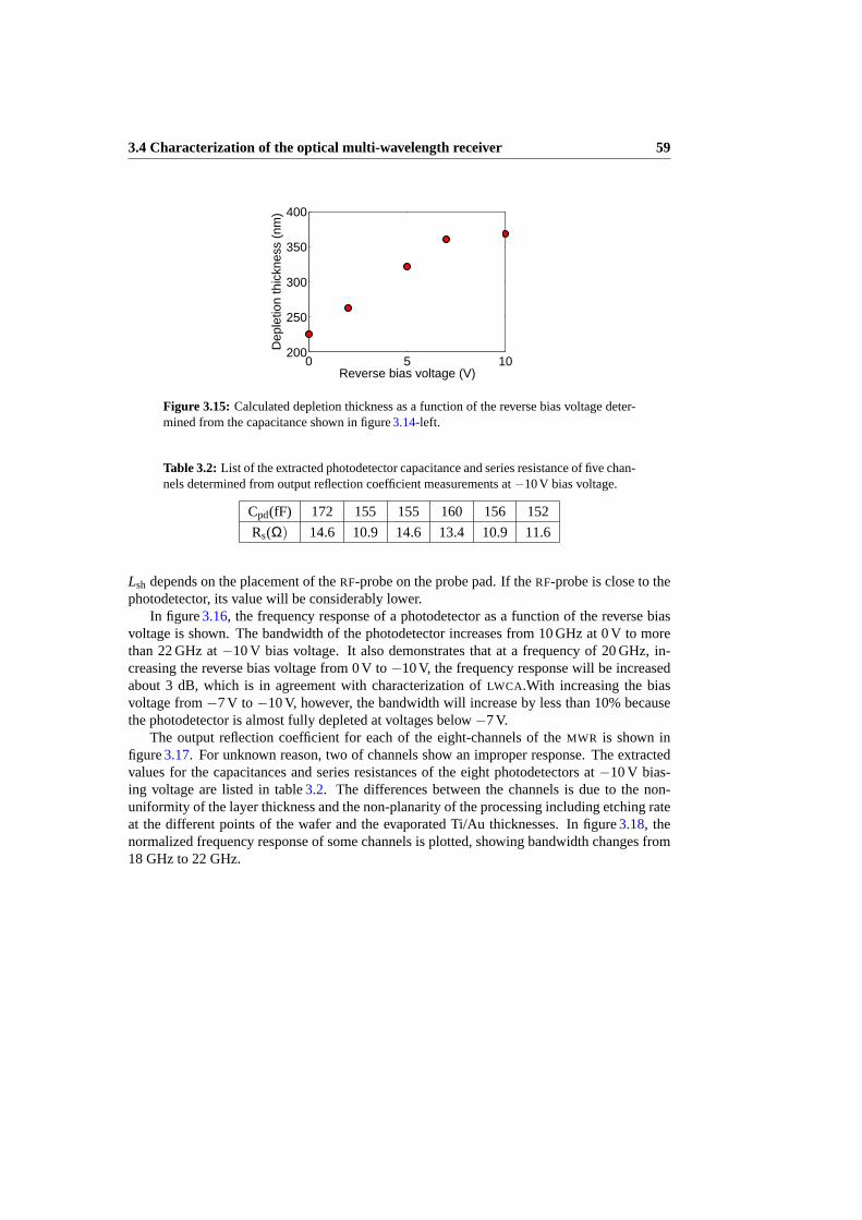
3.4 Characterization of the optical multi-wavelength receiver 59
0 5 10200
250
300
350
400
Dep
letio
n th
ickn
ess
(nm
)
Reverse bias voltage (V)
Figure 3.15: Calculated depletion thickness as a function of the reverse bias voltage deter-mined from the capacitance shown in figure3.14-left.
Table 3.2: List of the extracted photodetector capacitance and series resistance of five chan-nels determined from output reflection coefficient measurements at−10 V bias voltage.
Cpd(fF) 172 155 155 160 156 152
Rs(Ω) 14.6 10.9 14.6 13.4 10.9 11.6
Lsh depends on the placement of theRF-probe on the probe pad. If theRF-probe is close to thephotodetector, its value will be considerably lower.
In figure3.16, the frequency response of a photodetector as a function of the reverse biasvoltage is shown. The bandwidth of the photodetector increases from 10 GHz at 0 V to morethan 22 GHz at−10 V bias voltage. It also demonstrates that at a frequency of 20 GHz, in-creasing the reverse bias voltage from 0 V to−10 V, the frequency response will be increasedabout 3 dB, which is in agreement with characterization ofLWCA.With increasing the biasvoltage from−7 V to−10 V, however, the bandwidth will increase by less than 10% becausethe photodetector is almost fully depleted at voltages below−7 V.
The output reflection coefficient for each of the eight-channels of theMWR is shown infigure3.17. For unknown reason, two of channels show an improper response. The extractedvalues for the capacitances and series resistances of the eight photodetectors at−10 V bias-ing voltage are listed in table3.2. The differences between the channels is due to the non-uniformity of the layer thickness and the non-planarity of the processing including etching rateat the different points of the wafer and the evaporated Ti/Au thicknesses. In figure3.18, thenormalized frequency response of some channels is plotted, showing bandwidth changes from18 GHz to 22 GHz.

60 3. Hybrid integration of a MWR and TI-TWA
0 10 20 30 40−15
−10
−5
0
Frequency (GHz))
Nor
mal
ized
res
pons
e (d
B)
3 dB
12 GHz
0 V−2 V
−5 V−7 V−10 V
Figure 3.16: Normalized frequency response of a photodetector vs. frequency for variousbias voltages of 0,−2,−5,−7, and−10 V. With increasing the reversed bias voltage from0 V to−10 V, the bandwidth of the photodetector increases about 10 GHz.
RF-responsivity
A straightforward way to measure the frequency response of theMWR is using a lightwavecomponent analyzer (LWCA). A lightwave component analyzer can measure a receiver’s trans-fer function as a ratio of theRF-current output from the receiver to the intensity modulatedoptical input power expressed in A/W or in dB as (see figure3.19):
Responsivity(dB)= 20log10ℜ(A/W)1(A/W)
(3.9)
In figure3.20, a setup for measuring the optical/electrical (O/E) response with an externaltunable laser source (TLS) and a lightwave component analyzer is shown. TheLWCA HP8703A
has an internal tunable laser source at wavelength 1300 nm, so we need an external tunablelaser at the desired wavelength for each channel of theMWR. As shown in the figure, forcalibrating the measurement system, we should connect the input and output of the opticaland electrical ports of theLWCA, separately, by an optical and an electrical thru connection.A polarization controller (PC) is used between theTLS and theLWCA to achieve a maximumsignal level. After calibration of theLWCA at the center wavelength of each channel, wecan measure theRF-responsivity of theMWR with sweeping the frequency from 130 MHz to20GHz (see figure3.21). We apply the biasing voltage to the photodetector via a bias tee and aKeithly current-source meter, and monitor theDC-photocurrent generated by the photodetector.

3.4 Characterization of the optical multi-wavelength receiver 61
f r e q ( 5 0 . 0 0 M H z t o 4 0 . 0 5 G H z )
cell3_p
d1_1
0v..S
(2,2)
cell3_p
d2_1
0v..S
(2,2)
cell3_p
d3_1
0v..S
(2,2)
cell3_p
d4_1
0v..S
(2,2)
cell3_p
d5_1
0v..S
(2,2)
cell3_p
d6_1
0v..S
(2,2)
cell3_p
d7_1
0v..S
(2,2)
cell3_p
d8_1
0v..S
(2,2)
Figure 3.17: Output reflection coefficients of the photodetectors of all channels at−10 Vbias voltage. Two channels show a non-perfectRF-behavior.
0 10 20 30 40−10
−8
−6
−4
−2
0
Frequency (GHz))
Nor
mal
ized
res
pons
e (d
B)
Figure 3.18: Normalized frequency response of five channels at−10 V bias voltage. The3-dB bandwidth changes from lowest value 18GHz to maximum value of 22 GHz.

62 3. Hybrid integration of a MWR and TI-TWA
I
P o
d
d
I
P
S l o p e =R e s p o n s i v i t y
Figure 3.19: Definition of theRF-responsivity asℜ= δIδP (A/W).
T L S L W C A
P CR F - c a b l e
O p t i c a l f i b e r s T h r uFigure 3.20: A lightwave component analyzer with an external tunable laser source (oper-ating int the 1550nm wavelength window) with the electrical and optical thru connectors tocalibrate the setup.
The RF-responsivity of a photodetector for bias voltages of 0,−2, −5, −7 and−10 Vis shown in figure3.22. By increasing the bias voltage from 0 V to−10 V, the bandwidthis increased by about 5 dB at 20 GHz which is in good agreement with the result shown infigure3.16. In figure3.23theRF-responsivity of a photodetector is shown forTLS output pow-ers of−1, 0, 3, 5, 8, 10, and 13dBm at−10V bias voltage. It can be seen that with increasingthe optical power, theRF-power is increased by twice the optical power from 0 to 10dBmTLS
powers. For powers of theTLS exceeding 10 dBm, the internal modulator of theLWCA wassaturated. An important note in figures3.22 and3.23 is that in both figures the experimen-tal results are partly not de-embedded for adapters, and bias-tee.If we assume a conservativeRF-loss of about 4 dB (at 20 GHz) for all components, we can find a good agreement betweenthe two methods of extracting parameters from the output reflection coefficient measurementsby fitting the model, and from a direct measurement using the lightwave component analyzerdepicted in figures3.16and3.22. To investigate theRF-coupling from adjacent channels, we

3.5 Design of the trans-impedance traveling-wave amplifier 63
T L S L W C A
M W R c h i p
P CR F - c a b l e
O p t i c a l f i b e r s K e i t h l e y
B i a s - t e e
Figure 3.21: A measurement setup to characterize theMWR chip. A Keithly source-currentmeter is used to apply a bias voltage and to measure theDC-current. The modulated opticalfield from theLWCA enters theMWR chip via a fiber tip and theRF-signal is collected by aRF-probe.
adjusted theTLS wavelength to the adjacent channel wavelength and measured anRF-crosstalkless than−30 dB as is depicted in figure3.24.
3.5 Design of the trans-impedance traveling-wave amplifier
A trans-impedance traveling-wave amplifier (TI-TWA) for amplifying the signal from the inte-gratedMWR has been developed byTNO-FEL. A short description of the design criteria andthe characterization results will be given here.
In the design of theTI-TWA matched with the photodetectors in theMWR, the followingconstraints have to be considered:
• A high-speed front-end amplifier suitable for a 40 Gb/s optical receiver. According torules of thumb, 30 GHz bandwidth is sufficient to support a 40 Gb/s data rate.

64 3. Hybrid integration of a MWR and TI-TWA
0 5 10 15 20−20
−15
−10
−5
0
Frequency (GHz))
Nor
mal
ized
freq
uenc
y re
spon
se (
dB)
−10 V
−7 V −5 V
−2 V
0 V
Figure 3.22: RF-responsivity for bias voltages of 0,−2,−5,−7,−10 V and aTLS poweroutput of +13 dBm at a central wavelength channel of 1546.95 nm, measured with theLWCA.
0 5 10 15 20−40
−30
−20
−10
0
Frequency (GHz))
Nor
mal
ized
res
pons
ivity
(dB
)
−1 dBm
0 dBm
3 dBm
5 dBm
8 dBm
10 dBm13 dBm
Figure 3.23: RF-responsivity for theTLS output powers of−1, 0, 3, 5, 8, 10, and 13 dBmat a bias voltage of−10 V and a wavelength of 1543.6 nm, matching the channel center.

3.5 Design of the trans-impedance traveling-wave amplifier 65
0 5 10 15 20−60
−40
−20
0
Frequency (GHz))
Nor
mal
ized
res
pons
ivity
(dB
)
Figure 3.24: RF-responsivity of a channel and an adjacent channel. The maximumRF-crosstalk is about−30 dB.
M - d e r i v e d s e c t i o n
LL 9
LL 1 0
LL 1 6
CC 3C = 1 . 0 p F
CC 1C = 1 . 0 p FP o r tP 1N u m = 1
LL 1 7
R =L = 1 . 0 n H
LL 1 1LL 8
RR 1R = 5 0 O h m
CC 5C = 1 . 0 p F
LL 2 1
R =L = 1 . 0 n H
LL 1 2J F E T _ N F E T1 LL 1 3J F E T _ N F E TJ F E T 2
J F E T _ N F E TJ F E T 4
LL 1 5
J F E T _ N F E TJ F E T 3
LL 7
LL 1 9
R =L = 1 . 0 n HRR 2R = 5 0 O h m
J F E T _ N F E TJ F E T 6
LL 1 4
J F E T _ N F E TJ F E T 5
CC 4C = 1 . 0 p F
LL 2 0
R =L = 1 . 0 n H
P o r tP 2N u m = 2
LL 4
LL 3
LL 2LL 1
Figure 3.25: Schematic view of a 3-stage cascode-CS FETs traveling-wave amplifier.
• An input and output configuration of ground-signal-ground (GSG) with a pitch of 100and 150µm, respectively, and the photodetector pitch of 900µm.
The promising option to realize a high-bandwidth and low input impedance amplifier is atraveling-wave topology with a cascode connected common source (CS) GaAs-FETs. A sim-plified schematic view of theTI-TWA is shown in figure3.25. As we can see in the schematicview of theTI-TWA, theM-derived sections are utilized to improve the impedance matching atthe end of band near the cut-off frequency.

66 3. Hybrid integration of a MWR and TI-TWA
G
GS
GGS
R F - i nR F - o u t
D C - g r o u n dG a t e D r a i nP h o t o d e t e c t o r
s e n s e
1 0 0 m m1 0 0 m m
1 5 0 m m
1 5 0 m m
Figure 3.26: Photograph of a realizedTI-TWA. TheRF-input and output pads with theDC-bias pads of theFETs and photodetector are shown. TheGSGpitches of the input and outputports are 100 and 150µm , respectively.
The main reasons that cascodeFETs configuration was used instead of singleFET, are gainripple and gain roll-off. In the singleFET scheme, the backward traveling waves at the drainline are fed back to the gate line whereas it can influence the forward signal available on thegate which results some ripples atS21.
3.5.1 Characterization of the trans-impedance traveling-wave amplifier
The TI-TWA was designed and realized inTNO-FEL in a multi-project run. In figure3.26thephotograph of a realized cell of the amplifier chip is shown. To applyDC-bias voltages of thedrains, sources, and gates of the amplifier three pads are used. Moreover, a pad for applyingtheDC-bias voltage of the photodetector (photodetector) and a pad for monitoring the voltagesof the gates (sense) are considered. In figure3.26, the pad configuration for applying theDC-voltage and theRF-pads are shown. TheRF-in signal and ground pads should be bonded to thephotodetector.
The TI-TWAs were characterized by using a 40 GHz network analyzer after calibration ofthe instrument. The sequence of applying theDC-voltages to the gate, drain, and photodetectorpads is important, because it can prevent a flow of excess current through the device. To turnoff the device, this sequence should be reversed. In table3.3, a list of the optimumDC-voltageand maximum current of each pad is described.
The measured S-parameters of one of theTI-TWAs are shown in figure3.27. The peak inS21 can compensate the roll-off in the end of band of frequency response of the photodetector.The forward gain of the amplifier is better than 6 dB and the input and output reflection losses

3.6 Mounting and bonding 67
Table 3.3: Biasing voltage and the maximum current of each pad in theTI-TWAs.
Pad name Voltage (V) Current (mA)
RF-out Ground 0
RF-out Signal 4
RF-out Ground 0
RF-in Ground 3-5
RF-in Signal −0.2
RF-in Ground 3-5
Drain 6 19.6-25.6
DC-ground 0 20-30
sense 2
Gate 0.6 1.8-3.5
Photodetector 3-5
are less than 10 and 20 dB, respectively, for a drain voltage of+6 V and a gate voltage of−0.45 V at frequency range 0-30 GHz.
The noise figure (NF) of a TI-TWA is measured from 2 to 20 GHz shown in figure3.28. Itindicates that theNF is about 4.5dB over the complete frequency range. The frequency range islimited to 20 GHz due to the maximum range of the available instruments. The characterizedTI-TWAs showed a good performance, compatible with the requirements and suitable for a40 Gb/s receiver.
3.6 Mounting and bonding
Submount
Hybrid integration of the optical and amplifier chips requires a special submount due to heightdifference of the InP-substrate (optical chip) and GaAs-substrate (amplifier chip) as indicatedin figure3.29. The InP-based optical circuits has a wafer with a 350µm thickness whereasGaAs-based circuit amplifier has a 100µm thick substrate.
Dimensions of the opticalMWR and TI-TWAs (with three amplifiers) chips are3.10×4.7 mm2 and 2×3 mm2, respectively. Therefore, on each side of the optical chip, anamplifier chip with three amplifiers is employed and two non-connected photodetectors areused to align the fiber tip to the input passive waveguide and also to indicate the central wave-length of channels. For the thermal stability of theAWG a copper submount is employed. Asis shown in figure3.29, a horizontal trench with a width of 3.55 mm is milled in the middle ofsubmount (see figure3.29-right) to place the optical chip. An additional vertical trench (see

68 3. Hybrid integration of a MWR and TI-TWA
0 10 20 30 40 50−60
−40
−20
0
Frequency (GHz))
S−
para
met
er (
dB)
S21
S11
S22
S12
Figure 3.27: Measured S-parameters of aTI-TWA with bias voltages ofVdrain=6 V andVgate=−0.45 V. The transmission gain of the amplifier is more than 6 dB and the input andoutput reflection losses are less than 10 and 20 dB, respectively, at a frequency range 0-30 GHz.
0 5 10 15 200
1
2
3
4
5
6
Frequency (GHz))
NF
(dB
)
Figure 3.28: Measured noise figure of aTI-TWA. The measurement frequency range waslimited to 20 GHz due to the available experimental instruments.

3.6 Mounting and bonding 69
1 0 m m
1 m m
3 . 5 5 m m 6 m m
0 . 3 6 m m 4 m m
Figure 3.29: Top (left) and front (right) view of the submount. The dimensions of thesubmount are indicated. The optical chip is placed in the middle and the electrical chips areplaced on both sides of the submount as indicated in figure3.34-left. The height differencebetween the optical and electrical chips is about 250µm.
Subst
rate
Subst
rate
b o n d i n gC P W - c o n t a c t b o n d i n gG o l d - c o n t a c t
S u b s t r a t e S u b s t r a t e
(a) (b)
Figure 3.30: Schematic view of the wire/ribbon bonding. (a) top view (b) cross-section.
figure3.29-left) in the front of the optical chip serves to prevent the coverage of facet of theoptical chip by excess glue.
Bonding
The RF-connections play an important role in the packaging of the microwave and photoniccircuits. By using the coplanar waveguides (CPW) on the optical and electrical circuits, shorterbonds can be used, which result in less microwave attenuation. A schematic view of thewire/ribbon bonding is shown in figure3.30.
The wire and ribbon bonds are equivalent with a parasitic inductance, which is frequencydependent. TheRF-coupling between adjacent bonds is important and frequency dependent.TheRF-coupling increases with increasing frequency. Flip-chip technology is a better method
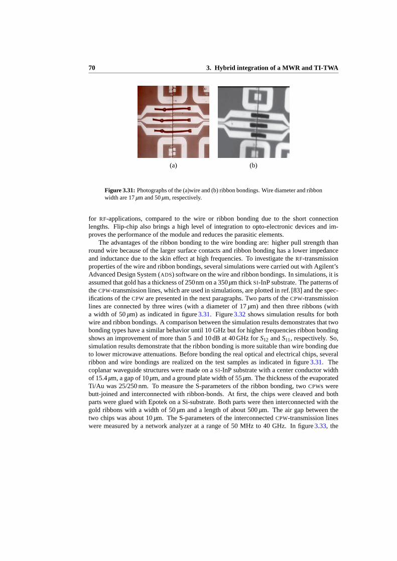
70 3. Hybrid integration of a MWR and TI-TWA
(a) (b)
Figure 3.31: Photographs of the (a)wire and (b) ribbon bondings. Wire diameter and ribbonwidth are 17µm and 50µm, respectively.
for RF-applications, compared to the wire or ribbon bonding due to the short connectionlengths. Flip-chip also brings a high level of integration to opto-electronic devices and im-proves the performance of the module and reduces the parasitic elements.
The advantages of the ribbon bonding to the wire bonding are: higher pull strength thanround wire because of the larger surface contacts and ribbon bonding has a lower impedanceand inductance due to the skin effect at high frequencies. To investigate theRF-transmissionproperties of the wire and ribbon bondings, several simulations were carried out with Agilent’sAdvanced Design System (ADS) software on the wire and ribbon bondings. In simulations, it isassumed that gold has a thickness of 250nm on a 350µm thickSI-InP substrate. The patterns oftheCPW-transmission lines, which are used in simulations, are plotted in ref. [83] and the spec-ifications of theCPW are presented in the next paragraphs. Two parts of theCPW-transmissionlines are connected by three wires (with a diameter of 17µm) and then three ribbons (witha width of 50µm) as indicated in figure3.31. Figure3.32 shows simulation results for bothwire and ribbon bondings. A comparison between the simulation results demonstrates that twobonding types have a similar behavior until 10 GHz but for higher frequencies ribbon bondingshows an improvement of more than 5 and 10 dB at 40 GHz forS12 andS11, respectively. So,simulation results demonstrate that the ribbon bonding is more suitable than wire bonding dueto lower microwave attenuations. Before bonding the real optical and electrical chips, severalribbon and wire bondings are realized on the test samples as indicated in figure3.31. Thecoplanar waveguide structures were made on aSI-InP substrate with a center conductor widthof 15.4µm, a gap of 10µm, and a ground plate width of 55µm. The thickness of the evaporatedTi/Au was 25/250 nm. To measure the S-parameters of the ribbon bonding, twoCPWs werebutt-joined and interconnected with ribbon-bonds. At first, the chips were cleaved and bothparts were glued with Epotek on a Si-substrate. Both parts were then interconnected with thegold ribbons with a width of 50µm and a length of about 500µm. The air gap between thetwo chips was about 10µm. The S-parameters of the interconnectedCPW-transmission lineswere measured by a network analyzer at a range of 50 MHz to 40 GHz. In figure3.33, the

3.6 Mounting and bonding 71
0 10 20 30 40−40
−30
−20
−10
0
Frequency (GHz))
S−
para
met
er (
dB)
Figure 3.32: S-parameters of the simulated wire and ribbon bondings. “♦” (S12) and “©”(S11) are simulation results for ribbon bonding and the solid lines are simulation results forwire bonding.
0 10 20 30 40−40
−30
−20
−10
0
Frequency (GHz))
S−
para
met
er (
dB)
Figure 3.33: S-parameters of the simulated and measured ribbon bondings. “♦” (S12) and“©” (S11) are simulation results and the solid lines are measurement results.

72 3. Hybrid integration of a MWR and TI-TWA
Figure 3.34: (left) The realized hybrid integrated receiver with the optical chip in the mid-dle and theTI-TWAs on both sides. (right) A microscope photograph of the ribbon bondingswhich connect the bond-pads (GSG) of a photodetector to theTI-TWA.
measurement results ofS11 andS12 for ribbon bonding are presented. The simulation resultsare shown on the same plot to compare the simulated and measured results. They show a goodagreement e.g. less than 2dB forS12 at 40 GHz.
In conclusion, the comparison between simulation results of wire and ribbon bondings andsimulated and measured results of the ribbon bondings, shows that ribbon bonding has a betterRF-behavior at frequencies over 10GHz and is suitable up to 40 GHz.
3.7 Hybrid integrated MWR and TI-TWA
In figure3.34-left, a realized hybrid integrated receiver is shown. It consists of an opticalreceiver in middle and sixTI-TWAs in both sides. The hybrid integrated receiver is mountedand glued with a conductive epoxy on a copper submount (the schematic view of submountis depicted in figure3.29). The photodectors andTI-TWAs were then connected by ribbonbonds, with a width of 40µm and a length of about 300µm (see figure3.34-right). The widthof ribbon heel on the probe-pad is usually broadened under pressure of the bonding machine.As indicated in figure3.34, six of the eight photodetectors are bonded to theTI-TWAs. Thisallows us to characterize both adjacent and opposite channels, which may show differentRF-crosstalk. Two photodetectors were not connected and were used to align the fiber-tip to theinput waveguide and for finding the wavelength of each channel.
The integratedWDM receiver is characterized by a light-wave component analyzer. Thesetup is similar to the setup which is used to characterize the optical-part of theWDM-receiver.An external tunable laser source is used, which causes the light-wave component analyzer tooperate at a wavelength window around 1.55µm. A bias-tee is not needed in this setup, as the

3.8 Conclusion 73
0 5 10 15 20 25−10
−8
−6
−4
−2
0
Frequency (GHz)
Nor
mal
ized
freq
uenc
y re
spon
se (
dB)
Figure 3.35: The measured frequency response of three channels in the hybrid integratedWDM receiver.
DC bias-voltage for the photodetectors is provided by theTI-TWA. For this, in addition to theRF-probe on the amplifier, three needles are employed to apply the bias voltages of drain, gateand photodetector of 6 V,−0.45 V, and 5 V, respectively. The bias voltages of drain, gate andphotodetectors are slowly increased and measured with three volt meters while simultaneouslymeasuring the current of each pad three current meters to monitor the current. Without thebias-tee, the calibration of the setup becomes simpler. The normalized frequency response ofthree channels is presented in figure3.35. The frequency response of the best channel shows abandwidth over 20 GHz and the two other channels have bandwidths of about 18GHz .
3.8 Conclusion
We have described the design and realization of a hybrid integratedWDM receiver for a high-speed communication network. We first presented the design, realization and characterizationof an eight-channel, polarization independent opticalMWR with a bandwidth around 23 GHz.A submount was fabricated to mount the optical-MWR chip andTI-TWAs. Then, several ex-periments on ribbon- and wire bondings were carried out, showing that ribbon bonding has abetter electrical behavior compared to wire bonding at frequencies above 10GHz. In addition,the TI-TWAs were characterized and a bandwidth of about 33 GHz was measured, which issuitable for a 40 Gb/s receiver. Finally, the opticalMWR and sixTI-TWAs were mounted andbonded. Three channels were characterized and the best channel showed a bandwidth of over20GHz. For 40Gb/s operation it is required to improve the bandwidth of the twin-WGPDs. Our

74 3. Hybrid integration of a MWR and TI-TWA
results are close to the best results reported so far: 25 GHz bandwidth for a twin-guide MWRwithout integrated front-end amplifier [84] .

Chapter 4
Waveguide pin-photodetector
This chapter describes the design and characterization of awaveguide pin-photodetector (WGPD)based on butt-joint integration of a transparent waveguide and a detector based on a reverselybiased Semiconductor Optical Amplifier(SOA). DC-measurements on short SOA-sections havedemonstrated that the SOA can be utilized as a photodetector. In this chapter, the static andhigh-frequency behavior of the photodetector are investigated and characterized.
4.1 Introduction
An important issue in the design of a photodetector is choosing a material which has sufficientabsorption at the operation wavelength. The detector is designed for use at a wavelength of1.55µm since the optical fiber propagation loss is minimal at that wavelength. The bandgapwavelengthλg of In1−xGaxAsyP1−y material that is lattice matched to the InP substrate is be-tween 0.92µm and 1.65µm for y varying fromy= 0 toy= 1, so that it is suitable for use in the1.55µm wavelength window. For convenience, quaternary material with a bandgap wavelengthof, for example,λg = 1.25µm is referred to as Q(1.25).
A passive ridge waveguide consists of a guiding layer embedded between cladding layers.Confinement of the light in the transversal direction is obtained by the guiding layer with ahigher refractive index with respect to the cladding layers. InP is used for the cladding layers,which have a refractive index of 3.17 at a wavelength of 1.55µm. By changing the compositionof the quaternary InGaAsP material, the index of refraction can be chosen between that of InP(nInP = 3.17, λ = 1.55µm) and Q(1.55) (nQ(1.55) ≈ 3.55, λ = 1.55µm). A larger index contrastbetween guiding layer and cladding/buffer layers increases the optical confinement, as wellas the electro-optical effect, which is used in phase shifters. We use Q(1.25), which givessufficient optical confinement and electro-optical effect and is sufficiently far from the bandedge of Q(1.55), where the light is absorbed. Confinement of the light in the lateral direction
75
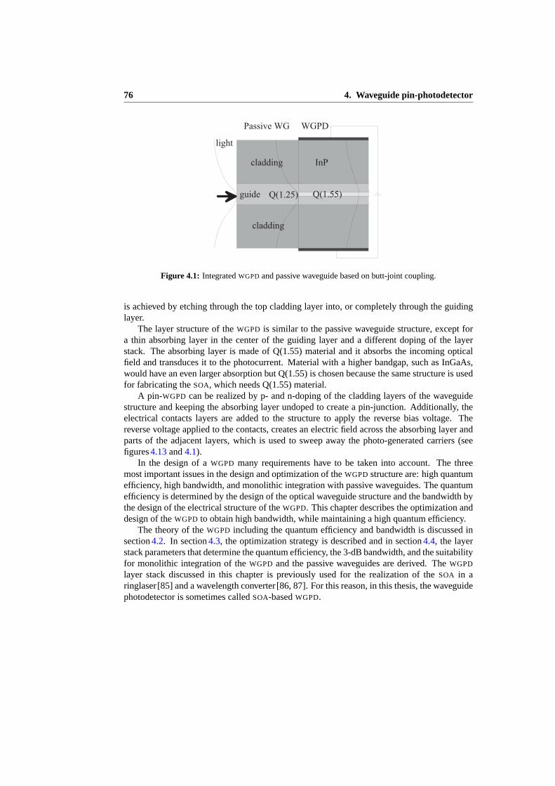
76 4. Waveguide pin-photodetector
g u i d e
c l a d d i n g
c l a d d i n g
Q ( 1 . 5 5 )
P a s s i v e W G W G P Dl i g h t
Q ( 1 . 2 5 )
I n P
Figure 4.1: IntegratedWGPD and passive waveguide based on butt-joint coupling.
is achieved by etching through the top cladding layer into, or completely through the guidinglayer.
The layer structure of theWGPD is similar to the passive waveguide structure, except fora thin absorbing layer in the center of the guiding layer and a different doping of the layerstack. The absorbing layer is made of Q(1.55) material and it absorbs the incoming opticalfield and transduces it to the photocurrent. Material with a higher bandgap, such as InGaAs,would have an even larger absorption but Q(1.55) is chosen because the same structure is usedfor fabricating theSOA, which needs Q(1.55) material.
A pin-WGPD can be realized by p- and n-doping of the cladding layers of the waveguidestructure and keeping the absorbing layer undoped to create a pin-junction. Additionally, theelectrical contacts layers are added to the structure to apply the reverse bias voltage. Thereverse voltage applied to the contacts, creates an electric field across the absorbing layer andparts of the adjacent layers, which is used to sweep away the photo-generated carriers (seefigures4.13and4.1).
In the design of aWGPD many requirements have to be taken into account. The threemost important issues in the design and optimization of theWGPDstructure are: high quantumefficiency, high bandwidth, and monolithic integration with passive waveguides. The quantumefficiency is determined by the design of the optical waveguide structure and the bandwidth bythe design of the electrical structure of theWGPD. This chapter describes the optimization anddesign of theWGPD to obtain high bandwidth, while maintaining a high quantum efficiency.
The theory of theWGPD including the quantum efficiency and bandwidth is discussed insection4.2. In section4.3, the optimization strategy is described and in section4.4, the layerstack parameters that determine the quantum efficiency, the 3-dB bandwidth, and the suitabilityfor monolithic integration of theWGPD and the passive waveguides are derived. TheWGPD
layer stack discussed in this chapter is previously used for the realization of theSOA in aringlaser [85] and a wavelength converter [86, 87]. For this reason, in this thesis, the waveguidephotodetector is sometimes calledSOA-basedWGPD.

4.2 WGPD quantum efficiency and bandwidth 77
Heinrich Hertz Institute recently reported a receiver with a bandwidth up to 110 GHz [88]and a responsivity of 0.73A/W at 1.55µm wavelength. This photodetector has been monolith-ically integrated with a traveling wave amplifier and a circularly-toothed planar logarithmic-periodic antenna. The dimensions of the photodetector are 5× 20µm. Integration of thesedetectors withAWGs in aMWR has not yet been reported.
4.2 WGPD quantum efficiency and bandwidth
When an optical field propagates through theWGPD, it is absorbed and generates electron-hole pairs if the photons have an energy larger than the semiconductor bandgap. The currentgenerated in the absorption layer and in the adjacent layers, consists of two parts: a drift currentoriginating from the electron-hole pairs created in the depletion layer, and a diffusion currentoriginating from the photo-excited carriers generated outside the depletion layer. Because thediffusion velocity is much smaller than the drift velocity it causes a long trailing edge at theend of each pulse which increases the interference between different pulses and hence the Bit-Error Rate (BER). It can be avoided by completely depleting the absorption layer, where thecarriers are generated.
Three types of photon absorption or loss can occur in the intrinsic and the adjacent layers[60]: interband absorption (αIB), free-carrier absorption (αFC) and scattering loss (αS). TheαS and theαFC result from loss of photons without generation of carriers. Usually, the activeregion has a low doping level and it is allowed to neglectαFC. TheαS is due to irregularitiesat the interfaces of the layers or the side-wall of the mesa. Because only part of the fieldpropagates in the absorption layer,αIB is reduced by the confinement factorΓ. Therefore, theabsorbed photons that generate the photo-current are described by the extinction coefficientΓαIB .
The total amount of power absorbed in the Q(1.55) semiconductor as a function ofz isgiven by [89]:
Pabs(z) = Pinηin(1−R)ΓαIB
α(1−e−αz) (4.1)
wherePin is the incident power,l is the length of theWGPD, R is the reflection coefficient onthe facet of the chip and the air,ηin is the fiber to chip coupling efficiency, andα is the totalloss coefficient, given by
α = ∑i
(ΓiαIB +ΓiαFCi +(1−Γi)αFCx+αSi) (4.2)
whereΓi , αFCi , andαsi are the confinement factor, the free-carrier absorption loss, and thescattering loss in theith layer. The external quantum efficiency of theWGPD can be obtainedfrom:
ηext =Pabs
Pin= ηin(1−R)
ΓαIB
α(1−e−αl ) (4.3)

78 4. Waveguide pin-photodetector
SinceΓαIB αFC,αFCi,αS, eq.4.3simplifies to the more familiar expression
ηext = ηin(1−R)(1−e−αl )
The responsivity of theWGPD is the ratio of the generated current to the incident optical power.
ℜ =Iph
Pin=
eλhc
ηin(1−R)(1−e−αl ) (4.4)
whereIph is the generated photo-current,λ is the wavelength,e is the electron charge,h isPlank’s constant, andc is the speed of light.
There are several limitations to the bandwidth of theWGPD which are due to the junctionRC-elements [90], the drift transit time, the diffusion transit time, and the charge trapping atthe heterojunctions as discussed in chapter2 for the twin-WGPD.
In theWGPD structure, to avoid charge trapping, several changes with respect to the twin-WGPD structure described in Chapter 2 are carried out. The absorption layer, Q(1.55), is sur-rounded by two Q(1.25) layers which have a bandgap wavelength between the InP claddingand the Q(1.55) absorbing layers. For the n-contact side in order to lower the n-contact resis-tance, a thin layer of highly n-doped InGaAs is placed on the highly-doped n-InP layer whichfunctions as a contact layer to reduce contact resistance.
4.3 Optimization strategy
So far, the basic features and concepts of theWGPD have been discussed. In the followingsections, we focus on the optimization strategy which is carried out. The main optimizationparameters of theWGPD are: the thickness of the guiding and cladding layers, the width andlength of the ridge, and the doping level of the layers.
To design a high-speed and high-efficiencyWGPD, trade-offs between the main parametersare necessary. High-efficiency requires a long and wideWGPD that causes an increase of thejunction capacitance and, consequently, degradation of the theRC-bandwidth. The thicknessof the cladding layers has to be sufficient to prevent absorption of the optical mode in theInGaAs p-contact layers and the metal. However a thick cladding layer gives rise to increasedseries resistance and a decreasingRC-bandwidth. If the active layer thickness increases, ahigher quantum efficiency with a shorter length is possible. For a small transit time a thinactive layer is required, however. A high-doping level for the p-cladding and the n-buffer isrequired to obtain a low-series resistance, but it increases the optical loss. In the followingsubsections, the effects of these parameters on the quantum efficiency and theRC- and transittime bandwidths are investigated.
4.4 Optical and electrical design of the WGPD
In the design and optimization of theWGPD geometry, several requirements have to be ful-filled. The layer thickness and doping profile of the layers, and the width and length of the

4.4 Optical and electrical design of the WGPD 79
S I - I n Pn + + - I n P
p - - I n P
p + + - I n P
n + - I n P
p + + - I n G a A sA u
A uA ui - Q ( 1 . 2 5 )i - Q ( 1 . 2 5 )i - Q ( 1 . 5 5 )
d p
d id n
W
L n
yx
p + - I n Pp - I n P
Figure 4.2: Schematic cross-section of theWGPD used in the optical and electrical design.W = 2µm, dp= 1300 nm,dn= 200 nm, anddi= 500 nm.
WGPD are major parameters to design a high-speed and high-quantum efficiencyWGPD. Inthis section, the effects of parameters on theWGPD performance is investigated. The crosssection of theWGPD which is used to derive the optimal configuration suitable for the fabri-cation process is shown in figure4.2. As stated in the previous sections, three main issues inthe design of the optimalWGPD are the quantum efficiency, the bandwidth, and the monolithicintegration with the passive waveguide. The quantum efficiency is determined by the opticaldesign (subsection4.4.1), the bandwidth by the electrical design (subsection4.4.2), and the in-tegration of theWGPD and a passive waveguide requires careful consideration of the dopingprofile and layer stack thickness (subsection4.4.3).
4.4.1 Optical design
One of the most important parameters in the determination of the quantum efficiency (eq.4.3) isthe optical attenuation in the Q(1.55) bulk material. In order to determine the optical absorptionof the Q(1.55) material, the absorption of severalSOAs with different lengths, 2µm width, anda 120 nm thick Q(1.55) has been measured. The layer structure of theWGPD is identicalto the SOA structure that is previously used in the multi-wavelength ring laser [85]. Opticalpower is launched from anEDFA into the reversely biasedSOA. A part of the incident power

80 4. Waveguide pin-photodetector
0 100 200 300
−60
−40
−20
0
Length (µm)
Atte
nuat
ion
(dB
)
Figure 4.3: Attenuation vs. length for aSOA-section measured at a wavelength of 1.55µmunder different bias voltages (0, –2.5, and –5Vs). ; The solid curve is a trend line.
is absorbed by theSOA and the transmitted power is measured at the output facet by anOSA
instrument. The difference between the measured and the incident optical power gives us theabsorption of theSOA-section. In figure4.3, the optical attenuation for the different lengths ofthe SOA, measured at a wavelength of 1.55µm is shown, form which we findΓα = 250/cm.The confinement of the optical power in the 120 nm thick active layer is about 27% whichgives us for the bulk absorption of the Q1.55 materialα = 930/cm.
Based on equation4.1, three methods are possible for increasing the quantum efficiency:increasing the length of the detector (l ), increasing the field confinement in the active material(Γ) by increasing the thickness of the active layer in the transversal direction or by increasingtheWGPD width in the lateral direction, and increasing the interband absorption (αIB).
The effect of the detector length and the active layer thickness on the quantum efficiencycan be seen in figure4.4-a, the quantum efficiency can be increased by increasing the length(with a constant active layer thickness) or by increasing the active layer thickness (with aconstant length).
In this dissertation, we use theWGPD in a Multi-Wavelength Receiver (MWR,see chapter5).The MWR operates in the wavelength window from 1530 nm to 1560 nm. Consequently, thequantum efficiency variation of theWGPDs has to be investigated in this wavelength range. Inorder to determine the variations of the quantum efficiency, the optical attenuation of theSOA
structure has been measured as a function of wavelength at 0,−2.5, and−5V bias voltage. Thequantum efficiency versus wavelength (figure4.4-b) has been calculated using eq.4.3. Withincreasing reverse bias voltage, the dependence of the absorption on wavelength is reduced.
Moreover, in accordance with the scattering matrix (SMM) method, the optical power as afunction of the length of theWGPD is determined and shown in figure4.5-b for both theTE andTM modes. According to figure4.5-a, a length of 60µm is sufficient for 90% internal quantumefficiency. These results are in a good agreement with figure4.4. The refractive index of the

4.4 Optical and electrical design of the WGPD 81
0.1 0.1 0.1
0.2
0.2 0.2 0.2
0.3
0.30.3 0.3
0.4
0.4
0.40.4
0.50.5
0.5
0.5 0.5
0.6
0.6
0.6
0.6 0.6
0.7
0.7
0.7
0.7
0.8
0.8
0.8
0.8
0.9
0.9
0.9
0.9
1
1
1
Active layer thickness (µm)
Leng
th (
µm)
0.1 0.2 0.3 0.4 0.5
20
40
60
80
100
1520 1530 1540 1550 1560
0.7
0.8
0.9
1
wavelength (µm)
Inte
rnal
qua
ntum
effi
cien
cy
0 V
−2.5 V
−5 V
(a) (b)
Figure 4.4: (a) Internal quantum efficiency as a function of the active layer thickness anddetector length for aWGPD with 2µm width. (b) Quantum efficiency vs. wavelength for a60µm longWGPD at three different reverse bias voltages of 0,−2.5, and−5 volts.
0 50 1000
0.2
0.4
0.6
0.8
1
z−position (µm)
Nor
mal
ized
opt
ical
pow
er
TE
TM
0 50 1000
2
4
6
8
WGPD length (µm)
Cur
rent
(a.
u.)
TE
TM
(a) (b)
Figure 4.5: (a) Normalized optical power as a function of z-position (propagation direc-tion). (b) Generated photocurrent as a function of z-position forTE andTM modes.
Q(1.55)-material is assumed to ben = 3.55− j0.021. In figure4.5-a, the generated photo-current vs. photodetector length is determined which shows that for aWGPD with a lengthvarying from 50 to 100µm, the increase in the photocurrent is less than 10%. The normalizedpower distribution is plotted for a 100µm long device (see figure4.6). It shows that the majorpart of the power is in the guiding layers (Q(1.55) and Q(1.25) layers) .

82 4. Waveguide pin-photodetector
0.1
0.1
0.1
0.1
0.1
0.2
0.2
0.2
0.20.3
0.3
0.3
0.4
0.4
0.5
0.50.6
0.7
0.8
0.9
x−position (µm)
Leng
th (
µm)
−0.5 0 0.5 1 1.5 20
20
40
60
80
100
0.1
0.1
0.1 0.1
0.1
0.1
0.2
0.2
0.2
0.2
0.2
0.3
0.3
0.3
0.4
0.4
0.4
0.5
0.5
0.6 0.6
0.7
0.8
0.9
x−position (µm)
Leng
th (
µm)
−0.5 0 0.5 1 1.5 20
20
40
60
80
100
(a) (b)
Figure 4.6: Normalized optical power as a function of length and y-position for theTE (a)andTM (b) mode. Positionx = 0 is defined in figure4.2.
4.4.2 Electrical design
Based on expressions2.20and2.24, the main parameters that determine theRC- and transit timebandwidths are: the series resistances (Rp, Rn, RC,P), the junction capacitance (Cpd), and thedepletion layer thickness (di) as shown in figure4.7. To increase theRC-bandwidth the seriesresistance and the junction capacitance have to be reduced. In order to decrease the seriesresistance, it is required to increase the doping levels of the p-doped cladding and the n-dopedbuffer layer or to increase the width or the length of the p-mesa. The junction capacitance ofthe WGPD can be reduced by increasing the depletion layer thickness and by decreasing thewidth and the length of theWGPD. Based on eq.2.20, a 45 GHz transit time bandwidth of theWGPDwith avsat,p = 4×106 cm/s anddi = 500nm is predicted. In figure4.8, the effects of thevarious parameters of theWGPD including ridge width, n-substrate thickness, 500 nm lowerp-InP cladding layer thickness and doping, film layer thickness, and the lengthLnof the lateraln-type current channel on theRC- bandwidth are shown as determined by using eq.2.29. Thenthe total bandwidth can be determined by eq.2.30. By increasing the ridge width of theWGPD
from 1µm to 4µm, theRC-bandwidth reduces from 110GHz to 50GHz and the total bandwidthdrops about 10 GHz. The thickness of the n-buffer layers has no much influence on theRC-bandwidth shown in figure4.8-b. The effect of the doping level of the cladding layers on thebandwidth is important and shown in figure4.8-c. By increasing the doping level from 1e16 to1e19 /cm3 the conductivity increases exponentially and the series resistance Rp decreases, sotheRC-bandwidth increases more than 60GHz and the total bandwidth improves about 15GHz.However, this also increases the optical attenuation, therefore the doping level of the claddingsis graded. The cladding thickness should be sufficiently thick to keep the optical attenuationlow but it increases the series resistanceRp . We have chosen a graded doping level with a total1500 nm cladding layer thickness to reach to about 40 GHz total bandwidth.
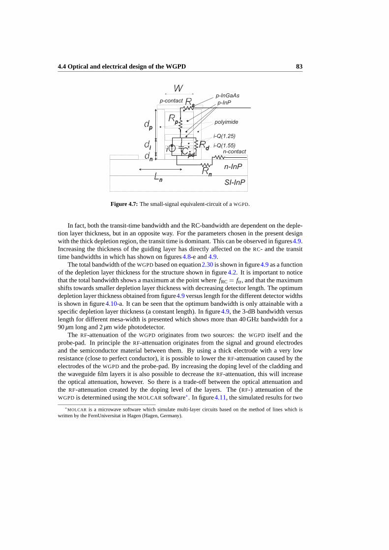
4.4 Optical and electrical design of the WGPD 83
S I - I n P
p - I n Pp - I n G a A sp - c o n t a c t
n - c o n t a c tin - I n P
i - Q ( 1 . 2 5 )i - Q ( 1 . 5 5 )
p o l y i m i d e
Figure 4.7: The small-signal equivalent-circuit of aWGPD.
In fact, both the transit-time bandwidth and the RC-bandwidth are dependent on the deple-tion layer thickness, but in an opposite way. For the parameters chosen in the present designwith the thick depletion region, the transit time is dominant. This can be observed in figures4.9.Increasing the thickness of the guiding layer has directly affected on theRC- and the transittime bandwidths in which has shown on figures4.8-e and4.9.
The total bandwidth of theWGPDbased on equation2.30is shown in figure4.9as a functionof the depletion layer thickness for the structure shown in figure4.2. It is important to noticethat the total bandwidth shows a maximum at the point wherefRC = ftr, and that the maximumshifts towards smaller depletion layer thickness with decreasing detector length. The optimumdepletion layer thickness obtained from figure4.9versus length for the different detector widthsis shown in figure4.10-a. It can be seen that the optimum bandwidth is only attainable with aspecific depletion layer thickness (a constant length). In figure4.9, the 3-dB bandwidth versuslength for different mesa-width is presented which shows more than 40 GHz bandwidth for a90µm long and 2µm wide photodetector.
The RF-attenuation of theWGPD originates from two sources: theWGPD itself and theprobe-pad. In principle theRF-attenuation originates from the signal and ground electrodesand the semiconductor material between them. By using a thick electrode with a very lowresistance (close to perfect conductor), it is possible to lower theRF-attenuation caused by theelectrodes of theWGPD and the probe-pad. By increasing the doping level of the cladding andthe waveguide film layers it is also possible to decrease theRF-attenuation, this will increasethe optical attenuation, however. So there is a trade-off between the optical attenuation andthe RF-attenuation created by the doping level of the layers. The (RF-) attenuation of theWGPD is determined using theMOLCAR software∗. In figure4.11, the simulated results for two
∗MOLCAR is a microwave software which simulate multi-layer circuits based on the method of lines which iswritten by the FernUniversitat in Hagen (Hagen, Germany).

84 4. Waveguide pin-photodetector
4 0
6 0
8 0
1 0 0
1 0 0 0 2 0 0 0 3 0 0 0 4 0 0 0W i d t h ( n m )
RC b
andw
idth (
GHz)
7 5
7 5 . 5
7 6
7 6 . 5
4 0 0 8 0 0 1 2 0 0 1 6 0 0n - I n P s u b s t r a t e t h i c k n e s s ( n m )
RC ba
ndwi
dth (G
Hz)
(a) (b)
3 0
5 0
7 0
9 0
1 E + 1 6 1 E + 1 7 1 E + 1 8 1 E + 1 9
p - I n P c l a d d i n g d o p i n g l e v e l ( c m - 3 )
RC ba
ndwid
th (G
Hz)
6 0
7 0
8 0
9 0
0 4 0 0 8 0 0 1 2 0 0 1 6 0 0C l a d d i n g t h i c k n e s s ( n m )
RC ba
ndwid
th (G
Hz)
(c) (d)
4 0
6 0
8 0
1 0 0
1 2 0
3 0 0 5 0 0 7 0 0f i l m t h i c k n e s s ( n m )
RC ba
ndwid
th (G
Hz)
6 8
7 3
7 8
0 1 0 0 0 0 2 0 0 0 0L n ( n m )
RC ba
ndwid
th (G
Hz)
(e) (f)
Figure 4.8: The RC bandwidths of theWGPD as function of the a) width, b) n-InP bufferlayer thickness, c)p-InP cladding doping level d) lower p-InP cladding thickness e) guidinglayer thickness f)Ln. For each figure, the parameters that are kept constant, are accordingto the values shown in figure4.2.

4.4 Optical and electrical design of the WGPD 85
0 500 1000 15000
20
40
60
80
Depletion layer thickness (nm)
Ban
dwid
th (
GH
z)
10µm
60µm
300µm
0 100 200 30010
20
30
40
50
Length (µm)B
andw
idth
(G
Hz)
1µm
2µm
3µm
4µm
(a) (b)
Figure 4.9: (a) Bandwidth as a function of the depletion layer thickness for three differentlengths and 2µm width. (b) Bandwidth as a function of length for various widths and adepletion layer thickness of 500 nm.
0 100 200 300200
400
600
800
1000
1200
Length (µm)Opt
imum
dep
letio
n th
ickn
ess
(nm
)
3µm 2µm 1µm4µm
0 100 200 3000
20
40
60
80
Length (µm)
Opt
imum
ban
dwid
th (
GH
z)
1µm2µm3µm4µm
(a) (b)
Figure 4.10: (a) Optimum layer thickness vs. length for various widths. (b) Optimumbandwidth vs. length for various widths.

86 4. Waveguide pin-photodetector
0 10 20 30 400
2
4
6
8
10
Frequency (GHz)
RF
−at
tenu
atio
n (d
B/m
m)
1 µm
2 µm
Figure 4.11: TheRF-attenuation of theWGPD for 1 and 2µm wide ridge. In the simulations,the width of the signal electrode has been taken 1µm wider than ridge and the thickness ofthe gold in the signal and ground electrodes is considered 1.5µm.
photodetectors with ridge widths of 1µm and 2µm is shown. The width of the signal-electrodeat top of the p-contact is taken 1µm wider than ridge width, which is determined by the electro-plating process that is used. The attenuation of the generatedRF-signal in a 100µm longWGPD
is less than 0.8dB at 40GHz. TheRF-attenuation can be further reduced by reducing the ridgewidth. A wider ridge leads to a larger junction capacitance and, consequently, largerRF-currents to charge it. These larger currents will produce largerRF-losses due to the resistanceof the doped cladding layers. To achieve a lowRF-attenuation it is important that the goldelectrodes are sufficiently thick. This can be achieved by electro-plating [91].
In figure4.12-d & -c, the cross-section and top-view of the probe-pad are shown, respec-tively. The probe-pad electrodes are placed on a polyimide layer. TheRF-attenuation andimpedance of the probe-pad is determined using theADS (Momentum) software which cal-culates these parameters by discretizing the region and solving the Maxwell’s equation in thenodes of each mesh. Figure4.12-b shows that theRF-attenuation is very low (less than 0.1 dBat 40GHz) due to the very low conductivity of the polyimide andSI-InP. The impedance curve(figure4.12-a) shows a low value of about 13Ω up to 40 GHz. The low value is caused bythe transition part between the probe-pad and the detector. This impedance creates a 58%mismatch between the probe pad impedance (50Ω) and the photodetector impedance.
4.4.3 Monolithic integration of the WGPD with passive waveguide
The layer structures in the detector section and in the passive waveguide sections are shownin Figure4.13. As can be seen from the figure many layers are shared between the active andthe passive sections: all substrate layers and most of the upper cladding layers, except for athin InP-layer directly on top of the waveguide, which is undoped (non-intentionally doped)

4.4 Optical and electrical design of the WGPD 87
0 10 20 30 400
10
20
30
40
50
Impe
danc
e (Ω
)
Frequency (GHz)0 10 20 30 40
0
0.05
0.1
0.15
0.2
RF
−at
tenu
atio
n (d
B)
Frequency (GHz)
(a) (b)
1 0 0 m m
5 0 m m
5 0 m m
1 0 0 m m
5 0 m m
1 0 m m2 m m
S I - I n Pn + + - I n P p o l y i m i d e
A u 1 . 5 m m3 m m
(c) (d)
Figure 4.12: (a) impedance of the probe-pad. (b)RF-attenuation of the probe-pad. (c) Top-view of the probe-pad. (d) Cross-section of the probe-pad on the polyimide layers and theSI-InP substrate.

88 4. Waveguide pin-photodetector
S I - I n Pn + + - I n P
i - Q ( 1 . 2 5 )p - I n Pp + - I n Pp + + - I n P
n + - I n Pi - I n P
i - Q ( 1 . 5 5 )
p + + - I n G a A sA c t i v e p a s s i v e
1 0 0 0 m m
1 0 0 0 m m
7 5 0 m m
5 0 0 m m
5 0 0 m m
7 5 0 m m
2 0 m m
1 5 0 0 m m
2 0 m m
1 5 0 0 m m
(a) (b)
Figure 4.13: (a) layer stack of the active and passive parts of aSOA. More details are intable4.1 (b) Top view of the active-passive mask that is used to define the active regions.The width of each stripe is 20µm.
in the passive section in order to keep the propagation loss low, and highly doped in the activesection in order to keep the series resistance for the detector low. Because it is the aim of thispart of thesis to use a reversely biased SOA as a detector and to remain compatible with theactive-passive integration process used for other applications, the freedom in the choice of thelayer stacks is limited. In this section we will analyse the performance of the active-passiveintegration process for detector applications and we will study how the design of the detectorcan be optimized. The main trade-offs that have to be made are between the series resistancesof the detector, which requires high doping levels and thin cladding layers, and the opticalpropagation loss of the passive waveguides, which requires a low doping level and thickercladding layers in order to keep the light away from the highly doped layers. Next subsectionsdescribe these trade-offs and discuss a compromise between them.
Cladding layer
Optical losses are much higher in p-doped material than in n-doped material, so the doping pro-file of the upper p-doped cladding layer is most important for the design of the monolithicallyintegrated detector. The p-doped upper cladding serves for optical confinement of the lightin the waveguide and it forms the electrical channel for carrying the current generated in theabsorption layer to the outside world. The upper cladding consists of a number of InP-layers

4.4 Optical and electrical design of the WGPD 89
0.6 0.8 1 1.2 1.40
1
2
3
4
Cladding thickness (µm)
Abs
orpt
ion
(dB
/cm
)
Figure 4.14: Absorption of the optical field in the InGaAs contact layer as a function ofthe cladding thickness for a 200 nm thick InGaAs contact layer and aW=2µm wide (seefigure4.2).
with a stepwise increasing doping level and a highly doped InGaAs layer on top. The InGaAslayer is required to form a good electrical contact to the metal layer on top of the detector. Ithas a higher index than the waveguide layer and is highly absorptive (nInGaAs= 3.7− j0.28).Therefore, the thickness of the InP cladding layers has to be sufficient to isolate the waveguidefrom the InGaAs layer and keep the absorption of the guided mode in this layer sufficientlysmall. Figure4.14shows the optical propagation loss of the guided mode in the detector wave-guide with a 200 nm InGaAs contact layer as a function of the InP cladding layer thickness.As the absorption losses in a detector are typically in the order of 1000 dB/cm, it is seen thatan InP layer thickness larger than 500 nm is sufficient for keeping the losses in the top InGaAslayer negligible.
Absorption in the p-doped InP cladding is a major source of loss in the transparent wave-guide sections. The dominant absorption mechanism for p-InGaAsP material (including p-InPmaterial) is intra-valence band absorption, which is given by [92]:
αP = 9.9×10⁻¹⁷p dB/cm (4.5)
for λ = 1.55µm and 1016 < p < 1019 cm−3.Figure4.15 shows the optical loss and the electrical resistance against the doping level
in the p-doped InP cladding. It can be seen that the resistance increases from a few ohms atp= 1×10¹⁸/cm3 to a tens of ohms atp= 1×10¹⁷/cm3 doping level. An optimal compromisebetween low loss and low resistance is obtained by using a graded doping profile, where thedoping starts at a low level close to the waveguide layer, and increases in layers that are furtheraway of the guided mode. More than 95% of the optical power is confined in a region thatextends 200 nm on both sides of the waveguide layers. By keeping the first 200 nm of thetop-cladding in the passive waveguide sections undoped (or n.i.d), a low optical attenuation isattainable. In theWGPD, a 200 nm n.i.d InP cladding layer will create an additional resistanceabout 100Ω for a 60µm long photodetector. Therefore, in the detector section an InP layer
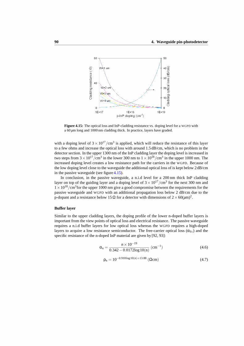
90 4. Waveguide pin-photodetector
Figure 4.15: The optical loss and InP-cladding resistance vs. doping level for aWGPDwitha 60µm long and 1000 nm cladding thick. In practice, layers have graded.
with a doping level of 3×10¹⁷/cm3 is applied, which will reduce the resistance of this layerto a few ohms and increase the optical loss with around 1.5dB/cm, which is no problem in thedetector section. In the upper 1300 nm of the InP cladding layer the doping level is increased intwo steps from 3×10¹⁷/cm3 in the lower 300 nm to 1×10¹⁸/cm3 in the upper 1000 nm. Theincreased doping level creates a low resistance path for the carriers in theWGPD. Because ofthe low doping level close to the waveguide the additional optical loss of is kept below 2dB/cmin the passive waveguide (see figure4.15).
In conclusion, in the passive waveguide, a n.i.d level for a 200 nm thick InP claddinglayer on top of the guiding layer and a doping level of 3×10¹⁷/cm3 for the next 300 nm and1×1018/cm3for the upper 1000 nm give a good compromise between the requirements for thepassive waveguide andWGPD with an additional propagation loss below 2 dB/cm due to thep-dopant and a resistance below 15Ω for a detector with dimensions of 2×60(µm)2.
Buffer layer
Similar to the upper cladding layers, the doping profile of the lower n-doped buffer layers isimportant from the view points of optical loss and electrical resistance. The passive waveguiderequires a n.i.d buffer layers for low optical loss whereas theWGPD requires a high-dopedlayers to acquire a low resistance semiconductor. The free-carrier optical loss (αFc) and thespecific resistance of the n-doped InP material are given by [92, 93]:
αn =n×10−19
0.342−0.0172log10(n)(cm−1) (4.6)
ρn = 10−0.918log10(n)+13.88 (Ωcm) (4.7)

4.5 Fabrication Technology 91
for doping levels of 1016 < n < 1018 cm−3.An optimal trade-off between low optical loss in the passive waveguide and low resistance
in theWGPD is made by choosing a graded doping level for the n-doped buffer layer. The firstInP buffer layer below the guiding layer is n-doped with a thickness of 200 nm and a dopinglevel of 5×10¹⁷/cm3 and the second layer has a thickness of 900 nm and a doping level of1×1018/cm3.
Guiding layer
Based on figures4.8and4.9, a good control of the depletion layer thickness is required in theWGPD to obtain a maximum bandwidth. i.e. for a 1µm wide and 90µm long device, a 300 nmthick depletion layer is required to obtain more than 50 GHz bandwidth while with a 500 nmthick depletion layer only 40 GHz bandwidth is attainable. The thickness of the depletionlayer can be controlled by the bias voltage, in combination with a proper doping profile. Inorder to keep the depletion layer sufficiently thin it may be required to add some doping in theQ1.25 waveguide layers. Fortunately the doping levels required to reduce the depletion layerthickness at low bias voltages are so low that they do not introduce large optical losses.
4.5 Fabrication Technology†
In the photonic integrated circuits, the bandgap energy of all materials in the passive waveguideshould be larger than the photon energy and for the active components (SOA and photodetec-tor) the bandgap of the active layer should correspond to the photon energy. Otherwise, thepassive waveguide will suffer optical loss and the active devices will give insufficient gain orabsorption. So we need different layer stacks in the active and passive sections. To achieve thisseveral techniques are used. Two important techniques are the twin-guide integration schemeand the butt-joint integration scheme.
The fabrication steps of a photonic integrated circuits start with epitaxial growth of thelayer stack. In this thesis, two types of receivers are realized: the first is based on the twin-guide scheme with a single epitaxial growth step and the second one is based on active-passiveintegration with a butt-joint coupling technology which uses two epitaxial regrowth steps. Inthis chapter, the fabrication technology of the butt-joint active-passive scheme is explained,the fabrication technology of the twin-guide scheme has been presented by Steenbergen inreference [64]. At first, we shortly introduced the epitaxial growth technology , then the otherprocessing steps of the realized devices are described. The second part of this section brieflydescribes the passivation and planarization technique using polyimide and three methods ofmetalization including evaporation, sputtering and electroplating.
†This section concerns to fabrication technology of the passive components, WGPD and SOA.

92 4. Waveguide pin-photodetector
4.5.1 Epitaxial regrowth
The second realizedMWR (including WGPD) in this thesis is based on the butt-joint active-passive integration of InP/InGaAs(P) materials onSI-InP. The applied regrowth technique islow pressure Metal-Organic Vapor Phase Epitaxy (LP-MOVPE), which is one of the most pop-ular technologies to produce III-V semiconductor devices. In the following subsections, theepitaxial regrowth and fabrication process scheme are described. The wafers are grown by thePSNgroup at Eindhoven University of Technology.
The layers stacks are grown in three steps on a 350µm thick SI-InP substrate wafer. In thefirst step, the layer stacks of the lower cladding were grown including the n+-InP, n+-InGaAs,and n-InP layers. In the same step the active waveguide layers including Q(1.25), Q(1.55),and Q(1.25) are grown and on top of the waveguide layers, a layer of p-InP is grown. A100 nm thick SiN masking layer was deposited withPECVD to define the active regions withan optical lithography. The width of the active regions is restricted to maximally 50µm inorder to avoid deposition on the SiN mask in the next regrowth steps. The pattern of the activeregions is shown on figure4.13in which each active stripe has a width of 20µm and a numberof different lengths is included.
In the passive regions the upper layers grown in the first epitaxy step were etched awayby a combination of dry etch process (RIE) and chemical selective etch solutions down toand including the Q(1.55) layer. In the second step, a 360 nm Q(1.25) waveguide layer and a200nm InP cladding layer were grown in the passive regions. The SiN mask layer on the activeregions was removed by a HF solution In the third step epitaxy step the InP cladding layerswith a graded doping level and a 200 nm p+-InGaAs layer were grown . Finally, a 20 nm InPprotection layer was deposited which will be explained later (see figure4.13-a).
After the epitaxial growth steps, the thickness of each layer is measured by the depositionof SiN on a small piece of the grown material, selectively removing the layers one by one andmeasuring the step height after removal of each layer. The specification of the layer stack inthe passive part is listed in table4.1. The measured thickness is used to adjust the etch depthduring theRIE-etch processing and to determine the optical attenuation, e.g. for the Fabry-Perot measurement, we have to know the thickness of the layers to calculate the reflection ofthe facets.
4.5.2 RIE-etch
In order to realize aMWR including SOA, photodetector,AWG, and shallow and deep passivewaveguides on theSI-InP, a chip with a five different levels is required (see figure4.16). Thelowest level, that we name the “substrate level”, reaches into theSI-InP, it is used to isolate then-contacts of different components. All probe pads of the photodetectors are positioned on thislevel. The next level is used for the deeply etched passive waveguides and the photodetectors.This level is coincides with the top of the n+-InP layer, it is used to define the lateral n-contactsand is realised by a combination ofRIE and selective chemical etch-steps. The third level isthe shallow waveguide level, which is etched 50 nm in the quaternary waveguide layer. It isused both in the shallow passive waveguides and theSOAs. The next level is the isolation level,
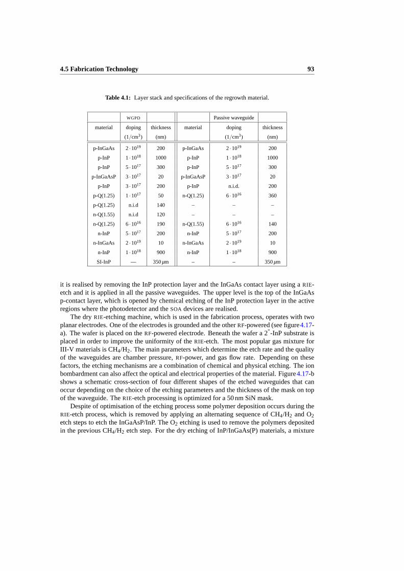
4.5 Fabrication Technology 93
Table 4.1: Layer stack and specifications of the regrowth material.
WGPD Passive waveguide
material doping thickness material doping thickness
(1/cm3) (nm) (1/cm3) (nm)
p-InGaAs 2·1019 200 p-InGaAs 2·1019 200
p-InP 1·1018 1000 p-InP 1·1018 1000
p-InP 5·1017 300 p-InP 5·1017 300
p-InGaAsP 3·1017 20 p-InGaAsP 3·1017 20
p-InP 3·1017 200 p-InP n.i.d. 200
p-Q(1.25) 1·1017 50 n-Q(1.25) 6·1016 360
p-Q(1.25) n.i.d 140 – – –
n-Q(1.55) n.i.d 120 – – –
n-Q(1.25) 6·1016 190 n-Q(1.55) 6·1016 140
n-InP 5·1017 200 n-InP 5·1017 200
n-InGaAs 2·1019 10 n-InGaAs 2·1019 10
n-InP 1·1018 900 n-InP 1·1018 900
SI-InP — 350µm – – 350µm
it is realised by removing the InP protection layer and the InGaAs contact layer using aRIE-etch and it is applied in all the passive waveguides. The upper level is the top of the InGaAsp-contact layer, which is opened by chemical etching of the InP protection layer in the activeregions where the photodetector and theSOA devices are realised.
The dryRIE-etching machine, which is used in the fabrication process, operates with twoplanar electrodes. One of the electrodes is grounded and the otherRF-powered (see figure4.17-a). The wafer is placed on theRF-powered electrode. Beneath the wafer a 2” -InP substrate isplaced in order to improve the uniformity of theRIE-etch. The most popular gas mixture forIII-V materials is CH4/H2. The main parameters which determine the etch rate and the qualityof the waveguides are chamber pressure,RF-power, and gas flow rate. Depending on thesefactors, the etching mechanisms are a combination of chemical and physical etching. The ionbombardment can also affect the optical and electrical properties of the material. Figure4.17-bshows a schematic cross-section of four different shapes of the etched waveguides that canoccur depending on the choice of the etching parameters and the thickness of the mask on topof the waveguide. TheRIE-etch processing is optimized for a 50 nm SiN mask.
Despite of optimisation of the etching process some polymer deposition occurs during theRIE-etch process, which is removed by applying an alternating sequence of CH4/H2 and O2
etch steps to etch the InGaAsP/InP. The O2 etching is used to remove the polymers depositedin the previous CH4/H2 etch step. For the dry etching of InP/InGaAs(P) materials, a mixture

94 4. Waveguide pin-photodetector
S I - I n PB u f f e r
g u i d e
C l a d
S h a l l o w W GD e e p W G S O AP D
S u b s t r a t e l e v e l
D e e p l e v e l
S h a l l o w l e v e l
Figure 4.16: Structure of all of components (photodetector:PD, deep waveguide,SOA, andshallow waveguide) after the finalRIE-etch .
R F - p o w e rS u b s t r a t ec h i p
P l a s m a
(a) (b)
Figure 4.17: (a) Dry RIE-etch machine configuration. (b) schematic cross-section of fourtypesRIE-etched ridge with the mask on top.
of CH4/H2 (100/80SSCM) gases is applied at a chamber pressure of 60 mTorr with 200 WRF-power at a frequency of 13.56MHz.
After each 120 seconds of CH4/H2 etch, a 12 seconds O2 etch at a pressure of 100 mTorrand anRF-power of 200 W is applied to remove the deposited polymer.
The measured etch rates for InP/InGaAsP/InGaAs are about 55/33/25 nm/minute, respec-tively. The etch rate depends on the material composition, the doping level, and the ratio ofthe masked to non-masked surface regions. Therefore, in order to achieve accurate control theetch depth has to be measured during the etching process.
4.5.3 Passivation and planarization with polyimide
An essential requirement for a receiver is a low dark current. Therefore, the photodetectorsand SOAs should be passivated in order to avoid degradation of the device performance. Inthe receivers based on the twin-guide scheme, we found that passivated photodetectors with

4.5 Fabrication Technology 95
a 350 nm SiN passivation layer showed a dark current of less than 10 nA at a 5 V reversebias voltage. In order to be compatible with the active-passive integration process as it isused for other devices, we decided to apply polyimide (PI-2737) for passivation of the presentMWR. Polyimide exhibits a good thermal and mechanical stability (>300C), and it has a goodchemical resistance.It has a refractive index of 1.62 at 1.55µm wavelength. The procedureconsists of two series of steps, one for passivation and one for planarisation. The latter isnecessary to make the surface sufficiently flat to be able to open the polyimide selectivelyabove the p-contacts, while keeping it closed above the waveguides where the contact layerhas been removed.
For passivation, a layer of polyimide was spun at a speed of 6000RPM, and a pre-bake serieswas applied at temperatures of 100, 150, and 200C for about 5, 5, and 10 min., respectively, onin-line hot plates. After spinning a second polyimide layer, the procedure with the hot plateswas repeated and a final curing step in a convection oven under Nitrogen gas was applied.The polyimide was cured for an hour at 300C,which is the maximum temperature of theoven. Curing of the polyimide occurs by removal of the solvents or other volatiles and also byimidization of the polyimide. It leads to hardening of the material. For optimal adhesion of thepolyimide to the semiconductor material, an adhesion promoter (VM -653) is spun at a speed of2000RPM prior to the spinning of the first layer of the polyimide.
After this passivation step another series of polyimide deposition steps is applied in orderto planarise the surface sufficiently for selective opening of the metal contacts. For effectiveplanarisation of the deep regions, a layer of the polyimide was spun and prebaked at a tem-perature of 100C for 3 min. Then the polyimide was exposed by a negative substrate mask(i.e. the mask used for definition of the substrate level) and the exposed parts were removedby developing and rinsing in PyralinDE-9040 and Butyl acetate for 30 sec, respectively. Thisstep was repeated several times until the surface was sufficiently flat. The deep parts were alsocovered in a similar way by using a negative deep mask.
Every time after spinning and curing of two layers, the height profile was measured with aTencor profiler. The polyimide layers have to be spun and cured several times until the heightdifferences of the polyimide in the different points of the wafer are less than the thickness of theInGaAs contact layer and protection layer to avoid that the passive waveguide will be openedand metalised too. We applied 14 layers in order to achieve a sufficiently planar surface. Sincethe temperature of annealing is at 325C, a final curing is done in a programmable oven from200 to 325C in steps of 25C with a duration of 5min for each step.
After coating the wafer with polyimide, we need to open the p-contact of the photodetectorsand theSOA. Polyimide can be isotropically etched in the barrel etcher by a gas mixture ofO2 / CF4. The etch rate depends on the pressure of the gas composition andRF-power. Agas composition of 5SSCMCF4 and 45SSCMOxygen under a power of 300 Watt yields a fastetch-rate of 300 nm/min and a composition of 15SSCM Freon and 35SSCM O2 yields a slowetch-rate of 50 nm/min (see figure4.18-a).
Dry etch-back of the polyimide is also possible in aRIE-etch machine. Experimentsshowed that with a gas mixture of 20SSCMO2 and 2SSCMCHF3, under a 50 WattRF-powerand a 15mTorr pressure, an etch rate of 100nm/min was achieved. The dryRIE-etch is suitablefor opening the polyimide on the lateral n-contact regions with a Ti or Au mask. The gas mix-

96 4. Waveguide pin-photodetector
(a) (b)
Figure 4.18: (a) Etch back after polyimide spinning. (b)A photograph of the seed layerwhich is deposited by a sputtering machine.
ture attacks the Ti, therefore the thickness of Ti has to be sufficient, to leave sufficient materialfor the contact. This depends on the thickness of the polyimide layer that has to be opened.The gold is not attacked by the etch.
4.5.4 Metalization
The metalization of theMWR chip is accomplished with a combination of evaporation andsputtering. The main drawback of the evaporation technique is that it cannot cover sidewallswhereas in the photodetector, we require to make interconnections over height steps betweenthe p- and n-contact metalization and probe-pads. Sputtering, on the other hand, has a goodcoverage of the sidewalls but, as a result, it is not suitable for lift-off. For both evaporation andsputtering deposition of thick gold layers on the wafer is costly. Therefore, a third technique,electro-plating, is used for selective deposition of thick gold layers. Electroplating of goldrequires a seed layer on all surfaces of the wafer where the gold has to be deposited. This seedlayer is deposited in the sputtering machine as depicted in figure4.18-right. In conclusion, acombination of three methods is used to deposit the contacts and a thick layer of gold.
The metal layer stack for the p- & n-contact consists of three layers: 25 nm Ti, 75 nm Pt,and 300nm Au. The deposition has been done using an e-gun evaporation machine. To obtaina low contact resistance the metalization has been annealed in a rapid thermal annealer, in anitrogen gas atmosphere at 325C for 60 sec.
High frequency devices such as photodetectors and modulators require a thick electrode toobtain a lowRF-loss. Calculations shows that a gold layer with a thickness of at least 1.5µmhas a sufficiently lowRF-attenuation [42].
Two types of electroplating are 1)a constant current mode (galvanostatic) and 2) a constantvoltage mode (potentiostatic) [94, 95]. In the figure4.20-b, the curve of current vs. potentialwith a rotating electrode is depicted. In the galvanostatic technique, the current is controlled

4.5 Fabrication Technology 97
P u l s eg e n e r a t o r p o t e n t i o s t a t e 2
e 1
e 3i ( t )
i ( t ) m e a s u r e d w a t e r ( 5 0 d e g )
i n
o u t
m a g n e t i c s t i r r e r
P l a t i n i z e dt i t a n i u m g r i d
s a m p l e c l a m p
w o r k i n g e l e c t r o d e
r e f e r e n c ee l e c t r o d e
c o u n t e re l e c t r o d e
(a) (b)
Figure 4.19: (a) Schematic diagram for the potentiostatic technique. e1, e2, e3 are working,reference, and counter electrodes, respectively. (b) Gold plating setup.
and the voltage is measured. The drawback of this technique is that the current density changesduring the electroplating, which results in a change of the working point from the crystalliza-tion regime to a regime in which the quality of the layers is degraded by gas formation or to aregime with a very low deposition rate.
To solve this problem, a potentiostatic technique is used. In this technique the voltageis kept constant and the current is measured. A schematic view of the electro-plating setupis depicted in figure4.19-a. The potential of the working electrode, e1, is controlled by thepotentiostat with respect to the reference electrode e2 and the current i(t) is measured duringthe electroplating. A pulsed voltage is applied between the work and reference electrodes [96].In figure4.20-a, the measured current response is shown while the pulse voltage is oscillatingbetween -0.575 V (for a 5 sec.) and -0.4 V (for 30 sec.). Both values are in the working region.
Using a pulsed voltage instead of a constant voltage has several advantages: preventingH2 gas formation by applying a special voltage, less surface roughness, and small grain size.In figure4.19-right, the plating setup is demonstrated. The bath contains an ammonium goldsulphide solution and has to be maintained at a constant temperature of 50C. A pH-meter isalso used to check the characteristics of the bath solution prior to the start of the electroplating.It should have a pH of 9.5.
4.5.5 Processing scheme
In figure4.21 the various processing steps for the fabrication of the integrated active-passivewaveguide devices are illustrated. The paragraph labels correspond to the numbers of thefigures.

98 4. Waveguide pin-photodetector
0 10 20 30−0.06
−0.04
−0.02
0
0.02
time (s)
i(t)
(mA
)
−1 −0.5 0−0.3
−0.2
−0.1
0
0.1
working electrode voltage (V)
Cur
rent
(m
A)
working point
low deposition
gas formation
(a) (b)
Figure 4.20: (a) Variation of the current of the working electrode vs. time during theelectroplating. (b) Potential-current curve of the working electrode at a typical rotationspeed. Three regimes of the working points, gas formation and low-deposition are indicatedon the curve.
A. Definition of the passive and active regions:A 85 nm thick SiN mask is deposited in aPECVD machine. This thickness is sufficient to the shallow, deep, and substrate regions2.7µm deep using aRIE-etch. TheRIE-machine recipe was also optimized for an 80 nmthick SiN mask layer. Next the passive waveguide, photodetector andSOA ridge patternswere defined in the SiN with positive resist (HPR 504) and vacuum contact lithographyusing a Karl Suss MA6 mask aligner.
B. Substrate etch:A layer of negative resist (MAN 440) is spun on top of the SiN mask layer.The substrate pattern is defined in the photoresist by using a negative (dark) mask. Next,a 100nm Ti layer, which serves as a protection mask for the first etch step, is evaporatedon top of the photoresist. The processing is followed by the lift-off of the photoresist inacetone and isopropanol for about 30 minutes. In the first step of theRIE-etch, 1.25µmis etched.
C. Deep etch: In step 2 the Ti-layer is dissolved in a solution of 4 gram oxalic acid, 25 mlKOH (4M), and 50 ml H2O2 (30%) for about 210” . Another Ti mask is used to definedeep parts by using a negative photoresist, Ti evaporation, and a lift-off. Subsequently,the secondRIE-etch step is employed in which the height is about 370 nm for deep partand 1840 nm for substrate parts.
D. The first waveguide etch:After removal of the Ti, the thirdRIE-etch step is carried out byusing the SiN mask layer. The etch depths for the shallow, deep and substrate regionsafter this step are about 1200, 1800, 3000 nm, respectively.

4.5 Fabrication Technology 99
A
S I - I n P
n + - I n P n + - I n G a A sn - I n PQ ( 1 . 2 5 )
Q ( 1 . 5 5 )g r a d e d p - I n Pp + - I n G a A sI n P
S i NT i
B
C D
E
P R
F
G
P o l y i m i d e T i
H
Figure 4.21: Processing scheme that is used in the fabrication of theMWR on SI-InP.

100 4. Waveguide pin-photodetector
K
P R T i / P t / A u
L
M
S e e d l a y e r ( A u )
P l a t i n g ( A u )
N
O P
Figure 4.22: Processing scheme that is used in the fabrication ofMWR on SI-InP (contin-ued).

4.5 Fabrication Technology 101
E. Removing the SiN from the passive waveguides:By using the mask for the active regiondefinition which is used in the first epitaxial regrowth step, in combination with a posi-tive photoresist, all the non-active regions are exposed. Next, SiN is removed from thepassive waveguides by a buffered HF solution.
F. The second waveguideRIE -etch: After removal of the photoresist, all waveguides areRIE-etched. In this step, the InP protection layer and the InGaAs contact layer are etchedaway from the top of the passive waveguides. The shallow, deep, and substrate regionsare alsoRIE-etched 50 nm in the guiding layer, 100 nm through guiding layer, and morethan 200 nm in theSI-InP substrate, respectively.
G. Planarization and passivation:According to the previous description, a number of poly-imide layers are spun on the wafer and etched back after each step in order to arrive ata planarised surface. After this procedure the polyimide is etched backed in the barreletcher to open the p-contacts of theSOA and the photodetector.
H. The n-contact opening: The n-contact openings for theSOA and the photodetector aredefined in a negative photoresist (MaN 440) after which Ti is evaporated. After lift-off,the polyimide is etched away on the n-contact regions by using theRIE-etch machine.
K. Removal of the InP protection layer: By etching-back of the polyimide on the p- and n-contact regions, the InP protection layer and the n-InP buffer layer are chemically etchedaway with a solution of HCL:H3PO4 to ensure that the p- and n-contact metalization areon the p- and n-InGaAs contact layer, respectively.
L. Contact metalization: The metalization pattern of the p- and n-contacts is defined innegative photoresist. The contact layers Ti/Pt/Au (25/75/300 nm) are evaporated (seefigure4.23). The Ti layer is utilized to make a low electrical contact in connection withthe underlying InGaAs p- and n-contact layers. The Pt is a barrier material to preventinterdiffiusion of Au into the InGaAs layer during the annealing step after the contactmetalization.
M. Seed layer: A 100 nm Au was sputtered on the surface of the chip to ensure that thesidewalls and the surface of the chip are covered with a thin layer of gold. Figure4.18-right shows aSEM picture of the seed layer on the sidewall and surface of the chip.
N. & O. & P. Electro-plating: A thick layer of photoresist (AZ 4533) is spun on top of thechip. A mask which defines the patterns of the p- and n-contacts and the probe pads oftheSOA and the photodetectors is utilized for exposing the photoresist. Next, a layer ofgold with a thickness of more than 1.5µm is electroplated through the openings in thephotoresist. The photoresist is dissolved in the AZ-developer after a floating exposure.The seed layer is removed in Degussa Entgoldungslosung 645 solution. After removingthe seed layer, some tracks of the plated gold can be observed which can make a shortcircuit between two devices. In figure4.24, the gold-plated signal and ground electrodeson theSOA (left) and the photodetector (right) are shown. Finally, by using the SiNRIE

102 4. Waveguide pin-photodetector
n - c o n t a c t n - c o n t a c t
p - c o n t a c t
p a s s i v e w a v e g u i d e
Figure 4.23: Ti/Pt/Au evaporated pattern for the photodetector with a 2µm wide p-mesa.
n - c o n t a c t
p - c o n t a c t
p - c o n t a c t
n - c o n t a c t
n - c o n t a c t
Figure 4.24: The electrode pads of (left) theSOA and (right) the photodetector after plating.
machine, the polyimide is removed from the chip except beneath the gold-plated regions.
4.6 Characterization
Several static andRF-measurements are carried out on theWGPDs. The static measurementsinclude dark current and responsivity of the photodetectors at different bias voltages and wave-lengths. TheRF-measurements are carried out to determine the output reflection coefficient(S22) andRF-responsivity, including the 3-dB bandwidth of the photodetectors.

4.6 Characterization 103
−4 −3 −2 −1 0−20
−15
−10
−5
0
5
10
15
Bias voltage (V)
Dar
k cu
rren
t (nA
)
40µm
60µm
500µm1000µm
Figure 4.25: Dark I-V curves for several photodetectors.
4.6.1 static measurements
The measurement setup for the static measurement is the same as the setups used for the char-acterization of the twin-WGPDs. The dark current vs. biasing voltage swept from -4V to 0.5Vis shown in figure4.25for 40, 60, 500, and 1000µm long devices. It shows that the dark cur-rent is less than 20 nA at voltages smaller than –4 volts which demonstrates a reasonable darkcurrent for the devices which are passivated with polyimide. The longer devices show moredark current at higher bias voltages.
4.6.2 Responsivity and efficiency
The static responsivity of the photodetectors has been determined by launching an opticalpower of -10 dBm from a tunable laser into the detector chip, applying a bias voltage andmeasuring the detector current via two needles on the p- and n-electrode of theWGPD usinga Keithly current meter. The wavelength of the tunable laser has been swept from 1440 to1600 nm. By accounting for the optical fiber and connector losses of 0.5 dB, a fiber-chip cou-pling loss of 4dB and a passive waveguide loss of 2dB, the responsivities of the photodetectorshave been determined. The internal responsivity of a 70µm longWGPD is shown in figure4.26at bias voltages of –1, –5, and –10 V. The output power of the tunable laser is constant dur-ing measurement while changing the wavelength. The internal responsivity decreases beyondthe bandgap wavelength of the absorbing (Q1.55) layer as we determined in figure4.4-b. Byapplying a larger reverse voltage across the depletion layer, the depletion layer broadens andmore photons are absorbed which results in a higher responsivity.
We expect that the efficiencies exponentially increase with increasing length of the pho-todetectors (see figure4.4-a). However, because of the non-uniformity of the wafer and theprocessing the photodetectors are not similar, and the efficiencies do not increase exponen-

104 4. Waveguide pin-photodetector
1450 1500 1550 16000
0.2
0.4
0.6
0.8
Wavelength (nm)
Res
pons
ivity
(A
/W)
−1V
−5V
−10V
Figure 4.26: Internal responsivity as a function of wavelength for a 70µm long photode-tector at bias voltages of –10, –5, and –1 volts.
tially with increasing device length. The internal efficiency is also determined for a 70µmlong device at two biasing voltages of –5 and –10 V which show a more than 5% increase ofthe efficiency due to broadening of the depletion layer. Figure4.26shows that the absorptionlayer is not fully depleted at –5 V. From the figure4.26two effects are visible: with increasingbias voltage the absorption increases, and the band edge shifts to longer wavelengths. The firsteffect can be explained by widening of the depletion layer, the second by the Franz-Keldysheffect.
4.6.3 RF-measurements
Electrical and optical/electrical measurements have been carried out to evaluate the photode-tectors. A 20 GHz lightwave component analyzer has been used to measure the frequencyresponse and the output reflection coefficient of theWGPDs.
output reflection coefficient (S22)
The output reflection coefficients of several photodetectors have been measured at a bias volt-age of−5V by a 20GHz lightwave component analyzer as shown in figure4.27-a. The resultshave been obtained by de-embedding the measurement setup for the effects of theRF-cables,the bias-tee and theRF-probe. The measured output reflection coefficients (|S22|) for the pho-todetectors with 70, 110, 400, and 900µm long show that for the short devices (70 and 110µm)the 3-dB of the|S22| is well above 20GHz and for the long devices (400 and 900µm) the 3-dBof |S22| is below 20 GHz.
RF-responsivity
TheRF-responsivity of several photodetectors has been obtained by coupling light from a tun-able laser to theWGPDs and measuring theRF-signal using anRF-probe, bias-tee,RF-cables

4.7 Conclusions 105
0 5 10 15 20−6
−5
−4
−3
−2
−1
0
Frequency (GHz)
Out
put r
efle
ctio
n (d
B)
900µm
400µm
110µm
70µm
0 10 20 30 40 50 60 70−34
−32
−30
−28
−26
−24
−22
Frequency (GHz)
RF
−R
espo
nsiv
ity (
dB)
−4V
−8 V
(a) (b)
Figure 4.27: (a)output reflection coefficient vs. frequency for several photodetectors at−5 V bias voltage. (b)RF-Responsivity vs. frequency for 60µm long photodetectors at biasvoltage−4 and−8 V and 1.5µm wavelength.
and 67 GHz lightwave component analyzer. The bias voltage is set to−4 and−8 V and thewavelength is set to 1.5µm. The measuredRF-signals are shown in figure4.27-b. It shows abandwidth of about 30 GHz at−4 and−8 V bias voltages which is in agreement with the out-put reflection coefficient measurement. So, it confirms that theRC-bandwidth is dominant. Byincreasing the bias voltage the depletion layer thickness increases and more photons contributeto the photocurrent, while at the same time the junction capacitance decreases so that the 3-dBbandwidth increases. TheRF-responsivities show resonances with a period of 3.3 GHz whichresult from a mismatch between photodetector and probe that was not completely removed bythe calibration.
4.7 Conclusions
To design a high-speedWGPD with a high-quantum efficiency that can be monolithically in-tegrated with passive waveguide devices andSOAs, we require a compromise between thespecifications of theWGPD and the passive waveguide. The effects of the width, length, andactive layer thickness on the internal quantum efficiency have been investigated, from which itappears that the internal quantum efficiency is mainly determined by the length of the detector.Once the length is fixed the width has to be chosen as small as possible in order to reducethe capacitance of the detector and make the RC-limited bandwidth as large as possible. Thecapacitance can be further reduced by increasing the depletion layer thickness, but this willcause the transit time to increase. Here a compromise has to be made, which is dependent onthe chosen detector length.

106 4. Waveguide pin-photodetector
It is demonstrated that with a graded doping level and choosing a suitable thickness for thecladding and buffer layers, a good trade-off between the electrical resistance in theWGPD andoptical loss in the passive waveguide is possible.
Based on calculations, it is determined that with a 100µm long and 2µm wide p-mesa,and 500 nm etch depth of theWGPD, 90% quantum efficiency and 42 GHz bandwidth areachievable. Further, it is shown that with a graded doping level and a proper thickness for thecladding layers, the additional optical loss of the passive waveguide as a result of the dopingof the top cladding layer can be restricted to about 3.5 dB/cm.
The maximum bandwidth is found as an optimum between a small drift time (thin depletionlayer) and a small capacitance (thick depletion layer). From Figure4.10 it is seen that for adetector with 10µm length and 2µm width the optimum is around 60 GHz. By reducing thedetector width to 1µm, this could be increased to around 100 GHz. This requires a moredifficult technology, however. A further increase can be achieved by applying a TravelingWave detector design, in which the speed of the lightwave is matched to that of theRF wave.Using this approach the Heinrich Hertz Institute has reported bandwidths up to 110GHz. Thisis about the limit of the present approach.
SeveralWGPDs have been characterized to evaluate the dark current, efficiency and 3-dB bandwidth. The measurement results demonstrate a very low dark current (about 15 nAat –4 bias voltage) and more than 65% internal efficiency for a 60µm long device at –5 Vbias voltage and 1.5µm wavelength. The output reflection coefficient andRF-responsivitymeasurements show a 30GHz bandwidth for a 60µm long device.

Chapter 5
Design of a pre-amplified MWR onSI-InP
In this chapter design and preliminary experimental results on the development of a multi-wavelength receiver (MWR) with an integrated optical pre-amplifier on a semi-insulating sub-strate are presented. The semi-insulating substrate is required for improvedRF-performance.The receiver chip consists of a semiconductor optical amplifier (SOA), an AWG-demultiplexerand an array of waveguide-photodetectors (WGPDs). The use of a semi-insulating substraterequired development of lateral n-contacts. Experimental results are reported in this chapter.
5.1 Introduction
Integration of a pre-amplifierSOA in a MWR brings a number of advantages for applicationin optical communication networks. Losses associated with coupling from fiber to chip andon-wafer losses are compensated, the optical sensitivity can be enhanced and the number ofpackaging steps is reduced.
In this chapter, we report design and some characteristics of the first high-speedMWR witha monolithically integrated pre-amplifierSOA, anAWG and an array of eight pin-photodetectorson SI-InP substrate. Until recently this device was the first high-speedWDM receiver with anintegratedSOA preamplifier. The semi-insulating substrate enhances the dynamic performanceof the receiver. First we discuss the concept of the pre-amplifiedMWR. Next the main featuresof a SOA including optical power gain and gain saturation and effects of facet reflection on gainare investigated. The dynamic performance of theMWR is characterized by the bit-error-rate(BER) and the sensitivity of the receiver which is determined by the noise contributions of thedifferent components (section5.4). It is shown that using a pre-amplifierSOA, the sensitivity
107

108 5. Design of a pre-amplified MWR on SI-InP
can be enhanced substantially when theSOA has sufficient gain and theAWG has a sufficientlylow crosstalk.
In section5.5we discuss the basic components of the pre-amplified receiver: the semicon-ductor optical amplifier, the compactAWG demultiplexer, the multi-mode interference modefilter, the passive waveguides, adiabatic tapers and shallow-deep transitions. Finally, in section5.6some experimental results on lateral side contacts, necessary for high-speed operation, aredescribed.
Steenbergenet al.[34, 48, 97] reported a twin-guideMWR consisting of anAWG and fourphotodetectors. The bit-error-rate (BER), measured with and withoutEDFA pre-amplifier at1.2 Gb/s for aPRBSof 27–1 showed an increase of 25 dB sensitivity by using anEDFA. A WDM
receiver composed of aSOA, an AWG demultiplexer, and a photodetector-array was reportedby Zirngible et al.[98]. They showed that a sensitivity better than –31 dBm at 5 Gb/s isattainable. Kikuchi [99] described a 64-channelWDM wavelength-selective receiver including64 SOAs, two AWGs, and a photodetector with−14 dBm sensitivity at 10−9 BER for an NRZ
signal at 1.25 Gb/s. A transmitter/receiver with a capacity 40 Gb/s per channel (aggregate datarate of 400 Gb/s with 10 channels) has been commercially applied [39]. The receiver includesan AWG and an array of 10 photodetectors which show a 26 GHz bandwidth adequate for a40 Gb/s capacity of the individualWDM channels.This device did not include a preamplifierSOA. The active layer in the transmitter and the receiver are bulk and quantum well materials,respectively. Recently, Infinera has reported a receiver including aSOA, AWG and an array ofphotodetectors for 40 channel operating at 40 Gb/s [40, 43]. In this chapter we will discuss thedesign and some experimental results on the development of a 4 channel MWR with 40 Gb/schannel capacity and an integrated pre-amplifier.
5.2 Concept of the pre-amplified MWR
Figure5.1 shows a schematic view of the pre-amplifiedMWR which consists of aSOA, aneight-channel polarization independentAWG, and eight photodetectors. In this schematic amodulated optical signal is launched via the input port (1) to the pre-amplifierSOA. Theamplified signal, includingSOA noise enters into theAWG to separate the received wavelengthsand to suppress the out-of-bandSOA noise. The separated wavelengths are then transformedto an electrical signal in the detectors. By using input port 2 we can characterise the receiverwithout theSOA. With this configuration, we can easily investigate the performance of theMWR with and withoutSOA. It is also possible to compare the performance of theMWR usinganEDFA instead of theSOA.
5.3 Semiconductor optical amplifiers
After the advent of optical amplifiers, the use of all-optical (O/O) networks is increasing. Insuch networks the number of conversions of the signal from the optical to the electrical domain(O/E) and vice versa is strongly reduced. Further optical amplifiers reduce the relative contri-

5.3 Semiconductor optical amplifiers 109
S O A AWG
P D
P D
P D
l 1 . . . l 8
l 1
l 2
l 8
l 1 . . . l 8
S O A AWG
P D
P D
P D
l 1 . . . l 8
l 1
l 2
l 8
l 1 . . . l 8
i n p u t ( 1 )
i n p u t ( 2 )
Figure 5.1: A schematic view of an eight-channelMWR.
bution of the electrical noise generated by the photodetector and the electrical pre-amplifier.An optical amplifier itself adds some noise, however, which is discussed in section5.4.3.
Optical amplifiers play an important role in the development and the expansion ofWDM
networks. The three main applications of the amplifiers in such networks are as transmitterbooster amplifier, linear optical repeater, and receiver pre-amplifier. In aMWR, the SOA op-erates as an optical pre-amplifier to compensate the coupling loss and on-wafer optical lossesoccurring in the passive integrated circuit.
In a SOA, a number of parameters and effects have to be studied. The main ones are opticalpower gain and gain saturation, the effect of facet reflection on gain, and the noise behavior.The last one will be discussed later in section5.4.
Optical power gain and gain saturation
For aSOA with an input optical signalPin = P0 the amplified signal at the output, for a biascurrentIb, can be described as:
Pout = GsPin +Pn (5.1)
whereGs = PoutPin
|λ=λ0is the ideal single-pass gain of theSOA (without noise) andPn is the
optical noise added by theSOA. The equation that describes the propagation of the opticalpower through theSOA is:
dP(z)dz
= g(z)P(z) (5.2)
wherez is the position (z= 0 is the input facet of theSOA) in the direction of the light propa-gation andg(z) is the gain at positionz, defined as:
g(z) =g0
1+ P(z)Psat
(5.3)

110 5. Design of a pre-amplified MWR on SI-InP
wherePsat denotes the saturation power, i.e. the power where the gain is reduced with 3 dB,andg0 is the gain at low input power. By substituting eq.5.3 in eq.5.2, the single pass gaincan be determined as:
Gs = eR l0 g(z)dz (5.4)
If we assume a uniform gain profile for theSOA (g(z) = g), which is attainable at low inputpowers (no saturation) by uniform injection of the bias current into the active layer,Gs =exp(gl). The optical gaing follows from the material gain of the active layergm, the fractionΓ of the confined power in the active layer, and the total internal lossαs of theSOA, as:
g = Γgm−αs (5.5)
The material gaingm depends on the bias currentIb and has a wavelength dependence that canbe approximated by a parabolic curve with a peak gain of
gm = a(N−N0) (5.6)
wherea is a gain constant,N is the carrier density, andN0 is the transparency density. At lowsignal levels and neglecting any non-radiative contributions from the bias current, the carrierdensity is related to the bias current as
N =IbτeV
(5.7)
whereV is the volume of the active layer,e is the electron charge andτ is the recombinationtime constant. The relation between bias current and photon emission may be approximatedby the steady state rate equation:
IbeV
=Nτ
+ΓgmP
hν(5.8)
wherehν is the photon energy andP is the optical power. This relation describes a balancebetween injected carriers (Ib
eV), the spontaneous emission (Nτ ) and the stimulated emission
( ΓgmPhν ).The saturation output power (see eq.5.3), at which the gain of theSOA has fallen by 3 dB
from its unsaturated value, is given by the relation:
Psat=dwhν ln2
Γτa(5.9)
whered is the active layer thickness andw is theSOA width.TheSOA gain may show polarization dependence due to the difference in the confinement
factor Γ for the TE and TM polarizations because the active layer is not symmetrical withrespect to the transverse dimensionsx andy.

5.4 Sensitivity of the MWR 111
0 10 20 30−100
−80
−60
−40
−20
0
Angle (deg)
Ref
lect
ivity
(dB
)
TE
TM
Figure 5.2: Calculated reflectivity as a function of the waveguide facet angle for a 3µmwide waveguide. At an angle of 11.5 degrees the reflectivity is reduced below10−5.
Effects of the facets reflection on gain
One of the principal problems for aSOA is the reflection at the facets, which will cause ripple inthe spectral transmission curve. In the literature, three methods for suppressing the reflectionsare utilized:AR-coating, angled input and output waveguides, and a window facet structure.
The most popular method to achieve low facet reflectivity is by usingAR-coatings. Re-flectivities as low as 10−4 can be achieved with high-qualityAR-coatings. Another methodis to apply a window facet structure, a non-guiding diffraction region between theSOA andthe cleaved-end facet. With this method a reflectivity in the order of 10−4 is reported [100].Combination of the two will reduce the reflectivity further.
In figure5.2 the dependence of the reflectivity of a tilted input/output waveguide on thetilting angle [87, 101–103] is shown. It is seen that with a tilted passive waveguide with awidth of 3 µm and an angle of 11.5 degrees, a reflection in the order of 10−5 is predicted.It is extremely sensitive to the facet angle, however, and can only be realised in a narrowwavelength window.
The reflection at the facet of theSOA creates a gain ripple due to Fabry-Perot resonances.The gain ripple of theSOA is determined as:
r i = 20log
(1+G
√R1R2
)(1−G
√R1R2
) (5.10)
With a gain of 20dB and a gain ripple below 0.1dB the reflectivity should be kept below10−4.
5.4 Sensitivity of the MWR
In a receiver, photons are converted to electron-hole pairs, that generate an electrical signal. Inthis process, the optical signal will be distorted by unwanted noise, so that the receiver perfor-

112 5. Design of a pre-amplified MWR on SI-InP
S O AG , h i n
O p t i c a l f i l t e rh o u t
P sn , l P D
hE l e c t r i c a l A m p l i f i e rB e , R L
S O AG , h i n
O p t i c a l f i l t e rh o u t
P sn , l P D
hE l e c t r i c a l A m p l i f i e rB e , R L
Figure 5.3: (left) A front-end receiver consisting of a pin-photodetector and an electri-cal amplifier. (right) An optically pre-amplified receiver with an optical passband filter tosuppress the noise.
mance is limited by the noise characteristics. In order to enhance the receiver performance itis important to know the noise contribution of the different receiver components.
In this section, we describe the noise and sensitivity in two types of receiver that are shownin figure 5.3. In the front-end receiver, consisting of a pin-photodetector and an electricalpost-amplifier (see figure5.3-left), an input optical signalPs couples to the photodetector witha quantum efficiencyη. The generated photocurrent is then amplified in the electrical post-amplifier. The bandwidth and input impedance of the electrical amplifier are denoted asBe
andRL(= 50Ω), respectively.In the optically pre-amplified receiver, indicated in figure5.3-right, the optical signalPs
is first amplified in theSOA. The noise added by theSOA is filtered when it passes throughthe optical filter. The photodetector detects both the signal and the residual noise power. Infigure5.4, the signal and noise power level at different positions in an optically pre-amplifiedreceiver are schematically shown.
In subsection5.4.1the noise in the different components of a receiver is described and insubsection5.4.5the receiver sensitivities for the two types of the receiver are then determined.TheSOA and photodetector parameters that are used in this section are listed in table5.1. Basedon these parameters, a discussion on the sensitivity enhancement in the optically pre-amplifiedreceiver is given.
5.4.1 Receiver noise
The noise sources in a receiver can be classified roughly into two categories [104]: the first isoriginating from the intrinsic physical effects in theSOA and the photodetector, e.g. thermalnoise and shot noise. The other comes from the interaction between the different signal andnoise components, such as beating between the signal and the amplified spontaneous emission(ASE) noise.
The characteristics of some noise distributions depend on the signal: when the opticalsignal is zero, the noise disappears. This is for example the case for the beating between theASE noise generated by theSOA and the optical signal in the photodetector. However, most

5.4 Sensitivity of the MWR 113
Signa
l or n
oise p
ower
S O A O p t i c a lf i l t e r
P h o t o d i o d e E l e c t r i c a la m p l i f i e r
P s
Gh i n h
A S E - n o i s e
Signa
l or n
oise p
ower
S O A O p t i c a lf i l t e r
P h o t o d i o d e E l e c t r i c a la m p l i f i e r
P s
Gh i n h
A S E - n o i s e
Figure 5.4: Signal and noise level in a pre-amplified receiver.
Table 5.1: Values of the used parameters in the sensitivity calculation of theMWR.
parameter description value
e electron charge 1.6 · 10−19 C
h Plank’s constant 6.63· 10−34 Js
k Boltzmann’s constant 1.38· 10−23 J/K
T temperature 300 k
Bo optical bandwidth 1.6 nm
Be electrical bandwidth 33 GHz
Ps input optical power –
λ wavelength 1.55µm
η quantum efficiency 100%
RL load resistance 50 ΩR total resistance 60 Ω
Idark dark current 10 nA
G SOA gain 20 dB
ν frequency 193.55 THz
ηin input loss 0 dB
ηout optical filter insertion loss 0 dB
nsp population inversion 2.5

114 5. Design of a pre-amplified MWR on SI-InP
of the intrinsic physical noise sources are independent of the optical signal. For example shotnoise due to the dark current and the thermal noise in the photodetector. The major noisedistributions in the receiver components are:
• SOA noise contributions: amplified spontaneous emission, spontaneous-signal (sp-sig)beating noise, and spontaneous-spontaneous (sp-sp) beating noise.
• Photodetector noise contributions: shot noise and thermal noise.
• AWG noise contribution: signal-crosstalk beat noise.
Each noise source creates a noise current component in the photodetector. In the followingsections we will first discuss the photodetector noise, and then theSOA andAWG noise contri-butions.
5.4.2 Photodetector shot and thermal noise
The shot noise in the photodetector is due to the random generation and recombination of thecarriers. This random fluctuation leads to a noise power
Nsh = 2e(Is+ Idark)Be (5.11)
whereIs = ηPse/(hν) is the DC-photocurrent,η is the quantum efficiency,e is the electroncharge,h is Plank’s constant,ν is the frequency,Idark is the dark current andBe is the electricalbandwidth of the photodetector and the electrical post-amplifier. The shot noise is proportionalto the photocurrent and the dark current and to the photodetector bandwidth.
All dissipative (resistive) elements in electronic devices generate thermal noise. It is causedby the thermal fluctuations of the carriers in the semiconductor. The noise-contributing ele-ments of a pin-photodetector are the dark current shunt resistance and the series resistance inthe p- and n-doped cladding layers. The thermal noise of a resistance is given by
Nth =4KTBe
R(5.12)
whereK is Boltzmann’s constant,T is the absolute temperature (K) andR can be replaced bythe resistive elements of the load and the pin-photodetector.
5.4.3 SOA noise
The noise in aSOA originates from spontaneous recombination of the electrons and holes inthe active layer. The photons emitted in this process can be amplified which leads to a furtherincrease of the spontaneous emission power of theSOA. The amplified spontaneous emissionpower of theSOA is given by [105, 106]:
Psp =hνBogmnspexp[(gm−αs)L]−1
(gm−αs)(5.13)
5.4 Sensitivity of the MWR 115
wheregm is the material gain coefficient,αs is the internal loss coefficient of the ampli-fier, L is the amplifier length,nsp = N/(N−N0) is the population-inversion parameter,N0 isthe transparency carrier density,N is the injected carrier density,Bo is the bandwidth of theoptical filter. By defining theSOA gain asG = exp(gm−αs)L and assuming thatgm αs,equation (5.13) can be simplified to the well-known expression:
Psp = hνBonsp(G−1) (5.14)
In the case thatgm = αs (i.e. G = 1), relation (5.13) reduces to:
Psp = hνBonspLαs (5.15)
For an optical amplifier we can define a figure of merit to describe the noise performance. Thedegradation of the signal-to-noise ratio (SNR) in a SOA due to theSOA noise can be describedby a noise figureF as [107]:
F =(S/N)i
(S/N)o≈
1+2ηnsp(G−1)G
(5.16)
where(S/N)i is the input signal-to-noise ratio,(S/N)o is the output signal-to-noise ratio, andη is the quantum efficiency of the photodetector. The generated photocurrent due toASE-noiseand signal are given by
isp = Feηoutη(G−1)Bo (5.17)
is =ηeGtotPs
hν(5.18)
whereGtot = Gηinηout is the total path gain.In the photodetector, there is noise from beating between the signal and theASE-noise
and from beating of theASE-noise with itself. This beating creates two photocurrent noisecomponents [108]:
Ns−sp = 2e2Fηinη2outη
2G(G−1)PsBe/(hν) (5.19)
Nsp−sp = 0.5F2e2η2outη
2(G−1)2(2Bo−Be)Be (5.20)
whereNs−sp is the signal-spontaneous beat noise andNsp−sp is the spontaneous-spontaneousbeat noise.
The noise contribution of aSOA caused by the signal photocurrent and theASE photocur-rent is given by
Nsh = 2e(is+ isp)Be (5.21)
The total equivalent noise of theSOA in the photodetector is the sum of all noise compo-nents:
NSOA = Ns−sp+Nsp−sp+Nsh (5.22)
The noise contributions of the photodetector and theSOA for a pre-amplified receiver asa function of input power for an optical filter with bandwidths of 1.6 nm and 50 nm are

116 5. Design of a pre-amplified MWR on SI-InP
−50 −40 −30 −20 −10 010
−25
10−20
10−15
10−10
Input power (dBm)
Spe
ctra
l den
sity
(A
2 /Hz)
Signal
nth
nsp−sp
ntotal
nsh
ns−sp
−50 −40 −30 −20 −10 010
−25
10−20
10−15
10−10
Input power (dBm)
Spe
ctra
l den
sity
(A
2 /Hz)
Signal
nth
nsp−sp
ntotal
nsh
ns−sp
Figure 5.5: Spectral power density of noise and signal as a function of input power for areceiver with an optical filter passband width of 1.6 nm (left) and 50 nm (right). Gain of theSOA is 25 dB.
shown in figure5.5. It can be seen that for an input power of more than−30 dBm, the signal-spontaneous beat noise is dominant and for a very low input power, the total noise is dominatedby the thermal noise (see figure5.5-left) and the sp-sp beat noise (see figure5.5-right). Fora receiver with a narrow passband optical filter (e.g. 1.6 nm bandwidth), the signal power ishigher than the total noise until−42 dBm and for a wideband filter (e.g. 50 nm bandwidth)the signal power exceeds the total noise for an input power greater than−35 dBm. This meansthat the signal-to-noise ratio of an optically pre-amplified receiver can be enhanced by using anarrow passband optical filter between theSOA and the photodetector.
5.4.4 AWG signal-crosstalk beat noise
We analyse the noise level for anAWG with one input andN output waveguides. A light beamwith wavelengthsλ1, ...,λN is separated by theAWG into N separate wavelengths. Since theAWG is not ideal, a small amount of the optical power in each wavelength appears at the otheroutput waveguides [109, 110].
We define the optical field consisting of the signal and the crosstalk in theithchannel as
Ei(t) = ∑j
√2Ei j sin(ωit +φi j (t)) (5.23)
The subscriptsi, j (i, j = 1 toN) denote the output waveguide and the channel number, respec-tively, Ei j andφi j are the amplitude and phase of thej th channel in theith output waveguide,andωi is the optical signal angular frequency. The optical power in channeli, Pi(t), corre-sponds to| Ei(t) |2, therefore the generated photocurrents due to signal and crosstalk in thephotodetectors in channeli are

5.4 Sensitivity of the MWR 117
Ii = ℜ
(E2
ii + ∑j=1, j 6=i
2Eii Ei j cos(φii (t)−φi j (t))
)
+ℜ
(∑
i, j=1(i> j,i 6= j)2Eii Ei j cos(φii (t)−φi j (t))+ ∑
j=1, j 6=i
E2i j
)(5.24)
Whereℜ is the responsivity of the photodetectors and the first and last terms are the generatedcurrents due to signal and crosstalk, respectively. The second term is signal-crosstalk beatnoise and the third term is crosstalk-crosstalk beat noise. The current corresponding to thethird and fourth terms can be neglected in comparison to the first and second term.
The noise power of each beat noise component is given by 2E2ii E
2i j . Therefore, the total
noise power of each channel is∑ j 2E2ii E
2i j . The relative noise intensity of each channel can be
determined as the crosstalk normalized to the signal power of the channel:
σ2RIN =
N
∑j=1, j 6=i
2E2ii E
2i j(
E2ii
)2 (5.25)
If we define the crosstalk as the ratio of the signal power to the crosstalk power for theworst channel,Rx = PX
Ps, and we assume that the noise is present only when a “1” is received
(P1 = Ps, P0 = 0), and that the error probabilitiespe(1) = pe(0) = 0.5, then theRIN of thesignal-crosstalk beat noise is
σ2RIN = Rx(N−1) (5.26)
From this equation it is seen that the relative intensity noise of each channel contains thecrosstalk components of the other channels in the desired channel.
5.4.5 Receiver sensitivity
The receiver sensitivity is the minimum amount of the optical signal power that is required toobtain a specific signal-to-noise ratio. It can be described by the so-called Q-factor. Assuminga Gaussian distribution for the noise it can be derived from the signal and the noise power inthe "0" and "1" as [108]
Q =√
S1−√
S0√N1 +
√N0
(5.27)
whereS1 and S0 are the electrical signal powers in the receiver for "1" and "0" (mark andspace in digital communication) andN1 andN0 are the total noise powers for "1" and "0" inthe receiver. In a digital system, if we assume that the probability for "0" and "1" is equal

118 5. Design of a pre-amplified MWR on SI-InP
(Pe(1) = Pe(0) = 0.5), then the probability of a bit error as a function of the Q-factor can beexpressed as:
BER≈ 1√2π
exp(−Q2
2 )Q
(5.28)
Three often used BER-levels are BER=10−9 (Q=6), BER=10−12 (Q=7.03), and BER=10−15
(Q=7.094). With increasing Q-factor, the quality of the links increases.
In the following paragraph, the receiver sensitivity will be determined for direct detectionof an intensity-modulated digital signal∗.
Sensitivity of an optically pre-amplified receiver
If we assume that the received optical power for the "0" state is zero (S0 = 0), we have [111,112]: √
S1−√
S0 = GtotPsηe/(2hv) (5.29)
The total noise in the two states (N1 andN0) is given as:
N1 = Nth +Ns−sp+Nsp−sp+Nsh1 (5.30)
N0 = Nth +Nsp−sp+Nsh0 (5.31)
whereNsh1 andNsh0 are the shot noise contributions in the two states "0" and "1":
Nsh1= 2e(Is+ Isp+ Idark)Be (5.32)
Nsh0= 2e(Isp+ Idark)Be (5.33)
whereIsp andIs are defined in relations (5.17) and (5.18).By substituting the relations (5.29),(5.30) and (5.31) in relation (5.27) and after simplify-
ing, the receiver sensitivity as a function ofQ can be derived as:
Ps = (hcλe
)Q
Nth
η2G2tot
+2e2F
ηGtotηin(G−1
G)BoBe+
e2F2
2η2in
(G−1
G)2(2Bo−Be)Bo
2
+(hcλe
)Q
eQBo
ηGtot
+(
hcλe
)Q
eQBeF(G−1Gηin
)
(5.34)
∗IM-DD; intensity modulated direct detection or OOK: On-Off keying.

5.4 Sensitivity of the MWR 119
Sensitivity of a front-end receiver without pre-amplifier
With a similar discussion for an optically pre-amplified receiver, the mathematical expressionsfor the noise and the signal power of a front-end receiver without pre-amplifier, as shown infigure5.3-left are given as [111]:
Nsh1= 2e(Is+ Idark)Be (5.35)
Nsh0= 2eIdarkBe (5.36)
√S1−
√S0 = Psηe/(hv) (5.37)
Again, if we substitute relations (5.35), (5.36) and (5.37) in relation (5.27), the receiversensitivity follows as:
Ps = hcQ(√
Nth +eQBe)/(ηλe) (5.38)
Numerical results
In figure5.6-left, the sensitivities of the front-end and the pre-amplified receiver as a functionof the SOA gain are shown. The front-end receiver sensitivity can be improved by decreasingthe dark current and increasing the quantum efficiency (see relations5.35, 5.36, and5.37).We also calculated the sensitivity of the pre-amplified receiver as a function of the amplifiergain. With increasingSOA gain, the sensitivity of the pre-amplified receiver is enhanced. Thereceiver sensitivity has a floor, however, at an input power of about –60 dBm, below whichthe receiver sensitivity can not be improved by increasing theSOA gain. The difference insensitivity between the two types of receiver (front-end and pre-amplified) is depicted in fig-ure5.6-right, showing the sensitivity enhancement by a pre-amplified receiver as compared toa simple front-end receiver.
In figure5.7-a the sensitivity enhancement for three bandwidth values of the optical filteris presented. By decreasing the optical bandwidth from 100 nm to 1.6 nm, about 4 dB sensi-tivity enhancement can be achieved. The receiver sensitivity dependence on the spontaneousemission parameternsp is shown in figure5.7-b. For aSOA with a low gain, the sensitivitydependence onnsp is weak because the receiver sensitivity is dominated by thermal noise.However, at high gain, the signal-spontaneous noise limits the receiver sensitivity. The idealvalue fornsp is 1 and the minimum value reported isnsp = 1.4 (NTT). In a receiver with a lowquantum efficiency of the photodetector the receiver sensitivity can also be strongly enhancedwith a pre-amplifier (see figure5.7-c). The effect of the bandwidth of the photodetector andthe electrical post-amplifier is presented in figure5.7-d, which shows a receiver sensitivitydifference increase about 2 dB, if the bandwidth is increased from 10 GHz to 35 GHz.
From these figures we conclude that the best way to enhance the receiver sensitivity is touse a narrow band optical filter after theSOA.

120 5. Design of a pre-amplified MWR on SI-InP
0 10 20 30 40−60
−55
−50
−45
Gain (dB)
Sen
sitiv
ity (
dBm
)
0 10 20 30 40−15
−10
−5
0
Gain (dB)
Diff
eren
ce s
ensi
tivity
(dB
)
Figure 5.6: (left) Sensitivity of simple front-end and pre-amplified receivers. (right) Differ-ence between the two sensitivities showing the improvement in sensitivity with aSOA andan optical filter.
0 10 20 30 40−15
−10
−5
0
Gain (dB)
Diff
eren
ce s
ensi
tivity
(dB
)
Bo=100 nm
Bo=50 nm
Bo=1.6 nm
0 10 20 30 40−20
−15
−10
−5
0
Gain (dB)
Diff
eren
ce s
ensi
tivity
(dB
)
0 10 20 30 40−20
−15
−10
−5
0
Gain (dB)
Diff
eren
ce s
ensi
tivity
(dB
)
nsp
=3.5
nsp
=2.5
nsp
=1.5
0 10 20 30 40−20
−15
−10
−5
0
Gain (dB)
Diff
eren
ce s
ensi
tivity
(dB
)
η=100%
η=80%
η=60%
0 10 20 30 40−15
−10
−5
0
Gain (dB)
Diff
eren
ce S
ensi
tivity
(dB
)
Be=35 GHz
Be=25 GHz
Be=10 GHz
Figure 5.7: (a) Difference in sensitivity for three values ofBo = 1.6, 50, 100 nm. (b)Difference in sensitivity for three values ofnsp = 1.5, 2.5, 3.5. (c) Difference in sensitivityfor three values of the quantum efficiencyη = 1, 0.8, 0.6. (d) Difference in sensitivity forthree values ofBe = 10, 25, 35 GHz. In all simulations we assumedQ = 6 (BER= 10−9).

5.5 Multi Wavelength Receiver design 121
S I - I n Pn + + - I n P
i - Q ( 1 . 2 5 )p - I n Pp + - I n Pp + + - I n P
W
n + - I n Pd e t c h
Figure 5.8: Cross section of a passive waveguide with widthW and etch depthdetch.
5.5 Multi Wavelength Receiver design
In this section, the components of the pre-amplifiedMWR are described. These componentsare: passive (shallow and deep etched waveguides, shallow-deep transitions, anAWG, a multi-mode interferometer used as a mode filter) and active (SOA and photodetector) components.For each component, the specification and design parameters are presented. Next the integra-tion trade-offs between the structure of active and passive components are discussed.
5.5.1 Passive components structure
In this section, we describe the design and structure of six types of integrated passive compo-nents: shallow and deep etched passive waveguides, multimode interference couplers used asmode-filter, shallow-deep transitions, and a polarization-independentAWG.
Shallow and deep passive waveguides
The passive waveguides provide confinement and propagation of the optical fields. In figure5.8, a cross-section of the passive ridge waveguide is shown. The lateral confinement of theoptical field is obtained by partly etching into the waveguide layer. The main parameters inthe design of a passive ridge waveguide are the waveguide width, and the thickness, materialcomposition, doping and optical attenuation of the layers.
Based on our requirements, which will be explained later, aSI-InP substrate is used. Thepassive waveguide is formed by a 500 nm Q(1.25) layer embedded between two InP cladding

122 5. Design of a pre-amplified MWR on SI-InP
1
1.5
1.5
2
2
2
22.
5
2.5
2.5
3
33
3.53.5
Width (µm)
Gui
de la
yer
thic
knes
s (n
m)
1 1.5 2 2.5 3 3.5400
450
500
550
600
1.5 2
22.
5
2.5
2.5
3
33
3.5
3.53.5
4
4
4.5
Width (µm)
Gui
de la
yer
thic
knes
s (n
m)
1 1.5 2 2.5 3 3.5400
450
500
550
600
Figure 5.9: Optical attenuation (dB/cm) due to free carrier absorption as a function ofwaveguide layer thickness and waveguide width forTE (left) andTM (right) modes.
layers. The width of the ridge determines the number of lateral modes that can propagatethrough the waveguide. In the transverse direction the waveguide is monomode. Because ofthe monolithic integration of the passive waveguide with other active components, doping ofthe guiding and cladding layers is necessary.
In a passive waveguide, a number of mechanisms contribute to the optical attenuation:scattering, free carrier absorption, and interband absorption. Due to inhomogeneity of thegrown material and irregularities between layers and roughness at the sidewalls introducedduring the processing, part of optical power will be scattered when a guided mode propagatesthrough the waveguide. The loss due to roughness can be decreased by a proper choice of thewidth and etch depth. For low loss, wide waveguides are preferable, but wide waveguides canguide higher order modes. In other components such as the photodetector and theSOA, higherorder modes can reduce the performance of the device. Therefore, for shallow waveguides thewidth is restricted to 3µm.
With increasing doping level of the waveguide layers, the intra-band absorption increases.Therefore, there is a trade-off between doping level and optical loss of the layers that is dis-cussed in subsection5.5.4.
To realize the components of theMWR, curved waveguides are employed. Calculationsshows that a curved waveguide with a radius over 500µm has a very low loss while with smallercurvature radii, the loss will become significant. The optical power will be shifted to theouter edge of the waveguide and “feel” the roughness stronger, leading to increased scatteringlosses, and coupling between the guided mode and radiation modes will occur, leading toincreased radiation losses. For a small device size curved waveguides with small radii arerequired. Calculations show that while reducing the radius, the radiation loss can be keptconstant by increasing the etch depth. Due to the higher index contrast the scatter loss willincrease, however, so that deep etched waveguides show higher losses than shallow waveguideand should be used only there, where strong curvature is necessary.

5.5 Multi Wavelength Receiver design 123
1 2 3 4 50
200
400
600
800
Width (µm)
Offs
et (
nm)
shallow etch
deep etch
Figure 5.10: Offset of the straight-curved junction as a function of the waveguide width fora bend with a radius of 600µm.
At the junction of the straight-curved waveguides, the modal field can not couple perfectlyfrom the straight waveguide to the curved waveguide due to the outward shifting of the opticalfield in the curved waveguide. Imperfect overlap of modal fields in the straight and curvedwaveguides introduces coupling loss. It can be reduced by using a lateral offset between thestraight and the curved waveguides. The other way to avoid the lateral offset is by using anadiabatic curvature. This is not applied for the present thesis, however.
Shallow-deep transitions
To interconnect the shallow-etched components (such as a shallow-etch passive waveguideand aSOA) with deep-etched components (such as a deep-etched passive waveguide and aphotodetector), a shallow-deep transition is required. The lateral effective index contrast ofshallow and deep etched waveguides is different which results in a mismatch between theirmodal fields. Due to this mismatch, coupling loss occurs at the junction between the twowaveguide types. This loss can be reduced by inserting a deeply-etched taper as indicated infigure5.11-left.
If the deep-etched taper is directly connected to the shallow part, a very accurate alignmentis necessary to prevent the occurrence of an air gap between the shallow waveguide and thedeep-etched taper. By adding a short straight section to the tapered part that extends into theshallow region, the misalignment tolerance is strongly improved . The width and length of thestraight part and the taper have been optimized with a commercial software-tool. In figure5.11-right, the mask layout of the junction is depicted. The wide waveguide at the junction isconnected to the much narrower deep-etched waveguide with an adiabatic taper.
AWG design
In chapter3, different ways to realise a polarization independentAWG are explained. One ofthe methods is using a deeply-etchedAWG, in which the waveguide width has been chosen

124 5. Design of a pre-amplified MWR on SI-InP
S h a l l o w e t c h D e e p e t c h
S h a l l o w w a v e g u i d e S h a l l o w - d e e p
t r a n s i t i o nT a p e r D e e p
w a v e g u i d e
w = 3 m m
5 m m 1 0 0 m m
w = 1 . 5 m mw = 3 . 5 m m
0 50 100 150−2
−1.5
−1
−0.5
0
Tra
nsm
issi
on (
dB)
Taper length (µm)
TM
TE
Figure 5.11: (left) Shallow-deep transition. (right) Transmission of the junction as a func-tion of taper length forTE andTM modes.
1 1.5 2−15
−10
−5
0
5x 10⁻³
Width (µm)
Bire
frin
genc
e
Figure 5.12: Birefringence as a function of waveguide width.
such that the waveguide birefringence is zero. This requires 1.5µm wide waveguides (seefigure5.12), which is compatible with the current fabrication technology in our laboratory.However, the deeply-etchedAWG suffers from higher insertion loss at the junctions betweenthe deep etched array waveguides and the free propagation regions at both sides of the array.
The main parameters in the design of anAWG are: insertion loss, crosstalk, polarization,and size. There is a trade-off between the performance and the size of anAWG. For a gooduniformity the free spectral range has to be large, and this requires long free propagation re-gions and, consequently, a large array. In addition the random variations in layer thickness andwaveguide width cause random phase errors in the waveguide array which result in an increaseof the crosstalk. This effect is stronger for deep etchedAWGS than for shallow etched ones, sothat smallAWGS will have a higher crosstalk. Another source of crosstalk comes from gener-

5.5 Multi Wavelength Receiver design 125
ation of higher order modes at junctions of straight and curved waveguides and shallow-deeptransitions.
The main insertion loss of anAWG originates from the junction between the slab region andthe waveguide array. If the gap between the slab region and the waveguide array can be madesharp, the insertion loss will drop dramatically. Due to the finite resolution of the lithographyand theRIE-etching process, the gap will be widened. Based on the current technology theminimum gap in the waveguide array in junction regions is around 0.3µm, which correspondsto a junction loss in the order of a few tenths of a dB per junction. In reference[113] a verticallytapered gap is applied to anAWG on a Si wafer for making the transition more gradual. Aninsertion loss as low as 0.55 dB including fiber to chip coupling loss was measured. Thismethod requires a complicatedRIE-etching to make a vertical taper, however and has not beenapplied in this work.
A compact and polarization independentAWG requires the use of a deeply-etched wave-guide array to combine a small radius with a low birefringence. The discontinuity between theshallow-etched slab region and the deeply-etched waveguide array introduces additional cou-pling loss. To assure a small coupling loss between the shallow and deep parts, a shallow-deeptransition junction is utilized in order to match the modal fields at the junction. In table5.2, theparameters which are used in the design of the compactAWG are listed.
Multimode interference coupler and mode-filter
In section5.3 it is shown that with an angled-facet input or output waveguide, the facet reflec-tion for the fundamental mode can be reduced. A drawback of this method is that conversionto the first order modes will occur. The first order mode can be suppressed by a special type ofMMI coupler which acts as a mode-filter.
The functionality of a multimode interference (MMI ) coupler/splitter is based on the propa-gation of a number of modes excited by the input field. Due to interference between the variousmodes, single or multiple images of the input field are obtained. In a 3 dBMMI power split-ter with a single symmetrically placed input and output waveguide, as shown in the inset offigure5.13-right, only the symmetric modes can be excited. The symmetry restriction causesselective excitation of a subset of all the modes, which leads to a reduction of the imaginglength of a 3 dB coupler by a factor of four with respect to a non-restricted device.
A deeply etchedMMI -section with a length and width of 98µm and 6.8µm, respectively,appears to be transparent for the fundamentalTE andTM modes and to show an attenuationof the first order modes higher than 12 dB as shown in figure5.13-left. Utilization of a deeplyetchedMMI mode-filter also suppresses first order modes caused by imperfect alignment of theinput fibre. Because these first order modes will deteriorate the operation of theAWG, modefilters will improve the tolerance of theMWR.
5.5.2 SOA design
Monolithic integration of theSOAs and high-speed photodetectors requires selective growthof epitaxial layers onSI-InP. The main reasons for integrating these components on semi-

126 5. Design of a pre-amplified MWR on SI-InP
Table 5.2: Design parameters of the compact polarization independentAWG demultiplexer.
Parameter Value
InP cladding layer thickness 1500 nm
Q(1.3) waveguide layer thickness 500 nm
Etch depth 1550 nm
Width of shallow waveguides 3µm
Width of the deep etched waveguides 1.55µm
Taper length in the shallow-deep transition 90µm
Minimum gap between array waveguides at fan-out600 nm
Minimum gap between input/output waveguides 1µm
Minimum bending radius in the deep etched region100µm
Length of the free propagation region 430.65µm
Array acceptance factor 4
Central wavelength 1.55µm
Channel spacing 1.6 nm
Free spectral range 35.573 nm
Array order (m) 38
No. of array waveguides 106
Arm length difference 18.22µm
4 6 8 10−15
−10
−5
0
Tra
nsm
issi
on (
dB)
Width (µm)
TE0−0
TM0−0
TE1−1
TM1−1
Length
width
3 mm
Figure 5.13: Transmission of the mode-filter for the fundamental and first-orderTE- andTM-modes as a function of width (left) and length (right).

5.5 Multi Wavelength Receiver design 127
S I - I n Pn + + - I n P
p - I n Pp + - I n Pp + + - I n P
n + - I n P
p + + - I n G a A sp o l y i m i d e
A u
A uy
x
i - Q ( 1 . 2 5 ) i - Q ( 1 . 5 5 )
Figure 5.14: Cross-section of theSOA.
insulating substrate are to provide a good electrical isolation between the components and toreduce the parasitic capacitance and theRF-attenuation of the interconnections.
Epitaxial layer stack
Figure5.14shows the schematic structure of a shallow-etchedSOA with lateral n-contacts onSI-InP substrate. The pin-structure is formed by doping the layers during epitaxial growth (seesection4.4.3). The 120 nm thick non-intentionally doped active layer is quaternary InGaAsPQ(1.55), material with a bandgap wavelength of 1.55µm. The active layer is surrounded bytwo undoped Q(1.25) confinement layers with a thickness of 140 and 190 nm to decreasethe barrier height and to increase the optical confinement. The p- and n-doped layers are InPmaterial with a graded doping level to reduce the optical loss in the cladding layers and to makea low resistance path for electrons and holes. The buffer layer is an n-InP layer with a thicknessof 200nm and a doping level of 5·1017 /cm3 with a thin InGaAs n-contact layer below it, witha thickness of 20nm and a doping level of 1·1018 /cm3 to make a very low n-contact resistanceand for use as a chemical stop etch layer, and a highly n-doped InP layer at the bottom witha thickness of 800 nm and a doping level of 1· 1018 /cm3for guiding the photocurrent to thelateral contacts. The p-doped layers are graded with doping levels of 1·1017, 3·1017, 5·1017
and 1· 1018 /cm3 for 50, 200, 300, and 1000 nm thickness, respectively. A highly p-dopedInGaAs layer with 200 nm thickness on top of the p-InP cladding layers is applied to form alow-resistance ohmic p-contact.

128 5. Design of a pre-amplified MWR on SI-InP
Figure 5.15: Photograph of the realizedSOAs with various lengths.
SOA structure
TheSOAs, which are used in this thesis-work, operate in a linear regime as optical amplifiers.The structure of theSOA is similar to the shallow etched passive waveguide. The main parame-ters for the design of theSOA in a MWR as a linear component are gain,ASE noise, polarizationindependence, and speed.
As seen from the figure a gain of 20 dB is sufficient to achieve optimal sensitivity. Thiscan be achieved with a 750µm long SOA. Relation5.4 shows that theSOA gain increasesexponentially with the length, but also theASE will increase. In our design we had the choiceof three differentSOA-lengths, 500, 750 and 1000µm. The length of theSOA is also limitedby the current distribution on the electrodes which is no longer uniform.
5.5.3 Photodetector
The structure of the photodetector is described in chapter4. We showed that the structure of theWGPDandSOA can be chosen the same and both devices can be monolithically integrated on achip. The pin-WGPD is a deep-etched structure with a width of 2µm. In our design we appliedseveral lengths, varying from 40 to 100µm with a step of 10µm in differentMWRs. To matchthe modal field from the deep-etched input waveguide to that of theWGPD, an adiabatic taperwith a length of 50µm is used to reduce coupling losses at the junction between the waveguideand the photodetector.
5.5.4 Monolithic integration trade-off
To monolithically integrate the passive waveguide,SOA, and WGPD, we require a compro-mise in the structure specifications (doping level and thickness of each layer). In table5.3 the

5.6 Characterization 129
layer stack specifications of the pre-amplifiedMWR are presented. For each design parameter,several related parameters which can affect the optical and/or electrical behavior of theMWR
components are mentioned. In chapter4 the effects of the layer stack specifications on theoptical and electrical (RF) parameters of theWGPD are discussed. In this chapter, the effectson theSOA and passive waveguide are highlighted to construct table5.3 the reference [42, 87]has been used.
5.6 Characterization
5.6.1 InP-based ridge laser with lateral n-contacts
The main difference in the processing of an integrated MW-receiver on semi-insulating (SI)-substrate instead of an n-type substrate is that we have to use lateral side contacts. Therefore,a Fabry-Perot ridge laser with lateral and backside n-contacts was fabricated and characterizedprior to the integration of theSOA, theWGPDand the passive components on a semi-insulating(SI) substrate. In this way we can compare the behaviour of the two types of contacts. Weexpect that the lateral n-contacts onSI-InP will behave similar to those on the n-InP substrate.
Device structure
Figure5.16-left shows the schematic structure of the deeply-etched ridge laser with both alateral and a backside contact on an n-InP substrate. The pin-diode ridge laser is formed byepitaxial growth of the layers on a highly n-doped (1-4·1018/cm3) InP substrate. The rest of thestructure including layer stack, doping levels and the thickness of the layers are similar to thestructure of theSOA explained in section5.5.2. Two cleaved facets provide the mirrors of thecavity to establish the lasing operation. ASEM photograph of the fabricated device is shownin figure5.16-right.
Characterization of the laser
Two main characteristics of the lasers are IV- and LI-curves which show the optical and elec-trical behaviour of the lasers. Figure5.17shows the setup that is used to characterize the ridgelaser. The temperature of the copper chuck was controlled with a Peltier element, a thermis-tor, and a thermo electric controller (TEC). The current was applied to the lasers with probeneedles: to obtain a reasonably uniform current distribution, two needles for the p-contact andtwo needles for the lateral n-contact are utilized.
In figure5.18, the LI and IV- curves of a ridge laser with 1100µm length and 10µm widthare shown at 10, 20, 25, 30, 35, and 40C temperature for both lateral and backside n-contacts.From the figure it is seen that the optical output power, the threshold current, and the measuredIV characteristics for both lateral and backside n-contacts are very close. At higher tempera-tures the optical output power starts saturating with increasing bias current.

130 5. Design of a pre-amplified MWR on SI-InP
Table 5.3: The layer stack trade-offs for passive waveguide (PWG), semiconductor opticalamplifier (SOA), and waveguide photodetector (PD). In column I, the layer stack parametersand in column II, the related parameters are listed. In column III, the effect of changes (↑=increasing,↓=decreasing,+=positive,−=negative and=no effect) are shown.
Design Parameter Related device parameter PWG SOA PD Used values
electro-optic effect ↑+
↑ optical loss ↑ − ↑ − Q(1.55) for
guiding layer non-radiative recomb. in guiding layer ↑ − active/absorption
bandgap carrier confinement in active layer ↓ − layer and
wavelength absolute refractive index control ↓ − Q(1.25) for
pol. ind. deep waveguide ↓ − passive structure
confinement guiding layer ↑+
↑ overlap electric field-optical field ↑+ 500
guiding absolute refractive index control ↑+ nm
layer pol. ind. waveguide width ↑+
thickness ele. resistance/mic. attenuation ↑ − ↑ −
microwave bandwidth ↑ ±
↑ electro-optic effect ↑+
guiding layer optical loss ↑ − ↑ − non-
doping ele. resistance/mic. attenuation ↓+ ↓ − intentionally
microwave bandwidth ↓ − doped
↑ optical loss in contact layer ↓+ ↓+
cladding etch time ↑ − ↑ − ↑ − 1.3
height ele. resistance/mic. attenuation ↑ − ↑ − µm
microwave bandwidth ↓ −
↑ optical loss in contact layer ↑ − ↑ − ↑ − varying from
cladding ele. resistance/mic. attenuation ↓+ ↓+ 5×10¹⁷/cm3 to
doping microwave bandwidth ↑+ 1×10¹⁹/cm3
↑ etch time ↑ − ↑ − ↑ −
buffer ele. resistance/mic. attenuation ↓+ ↓+ &1
thickness microwave bandwidth ↑+ µm
↑ optical loss ↑ − ↑ − ↑ − 5×10¹⁷/cm3
buffer ele. resistance/mic. attenuation ↓+ ↓+ and
doping microwave bandwidth ↑+ 1×10¹⁸/cm3
optical loss ↓+ ↓+ ↓+
↑ multi-mode ↑ − ↑ − ↑ − 2
waveguide ele. resistance/mic. resistance ↓+ ↓+ µm
width microwave bandwidth ↓ −

5.6 Characterization 131
p - I n G a A s
p - I n P
i - Q ( 1 . 2 5 )i - Q ( 1 . 5 5 )n - I n P
A u
A u
A u
n - I n P ( s u b s t r a t e )
P o l y i m i d ep - c o n t a c t
n - c o n t a c t
p o l y i m i d e
Figure 5.16: (left) Layer stack of ridge laser with lateral and bottom contact. (right) SEM
photograph of the realized device.
O S A
T E C
I
n e e d l e s
l a s e r c h i pf i b e r t i p
t h e r m i s t o rp e l t i e r
h e a t s i n k
C u c h u c k
C u r r e n t s o u r c e
Figure 5.17: Measurement setup to characterize the ridge laser.

132 5. Design of a pre-amplified MWR on SI-InP
The threshold temperature coefficient,T0, was determined by fitting the equationIth =I0exp(T/T0) to the extracted threshold current from the measurement results (see figure5.19).For both lateral and backside n-contacts,T0=50 K was found which is a typical value [68, 87].
The IV-curves of the ridge laser for positive voltages have been fitted to the equation:I =Is(exp(
eVnkT
)−1)
whereIs is the saturation current,k is the Boltzmann’s constant,T is thetemperature (K),V denotes the applied bias voltage across the pn-junction, andn is a constant.To extract the series resistance from the measuredIV -curve, optimization software has beenused [87]. The series resistanceR = Rd + Rs, whereRd is the lead resistance andRs is theohmic series resistance of the ridge laser at 18C have been determined for the ridge laser witha length of 1150µm and a width of 10µm. From the fitting procedure we found thatR= 3Ωfor the lateral n-contact andR= 2.8Ω for the backside n-contact. These values compare wellto the values mentioned in literature [68].
5.6.2 Eight channel MWR
The circuit scheme of the eight-channel pre-amplifiedMWR is shown in figure5.20 (upper).The MWR has been designed with four inputs, two of which are fed to a pre-amplifierSOA
before they enter theAWG demultiplexer, while the other two are directly connected to theAWG, so that we can analyse the effect of theSOA-preamplifier by comparing between the twodifferent inputs.
For optimal performance the input facet has to be AR-coated. Instead of anAR-coating, weapplied an angled facet with an angle of 11.5 degrees for a passive waveguide withW = 3µm.The angled facet reduces the power reflection by almost three orders. Directly behind theangled input waveguides a deeply-etchedMMI mode filter is employed to prevent propagationof the first order mode which may be generated at the angled facet.
150 200 250 3000
0.2
0.4
0.6
0.8
1
Current (mA)
Out
put p
ower
(m
W)
35 °C
15
10
20
25
30
40
0 100 200 3000
0.5
1
1.5
2
Current (mA)
Vol
tage
(V
)
1030 10 30
Figure 5.18: (left) The fiber-coupled output power for a ridge laser with 1100µm lengthand 10µm width for various temperatures. (right) IV-curve of the ridge laser for varioustemperatures from 10 to 30C . The dotted lines show the measurements of the lateraln-contacts and the solid lines show the backside n-contacts.

5.6 Characterization 133
280 290 300 310 3205
5.2
5.4
5.6
5.8
Temperature (K)
ln(I
th)
Figure 5.19: Threshold current versus temperature for lateral (?) and backside() contactsand a fitted curve (solid)
S O AM M I
A WG
M M II n p u t W G
o u t p u t W GP D
R F - o u tR F - o u t
R F - o u t
m o d u l a t e d s i g n a l
A W GS O A P h o t o d e t e c t o r
Figure 5.20: (top) A schematic layout of theMWR including mode-filter,SOA, AWG, andan array of the photodetectors. (down) A microscope photograph of the realizedMWRs.
134 5. Design of a pre-amplified MWR on SI-InP
The appliedSOAs are described in section5.5.2. They are 2µm wide and we designedthem with different lengths: 500, 750, and 1000µm. Between the shallow-etchedSOA and thedeep-etchedAWG a 100µm long transition taper is employed to decrease the optical loss. TheAWG is designed with a central frequency of 1550 nm and a channel spacing of 1.6 nm, with 4input and 10 output waveguides. The eight output waveguides are routed to the deep-etched,2µm wide photodetectors. The length of the photodetectors has been varied from 40µm to100µm with a step of 10µm in different MWR designs. In the mask layout, there are fourpreamplifiedMWRs in which eachMWR has photodetectors with two different lengths (eachMWR has 8-photodetectors in which the four upper photodetectors have the same length andthe four lower ones are 20µm longer). In this way, we can compare the effect of the length onthe detector performance. The length of the photodetectors and theSOAs is written besides thephotodetectors to facilitate the measurements. With this configuration one can easily investi-gate the behaviour of the differentAWGs, AWG+SOAs, AWG+WGPDs, andSOA+AWG+WGPDs(pre-amplifiedMWR), and compare their performance. Two additionalSOAs with the samespecifications as theSOAs used in theMWR have been included next to the pre-amplifiedMWR
to test theSOA performance separately. A microscope photograph of the realized device isdepicted in figure5.20which shows twoMWRs with pre-amplifiers, and additional test-SOAsat the top and the bottom of the figure. The realized eight-channel multi-wavelength receiverhas been characterized by coupling the optical field from a Tunable Laser Source (TLS) via apolarizer and a microscope objective to the angled facet of the reference input waveguide. Thegenerated photocurrent of theWGPDs has been measured using two needles on the signal andground electrodes and a Keithly current meter at aDC-bias voltage of –5 V. The wavelengthwas swept from 1530 to 1560 nm. The passive waveguides of this first realisation were verylossy which resulted in an insertion and coupling loss of more than 30 dB for theTE andTM
modes. Despite of these high losses, the normalized spectral response of theMWR for theTE andTM modes, as depicted in figure5.21, shows an optical crosstalk less than 20 dB. ForRF-characterisation a rerun will be required.
5.7 Conclusion
Before designing theMWR on SI-InP, a deeply-etched laser on a highly n-doped InP substratehas been fabricated with both lateral and backside n-contacts to compare theLI andIV-curvesof the two types of contacts. This experiment revealed that the difference between the twotypes of contact is small. It is, therefore, concluded that the previously usedSOA with backsiden-contact can be replaced by aSOA with lateral n-contacts.
The designed optically pre-amplified eight-channel multi-wavelength receiver onSI-InPincludes a passive input waveguide with angled facet, anMMI mode filter, aSOA, a ten-channelAWG, and eight waveguide photodetectors. The angled facet of the input passive waveguideshas been used to avoid the need forAR-coating of the facets. TheMMI mode filter with 98µmlength and 6.8µm width rejects first order modes, that may cause crosstalk in theAWG. Theshallow-etchedSOA with 2µm width and 1000µm length compensates the optical couplingand on-chip losses and improves the receiver sensitivity. The polarisation-independentAWG

5.7 Conclusion 135
1540 1545 1550 1555 1560
−30
−20
−10
0
Wavelength (nm)
Nor
mal
ized
spe
ctra
l res
pons
e
Figure 5.21: The normalized spectral response of the eight-channelMWR.
has four input and ten output waveguides, four of which are used as references input andoutput waveguides. The deeply-etchedWGPDs have 2µm width and varying lengths in differentMWRs. All active components (SOAs andWGPDs) have top-side signal and ground electrodes.TheMWR is characterized using a reference input waveguide. Measured crosstalk is less than20 dB but due to a high doping level in the cladding layers and sidewall roughness createdduring the processing, the insertion loss was more than 20dB. A rerun is necessary to improvethese losses. The detectors were reported in Chapter 4, they combine low dark currents witha bandwidth of 30 GHz. These preliminary measurements indicate that the chip design iscorrect. It can be concluded that if the target doping level of each layer is achieved and thesidewall roughness is reduced our integration process allows for monolithic integrated devicesincluding SOAs, photodetectors,AWGs, and other passive components that come close to theresults reported by Infinera[40, 43], where a bandwidth of 40GHz for each channel is reported.

136 5. Design of a pre-amplified MWR on SI-InP

References
[1] S. Chandrasekhar, M. Zirngibl, A. Dentai, C. Joyner, F. Storz, C. Burrus, and L. Lunardi, “Mono-lithic eight-wavelength demultiplexed receiver for dense WDM applications,”IEEE Photon. Tech-nol. Lett., vol. 7, no. 11, pp. 1342–1344, 1995.
[2] L. Garrett, S. Chandrasekhar, A. Dentai, C. Burrus, J. Zyskind, J. Sulhoff, and E. Burrows, “Per-formance of an eight-channel pin/HBT OEIC photoreceiver array module in an optically pre-amplified WDM system experiment,”IEEE Photon. Technol. Lett., vol. 8, 1996.
[3] L.Garrett, S. Chandrasekhar, J. Zyskind, J. Sulhoff, E. Burrows, C. Burros, and L. Lunardi,“Monolithic eight-wavelength demultiplexed receiver for dense WDM application,”J. LightwaveTechnol., vol. 15, 1997.
[4] B. Lee and K. Yang, “40-Gb/s monolithic integrated modulator driver in InP SHBT technology,”Electron. Lett., vol. 39, 2003.
[5] J. M. Senior,Optical fiber communication, principles and practice. UK: Prentice Hall, 1992.
[6] R. Tucker, A. Taylor, C. Burrus, G. Einstein, and J. Wiesenfield, “Coaxially mounted 67 GHzbandwidth InGaAs pin photodiode,”Electron. Lett., vol. 30, 1986.
[7] C. Barron, C. Mahon, B. J. Thibeault, G. Wang, W. Jiang, L. Coldern, and J. E. Bowers, “Resonant-cavity enhanced pin-photodetector with 17 GHz bandwidth-efficiency product,”Electron. Lett.,vol. 30, 1994.
[8] A. Umbach, D. Trommer, R. Steingruber, A. Seeger, W. Ebert, and G. Unterbörsch, “High-speed,high-power 1.55µm photodetectors,”Opt. and Quantum Electron., no. 33, pp. 1101–1112, 2001.
[9] D. Wake, T. Spooner, S. Perrin, and I. Henning, “50-GHz InGaAs edge-coupled pin-photodetector,”Electron. Lett., vol. 27, no. 12, pp. 1073–1075, 1991.
[10] G. Unterbörsch, A. Umbach, D. Trommer, and G. G. Mekonnen, “70 GHz long-wavelength pho-todetector,” inProc. 23rd Eur. Conf. on Opt. Comm. (ECOC ’97). Germany, Sep. 22–25 1997,pp. 25–28.
[11] S. S. Agashe, K. T. Shiu, and S. R. Forrest, “Integrable high linearity compact waveguide coupledtapered InGaAsP photodetectors,”IEEE J. Quantum Electron., vol. 43, no. 7, pp. 597–606, 2007.
[12] K. Kato and Y. Muramato, “Milimeter-wave opto-electronic devices based on waveguide photodi-odes,”Opt. and Quantum Electron., vol. 30, 1998.
[13] H. F. Taylor, O. Eknoyan, C. S. Park, K. N. Choi, and K. Chang, “Traveling wave photodetectors,”SPIE tutorial texts in optical engineering, vol. 1217, pp. 59–63, 1990.
137

138 References
[14] K. Giboney, R. Nagarajan, T. Reynolds, S. Allen, R. Mirin, M. Rodwell, and J. Bowers,“Travelling-wave photodetectors with 172 GHz bandwidth and 76 GHz bandwidth-efficiencyproduct,”IEEE Photon. Technol. Lett., vol. 7, no. 4, pp. 412–414, 1995.
[15] A. Beling, H. G. Bach, G. G. Mekonnen, R. Kunkel, and D. Schmidt, “High-speed miniataurizedphotodiode and parallel-fed traveling-wave photodetectors based on InP,”IEEE J.Sel. Topics inQuantum Electron., vol. 13, no. 1, pp. 15–21, 2007.
[16] E. Pennings, G. Khoe, M. Smit, and T. Staring, “Integrated-optic versus microscopic devices forfiber optic telecommunication systems: A comparison,”IEEE J.Sel. Topics in Quantum Electron.,vol. 2, no. 2, pp. 151–164, june 1996.
[17] M. Smit, “New focusing and dispersive planar component based on an optical phased array,”Elec-tron. Lett., vol. 24, no. 7, pp. 385–386, 1988.
[18] H. Takahashi, S. Suzuki, K. Kato, and I. Nishi, “Arrayed-waveguide grating for wavelength di-vision multi/demultiplexer with nanometer resolution,”Electron. Lett., vol. 26, no. 2, pp. 87–88,Jan. 1990.
[19] H. Takahashi, I. Nishi, and Y. Hibino, “10 GHz spacing optical frequency division multiplexerbased on arrayed-waveguide grating,”Electron. Lett., vol. 28, no. 4, pp. 380–382, Feb. 1992.
[20] C. Dragone, “AnN×N optical multiplexer using a planar arrangement of two star couplers,”IEEEPhoton. Technol. Lett., vol. 3, no. 9, pp. 812–815, Sept. 1991.
[21] C. Dragone, C. Edwards, and R. Kistler, “Integrated opticsN×N multiplexer on silicon,”IEEEPhoton. Technol. Lett., vol. 3, no. 10, pp. 896–899, Oct. 1991.
[22] H. Takahashi, Y. Hibino, and I. Nishi, “Polarization-insensitive arrayed-waveguide grating wave-length multiplexer on silicon,”Opt. Lett., vol. 17, no. 7, pp. 499–501, Apr. 1992.
[23] J. den Besten, M. Dessens, C. Herben, X. Leijtens, F. Groen, M. Leys, and M. Smit, “Low-loss,compact, and polarization independent PHASAR demultiplexer fabricated by using a double-etchprocess,”IEEE Photon. Technol. Lett., vol. 14, no. 1, pp. 62–64, Jan. 2002.
[24] J.-J. Hu, B. Lamontagne, A. Delage, L. Erickson, M. Davies, and E. S. Koteles, “Monolithic in-tegrated wavelength demultiplexer based on a waveguide rowland circle grating in InGaAsP/InP,”J. Lightwave Technol., vol. 16, no. 4, pp. 631–635, Apr. 1995.
[25] C. van Dam, M. Amersfoort, G. ten Kate, F. van Ham, M. Smit, P. Besse, M. Bachmann, andH. Melchior, “Novel InP-based phased-array wavelength demultiplexer using a generalized MMI-MZI configuration,” inProc. 7th Eur. Conf. on Integr. Opt. (ECIO ’95). Delft, The Netherlands,April 3–6 1995, pp. 275–278.
[26] J. Pan and Y. Shi, “0.4-nm channel spacing dense WDM multiplexer and demultiplexer usingFBGs and bandpass filter,” inTechn. Digest Opt. Fiber Comm. (OFC ’02), 1998, pp. 184–185.
[27] G. Winzer, W. Doeldissen, C. Cremer, F. Fiedler, G. Heise, R. Kaiser, R. Maerz, H. Mahlein,L. Moerl, H. Nolting, W. Rehbein, M. Schienle, G. Schulte-Roth, G. Unterboersch, H. Unzeitig,and U. Wolff, “Monolithically integrated detector chip for a two-channel unidirectional WDM linkat 1.5µm,” IEEE J. Select. Areas Commun., vol. 8, no. 6, pp. 1183–1187, Aug. 1990.
[28] C. Cremer, N. Emeis, M. Schier, G. Heise, G. Ebbinghaus, and L. Stoll, “Grating spectrographintegrated with photodiode array in InGaAsP/InGaAs/InP,”IEEE Photon. Technol. Lett., vol. 4,no. 1, pp. 108–110, Jan. 1992.

References 139
[29] M. Amersfoort, C. de Boer, F. van Ham, M. Smit, P. Demeester, J. van der Tol, and A. Kuntze,“Phased-array wavelength demultiplexer with flattened wavelength response,”Electron. Lett.,vol. 30, no. 4, pp. 300–302, Feb. 1994.
[30] M. Zirngibl, C. Joyner, and P. Chou, “Polarisation compensated waveguide grating router on InP,”Electron. Lett., vol. 31, no. 19, pp. 1662–1664, Sept. 1995.
[31] M. Zirngibl, C. Joyner, and B. Glance, “Digitally tunable channel dropping filter/equalizer basedon waveguide grating router and optical amplifier integration,”IEEE Photon. Technol. Lett., vol. 6,no. 4, pp. 513–515, Apr. 1994.
[32] C. Cremer, M. Schier, G. Ebbinghaus, H. Huber, G. Baumeister, W. Kunkel, J. G. Bauer, G. Kreis-ten, J. Rieger, R. Schimpe, and R. Strozda, “WDM receiver chip with high responsivity,”Electron.Lett., vol. 30, 1994.
[33] R. Schimpe, C. Cremer, L. Hoffmann, D. Romer, M. Schier, G. E. G. Baumeister, G. Kreisten, andM. Morvan, “InP-based 2.5 Gb/s optically preamplified WDM receiver,”Electron. Lett., vol. 32,no. 22, pp. 1141–1142, 1996.
[34] C. A. M. Steenbergen, L. C. N. de Vreede, C. van Dam, T. L. M. Scholtes, M. K. Smit, J. L. Tauritz,J. W. Pedersen, I. Moerman, B. H. Verbeek, and R. G. F. Baets, “Integrated 1 GHz 4-channel InPPHASAR based WDM-receiver with Si bipolar fronend array,” inProc. 21st Eur. Conf. on Opt.Comm. (ECOC ’95). Brussels, Belgium, Sep. 17–21 1995, pp. 211–214.
[35] M. Nikoufard, X. Leijtens, Y. Zhu, T. Kwaspen, E. Bente, and M. Smit, “An 8× 25 GHzpolarization-independent integrated multi-wavelength receiver,” inTechnical Digest Integr. Pho-ton. Res. (IPR ’04). San Francisco, USA, Jun. 30–Jul. 2 2004, p. IThB2.
[36] M. Nikoufard, X. Leijtens, Y. Zhu, P. van Bennekom, T. Kwaspen, F. Groen, and M. Smit, “An8×20 GHz polarization independent WDM receiver,” inProc. IEEE/LEOS Symposium (BeneluxChapter). Enschede, The Netherlands, Nov. 2003, pp. 153–156.
[37] V. Menon, F. Xia, , and S. R. Forrest, “Photonic integration using asymmetric twin-waveguide(ATG) technology: Part II–devices,”IEEE J.Sel. Topics in Quantum Electron., vol. 11, no. 1, pp.30–42, jan 2005.
[38] F. Xia, V. M. Menon, and S. R. Forrest, “Photonic integration using asymmetric twin-waveguide(ATG) technology: Part I–devices,”IEEE J.Sel. Topics in Quantum Electron., vol. 11, no. 1, pp.17–29, Jan 2005.
[39] R. Nagarajan, C. Joyner, R. S. Jr., J. Bostak, T. Butrie, A. Dentai, V. Dominic, P. Evans, M. Kato,M. Kauffman, D. Lambert, S. Mathis, A. Mathur, R. Miles, M. Mitchell, M. Missey, S. Murthy,A. Nilsson, F. Peters, S. Pennypacker, J. Pleumeekers, R. Salvatore, R. Schlenker, R. Taylor, H.-S.Tsai, M. V. Leeuwen, J. Webjorn, M. Ziari, D. Perkins, J. Singh, S. Grubb, M. Reffle, D. Mehuys,F. Kish, and D. Welch, “Large-scale photonic integrated circuits,”IEEE J. Sel. Topics in QuantumElectron., vol. 11, no. 1, pp. 50–65, Jan./Feb. 2005.
[40] R. Nagarajan and et al, “Monolithic 10 and 40 channel InP receiver photonic integrated circuitswith on-chip amplification,” inTechn. Digest Opt. Fiber Comm. (OFC ’07), 2007.
[41] J. den Besten, D. Caprioli, R. van Dijk, F. van Vliet, W. Pascher, J. Binsma, E. Smalbrugge,T. de Vries, R. Broeke, Y. Oei, E. Bente, X. Leijtens, and M. Smit, “Integration of MZI modu-lators and AWG-based multiwavelength lasers in InP,” inProc. IEEE/LEOS Symposium (BeneluxChapter). Ghent, Belgium, Dec. 2–3 2004, pp. 95–98.

140 References
[42] J. den Besten, “Integration of multiwavelength lasers with fast electro-optical modulators,” Ph.D.dissertation, Technische Universiteit Eindhoven, Eindhoven, The Netherlands, 2004, iSBN 90-386-1643-0.
[43] R. Nagarajan and et al, “Multi-channel operation of a receiver photonic integrated circuit with anintegrated semiconductor optical amplifier,” inProc. Eur. Conf. on Opt. Comm. (ECOC ’07), 2007.
[44] P. V. Studenkov, M. R. Gokhale, J. Wei, W. Lin, I. Glesk, P. R. Prucnal, and S. R. Forrest, “In-tegrated asymmetric twin-waveguide ultrafast all-optical switch,” inProc. IEEE/LEOS AnnualMeeting (LEOS ’00), vol. 2, Nov. 13–16 2000, pp. 645–646.
[45] P. V. Studenkov, F. Xia, M. R. Gokhale, and S. R. Forrest, “Asymmetric twin-waveguide 1.55-µmwavelength laser with a distributed bragg reflector,”IEEE Photon. Technol. Lett., vol. 12, no. 5,pp. 468–470, May 2000.
[46] S. S. Agashe, S. Datta, F. Xia, and S. R. Forrest, “A monolithicaaly integarted long-wavelengthbalanced photodiode using asymmetric twin-waveguide technology,”IEEE Photon. Technol. Lett.,vol. 16, no. 1, pp. 236–238, Jan. 2004.
[47] P. V. Studenkov, M. R. Gokhale, J. Wei, W. Lin, I. Glesk, P. R. Prucnal, and S. R. Forrest, “Mono-lithic integration of an all-optical mach-zehnder demultiplexer usin an asymmetric twin-waveguidestructure,”IEEE Photon. Technol. Lett., vol. 13, no. 5, pp. 600–602, June 2001.
[48] C. Steenbergen, C. van Dam, A. Looijen, C. Herben, M. de Kok, M. Smit, J. Pedersen, I. Moer-man, R. Baets, and B. Verbeek, “Compact low-loss 8×10 GHz polarization independent WDMreceiver,” inProc. 22nd Eur. Conf. on Opt. Comm. (ECOC ’96). Oslo, 1996, pp. 1.129–1.131.
[49] A. Siefke, C. Steenbergen, Y. Zhu, J. Pedersen, M. de Kok, I. Moerman, X. Leijtens, and M. Smit,“High frequency 8 channel WDM-receiver,” inProc. IEEE/LEOS Symposium (Benelux Chapter).Eindhoven, The Netherlands, Nov. 1997, pp. 209–212.
[50] W. Tong, V. Menon, X. Fengnian, and S. Forrest, “An asymmetric twin waveguide eight-channelpolarization-independent arrayed waveguide grating with an integrated photodiode array,”IEEEPhoton. Technol. Lett., vol. 16, no. 4, pp. 1170–1172, Apr. 2004.
[51] K. Kato, “Ultrawide-band/high-frequency photodetectors,”IEEE Transactions on Microwave The-ory and Techniques, vol. 47, no. 7, pp. 1265–1281, July 1999.
[52] E. M. Wright, R. J. Hawkins, and R. J. Deri, “Coupled-mode theory of vertically integratedimpedance-matched waveguide/photodetectors,”Optics Commun., vol. 117, pp. 170–178, May1995.
[53] R. J. Deri, E. C. M. Pennings, and R. J. Hawkins, “Quenching of resonantly enhanced absorptionby multimode interference in vertically coupled waveguide photodetectors,”Optics Letter, vol. 17,no. 9, pp. 667–669, May 1992.
[54] R. J. Deri, N. Yasuka, M. Makiuchi, H. Hamaguchi, O. Wada, A. Kuramata, and R. J. Hawkins,“Integrated waveguide/photodiodes with large bandwidth and high external quantum efficiency,”IEEE Photon. Technol. Lett., vol. 2, no. 7, pp. 496–498, July 1990.
[55] R. Deri, E. Pennings, A. Scherer, A. Gozdz, C. Caneau, N. Andreadakis, V. Shah, L. Curtis,R. Hawkins, J. Soole, and J. Song, “Ultracompact monolithic integration of balanced polarizationdiversity photodetectors for coherent lightwave receivers,”IEEE Photon. Technol. Lett., vol. 4,no. 11, pp. 1238–1240, Nov. 1992.
[56] R. J. Deri and O. Wada, “Impedance matching for enhanced waveguide/photodetector integration,”Appl. Phys. Lett., vol. 55, no. 26, pp. 2712–2714, Dec. 1989.

References 141
[57] M. Nikoufard, X. Leijtens, Y. Zhu, T. Kwaspen, E. Bente, F. Groen, and M. Smit, “Modellingand characterization of InP-based high-speed pin-photodiode,” inProc. IEEE/LEOS Symposium(Benelux Chapter). Enschede, The Netherlands, Nov. 2003, pp. 149–152.
[58] F. Xia, J. K. Thomson, M. R. Gokhale, P. V. Studenkov, J. Wei, W. Lin, and S. R. Forrest, “Anasymmetric twin-waveguide high-bandwidth photodiode using a lateral taper coupler,”IEEE Pho-ton. Technol. Lett., vol. 13, no. 8, pp. 845–847, Aug. 2001.
[59] H. Ribot, P. Sansonetti, and A. Carenco, “Improved design for the monolithic integration of a laserand an optical waveguide coupled by an evanescent field,”IEEE J. Quantum Electron., vol. 26,no. 11, pp. 1930–1941, Nov. 1990.
[60] F. Fiedler and A. Schlachetzki, “Optical parameters of InP-based waveguides,”Solid State Elec-tron., vol. 30, no. 1, pp. 73–83, 1987.
[61] A. W. Snyder and J. D. Love,Optical waveguide theory. London, Newyork: Chapman and Hall,1983.
[62] S. Irmscher, “Design, fabrication and analysis of InP-InGaAsP travelling-wave electro-absorptionmodulators,” Ph.D. dissertation, Kungl Tekniska Hogskolan, Stockholm, Sweden, 2003, ISBN91-7283-543-5.
[63] M. Smit and C. van Dam, “PHASAR-based WDM-devices: principles, design and applications,”J. of Sel. Topics in Quantum Electron., vol. 2, no. 2, pp. 236–250, June 1996.
[64] C. A. M. Steenbergen, “High capacity integrated optical receiver,” Ph.D. dissertation, TU delft,Delft, The Netherlands, 1997.
[65] T. D. Visser and H. Blok, “Modal analysis of a planar waveguide with gain and losses,”IEEE J.Quantum Electron., vol. 31, no. 10, pp. 1803–1810, Oct. 1995.
[66] K. Kato, S. Hata, K. Kawano, and A. Kozen, “Design of ultrawide-band, high-sensitivity p-i-nphotodetectors,”IECIE TRANS. ELECTRON., vol. E76-C, no. 2, pp. 214–221, Feb. 1993.
[67] ATLAS user’s manual, device simulation software, volume I. Santa Clara, CA 94054: SILVACOInternational, 1998.
[68] J. Gowar,Optical Communication Systems. Prentice Hall, 1993.
[69] A. Alping, “Waveguide pin photodetectors: theoritical analysis and design criteria,”IEE Proc.,Pt. J, vol. 136, no. 3, pp. 177–182, June 1989.
[70] G. Wang, T. Tokumisu, I. Hanawa, K. Sato, and M. Kabayashi, “A time-delay equivalent-circuitmodel of ultrafast pin photodiodes,”IEEE Transactions on Microwave Theory and Techniques,vol. 51, no. 4, pp. 1227–1233, Apr. 2003.
[71] P. Harmsma, “Integration of semiconductor optical amplifiers in wavelength division multiplex-ing photonic integrated circuits,” Ph.D. dissertation, Delft University of Technology, Delft, TheNetherlands, 2000, ISBN 90-9014315-7.
[72] S. Kawanishi and M. Saruwatari, “A very wide-band frequency response measurement systemusing optical heterodyne detection,”Instrument and Measurement, vol. 38, no. 2, pp. 569–573,Apr. 1989.
[73] T. Hawkins, M. D. Jones, H. Pepper, and J. H. Goll, “Comparison of fast photodetector responsemeasurements by optical heterodyne and pulse response techniques,”J. Lightwave Technol., vol. 9,no. 10, pp. 1289–1294, Oct. 1991.

142 References
[74] S. Kawanishi, A. Takada, and M. Saruwatari, “Wide-band frequency-response measurement ofoptical receivers using optical heterodyne detection,”J. Lightwave Technol., vol. 7, no. 1, pp.92–98, Jan. 1989.
[75] K. Honkanen, “A GaAs-based photoreceiver consisting of a submicron metal-semiconductor-metal photodetector and high electron mobility transistors,” Ph.D. dissertation, Eindhoven Uni-versity of Technology, Eindhoven, Netherlands, 2002, ISBN 90-386-1949-9.
[76] G. Wang, T. Tokumisu, I. Hanawa, K. Sato, and M. Kabayashi, “Analysis of high speed pin pho-todiodes S-parameters by a novel small-signal equivalent circuit model,”IEEE Microwave andWireless Components Letters, vol. 12, no. 10, 2002.
[77] P. Munoz, “Arrayed waveguide grating:modelling, design and applications,” Ph.D. dissertation,Univesidad Politecnica de Valencia, Valencia, Spain, 2003.
[78] M. Amersfoort, J. Soole, H. LeBlanc, N. Andreadakis, A. Rajhel, and C. Caneau, “Passbandbroadening of integrated arrayed waveguide filters using multimode interference couplers,”Elec-tron. Lett., vol. 32, no. 5, pp. 449–451, Feb. 1996.
[79] K. Okamoto, K. Moriwaki, and S. Suzuki, “Fabrication of 64× 64 arrayed-waveguide gratingmultiplexer on silicon,”Electron. Lett., vol. 31, no. 3, pp. 184–186, Feb. 1995.
[80] H. Okayama and M. Kawahara, “Waveguide array grating demultiplexer on LiNbO3,” in TechnicalDigest Integr. Photon. Res. (IPR ’95). Dana Point, CA, 1995, pp. 296–298.
[81] L. Spiekman, F. van Ham, A. Kuntze, J. Pedersen, P. Demeester, and M. Smit, “Polarization-independent InP-based phased-array wavelength demultiplexer with flattened wavelength re-sponse,” inProc. 20th Eur. Conf. on Opt. Comm. (ECOC ’94). Firenze, Sep. 25–29 1994, pp.759–762.
[82] H. Takahashi, Y. Hibino, Y. Ohmori, and M. Kawachi, “Polarization-insensitive arrayed-waveguide wavelength multiplexer with birefringence compensating film,”IEEE Photon. Technol.Lett., vol. 5, no. 6, pp. 707–709, June 1993.
[83] J. den Besten, D. Caprioli, R. Pahuta, E. Smalbrugge, T. de Vries, J. Kwaspen, A. Roodnat, R. vanDijk, F. van Vliet, X. Leijtens, and M. Smit, “Coplanar waveguides and butt-joints on InP,” inProc. IEEE/LEOS Symposium (Benelux Chapter). Brussels, Belgium, Dec. 2001, pp. 197–200.
[84] V. Menon, W. Tong, and S. Forrest, “Control of quality factor and critical coupling in microringresonators through integration of a semiconductor optical amplifier,”IEEE Photon. Technol. Lett.,vol. 16, no. 5, pp. 1343–1345, Apr. 2004.
[85] J. den Besten, R. Broeke, M. van Geemert, J. Binsma, F. Heinrichsdorff, T. van Dongen, E. Bente,X. Leijtens, and M. Smit, “An InP-based 4×4-channel multi-wavelength laser,” inProc. 28th Eur.Conf. on Opt. Comm. (ECOC ’02). Copenhagen, Sept. 8–12 2002, p. 3.3.4.
[86] R. Broeke and M. Smit, “A wavelength converter with integrated tunable laser,” inTechnical DigestIntegr. Photon. Res. (IPR ’03). Washington D.C., USA, Jun. 16–Jul. 18 2003, invited paper.
[87] R. Broeke, “A wavelength converter integrated with a discretely tunable laser for wavelength di-vision multiplexing networks,” Ph.D. dissertation, Delft University of Technology, Delft, The Ne-therlands, 2003.
[88] H.-G. Bach, “Ultra high-speed photodetectors and photoreceivers for telecom and datacom alsoaiming at THz applications,” inProc. 13th Eur. Conf. on Int. Opt. (ECIO ’07),. Copenhagen,Denmark, April 2007.

References 143
[89] A. Alping, R. Tell, and A. Schilachezki, “Photodetection properties of semiconductor laser diodedetectors,”J. Lightwave Technol., no. 11, pp. 1662–1668, 1986.
[90] R. Sabella and S. Merli, “Analysis of InGaAs P-I-N photodiode frequency response,”IEEE J.Quantum Electron., vol. 29, no. 3, pp. 906–916, 1993.
[91] W. Pascher, J. den Besten, D. Caprioli, R. van Dijk, X. Leijtens, and M. Smit, “Modelling andcharacterization of a travelling-wave electro-optic modulator on InP,”Advances in Radio Science,no. 1, pp. 67–71, Jan. 2003.
[92] J. Weber, “Optimization of the carrier-induced effective index change in InGaAsP waveguides-application to tunable Bragg filters,”IEEE J. Quantum Electron., vol. QE-30, no. 8, pp. 1801–1816, Aug. 1994.
[93] R. Hunsperger,Integrated Optics: Theory and Technology. Springer Verlag, 1984.
[94] M. Paunovic and M. Schlesinger,Fundamentals on electrochemical deposition. John Wiley andSons, 1998.
[95] M. Schlesinger and M. Paunovic, Eds.,Modern Electroplating, 4th ed. New York: Wiley-Interscience, 2000, ISBN 0-471-16824-6.
[96] N. Tantavichet and M. D. Pritzker, “Low and high frequency pulse current plating of copper ontoa rotating disk electrode,”J. Electrochem. Soc., vol. 149, no. 5, pp. C289–C299, May 2002.
[97] C. A. M. Steenbergen, C. van Dam, T. L. M. Scholtes, A. H. de Vreede, J. J. G. M. van derTol, P. Demeester, and M. K. Smit, “4-channel wavelength flattened demultiplexer integrated withphotodetectors,” inProc. 7th Eur. Conf. on Int. Opt. (ECIO ’95),. Delft, Netherlands, April 1995,pp. 271–274.
[98] M. Zirngibl, C. Joyner, and L. Stulz, “WDM receiver by monolithic integration of an opticalpreamplifier, waveguide grating router and photodiode array,”Electron. Lett., vol. 31, no. 7, pp.581–582, Mar. 1995.
[99] N. Kikuchi, Y. Shibata, H. Okamoto, Y. Kawaguchi, S. Oku, H. Ishii, Y. Yoshikuni, andY. Tohmori, “Monolithically integrated 64-channel WDM channel selector on InP substrate,” inProc. 27th Eur. Conf. on Opt. Comm. (ECOC ’01). Amsterdam, Sep. 30–Oct. 4 2001, p. Mo.F.2.2.
[100] I. Cha, M. Kitamura, and I. Mito, “1.5µm band travelling-wave semiconductor optical amplifierswith window facet structure,”Electron. Lett., vol. 25, no. 3, pp. 242–243, Feb. 1989.
[101] M. Lin, A. Piccirilli, Y. TWU, and N. Dutta, “Fabrication and gain measurements for burried facetoptical amplifier,”Electron. Lett., vol. 5, no. 20, pp. 1378–1379, Sept. 1989.
[102] A. Kelly, I. Lealman, L. Rivers, S. Perrin, and M. Silver, “Polarisation insensitive, 25 dB gainsemiconductor laser amplifier without antireflection coatings,”Electron. Lett., vol. 32, no. 19, pp.1835–1836, Sept. 1996.
[103] C. Zah, R. Bhat, S. Menocal, N. Andreadakis, F. Favire, C. Caneau, M. Koza, and T. Lee, “1.5µmGaInAsP angled-facet flared-waveguide travelling-wave laser amplifiers,”IEEE Photon. Technol.Lett., vol. 2, no. 1, pp. 990–992, 1990.
[104] S. B. Alexander, “Optical communication receiver design,”SPIE tutorial texts in optical engineer-ing, p. TT22, 1997.
[105] C. J. Chu and H. Ghafouri-Shiraz, “Equivalent circuit theory of spontaneous emission power insemiconductor laser optical amplifiers,”J. Lightwave Technol., vol. 12, no. 5, pp. 760–767, May1994.
144 References
[106] H. Ghafouri-Shiraz,Fundamental of laser diode amplifiers. John Wiley and Sons, 1996.
[107] H. de Waardt, “High capacity 1300 nanometer optical transmission,” Ph.D. dissertation, TU Delft,Delft, Netherlands, 1995.
[108] N. A. Olsson, “Lightwave systems with optical amplifiers,”J. Lightwave Technol., vol. 7, no. 7,pp. 1071–1082, 1989.
[109] H. Takahashi, K. Oda, H. Toba, and Y. Inoue, “Transmission characteristics of arrayed waveguideN×N wavelength multiplexer,”J. Lightwave Technol., vol. 13, no. 3, pp. 447–455, Mar. 1995.
[110] H. Takahashi, K. Oda, and H. Toba, “Impact of crosstalk in an arrayed waveguide multiplexer onN×N optical interconnection,”J. Lightwave Technol., vol. 14, no. 6, pp. 1097–1105, June 1996.
[111] I. Kaminov and T. Li,Optical fiber telecommunication components. Academic Press, 2002.
[112] G. Keiser,Optical fiber communications. London : McGraw-Hill, 2000.
[113] A. Sugita, A. Kaneko, K. Okamoto, M. Itoh, A. Himeno, and Y. Ohmori, “Very low insertion lossarrayed-waveguide grating with vertically tapered waveguides,”J. Lightwave Technol., vol. 12, pp.1180–1182, 2000.

List of contstants, symbols andacronyms
List of constants
c speed of light 2.99792·108 m/s
e elementary charge 1.60219·10−19 C
ε0 permittivity in vacuum 8.85419·10−12 F/m C2/J·mh Planck’s constant 6.62618·10−34 Js
h h/2π 1.05459·10−34 Js
k Boltzmann’s constant 1.38066·10−23 J/K
µ0 permeability in vacuum 4π ·10−7 H/m
List of symbols
α optical attenuation dB/cm dB/m
αIB interband absorption dB/cm dB/m
αFC free-carrier absorption dB/cm dB/m
αP p-doped layer absorption dB/cm dB/m
αn n-doped layer absorption dB/cm dB/m
αm propagation loss formth mode cm−1 m−1
αs, α0 internal amplifier loss/scattering loss cm−1 m−1
A, S area of capacitor cm2 m2
a gain constant
βo propagation constants for even mode
βo propagation constant for odd mode
βm propagation constant formth mode
bn modal amplitude
145

146 List of contstants, symbols and acronyms
Be electrical bandwidth HZ
Bo optical filter bandwidth Hz
γm modal propagation constant 1/m
Γ reflection coefficient -
C capacitance F
Cpd junction capacitance F
Csh shunt capacitance F
cm coupling constant
δs skin depth nm m
tanδ loss tangent -
δl ,∆L length difference nm m
ddep, d depletion layer thickness nm m
dn n-buffer thickness nm m
dp p-cladding thickness nm m
εr real part of the dielectric constant –
εi imaginary part of the dielectric constant -
η quantum efficiency
ηext external quantum efficiency of the photodetector -
ηin fiber to chip coupling efficiency -
Et total field V/m
ee normalized electrical field for even mode V/m
eo normalized electrical field for odd mode V/m
Eph photon energy eV J
ft 3-dB total electrical bandwidth Hz
ftr transit time bandwidth Hz
fRC RC-bandwidth Hz
F optical noise figure
Gs, G single-pass gain cm−1 m−1
Gtot total gain cm−1 m−1
g SOA gain cm−1 m−1
g0 gain at low input power cm−1 m−1
gm material gain cm−1 m−1
H(ω) frequency response of the photodetector
I current mA A
Ib biasing current mA A
Idark dark current mA A
Iph photo-current mA A

List of contstants, symbols and acronyms 147
Ith threshold current mA A
Is, is DC-photocurrent mA A
isp photocurrent due to ASE noise
j current density A/m2
κ0 propagation constant of vacuum 1/m
L series inductance H
λ,λ0 optical wavelength nm m
λc AWG central wavelength nm m
λg bandgap wavelength m
l photodetector/SOA length mm m
Lc coupling length m
µe electron mobility cm2/Vs
µh hole mobility cm2/Vs
NTE, NTM refractive index forTE andTM modes, respectively
N number of electron carriers cm−3 m−3
Np doping level of the p-doped layer cm−3 m−3
Nn doping level of the n-doped layer cm−3 m−3
Nd doping level of depletion region cm−3 m−3
N0 transparency carrier density m−3
Nsh shot noise A2/Hz
Nsh1, Nsh0 shot noise for one and zero A2/Hz
Nsp−sp spontaneous-spontaneous beating noise A2/Hz
NSOA total equivalent soa noise A2/Hz
Nth thermal noise A2/Hz
Nth1, Nth0 thermal noise for one and zero A2/Hz
n refractive index -
nTE, nTM refractive index forTE andTM modes, respectively
ne refractive index of even mode
no refractive index of odd mode
nr real part of refractive index
ni imaginary part of refractive index -
neff effective refractive index
nsp population inversion
ω angular frequency Rad.
P optical power W dB
Pin, Ps incident optical power W dB
Pabs absorbed power W dB

148 List of contstants, symbols and acronyms
Pout output optical power W dB
Psat saturation power W dB
Psp spontaneous emission power W dB
pe error probability
ρc specific contact resistance Ωm
Q Q-factor
r i mirror field reflectivity of faceti -
ℜ responsivity A/W
R reflectivity of the chip surface -
R1, R2 input and output facet reflections
R resistance ΩRd dark current resistance ΩRp p-doped layer resistance ΩRn n-doped layer resistance ΩRs series resistance ΩRsh shunt resistance ΩRL load resistance ΩRx crosstalk power in AWG
σRIN relative noise intensity
S1, S0 electrical signal power for one and zero W dB
tr rise time s
τ recombination time s
ν frequency s−1
υ velocity m/s
vh hole drift velocity cm/s m/s
νe electron drift velocity
νsat saturation velocity cm/s m/s
νsat,h saturation velocity of holes cm/s m/s
vo optical group velocity/SOA resonant frequency m/s
V voltage/volume V/m3
Vbi build-in voltage V
w ridge wide m
wgap width of gap between signal and ground lines m
Z0 line impedance Ω

List of contstants, symbols and acronyms 149
List of acronyms
AR Anti Reflection
ASE Amplified Spontaneous Emission
AWG Arrayed-Waveguide Grating
BCB BenzoCycloButene
BER Bit Error Rate
BHF Buffered Hydro-Choleric Acid
COBRA COmmunication technologies, Basic Research and Applications
CS-FET Common Source-Field Effect Transistor
CPW Coplanar Waveguide
CW Continuous Wave
DBR Distributed Bragg Reflector
DC Direct Current
DEMUX DEMUltipleXer
DFB Distributed FeedBack
EDFA Erbium-Doped Fiber Amplifier
EO Electro-Optical
FP Fabrry-Perrot
FPR Free Propagation Region
FSR Free Spectral Range
FWHM Full-Width Half-Maximum
GSG ground-Signal_Ground
HF High-Frequency
HFSS High-Frequency Structure Simulator
HBT Heterostructure Bipolar Transistor
LP Low-Pressure
LED Light-Emitting Diode
LWCA Light Wave Component Analyzer
MMI Multi-Mode Interference
MMIC Monolithic Microwave Integrated Circuit
MOD Modulator
MOL Method Of Lines
MOVPE Metal-Organic Vapor-Phase Epitaxy
MUX Multiplexer
MW Multi-Wavelength
MWL Multi-Wavelength Laser

150 List of contstants, symbols and acronyms
MZI Mach-Zehnder Interferometer
MWR Multi-Wavelength Receiver
NA Numerical Aperture
NRC National Research Combination
NF Noise Figure
O/E Optical/Electrical
O/O Optical/Optical
OSA Optical Spectrum Analyzer
PC Polarization Controller
PD PhotoDetector
PECVD Plasma-Enhanced Chemical Vapor Deposition
PHASAR PHASed ARray
PHM PHase Modulator
PI Polyimide
PIC Photonic Integrated Circuit
PWG Passive Waveguide Device
Q1.25/Q1.3 InGaAsP with a bandgap wavelength of 1.25/1.3
RF Radio-Frequency
RCE-VPD Resonant-Cavity Enhancement
Vertical-illuminated PhotoDetector
RIE Reactive Ion Etching
RIN Relative Intensity Noise
RTP Rapid Thermal Processor
SEM Scanning Electron Microscope
SI Semi-Insulating
SNR Signal-to-Noise Ratio
SOA Semiconductor Optical Amplifier
SSG-DBR Super Structure GratingDBR
TE Transverse Electric
TWA Traveling-Wave Amplifier
TI trans-Impedance
TLS Tunable Laser Source
TM Transverse Magnetic
TU/e Technische Universiteit Eindhoven
TWPD Traveling-Wave PhotoDetector
VPD Vertical-illuminated PhotoDetector
WDM Wavelength Division Multiplexing

List of contstants, symbols and acronyms 151
WG WaveGuide
WGPD WaveGuide PhotoDetector
WBG Waveguide Bragg Grating

152 List of contstants, symbols and acronyms

Summary
Integrated Wavelength Division Multiplexing Receivers
The rapid expansion in the demand for communication capacity has created a requirement toincrease the capacity of optical communication networks. One of the most popular techniquesfor increasing the capacity of such networks is wavelength division multiplexing (WDM). Akey element ofWDM-based optical communication networks is the multi-wavelength receiver(MWR). Today’s commercially available receivers consist of separate components, demulti-plexers, detectors, and amplifiers, making them expensive and therefore not suitable for thelower network planes. Monolithic integration of the optical and electronic components of theWDM receiver offers a promising path toward a high-speed, compact, low-cost and reliableoptical link.
We have chosen for monolithic integration in indium phosphide (InP) based material forthe multi-wavelength detector, because InP-based materials allow for both transparent (rout-ing, demultiplexing), absorbing (detector) and amplification functionality and can operate atfrequencies above 40 GHz. We studied two different integration schemes.
In the first scheme the absorbing detector structure was grown on top of the transparentwaveguide structure, and fabricated in a so-called twin-waveguide configuration, requiring noadditional growth steps. For the high-frequency amplifier front-end gallium arsenide was cho-sen in order to reach frequencies around 40 GHz, which is not possible with the silicon orsilicon germanium processes available to us. For theRF interconnections between the receiverand the amplifier, the characteristics of bond-wires and bond-ribbons have been studied, show-ing a clearly improved performance of the latter.
The second integration scheme that has been investigated is the so-called butt-joint inte-gration scheme, in which the transparent and the detector material are in the same plane. Forthe detector material we have chosen to use the same material as in our optical amplifiers, butwith a reverse bias voltage applied to the active region in order to get a fast detector response.This scheme allowed us to realize the detector in the standard process for integration of passivecomponents with optical amplifiers and to integrate an optical amplifier with the detector, thusadding extra functionality (amplification in addition to routing, demultiplexing and detection).This amplifier enhances the sensitivity of the receiver (by 10 dB). The detector performance of
153

154 Summary
the butt-joint devices has been compared to that of the twin-waveguide devices realized withthe twin-guide integration scheme. Preliminary measurements indicate a better performance.

Acknowledgements
I would like to express special gratitude toward my promotor Prof. dr. ir. Meint Smit forhis scientific supervision and guidance during compilation of my thesis and also through thecourses. I am also thankful because of the fact that he provided me with the opportunity towork with him and other members of Opto-Electronic Device group atTU Delft andTU/e.
I also express my sincere gratitude to my supervisor dr. Xaveer Leijtens for his help andsupport during the compilation of the thesis and computer issues, training to characterize theoptical chip for the first time atTU Delft and his support during measurements in the opticallaboratory (OLA) of the group atTU/e. I also should thank him because, regardless of all hispersonal programmes, helped me with accomodation and other personal problems in Holland.
I wish to thank all of scientific members of theOED-group whom I enjoyed working withthem during my whole research. My special thanks should be extended to Erwin Bente forhelping in using of laboratory equipments and writing two programs on the basis of measure-ments. Among other members, I should thank Siang Oei for his help with the clean roomfacilities atTU Delft and solving a variety of technological problems; I am thankful to Jos vander Tol for his kindness, Fouad Karouta for his assistance in the clean room facility ofTU/e,and also Huug de Waart of theECO group, who provided me with several opportunities tocharacterize my chips inECO laboratories.
I would like to express my thanks to all of technicians ofOED andECOgroups for close co-operations during the fabrication and measurement of the chips. Special gratitude toward ThieuKwaspen whom I used his knowledge in characterizing the photodetector and travelling waveamplifier at high-frequencies and in working with network analyser; I should also thank BarrySmalbrugge who carried out the fabrication of the last chip when I was in Iran, and some ex-periments to improve the quality of electroplating and gold sputtering, and ribbon bonding andwho gave me some useful information about Holland. My gratitude towards Tijbbe de Vries,who taught fabrication processing, and Erik Jan working withSEM and evaporation machineand Kitty, who taghout me how to work with SiNRIE-machine, and Hans Moerman for solvingcomputer issues, Hugo Heyker for making me familiar with Dutch culture, and Ben van Royfor Walhalla. InECO group, I would like to thank Peter van Bennekom who helped and taughtme how to characterize the photodetectors by lightwave component analyser, Eduward for hishelp to perform pulse response measurements, Yarek who contributed toBER measurementsand also Yohan van Zantvoort for providing some optical instruments. My gratitude towardMartin Hill with whom I started the first course inDIMES and who is a valuable person in the
155

156 Acknowledgements
OED group. I wish him more successes in his career to design and produce more new devices.He taught diligence to all of us. I also express my appreciation of the secretaries of our groupat TU Delft andTU/e, Wendy, Mia, Els and Suzan, for their great help.
Many PhD students and post-docs contributed to obtaining the results presented in thisthesis. Jan Hendrik den Besten had a great contribution in my thesis; I owe him as regards themask design and fabrication of theMWR based on the active-passive integrated material andalso usingMOLCAR program. Yucai Zhu contributed in the fabrication of the firstMWR chip,and I had the best time with him in clean room. I should thank Luc Augustin for his great helpin BER measurements and other issues. Martijn Heck for letting me use his program aboutpulse response of theSOA and Ronald Broeke, whom I enjoyed talk with him atTU Delftand everywhere we happened to see each other. I should thank Francisco Soares for all hishelps, including translating the documents and giving useful information about our work andHolland itself. Other Post-docs and PhD students that helped me during my thesis are: JohanBurger, Rabah, Pascual, Mirvais, Stephan, Yohan Barbarin, Cosimo, Ling, Mark, Els, Omar,Uzma, Genia, and Pietro whom I enjoyed talking with and had some talks onPICMOSproject.I would like to thank all ofMSc’s who came to Holland from different countries for a shortperiod; They were too many for me to remember their names.
I would like to thank all of my colleagues at Kashan University specially the chancellorof Kashan university, Dr. S.J. Sadanejad, and ministry of science, research, and technology ofIran which awarded me a scholarship to follow my education toward a PhD degree.
I wish to express my heartful gratitude toward my wife for her patience during the hardtimes when I was working on my thesis. She always encouraged me to continue my work inthis subject. She tried to learn Dutch in a difficult situations and helped our daughters succeedat Dutch school. At the same time, she taught them mathematics and Persian books basedon the Iranian educational system until every late at every night. In the first year that I couldnot bring my family to Holland due to the visa problem, she was a mother and father for mydaughters. I also would like to thank my daughters whom I failed to spend enough time with;therefore, this work is dedicated to my wife and daughters. I could never compensate theirkindness and patience.
I would like to express my ultimate gratitude to my parents, whom I owe them my life andeducation. They are a real guidance for me. I am also grateful my parents-in-law, whom tookcare of my family within the first year of presence in Holland. I never forget their kindness tomy daughters. I would like to thank my brothers and my sister particularly my late brothersMohammad and Ibrahim who acted as my teachers during their lives. I should express mygratitude toward my brothers- and sisters-in-law and all whose names I can not mention oneby one here.

Curriculum Vitæ
Mahmoud Nikoufard was born in Aran & Bidgol, Iran, on September 11, 1967. He receivedhis Bachelors degree in Electrical Engineering (Telecommunication Engineering) from SharifUniversity of Technology in 1990 and his Masters degree in Telecommunication Engineering(Fields and Waves) from Tarbiat Modarres University in 1994. His M.Sc. thesis was aboutpropagation of electromagnetic waves in plasma media. In March 2001 he started his Ph.D.study on InP-based Wavelength Division Multiplexing Receivers at the Eindhoven Universityof Technology in the Opto-Electronic Devices group of the Faculty of Electrical Engineering.He is a member of the academic staff of Kashan University, Iran, since 1995.
157