integrated power solution with quad low noise … · integrated power solution with quad low noise...
TRANSCRIPT
Integrated Power Solution with Quad Low Noise Buck Regulators
Data Sheet ADP5014
Rev. 0 Document Feedback Information furnished by Analog Devices is believed to be accurate and reliable. However, no responsibility is assumed by Analog Devices for its use, nor for any infringements of patents or other rights of third parties that may result from its use. Specifications subject to change without notice. No license is granted by implication or otherwise under any patent or patent rights of Analog Devices. Trademarks and registered trademarks are the property of their respective owners.
One Technology Way, P.O. Box 9106, Norwood, MA 02062-9106, U.S.A.Tel: 781.329.4700 ©2017 Analog Devices, Inc. All rights reserved. Technical Support www.analog.com
FEATURES Input voltage range: 2.75 V to 6.0 V Programmable output voltage range: 0.5 V to 0.9 × PVINx Low output noise: ~25 μV rms when VOUT ≤ VREF ±1.0% output accuracy over full temperature range 500 kHz to 2.5 MHz adjustable switching frequency Power regulation
Channel 1 and Channel 2: programmable 2 A/4 A sync buck regulators, or single 8 A output in parallel
Channel 3 and Channel 4: programmable 1 A/2 A sync buck regulators, or single 4 A output in parallel
Flexible parallel operation Precision enable with 0.6 V threshold Manual or sequence mode for power-up and power-down
sequence Selective FPWM or PSM operation mode Precision undervoltage comparator Frequency synchronization input or output Active output discharge switch Power-good flag on selective channels via factory fuse UVLO, OVP, OCP, and TSD protection 40-lead, 6 mm × 6 mm LFCSP package −40°C to +125°C junction temperature
APPLICATIONS RF transceiver, high speed analog-to-digital converter
(ADC)/digital-to-analog converter (DAC), mixed signal ASIC FPGA and processor applications Security and surveillance Medical applications
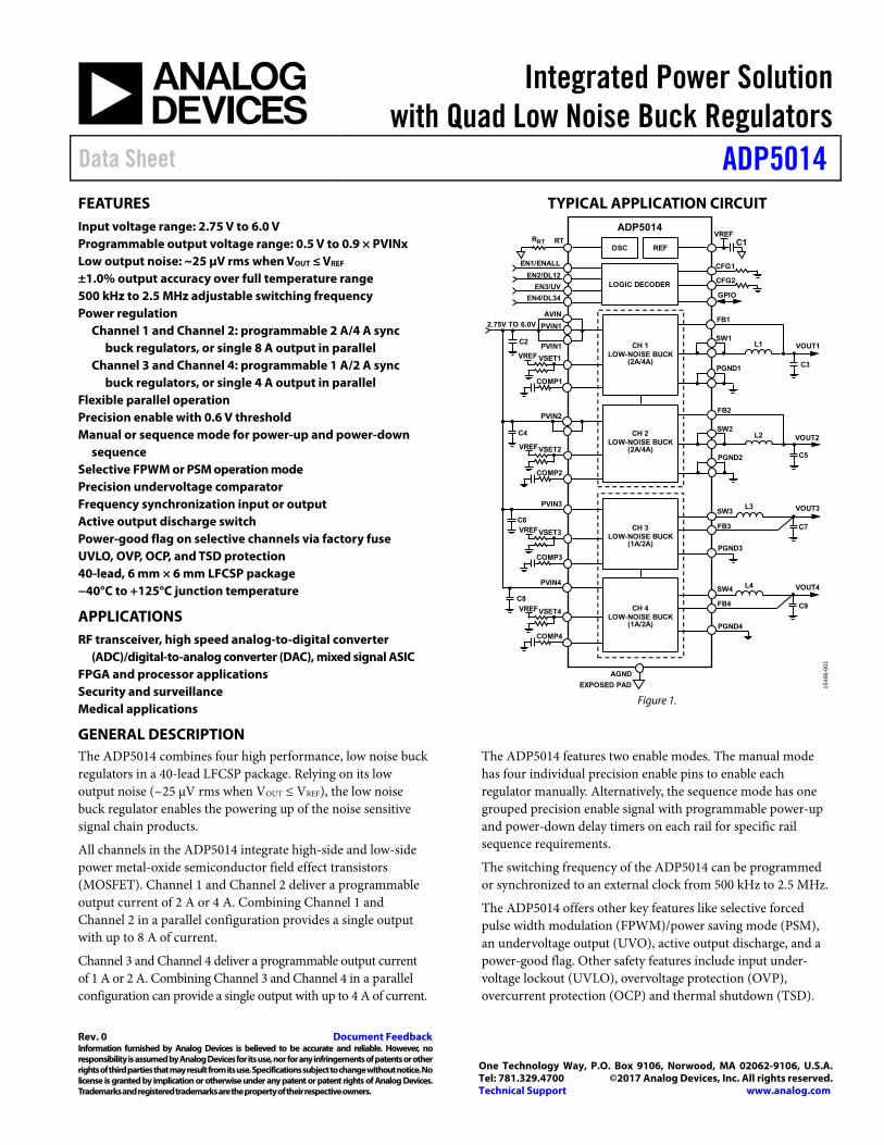
TYPICAL APPLICATION CIRCUIT
L1
GPIO
AVINFB1
SW1
L4SW4
FB4
PGND4
PVIN1
COMP1
PVIN2
PVIN3
PVIN4
C2
C3
C4
C8C9
2.75V TO 6.0V
VOUT1
VOUT4
L3
L2
SW3
SW2
FB3
FB2
PGND3
PGND2
C7
C5
VOUT3
VOUT2
AGND
EXPOSED PAD
ADP5014
PGND1
EN3/UV
EN2/DL12
VSET1
CH 1LOW-NOISE BUCK
(2A/4A)
CH 2LOW-NOISE BUCK
(2A/4A)
CH 3LOW-NOISE BUCK
(1A/2A)
CH 4LOW-NOISE BUCK
(1A/2A)
EN1/ENALL
EN4/DL34
VREF
VREF
CFG1
CFG2
RT C1REFOSC
LOGIC DECODER
RRT
COMP2
VSET2VREF
COMP3
VSET3VREF
COMP4
VSET4VREF
C6
1549
6-00
1
PVIN1
Figure 1.
GENERAL DESCRIPTION The ADP5014 combines four high performance, low noise buck regulators in a 40-lead LFCSP package. Relying on its low output noise (~25 μV rms when VOUT ≤ VREF), the low noise buck regulator enables the powering up of the noise sensitive signal chain products.
All channels in the ADP5014 integrate high-side and low-side power metal-oxide semiconductor field effect transistors (MOSFET). Channel 1 and Channel 2 deliver a programmable output current of 2 A or 4 A. Combining Channel 1 and Channel 2 in a parallel configuration provides a single output with up to 8 A of current.
Channel 3 and Channel 4 deliver a programmable output current of 1 A or 2 A. Combining Channel 3 and Channel 4 in a parallel configuration can provide a single output with up to 4 A of current.
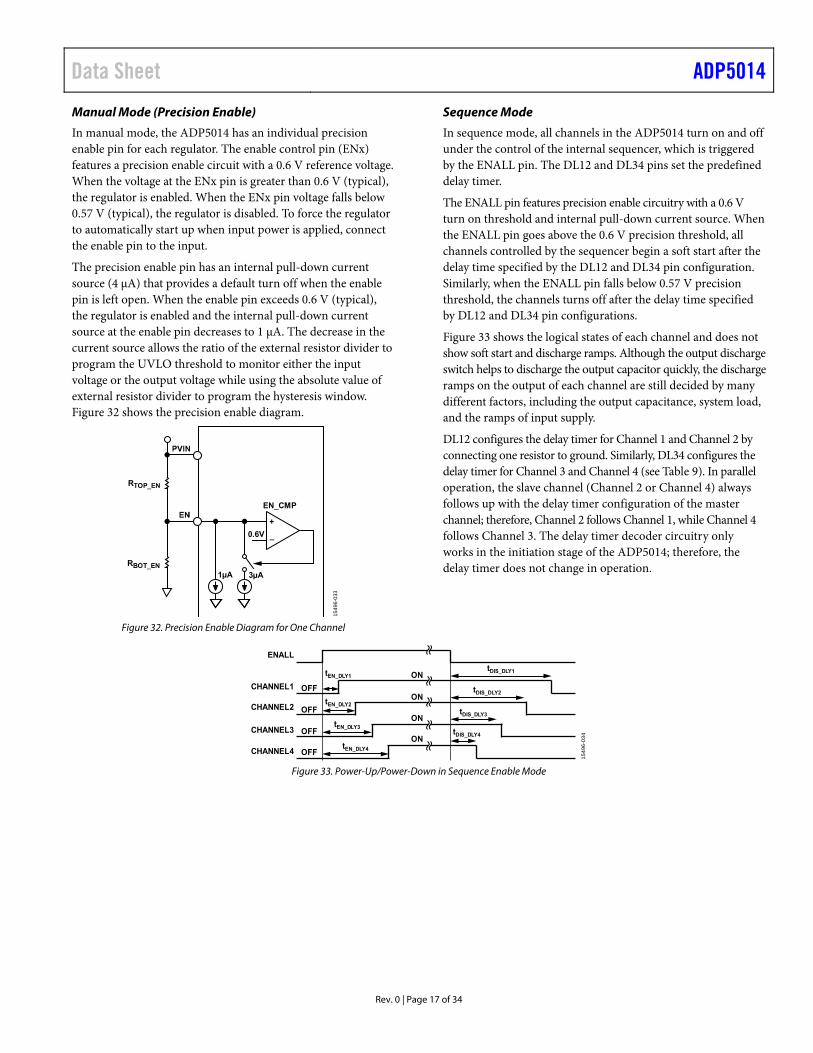
The ADP5014 features two enable modes. The manual mode has four individual precision enable pins to enable each regulator manually. Alternatively, the sequence mode has one grouped precision enable signal with programmable power-up and power-down delay timers on each rail for specific rail sequence requirements.
The switching frequency of the ADP5014 can be programmed or synchronized to an external clock from 500 kHz to 2.5 MHz.
The ADP5014 offers other key features like selective forced pulse width modulation (FPWM)/power saving mode (PSM), an undervoltage output (UVO), active output discharge, and a power-good flag. Other safety features include input under-voltage lockout (UVLO), overvoltage protection (OVP), overcurrent protection (OCP) and thermal shutdown (TSD).
ADP5014 Data Sheet
Rev. 0 | Page 2 of 34
TABLE OF CONTENTS Features .............................................................................................. 1
Applications ....................................................................................... 1
Typical Application Circuit ............................................................. 1
General Description ......................................................................... 1
Revision History ............................................................................... 2
Detailed Functional Block Diagram .............................................. 3
Specifications ..................................................................................... 4
Buck Regulator Specifications .................................................... 5
Absolute Maximum Ratings ............................................................ 7
Thermal Resistance ...................................................................... 7
ESD Caution .................................................................................. 7
Pin Configuration and Function Descriptions ............................. 8
Typical Performance Characteristics ........................................... 10
Theory of Operation ...................................................................... 14
Buck Regulator Operational Modes ......................................... 14
Low Noise Architecture ............................................................. 14
Internal Reference (VREF) ........................................................ 14
Adjustable Output Voltage ........................................................ 14
Function Configurations (CFG1 and CFG2) ......................... 15
Parallel Operation....................................................................... 16
Manual/Sequence Mode ............................................................ 16
General Purpose Input/Output (GPIO) .................................. 18
Oscillator ..................................................................................... 18
Synchronization Input/Output ................................................. 19
Power-Good Function ............................................................... 19
UV Comparator (Sequence Mode Only) ................................ 19
Soft Start ...................................................................................... 20
Startup with Precharged Output .............................................. 20
Current-Limit Protection .......................................................... 20
Frequency Fold Back .................................................................. 20
Short-Circuit Protection (SCP) ................................................ 20
Overvoltage Protection .............................................................. 20
Undervoltage Lockout ............................................................... 20
Active Output Discharge Switch .............................................. 21
Thermal Shutdown .................................................................... 21
Applications Information .............................................................. 22
ADIsimPower Design Tool ....................................................... 22
Programming the Output Voltage ........................................... 22
Voltage Conversion Limitations ............................................... 22
Current-Limit Setting ................................................................ 23
Soft Start Setting ......................................................................... 23
Inductor Selection ...................................................................... 23
Output Capacitor Selection ....................................................... 24
Input Capacitor Selection .......................................................... 24
Programming the UVLO Input ................................................ 24
Compensation Components Design ....................................... 24
Power Dissipation....................................................................... 25
Junction Temperature ................................................................ 26
Design Examples ............................................................................ 27
Setting the Switching Frequency .............................................. 27
Setting the Output Voltage ........................................................ 27
Setting the Configuations (CFG1 and CFG2) ........................ 27
Selecting the Inductor ................................................................ 27
Selecting the Output Capacitor ................................................ 28
Designing the Compensation Network ................................... 28
Low Noise Output Design ......................................................... 28
PCB Layout Recommendations .................................................... 30
Typical Application Circuits ......................................................... 31
Factory Programmable Options ................................................... 33
Factory Default Options ............................................................ 33
Outline Dimensions ....................................................................... 34
Ordering Guide .......................................................................... 34
REVISION HISTORY 6/2017—Revision 0: Initial Version
Data Sheet ADP5014
Rev. 0 | Page 3 of 34
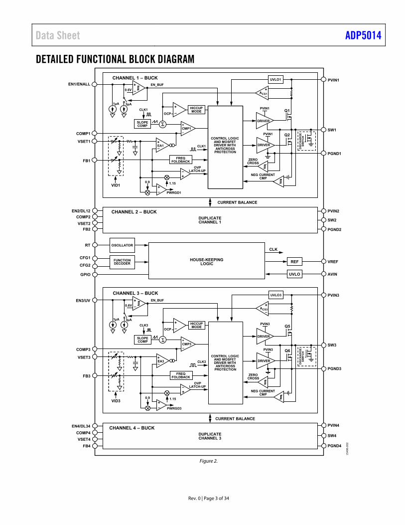
DETAILED FUNCTIONAL BLOCK DIAGRAM
+
–
UVLO1 PVIN1
SW1PVIN1
DRIVER
DRIVER
PGND1
0.6V
HICCUPMODE
+
–OCPCLK1
SLOPECOMP
CLK1
PWRGD1
ZEROCROSS
+
–
+–
FREQFOLDBACK
+
–
CHANNEL 1 – BUCK
DUPLICATECHANNEL 1
CHANNEL 2 – BUCK
CURRENT BALANCE
CURRENT BALANCE
PGND2
PVIN2
SW2
VID1
OVPLATCH-UP
+–
EA1
CMP1
OSCILLATOR
FUNCTIONDECODER
AVIN
VREFHOUSE-KEEPINGLOGIC
ACS1
UVLO
PVIN1Q1
Q2
0.9 1.15
1µA 3µA
EN_BUF
REF
PVIN3
SW3
PGND3
PGND4
PVIN4
SW4
EN1/ENALL
CLK
DUPLICATECHANNEL 3
CHANNEL 4 – BUCK
+
–
+
–
UVLO3
PVIN3
DRIVER
DRIVER
0.6V
HICCUPMODE
+
–OCPCLK3
SLOPECOMP
CLK3
PWRGD3
ZEROCROSS
+
–
+–
FREQFOLDBACK
+
–
CHANNEL 3 – BUCK
VID3
OVPLATCH-UP
+–
EA3
CMP3
ACS3
PVIN3Q5
Q6
0.9 1.15
CONTROL LOGICAND MOSFETDRIVER WITHANTICROSS
PROTECTION
CONTROL LOGICAND MOSFETDRIVER WITHANTICROSS
PROTECTION
NEG CURRENTCMP
NEG CURRENTCMP
DIS
CH
AR
GE
SW
ITC
HD
ISC
HA
RG
ES
WIT
CH
1µA 3µA
EN_BUF+
–
COMP1
VSET1
FB1
EN2/DL12
COMP2
VSET2
FB2
RT
CFG1
CFG2
GPIO
EN3/UV
COMP3
VSET3
FB3
EN4/DL34
COMP4
VSET4
FB4
1549
6-00
2
Figure 2.
ADP5014 Data Sheet
Rev. 0 | Page 4 of 34
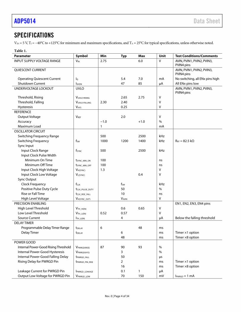
SPECIFICATIONS VIN = 5 V, TJ = −40°C to +125°C for minimum and maximum specifications, and TA = 25°C for typical specifications, unless otherwise noted.
Table 1. Parameter Symbol Min Typ Max Unit Test Conditions/Comments INPUT SUPPLY VOLTAGE RANGE VIN 2.75 6.0 V AVIN, PVIN1, PVIN2, PVIN3,
PVIN4 pins QUIESCENT CURRENT AVIN, PVIN1, PVIN2, PVIN3,
PVIN4 pins Operating Quiescent Current IQ 5.4 7.0 mA No switching, all ENx pins high Shutdown Current ISHDN 47 85 μA All ENx pins low
UNDERVOLTAGE LOCKOUT UVLO AVIN, PVIN1, PVIN2, PVIN3, PVIN4 pins
Threshold, Rising VUVLO-RISING 2.65 2.75 V Threshold, Falling VUVLO-FALLING 2.30 2.40 V Hysteresis VHYS 0.25 V
REFERENCE Output Voltage VREF 2.0 V Accuracy −1.0 +1.0 % Maximum Load 1 mA
OSCILLATOR CIRCUIT Switching Frequency Range 500 2500 kHz Switching Frequency fSW 1000 1200 1400 kHz RRT = 82.5 kΩ Sync Input
Input Clock Range fSYNC 500 2500 kHz Input Clock Pulse Width
Minimum On Time tSYNC_MIN_ON 100 ns Minimum Off Time tSYNC_MIN_OFF 100 ns
Input Clock High Voltage VH(SYNC) 1.3 V Input Clock Low Voltage VL(SYNC) 0.4 V
Sync Output Clock Frequency fCLK fSW kHz Positive Pulse Duty Cycle tCLK_PULSE_DUTY 50 % Rise or Fall Time tCLK_RISE_FALL 10 ns High Level Voltage VH(SYNC_OUT) VAVIN V
PRECISION ENABLING EN1, EN2, EN3, EN4 pins High Level Threshold VTH_H(EN) 0.6 0.65 V Low Level Threshold VTH_L(EN) 0.52 0.57 V Source Current ITH_L(EN) 4 μA Below the falling threshold
DELAY TIMER Programmable Delay Timer Range tDELAY 6 48 ms Delay Timer tDELAY 6 ms Timer ×1 option 48 ms Timer ×8 option
POWER GOOD Internal Power-Good Rising Threshold VPWRGD(RISE) 87 90 93 % Internal Power-Good Hysteresis VPWRGD(HYS) 3 % Internal Power-Good Falling Delay tPWRGD_FALL 50 μs Rising Delay for PWRGD Pin tPWRGD_PIN_RISE 2 ms Timer ×1 option 16 ms Timer ×8 option Leakage Current for PWRGD Pin IPWRGD_LEAKAGE 0.1 1 μA Output Low Voltage for PWRGD Pin VPWRGD_LOW 70 150 mV IPWRGD = 1 mA
Data Sheet ADP5014
Rev. 0 | Page 5 of 34
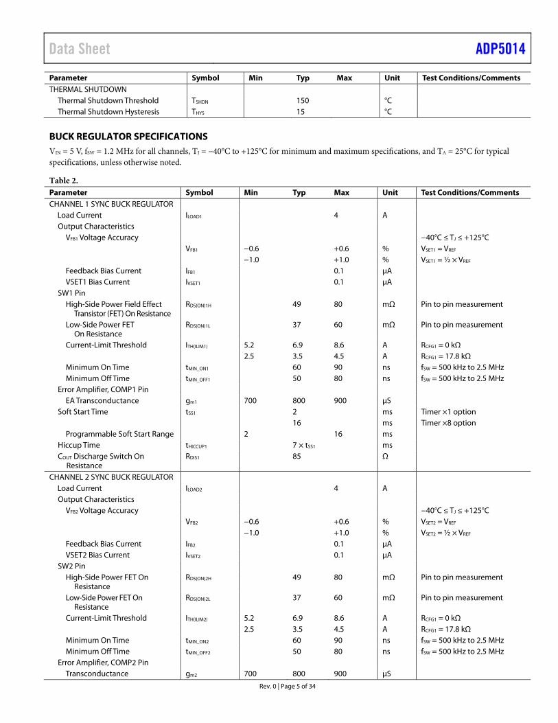
Parameter Symbol Min Typ Max Unit Test Conditions/Comments THERMAL SHUTDOWN
Thermal Shutdown Threshold TSHDN 150 °C Thermal Shutdown Hysteresis THYS 15 °C
BUCK REGULATOR SPECIFICATIONS VIN = 5 V, fSW = 1.2 MHz for all channels, TJ = −40°C to +125°C for minimum and maximum specifications, and TA = 25°C for typical specifications, unless otherwise noted.
Table 2. Parameter Symbol Min Typ Max Unit Test Conditions/Comments CHANNEL 1 SYNC BUCK REGULATOR
Load Current ILOAD1 4 A Output Characteristics
VFB1 Voltage Accuracy −40°C ≤ TJ ≤ +125°C VFB1 −0.6 +0.6 % VSET1 = VREF −1.0 +1.0 % VSET1 = ½ × VREF Feedback Bias Current IFB1 0.1 μA VSET1 Bias Current IVSET1 0.1 μA
SW1 Pin High-Side Power Field Effect
Transistor (FET) On Resistance RDS(ON)1H 49 80 mΩ Pin to pin measurement
Low-Side Power FET On Resistance
RDS(ON)1L 37 60 mΩ Pin to pin measurement
Current-Limit Threshold ITH(ILIM1) 5.2 6.9 8.6 A RCFG1 = 0 kΩ 2.5 3.5 4.5 A RCFG1 = 17.8 kΩ Minimum On Time tMIN_ON1 60 90 ns fSW = 500 kHz to 2.5 MHz Minimum Off Time tMIN_OFF1 50 80 ns fSW = 500 kHz to 2.5 MHz
Error Amplifier, COMP1 Pin EA Transconductance gm1 700 800 900 μS
Soft Start Time tSS1 2 ms Timer ×1 option 16 ms Timer ×8 option
Programmable Soft Start Range 2 16 ms Hiccup Time tHICCUP1 7 × tSS1 ms COUT Discharge Switch On
Resistance RDIS1 85 Ω
CHANNEL 2 SYNC BUCK REGULATOR Load Current ILOAD2 4 A Output Characteristics
VFB2 Voltage Accuracy −40°C ≤ TJ ≤ +125°C VFB2 −0.6 +0.6 % VSET2 = VREF −1.0 +1.0 % VSET2 = ½ × VREF Feedback Bias Current IFB2 0.1 μA VSET2 Bias Current IVSET2 0.1 μA
SW2 Pin High-Side Power FET On
Resistance RDS(ON)2H 49 80 mΩ Pin to pin measurement
Low-Side Power FET On Resistance
RDS(ON)2L 37 60 mΩ Pin to pin measurement
Current-Limit Threshold ITH(ILIM2) 5.2 6.9 8.6 A RCFG1 = 0 kΩ 2.5 3.5 4.5 A RCFG1 = 17.8 kΩ Minimum On Time tMIN_ON2 60 90 ns fSW = 500 kHz to 2.5 MHz Minimum Off Time tMIN_OFF2 50 80 ns fSW = 500 kHz to 2.5 MHz
Error Amplifier, COMP2 Pin Transconductance gm2 700 800 900 μS
ADP5014 Data Sheet
Rev. 0 | Page 6 of 34
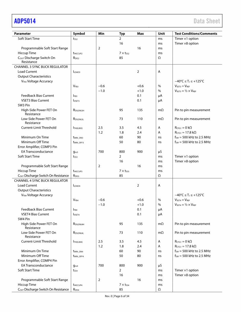
Parameter Symbol Min Typ Max Unit Test Conditions/Comments Soft Start Time tSS2 2 ms Timer ×1 option 16 ms Timer ×8 option
Programmable Soft Start Range 2 16 ms Hiccup Time tHICCUP2 7 × tSS2 ms COUT Discharge Switch On
Resistance RDIS2 85 Ω
CHANNEL 3 SYNC BUCK REGULATOR Load Current ILOAD3 2 A Output Characteristics
VFB3 Voltage Accuracy −40°C ≤ TJ ≤ +125°C VFB3 −0.6 +0.6 % VSET3 = VREF −1.0 +1.0 % VSET3 = ½ × VREF
Feedback Bias Current IFB3 0.1 μA VSET3 Bias Current IVSET3 0.1 μA
SW3 Pin High-Side Power FET On
Resistance RDS(ON)3H 95 135 mΩ Pin to pin measurement
Low-Side Power FET On Resistance
RDS(ON)3L 73 110 mΩ Pin to pin measurement
Current-Limit Threshold ITH(ILIM3) 2.5 3.5 4.5 A RCFG1 = 0 kΩ 1.2 1.8 2.4 A RCFG1 = 17.8 kΩ Minimum On Time tMIN_ON3 60 90 ns fSW = 500 kHz to 2.5 MHz Minimum Off Time tMIN_OFF3 50 80 ns fSW = 500 kHz to 2.5 MHz
Error Amplifier, COMP3 Pin EA Transconductance gm3 700 800 900 μS
Soft Start Time tSS3 2 ms Timer ×1 option 16 ms Timer ×8 option
Programmable Soft Start Range 2 16 ms Hiccup Time tHICCUP3 7 × tSS3 ms COUT Discharge Switch On Resistance RDIS3 85 Ω
CHANNEL 4 SYNC BUCK REGULATOR Load Current ILOAD4 2 A Output Characteristics
VFB4 Voltage Accuracy −40°C ≤ TJ ≤ +125°C VFB4 −0.6 +0.6 % VSET4 = VREF −1.0 +1.0 % VSET4 = ½ × VREF Feedback Bias Current IFB4 0.1 μA VSET4 Bias Current IVSET4 0.1 μA
SW4 Pin High-Side Power FET On
Resistance RDS(ON)4H 95 135 mΩ Pin to pin measurement
Low-Side Power FET On Resistance
RDS(ON)4L 73 110 mΩ Pin to pin measurement
Current-Limit Threshold ITH(ILIM4) 2.5 3.5 4.5 A RCFG1 = 0 kΩ 1.2 1.8 2.4 A RCFG1 = 17.8 kΩ Minimum On Time tMIN_ON4 60 90 ns fSW = 500 kHz to 2.5 MHz Minimum Off Time tMIN_OFF4 50 80 ns fSW = 500 kHz to 2.5 MHz
Error Amplifier, COMP4 Pin EA Transconductance gm4 700 800 900 μS
Soft Start Time tSS4 2 ms Timer ×1 option 16 ms Timer ×8 option
Programmable Soft Start Range 2 16 ms Hiccup Time tHICCUP4 7 × tSS4 ms COUT Discharge Switch On Resistance RDIS4 85 Ω
Data Sheet ADP5014
Rev. 0 | Page 7 of 34
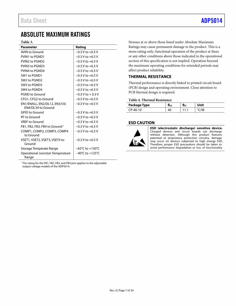
ABSOLUTE MAXIMUM RATINGS Table 3. Parameter Rating AVIN to Ground −0.3 V to +6.5 V PVIN1 to PGND1 −0.3 V to +6.5 V PVIN2 to PGND2 −0.3 V to +6.5 V PVIN3 to PGND3 −0.3 V to +6.5 V PVIN4 to PGND4 −0.3 V to +6.5 V SW1 to PGND1 −0.3 V to +6.5 V SW2 to PGND2 −0.3 V to +6.5 V SW3 to PGND3 −0.3 V to +6.5 V SW4 to PGND4 −0.3 V to +6.5 V PGND to Ground −0.3 V to + 0.3 V CFG1, CFG2 to Ground −0.3 V to +6.5 V EN1/ENALL, EN2/DL12, EN3/UV,
EN4/DL34 to Ground −0.3 V to +6.5 V
GPIO to Ground −0.3 V to +6.5 V RT to Ground −0.3 V to +6.5 V VREF to Ground −0.3 V to +6.5 V FB1, FB2, FB3, FB4 to Ground 1 −0.3 V to +6.5 V COMP1, COMP2, COMP3, COMP4
to Ground −0.3 V to +6.5 V
VSET1, VSET2, VSET3, VSET4 to Ground
−0.3 V to +6.5 V
Storage Temperate Range −65°C to +150°C Operational Junction Temperature
Range −40°C to +125°C
1 The rating for the FB1, FB2, FB3, and FB4 pins applies to the adjustable
output voltage models of the ADP5014.
Stresses at or above those listed under Absolute Maximum Ratings may cause permanent damage to the product. This is a stress rating only; functional operation of the product at these or any other conditions above those indicated in the operational section of this specification is not implied. Operation beyond the maximum operating conditions for extended periods may affect product reliability.
THERMAL RESISTANCE Thermal performance is directly linked to printed circuit board (PCB) design and operating environment. Close attention to PCB thermal design is required.
Table 4. Thermal Resistance Package Type θJA θJC Unit CP-40-10 40 11.1 °C/W
ESD CAUTION
ADP5014 Data Sheet
Rev. 0 | Page 8 of 34
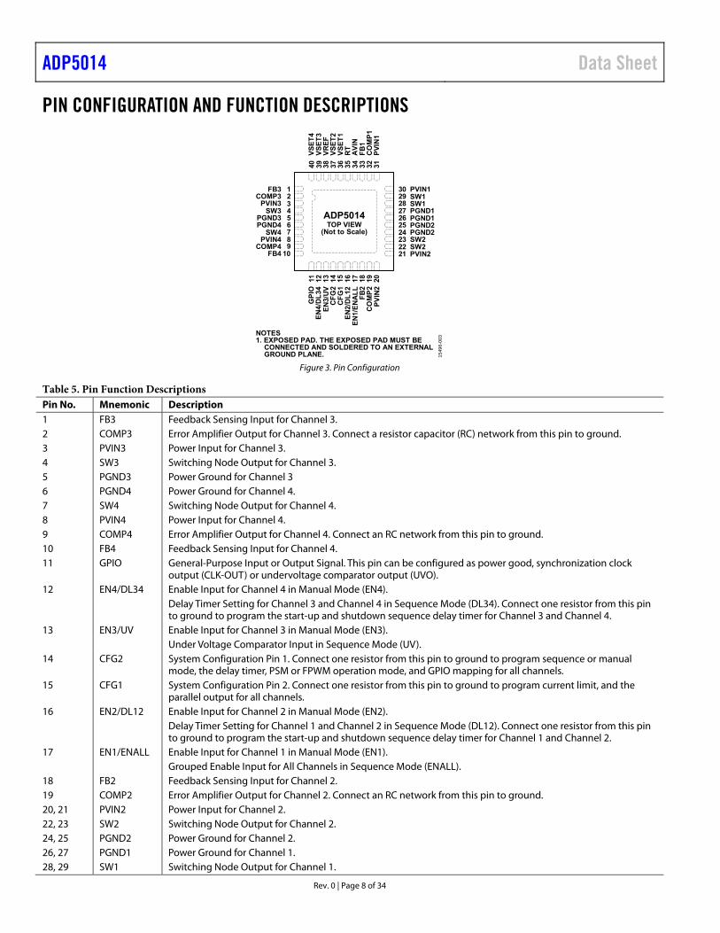
PIN CONFIGURATION AND FUNCTION DESCRIPTIONS
123456789
10
2324252627282930
2221
11 21 31 51 7161 81 91 024 1
3343536373839304 23 13
ADP5014TOP VIEW
(Not to Scale)
FB3 PVIN1
NOTES1. EXPOSED PAD. THE EXPOSED PAD MUST BE CONNECTED AND SOLDERED TO AN EXTERNAL GROUND PLANE.
GP
IOV
SE
T4
COMP3PVIN3
SW3PGND3PGND4
SW4PVIN4
COMP4FB4
VS
ET
3V
RE
FV
SE
T2
VS
ET
1R
TA
VIN
FB
1C
OM
P1
PV
IN1
SW1SW1PGND1PGND1PGND2PGND2SW2SW2PVIN2
EN
4/D
L34
EN
3/U
VC
FG
2C
FG
1E
N2/
DL
12E
N1/
EN
AL
LF
B2
CO
MP
2P
VIN
2
1549
6-00
3
Figure 3. Pin Configuration
Table 5. Pin Function Descriptions Pin No. Mnemonic Description 1 FB3 Feedback Sensing Input for Channel 3. 2 COMP3 Error Amplifier Output for Channel 3. Connect a resistor capacitor (RC) network from this pin to ground. 3 PVIN3 Power Input for Channel 3. 4 SW3 Switching Node Output for Channel 3. 5 PGND3 Power Ground for Channel 3 6 PGND4 Power Ground for Channel 4. 7 SW4 Switching Node Output for Channel 4. 8 PVIN4 Power Input for Channel 4. 9 COMP4 Error Amplifier Output for Channel 4. Connect an RC network from this pin to ground. 10 FB4 Feedback Sensing Input for Channel 4. 11 GPIO General-Purpose Input or Output Signal. This pin can be configured as power good, synchronization clock
output (CLK-OUT) or undervoltage comparator output (UVO). 12 EN4/DL34 Enable Input for Channel 4 in Manual Mode (EN4). Delay Timer Setting for Channel 3 and Channel 4 in Sequence Mode (DL34). Connect one resistor from this pin
to ground to program the start-up and shutdown sequence delay timer for Channel 3 and Channel 4. 13 EN3/UV Enable Input for Channel 3 in Manual Mode (EN3). Under Voltage Comparator Input in Sequence Mode (UV). 14 CFG2 System Configuration Pin 1. Connect one resistor from this pin to ground to program sequence or manual
mode, the delay timer, PSM or FPWM operation mode, and GPIO mapping for all channels. 15 CFG1 System Configuration Pin 2. Connect one resistor from this pin to ground to program current limit, and the
parallel output for all channels. 16 EN2/DL12 Enable Input for Channel 2 in Manual Mode (EN2). Delay Timer Setting for Channel 1 and Channel 2 in Sequence Mode (DL12). Connect one resistor from this pin
to ground to program the start-up and shutdown sequence delay timer for Channel 1 and Channel 2. 17 EN1/ENALL Enable Input for Channel 1 in Manual Mode (EN1). Grouped Enable Input for All Channels in Sequence Mode (ENALL). 18 FB2 Feedback Sensing Input for Channel 2. 19 COMP2 Error Amplifier Output for Channel 2. Connect an RC network from this pin to ground. 20, 21 PVIN2 Power Input for Channel 2. 22, 23 SW2 Switching Node Output for Channel 2. 24, 25 PGND2 Power Ground for Channel 2. 26, 27 PGND1 Power Ground for Channel 1. 28, 29 SW1 Switching Node Output for Channel 1.
Data Sheet ADP5014
Rev. 0 | Page 9 of 34
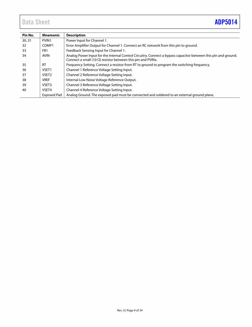
Pin No. Mnemonic Description 30, 31 PVIN1 Power Input for Channel 1. 32 COMP1 Error Amplifier Output for Channel 1. Connect an RC network from this pin to ground. 33 FB1 Feedback Sensing Input for Channel 1. 34 AVIN Analog Power Input for the Internal Control Circuitry. Connect a bypass capacitor between this pin and ground.
Connect a small (10 Ω) resistor between this pin and PVINx. 35 RT Frequency Setting. Connect a resistor from RT to ground to program the switching frequency. 36 VSET1 Channel 1 Reference Voltage Setting Input. 37 VSET2 Channel 2 Reference Voltage Setting Input. 38 VREF Internal Low Noise Voltage Reference Output. 39 VSET3 Channel 3 Reference Voltage Setting Input. 40 VSET4 Channel 4 Reference Voltage Setting Input. Exposed Pad Analog Ground. The exposed pad must be connected and soldered to an external ground plane.
ADP5014 Data Sheet
Rev. 0 | Page 10 of 34
TYPICAL PERFORMANCE CHARACTERISTICS
0
10
20
30
40
50
60
70
80
90
100
0 1.0 2.0 3.0 4.0
EF
FIC
IEN
CY
(%
)
IOUT (A)
VOUT = 1.2VVOUT = 1.5VVOUT = 1.8VVOUT = 2.5VVOUT = 3.3V
1549
6-00
4
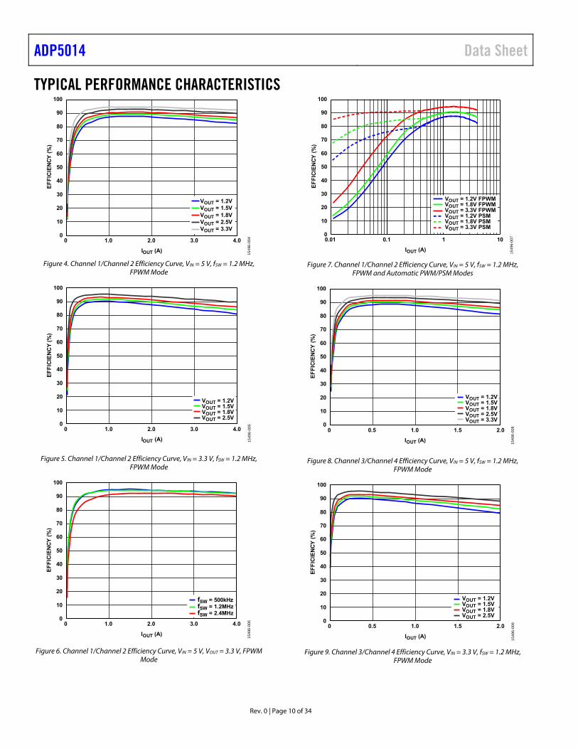
Figure 4. Channel 1/Channel 2 Efficiency Curve, VIN = 5 V, fSW = 1.2 MHz, FPWM Mode
0
10
20
30
40
50
60
70
80
90
100
0 1.0 2.0 3.0 4.0
EF
FIC
IEN
CY
(%
)
IOUT (A)
VOUT = 1.2VVOUT = 1.5VVOUT = 1.8VVOUT = 2.5V
1549
6-00
5
Figure 5. Channel 1/Channel 2 Efficiency Curve, VIN = 3.3 V, fSW = 1.2 MHz, FPWM Mode
0
10
20
30
40
50
60
70
80
90
100
0 1.0 2.0 3.0 4.0
EF
FIC
IEN
CY
(%
)
fSW = 500kHzfSW = 1.2MHzfSW = 2.4MHz
IOUT (A)
1549
6-00
6
Figure 6. Channel 1/Channel 2 Efficiency Curve, VIN = 5 V, VOUT = 3.3 V, FPWM Mode
0
10
20
30
40
50
60
70
80
90
100
0.01 0.1 1 10
EF
FIC
IEN
CY
(%
)
IOUT (A)
VOUT = 1.2V FPWMVOUT = 1.8V FPWMVOUT = 3.3V FPWMVOUT = 1.2V PSMVOUT = 1.8V PSMVOUT = 3.3V PSM
1549
6-00
7
Figure 7. Channel 1/Channel 2 Efficiency Curve, VIN = 5 V, fSW = 1.2 MHz, FPWM and Automatic PWM/PSM Modes
0
10
20
30
40
50
60
70
80
90
100
0 0.5 1.0 1.5 2.0
EF
FIC
IEN
CY
(%
)
VOUT = 1.2VVOUT = 1.5VVOUT = 1.8VVOUT = 2.5VVOUT = 3.3V
IOUT (A) 1549
6-00
8
Figure 8. Channel 3/Channel 4 Efficiency Curve, VIN = 5 V, fSW = 1.2 MHz, FPWM Mode
0
10
20
30
40
50
60
70
80
90
100
0 0.5 1.0 1.5
EF
FIC
IEN
CY
(%
)
VOUT = 1.2VVOUT = 1.5VVOUT = 1.8VVOUT = 2.5V
2.0
IOUT (A)
1549
6-00
9
Figure 9. Channel 3/Channel 4 Efficiency Curve, VIN = 3.3 V, fSW = 1.2 MHz, FPWM Mode
Data Sheet ADP5014
Rev. 0 | Page 11 of 34
0
10
20
30
40
50
60
70
80
90
100
0 0.5 1.0 1.5 2.0
EF
FIC
IEN
CY
(%
)
fSW = 500kHzfSW = 1.2MHzfSW = 2.5MHz
IOUT (A)
1549
6-01
0
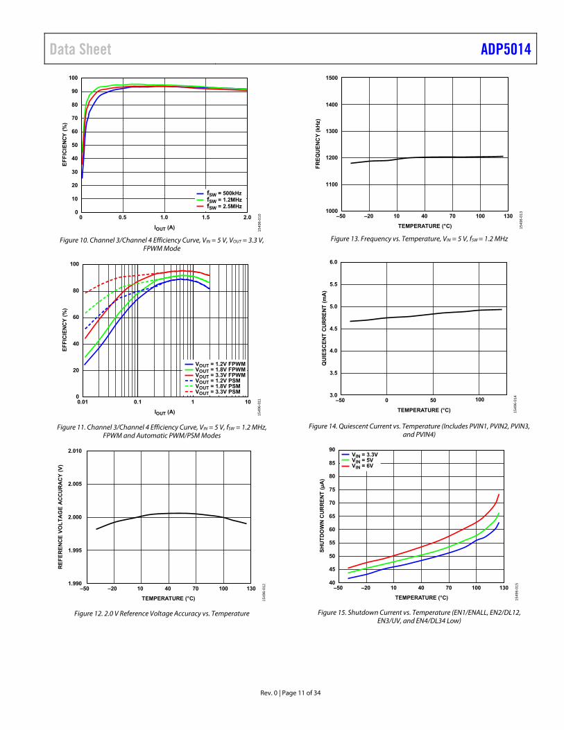
Figure 10. Channel 3/Channel 4 Efficiency Curve, VIN = 5 V, VOUT = 3.3 V, FPWM Mode
0
20
40
60
80
100
0.01 0.1 1 10
EF
FIC
IEN
CY
(%
)
IOUT (A)
VOUT = 1.2V FPWMVOUT = 1.8V FPWMVOUT = 3.3V FPWMVOUT = 1.2V PSMVOUT = 1.8V PSMVOUT = 3.3V PSM
1549
6-01
1
Figure 11. Channel 3/Channel 4 Efficiency Curve, VIN = 5 V, fSW = 1.2 MHz, FPWM and Automatic PWM/PSM Modes
1.990
1.995
2.000
2.005
2.010
–50 –20 10 40 70 100 130
RE
FE
RE
NC
E V
OL
TA
GE
AC
CU
RA
CY
(V
)
TEMPERATURE (°C) 1549
6-01
2
Figure 12. 2.0 V Reference Voltage Accuracy vs. Temperature
TEMPERATURE (°C)
1000
1100
1200
1300
1400
1500
–50 –20 10 40 70 100 130
FR
EQ
UE
NC
Y (
kHz)
1549
6-01
3
Figure 13. Frequency vs. Temperature, VIN = 5 V, fSW = 1.2 MHz
TEMPERATURE (°C)
3.0
3.5
4.0
4.5
5.0
5.5
6.0
–50 0 50 100
QU
IES
CE
NT
CU
RR
EN
T (
mA
)
1549
6-01
4
Figure 14. Quiescent Current vs. Temperature (Includes PVIN1, PVIN2, PVIN3, and PVIN4)
TEMPERATURE (°C)
40
45
50
55
60
65
70
75
80
85
90
–50 –20 10 40 70 100 130
SH
UT
DO
WN
CU
RR
EN
T (
µA
)
VIN = 3.3VVIN = 5VVIN = 6V
1549
6-01
5
Figure 15. Shutdown Current vs. Temperature (EN1/ENALL, EN2/DL12, EN3/UV, and EN4/DL34 Low)
ADP5014 Data Sheet
Rev. 0 | Page 12 of 34
TEMPERATURE (°C)
2.0
2.1
2.2
2.3
2.4
2.5
2.6
2.7
2.8
2.9
3.0
–50 –20 10 40 70 100 130
UV
LO
TH
RE
SH
OL
D (
V)
RISINGFALLING
1549
6-01
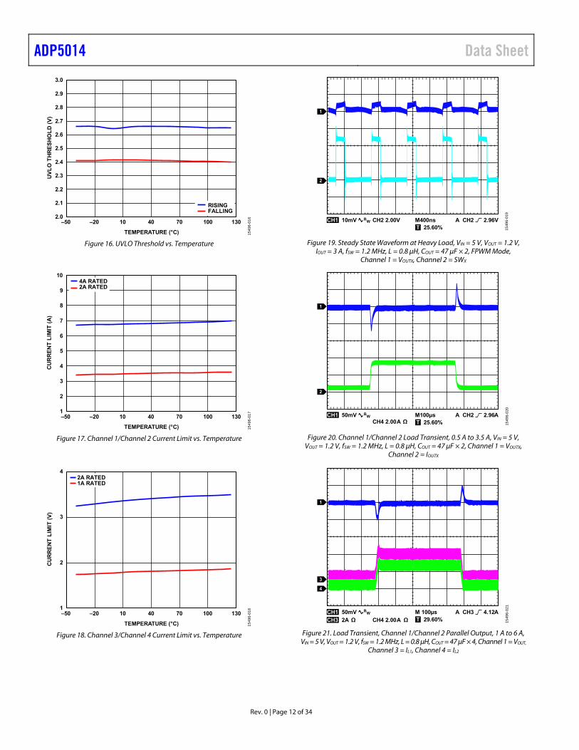
6Figure 16. UVLO Threshold vs. Temperature
TEMPERATURE (°C)
1
2
3
4
5
6
7
8
9
10
–50 –20 10 40 70 100 130
CU
RR
EN
T L
IMIT
(A
)
4A RATED2A RATED
1549
6-01
7
Figure 17. Channel 1/Channel 2 Current Limit vs. Temperature
TEMPERATURE (°C)
1
2
3
4
–50 –20 10 40 70 100 130
CU
RR
EN
T L
IMIT
(V
)
2A RATED1A RATED
1549
6-01
8
Figure 18. Channel 3/Channel 4 Current Limit vs. Temperature
CH1 10mV CH2 2.00V M400ns A CH2 2.96V
1
2
T 25.60%
BW
1549
6-01
9
Figure 19. Steady State Waveform at Heavy Load, VIN = 5 V, VOUT = 1.2 V, IOUT = 3 A, fSW = 1.2 MHz, L = 0.8 μH, COUT = 47 μF × 2, FPWM Mode,
Channel 1 = VOUTX, Channel 2 = SWX
CH1 50mVCH4 2.00A
M100µs A CH2 2.96A
1
2
T 25.60%
BW
Ω 1549
6-02
0
Figure 20. Channel 1/Channel 2 Load Transient, 0.5 A to 3.5 A, VIN = 5 V, VOUT = 1.2 V, fSW = 1.2 MHz, L = 0.8 μH, COUT = 47 μF × 2, Channel 1 = VOUTX,
Channel 2 = IOUTX
CH1 50mV M 100µs A CH3 4.12A
1
3
4
T 29.60%
BW
CH3 2A CH4 2.00A ΩΩ 1549
6-02
1
Figure 21. Load Transient, Channel 1/Channel 2 Parallel Output, 1 A to 6 A, VIN = 5 V, VOUT = 1.2 V, fSW = 1.2 MHz, L = 0.8 μH, COUT = 47 μF × 4, Channel 1 = VOUT,
Channel 3 = IL1, Channel 4 = IL2
Data Sheet ADP5014
Rev. 0 | Page 13 of 34
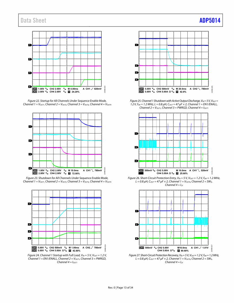
CH1 1.00V CH2 2.00V M 4.00ms A CH1 820mV
1
2
3
4
T 24.20%
BW
CH3 2.00V CH4 2.00VBW
BW
BW 15
496-
022
Figure 22. Startup for All Channels Under Sequence Enable Mode, Channel 1 = VOUT1, Channel 2 = VOUT2, Channel 3 = VOUT3, Channel 4 = VOUT4
CH1 1.00V CH2 2.00V M 10.0ms A CH1 780mV
1
2
3
4
T 72.00%
BW
CH3 2.00V CH4 2.00VBW
BW
BW 15
496-
023
Figure 23. Shutdown for All Channels Under Sequence Enable Mode, Channel 1 = VOUT1, Channel 2 = VOUT2, Channel 3 = VOUT3, Channel 4 = VOUT4
CH1 5.00V CH2 500mV M 1.00ms A CH2 780mV
1
2
3
4
T 42.80%
BW
CH3 5.00V CH4 5.00ABW
BW
BWΩ 15
496-
024
Figure 24. Channel 1 Startup with Full Load, VIN = 5 V, VOUT = 1.2 V, Channel 1 = EN1/ENALL, Channel 2 = VOUT1, Channel 3 = PWRGD,
Channel 4 = IOUT1
CH1 5.00V CH2 500mV M 20.0ms A CH2 780mV
1
2
3
4
T 42.8%
BW
CH3 5.00V CH4 5.00ABW
BW
BWΩ 15
496-
025
Figure 25. Channel 1 Shutdown with Active Output Discharge, VIN = 5 V, VOUT = 1.2 V, fSW = 1.2 MHz, L = 0.8 μH, COUT = 47 μF × 2, Channel 1 = EN1/ENALL,
Channel 2 = VOUT1, Channel 3 = PWRGD, Channel 4 = IOUT1
CH1 500mV CH2 5.00V M 10.0ms A CH1 520mV
1
2
4
T 25.60%
BW
CH4 5.00A BWΩ 15
496-
026
Figure 26. Short-Circuit Protection Entry, VIN = 5 V, VOUT = 1.2 V, fSW = 1.2 MHz, L = 0.8 μH, COUT = 47 μF × 2, Channel 1 = VOUTX, Channel 2 = SWX,
Channel 4 = ILX
CH1 500mV CH2 5.00V M10.0ms A CH1 1.01V
1
2
4
T 80.60%
BW
CH4 5.00A BWΩ 15
496-
027
Figure 27. Short-Circuit Protection Recovery, VIN = 5 V, VOUT = 1.2 V, fSW = 1.2 MHz, L = 0.8 μH, COUT = 47 μF × 2, Channel 1 = VOUTX, Channel 2 = SWX,
Channel 4 = ILX
ADP5014 Data Sheet
Rev. 0 | Page 14 of 34
THEORY OF OPERATION The ADP5014 is a power management unit that combines four high performance, low noise buck regulators in a 40-lead LFCSP package.
BUCK REGULATOR OPERATIONAL MODES PWM Mode
In PWM mode, the buck regulators in the ADP5014 operate at a fixed frequency; this frequency is set by an internal oscillator that is programmed by the RT pin. At the start of each oscillator cycle, the high-side MOSFET switch turns on and sends a positive voltage across the inductor. The inductor current increases until the current sense signal exceeds the peak inductor current threshold that turns off the high-side MOSFET switch. This threshold is set by the error amplifier output. During the high-side MOSFET off time, the inductor current decreases through the low-side MOSFET switch until the next oscillator clock pulse starts a new cycle. The buck regulators in the ADP5014 regulate the output voltage by adjusting the peak inductor current threshold.
PSM Mode
To achieve higher efficiency, the buck regulators in the ADP5014 smoothly transition to variable frequency PSM mode operation when the output load falls below the PSM current threshold. When the output voltage falls below regulation, the buck regulator enters PWM mode for a few oscillator cycles until the voltage increases to within regulation. During the idle time between bursts, the MOSFET switch turns off, and the output capacitor supplies all the output current.
The PSM mode comparator monitors the internal compensation node, which represents the peak inductor current information. The average PSM mode current threshold depends on the input voltage (VIN), the output voltage (VOUT), the inductor, and the output capacitor. Because the output voltage occasionally falls below regulation and then recovers, the output voltage ripple in PSM mode is larger than the ripple in the forced PWM mode of operation under light load conditions.
FPWM and Automatic PWM/PSM Modes
The buck regulators can be configured to always operate in FPWM mode using the CFG2 configuration pin. In forced PWM mode, the regulator continues to operate at a fixed frequency even when the output current is below the PWM/ PSM threshold. In PWM mode, the efficiency is lower compared to PSM mode under light load conditions. The low-side MOSFET remains on when the inductor current falls to less than 0 A, causing the ADP5014 to enter continuous conduction mode (CCM).
The buck regulators can be configured to operate in automatic PWM or PSM mode using the CFG2 configuration pin. In automatic PWM/PSM mode, the buck regulators operate in either PWM mode or PSM mode, depending on the output current. When the average output current falls below the PWM/PSM threshold, the buck regulator enters PSM mode
operation; in PSM mode, the regulator operates with a reduced switching frequency to maintain high efficiency. The low-side MOSFET turns off when the output current reaches 0 A, causing the regulator to operate in discontinuous mode (DCM).
Use the CFG2 pin to configure the operational mode of all four buck regulators to operate in PWM mode or automatic PWM/PSM mode.
LOW NOISE ARCHITECTURE Traditional dc-to-dc or linear regulator output noise is typically proportional to the output voltage setting. The ADP5014 optimizes many analog blocks to achieve lower output noise at low frequency range. The unity-gain voltage reference structure also makes its output noise independent from the output voltage setting when VOUT setting is less than VREF voltage.
The low noise buck regulator enables the device to power up noise sensitive signal chain products directly with excellent output noise performance, ~25 μV rms from 10 Hz to 100 kHz, which is similar or even better than traditional low dropout regulators (LDOs).
The additional LC filter is still required because the fundamental switching output ripple and its harmonic affects signal chain performance and likely generates unexpected spurs. This additional LC filter is typically relatively small due to the high switching frequency operation of the buck regulator in the ADP5014.
INTERNAL REFERENCE (VREF) The ADP5014 provides an accurate, low noise, 2.0 V reference voltage. One 0.47 μF ceramic capacitor must be connected between VREF and ground. A larger value of capacitance provides better noise suppression.
The VREF reference circuitry is mainly designed for internal use and has very limited output load capacity (<1 mA); therefore, check the load capability requirements if VREF is used for other purposes.
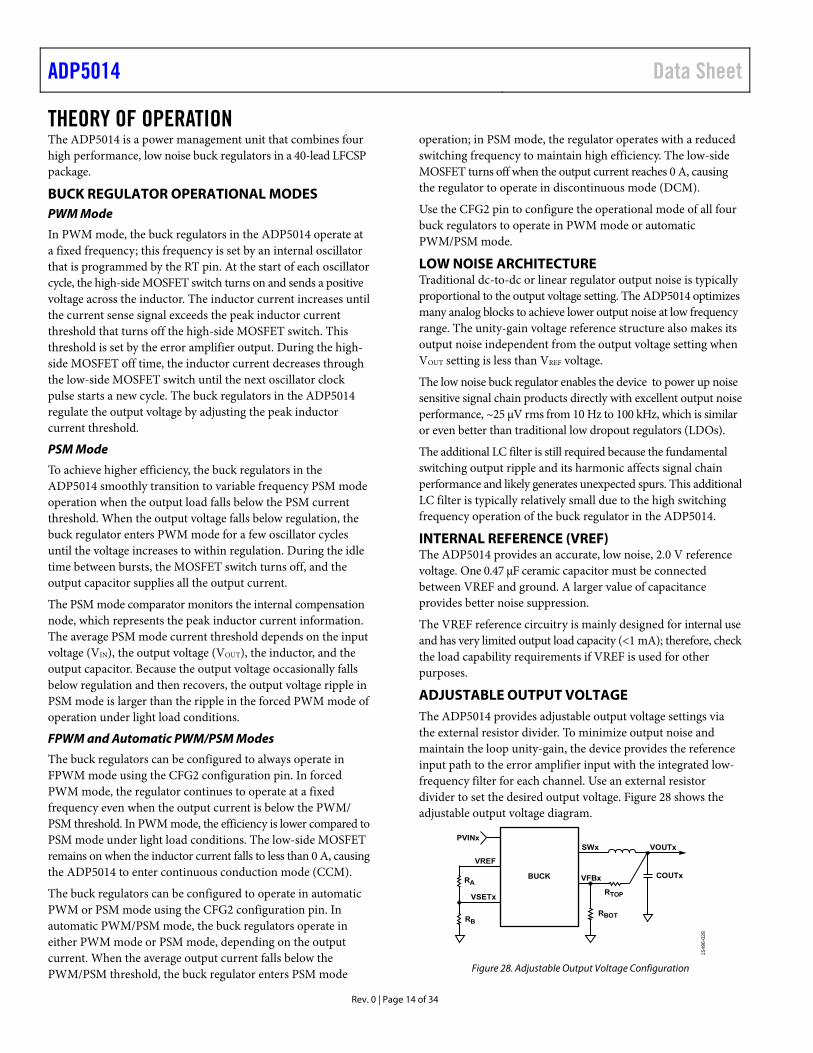
ADJUSTABLE OUTPUT VOLTAGE The ADP5014 provides adjustable output voltage settings via the external resistor divider. To minimize output noise and maintain the loop unity-gain, the device provides the reference input path to the error amplifier input with the integrated low-frequency filter for each channel. Use an external resistor divider to set the desired output voltage. Figure 28 shows the adjustable output voltage diagram.
BUCK COUTxRA
RB
VSETx
SWxPVINx
VREF
VFBx
VOUTx
RTOP
RBOT
1549
6-02
8
Figure 28. Adjustable Output Voltage Configuration
Data Sheet ADP5014
Rev. 0 | Page 15 of 34
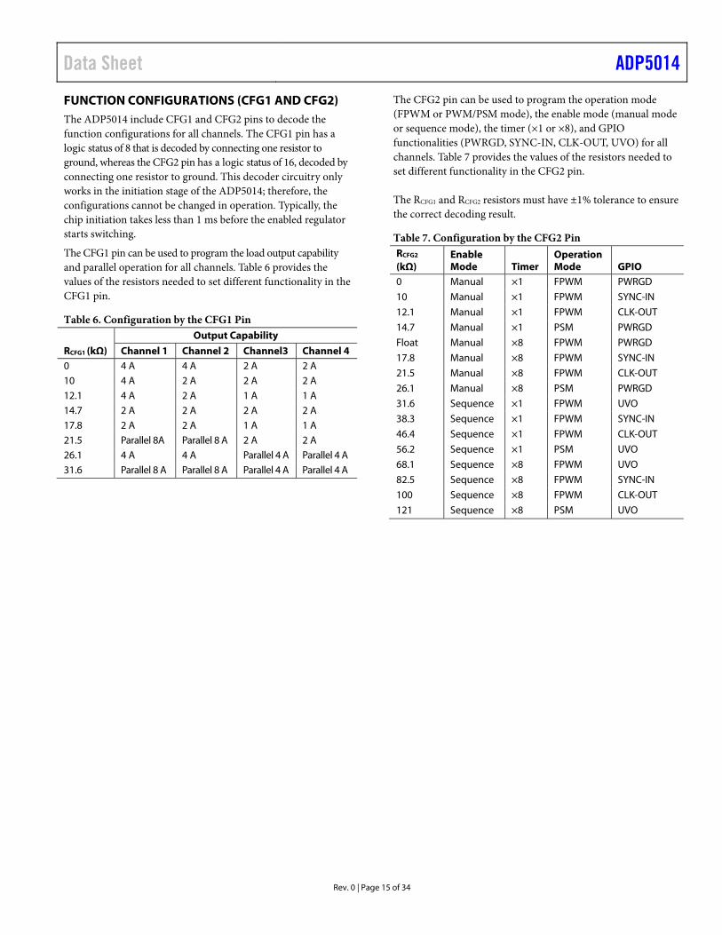
FUNCTION CONFIGURATIONS (CFG1 AND CFG2) The ADP5014 include CFG1 and CFG2 pins to decode the function configurations for all channels. The CFG1 pin has a logic status of 8 that is decoded by connecting one resistor to ground, whereas the CFG2 pin has a logic status of 16, decoded by connecting one resistor to ground. This decoder circuitry only works in the initiation stage of the ADP5014; therefore, the configurations cannot be changed in operation. Typically, the chip initiation takes less than 1 ms before the enabled regulator starts switching.
The CFG1 pin can be used to program the load output capability and parallel operation for all channels. Table 6 provides the values of the resistors needed to set different functionality in the CFG1 pin.
Table 6. Configuration by the CFG1 Pin
RCFG1 (kΩ)
Output Capability
Channel 1 Channel 2 Channel3 Channel 4 0 4 A 4 A 2 A 2 A 10 4 A 2 A 2 A 2 A 12.1 4 A 2 A 1 A 1 A 14.7 2 A 2 A 2 A 2 A 17.8 2 A 2 A 1 A 1 A 21.5 Parallel 8A Parallel 8 A 2 A 2 A 26.1 4 A 4 A Parallel 4 A Parallel 4 A 31.6 Parallel 8 A Parallel 8 A Parallel 4 A Parallel 4 A
The CFG2 pin can be used to program the operation mode (FPWM or PWM/PSM mode), the enable mode (manual mode or sequence mode), the timer (×1 or ×8), and GPIO functionalities (PWRGD, SYNC-IN, CLK-OUT, UVO) for all channels. Table 7 provides the values of the resistors needed to set different functionality in the CFG2 pin.
The RCFG1 and RCFG2 resistors must have ±1% tolerance to ensure the correct decoding result.
Table 7. Configuration by the CFG2 Pin RCFG2
(kΩ) Enable Mode Timer
Operation Mode GPIO
0 Manual ×1 FPWM PWRGD
10 Manual ×1 FPWM SYNC-IN
12.1 Manual ×1 FPWM CLK-OUT
14.7 Manual ×1 PSM PWRGD
Float Manual ×8 FPWM PWRGD
17.8 Manual ×8 FPWM SYNC-IN
21.5 Manual ×8 FPWM CLK-OUT
26.1 Manual ×8 PSM PWRGD
31.6 Sequence ×1 FPWM UVO
38.3 Sequence ×1 FPWM SYNC-IN
46.4 Sequence ×1 FPWM CLK-OUT
56.2 Sequence ×1 PSM UVO
68.1 Sequence ×8 FPWM UVO
82.5 Sequence ×8 FPWM SYNC-IN
100 Sequence ×8 FPWM CLK-OUT
121 Sequence ×8 PSM UVO
ADP5014 Data Sheet
Rev. 0 | Page 16 of 34
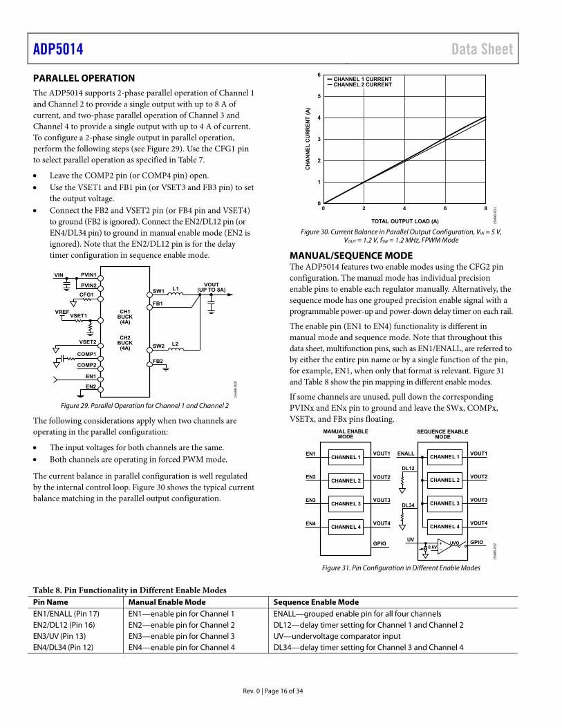
PARALLEL OPERATION The ADP5014 supports 2-phase parallel operation of Channel 1 and Channel 2 to provide a single output with up to 8 A of current, and two-phase parallel operation of Channel 3 and Channel 4 to provide a single output with up to 4 A of current. To configure a 2-phase single output in parallel operation, perform the following steps (see Figure 29). Use the CFG1 pin to select parallel operation as specified in Table 7.
Leave the COMP2 pin (or COMP4 pin) open. Use the VSET1 and FB1 pin (or VSET3 and FB3 pin) to set
the output voltage. Connect the FB2 and VSET2 pin (or FB4 pin and VSET4)
to ground (FB2 is ignored). Connect the EN2/DL12 pin (or EN4/DL34 pin) to ground in manual enable mode (EN2 is ignored). Note that the EN2/DL12 pin is for the delay timer configuration in sequence enable mode.
CH1BUCK(4A)
CH2BUCK(4A)
FB1
PVIN1VIN
EN1
EN2
COMP1
VSET1
SW1 L1
FB2
SW2 L2
PVIN2
COMP2
VREF
VSET2
CFG1
VOUT(UP TO 8A)
1549
6-03
0
Figure 29. Parallel Operation for Channel 1 and Channel 2
The following considerations apply when two channels are operating in the parallel configuration:
The input voltages for both channels are the same. Both channels are operating in forced PWM mode.
The current balance in parallel configuration is well regulated by the internal control loop. Figure 30 shows the typical current balance matching in the parallel output configuration.
CH
AN
NE
L C
UR
RE
NT
(A
)
TOTAL OUTPUT LOAD (A)
0 2 4 6 8
CHANNEL 1 CURRENTCHANNEL 2 CURRENT
1549
6-03
1
Figure 30. Current Balance in Parallel Output Configuration, VIN = 5 V,
VOUT = 1.2 V, fSW = 1.2 MHz, FPWM Mode
MANUAL/SEQUENCE MODE The ADP5014 features two enable modes using the CFG2 pin configuration. The manual mode has individual precision enable pins to enable each regulator manually. Alternatively, the sequence mode has one grouped precision enable signal with a programmable power-up and power-down delay timer on each rail.
The enable pin (EN1 to EN4) functionality is different in manual mode and sequence mode. Note that throughout this data sheet, multifunction pins, such as EN1/ENALL, are referred to by either the entire pin name or by a single function of the pin, for example, EN1, when only that format is relevant. Figure 31 and Table 8 show the pin mapping in different enable modes.
If some channels are unused, pull down the corresponding PVINx and ENx pin to ground and leave the SWx, COMPx, VSETx, and FBx pins floating.
CHANNEL 1
CHANNEL 2
CHANNEL 3
CHANNEL 4
VOUT1
VOUT2
VOUT3
VOUT4
EN1
EN2
EN3
EN4
GPIO
VOUT1
VOUT2
VOUT3
VOUT4
MANUAL ENABLEMODE
DL12
DL34
UV GPIO+–0.6V
SEQUENCE ENABLEMODE
ENALLCHANNEL 1
CHANNEL 2
CHANNEL 3
CHANNEL 4
1549
6-03
2
Figure 31. Pin Configuration in Different Enable Modes
Table 8. Pin Functionality in Different Enable Modes Pin Name Manual Enable Mode Sequence Enable Mode EN1/ENALL (Pin 17) EN1—enable pin for Channel 1 ENALL—grouped enable pin for all four channels EN2/DL12 (Pin 16) EN2—enable pin for Channel 2 DL12—delay timer setting for Channel 1 and Channel 2 EN3/UV (Pin 13) EN3—enable pin for Channel 3 UV—undervoltage comparator input EN4/DL34 (Pin 12) EN4—enable pin for Channel 4 DL34—delay timer setting for Channel 3 and Channel 4
Data Sheet ADP5014
Rev. 0 | Page 17 of 34
Manual Mode (Precision Enable)
In manual mode, the ADP5014 has an individual precision enable pin for each regulator. The enable control pin (ENx) features a precision enable circuit with a 0.6 V reference voltage. When the voltage at the ENx pin is greater than 0.6 V (typical), the regulator is enabled. When the ENx pin voltage falls below 0.57 V (typical), the regulator is disabled. To force the regulator to automatically start up when input power is applied, connect the enable pin to the input.
The precision enable pin has an internal pull-down current source (4 μA) that provides a default turn off when the enable pin is left open. When the enable pin exceeds 0.6 V (typical), the regulator is enabled and the internal pull-down current source at the enable pin decreases to 1 μA. The decrease in the current source allows the ratio of the external resistor divider to program the UVLO threshold to monitor either the input voltage or the output voltage while using the absolute value of external resistor divider to program the hysteresis window. Figure 32 shows the precision enable diagram.
0.6V
1µA 3µA
EN_CMP
+
–
RTOP_EN
RBOT_EN
1549
6-03
3
Figure 32. Precision Enable Diagram for One Channel
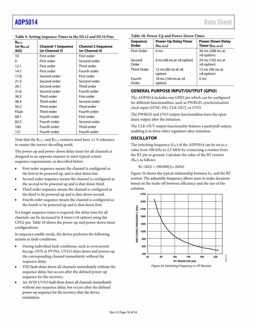
Sequence Mode
In sequence mode, all channels in the ADP5014 turn on and off under the control of the internal sequencer, which is triggered by the ENALL pin. The DL12 and DL34 pins set the predefined delay timer.
The ENALL pin features precision enable circuitry with a 0.6 V turn on threshold and internal pull-down current source. When the ENALL pin goes above the 0.6 V precision threshold, all channels controlled by the sequencer begin a soft start after the delay time specified by the DL12 and DL34 pin configuration. Similarly, when the ENALL pin falls below 0.57 V precision threshold, the channels turns off after the delay time specified by DL12 and DL34 pin configurations.
Figure 33 shows the logical states of each channel and does not show soft start and discharge ramps. Although the output discharge switch helps to discharge the output capacitor quickly, the discharge ramps on the output of each channel are still decided by many different factors, including the output capacitance, system load, and the ramps of input supply.
DL12 configures the delay timer for Channel 1 and Channel 2 by connecting one resistor to ground. Similarly, DL34 configures the delay timer for Channel 3 and Channel 4 (see Table 9). In parallel operation, the slave channel (Channel 2 or Channel 4) always follows up with the delay timer configuration of the master channel; therefore, Channel 2 follows Channel 1, while Channel 4 follows Channel 3. The delay timer decoder circuitry only works in the initiation stage of the ADP5014; therefore, the delay timer does not change in operation.
ENALL
tEN_DLY2
tEN_DLY1
tEN_DLY3
tEN_DLY4
tDIS_DLY1
tDIS_DLY2
tDIS_DLY3
tDIS_DLY4
ON
ON
ON
ON
OFF
OFF
OFF
OFF
CHANNEL1
CHANNEL2
CHANNEL3
CHANNEL4
1549
6-03
4
Figure 33. Power-Up/Power-Down in Sequence Enable Mode
ADP5014 Data Sheet
Rev. 0 | Page 18 of 34
Table 9. Setting Sequence Timer in the DL12 and DL34 Pins RDL12
(or RDL34) (kΩ)
Channel 1 Sequence (or Channel 3)
Channel 2 Sequence (or Channel 4)
10 First order First order 0 First order Second order 12.1 First order Third order 14.7 First order Fourth order 17.8 Second order First order 21.5 Second order Second order 26.1 Second order Third order 31.6 Second order Fourth order 38.3 Third order First order 46.4 Third order Second order 56.2 Third order Third order Float Third order Fourth order 68.1 Fourth order First order 82.5 Fourth order Second order 100 Fourth order Third order 121 Fourth order Fourth order
Note that the RDL12 and RDL34 resistors must have ±1 % tolerance to ensure the correct decoding result.
The power-up and power-down delay timer for all channels is designed in an opposite manner to meet typical system sequence requirements, as described below:
First order sequence means the channel is configured as the first to be powered up, and is shut down last.
Second order sequence means the channel is configured as the second to be powered up and is shut down third.
Third order sequence means the channel is configured as the third to be powered up and is shut down second.
Fourth order sequence means the channel is configured as the fourth to be powered up and is shut down first.
If a longer sequence timer is required, the delay time for all channels can be increased by 8 times (×8 option) using the CFG2 pin. Table 10 shows the power-up and power-down timer configurations.
In sequence enable mode, the device performs the following actions in fault conditions:
During individual fault conditions, such as overcurrent hiccup, OVP, or PVINx, UVLO shuts down and powers up the corresponding channel immediately without the sequence delay.
TSD fault shuts down all channels immediately without the sequence delay, but occurs after the defined power-up sequence for the recovery.
An AVIN UVLO fault shuts down all channels immediately without any sequence delay, but occurs after the defined power-up sequence for the recovery after the device reinitiation.
Table 10. Power-Up and Power-Down Timer Sequence Order
Power-Up Delay Timer (tEN_DLYx)
Power-Down Delay Timer (tDIS_DLYx)
First Order 0 ms 36 ms (288 ms at ×8 option)
Second Order
6 ms (48 ms at ×8 option) 24 ms (192 ms at ×8 option)
Third Order 12 ms (96 ms at ×8 option)
12 ms (96 ms at ×8 option)
Fourth Order
18 ms (144 ms at ×8 option)
0 ms
GENERAL PURPOSE INPUT/OUTPUT (GPIO) The ADP5014 includes one GPIO pin which can be configured for different functionalities, such as PWRGD, synchronization clock input (SYNC-IN), CLK-OUT, or UVO.
The PWRGD and UVO output functionalities have the open-drain output after the initiation.
The CLK-OUT output functionality features a push/pull output, enabling it to drive other regulators after initiation.
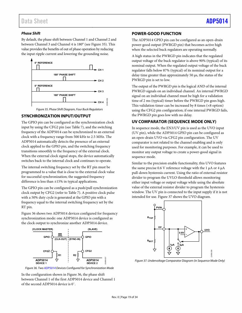
OSCILLATOR The switching frequency (fSW) of the ADP5014 can be set to a value from 500 kHz to 2.5 MHz by connecting a resistor from the RT pin to ground. Calculate the value of the RT resistor (RRT) as follows:
RRT (kΩ) = 100,000/fSW (kHz)
Figure 34 shows the typical relationship between fSW and the RT resistor. The adjustable frequency allows users to make decisions based on the trade-off between efficiency and the size of the solution.
2700
2400
2100
1800
1500
1200
900
600
30020 60 100 140
RT RESISTOR (kΩ)
SW
ITC
HIN
G F
RE
QU
EN
CY
(kH
z)
180 220
1549
6-03
5
Figure 34. Switching Frequency vs. RT Resistor
Data Sheet ADP5014
Rev. 0 | Page 19 of 34
Phase Shift
By default, the phase shift between Channel 1 and Channel 2 and between Channel 3 and Channel 4 is 180° (see Figure 35). This value provides the benefits of out of phase operation by reducing the input ripple current and lowering the grounding noise.
CH 2
CH 1
CH 3
CH 4
180° PHASE SHIFT
0° REFERENCE
180° PHASE SHIFT
0° REFERENCE
1549
6-03
6
Figure 35. Phase Shift Diagram, Four Buck Regulators
SYNCHRONIZATION INPUT/OUTPUT The GPIO pin can be configured as the synchronization clock input by using the CFG2 pin (see Table 7), and the switching frequency of the ADP5014 can be synchronized to an external clock with a frequency range from 500 kHz to 2.5 MHz. The ADP5014 automatically detects the presence of an external clock applied to the GPIO pin, and the switching frequency transitions smoothly to the frequency of the external clock. When the external clock signal stops, the device automatically switches back to the internal clock and continues to operate.
The internal switching frequency set by the RT pin must be programmed to a value that is close to the external clock value for successful synchronization; the suggested frequency difference is less than ±15% in typical applications.
The GPIO pin can be configured as a push/pull synchronization clock output by CFG2 (refer to Table 7). A positive clock pulse with a 50% duty cycle is generated at the GPIO pin with a frequency equal to the internal switching frequency set by the RT pin.
Figure 36 shows two ADP5014 devices configured for frequency synchronization mode: one ADP5014 device is configured as the clock output to synchronize another ADP5014 device.
GPIO GPIO
CFG
(CLOCK MASTER) (SLAVE)
ADP5014DEVICE 2
ADP5014DEVICE 1
(CLK-OUT) (SYNC-IN)
R1 R2
CFG2
1549
6-03
7
Figure 36. Two ADP5014 Devices Configured for Synchronization Mode
In the configuration shown in Figure 36, the phase shift between Channel 1 of the first ADP5014 device and Channel 1 of the second ADP5014 device is 0˚.
POWER-GOOD FUNCTION The ADP5014 GPIO pin can be configured as an open-drain power-good output (PWRGD pin) that becomes active high when the selected buck regulators are operating normally.
A high status in the PWRGD pin indicates that the regulated output voltage of the buck regulator is above 90% (typical) of its nominal output. When the regulated output voltage of the buck regulator falls below 87% (typical) of its nominal output for a delay time greater than approximately 50 μs, the status of the PWRGD pin is set to low.
The output of the PWRGD pin is the logical AND of the internal PWRGD signals on an individual channel. An internal PWRGD signal on an individual channel must be high for a validation time of 2 ms (typical) timer before the PWRGD pin goes high. This validation timer can be increased by 8 times (×8 option) using the CFG2 pin configuration; if one internal PWRGD fails, the PWRGD pin goes low with no delay.
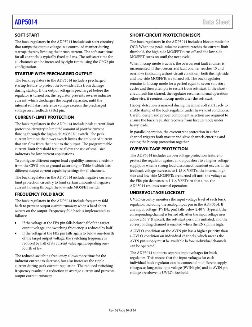
UV COMPARATOR (SEQUENCE MODE ONLY) In sequence mode, the EN3/UV pin is used as the UVO input (UV pin), while the ADP5014 GPIO pin can be configured as an open-drain UVO via CFG2 pin configuration. The UV comparator is not related to the channel enabling and is only used for monitoring purposes. For example, it can be used to monitor any output voltage to create a power-good signal in sequence mode.
Similar to the precision enable functionality, this UVO features the same precise 0.6 V reference voltage with the 1 μA or 4 μA pull-down hysteresis current. Using the ratio of external resistor divider to program the UVLO threshold allows monitoring either input voltage or output voltage while using the absolute value of the external resistor divider to program the hysteresis window. The UV pin is connected to the input supply if it is not intended for use. Figure 37 shows the UVO diagram.
0.6V
1µA 3µA
+
–
PVIN
UVUVO
RTOP
RBOT
1549
6-03
8
Figure 37. Undervoltage Comparator Diagram (in Sequence Mode Only)
ADP5014 Data Sheet
Rev. 0 | Page 20 of 34
SOFT START The buck regulators in the ADP5014 include soft start circuitry that ramps the output voltage in a controlled manner during startup, thereby limiting the inrush current. The soft start time for all channels is typically fixed at 2 ms. The soft start time for all channels can be increased by eight times using the CFG2 pin configuration.
STARTUP WITH PRECHARGED OUTPUT The buck regulators in the ADP5014 include a precharged startup feature to protect the low-side FETs from damage during startup. If the output voltage is precharged before the regulator is turned on, the regulator prevents reverse inductor current, which discharges the output capacitor, until the internal soft start reference voltage exceeds the precharged voltage on a feedback (FBx) pin.
CURRENT-LIMIT PROTECTION The buck regulators in the ADP5014 include peak current-limit protection circuitry to limit the amount of positive current flowing through the high-side MOSFET switch. The peak current limit on the power switch limits the amount of current that can flow from the input to the output. The programmable current-limit threshold feature allows the use of small size inductors for low current applications.
To configure different output load capability, connect a resistor from the CFG1 pin to ground according to Table 6 which lists different output current capability settings for all channels.
The buck regulators in the ADP5014 include negative current-limit protection circuitry to limit certain amounts of negative current flowing through the low-side MOSFET switch.
FREQUENCY FOLD BACK The buck regulators in the ADP5014 include frequency fold back to prevent output current runaway when a hard short occurs on the output. Frequency fold back is implemented as follows:
If the voltage at the FBx pin falls below half of the target output voltage, the switching frequency is reduced by half.
If the voltage at the FBx pin falls again to below one-fourth of the target output voltage, the switching frequency is reduced by half of its current value again, equaling one-fourth of fSW.
The reduced switching frequency allows more time for the inductor current to decrease, but also increases the ripple current during peak current regulation. The reduced switching frequency results in a reduction in average current and prevents output current runaway.
SHORT-CIRCUIT PROTECTION (SCP) The buck regulators in the ADP5014 include a hiccup mode for OCP. When the peak inductor current reaches the current-limit threshold, the high-side MOSFET turns off and the low-side MOSFET turns on until the next cycle.
When hiccup mode is active, the overcurrent fault counter is incremented. If the overcurrent fault counter reaches 15 and overflows (indicating a short-circuit condition), both the high-side and low-side MOSFETs are turned off. The buck regulator remains in hiccup mode for a period equal to seven soft start cycles and then attempts to restart from soft start. If the short-circuit fault has cleared, the regulator resumes normal operation; otherwise, it reenters hiccup mode after the soft start.
Hiccup detection is masked during the initial soft start cycle to enable startup of the buck regulator under heavy load conditions. Careful design and proper component selection are required to ensure the buck regulator recovers from hiccup mode under heavy loads.
In parallel operation, the overcurrent protection in either channel triggers both master and slave channels entering and exiting the hiccup protection together.
OVERVOLTAGE PROTECTION The ADP5014 includes an overvoltage protection feature to protect the regulator against an output short to a higher voltage supply, or when a strong load disconnect transient occurs. If the feedback voltage increases to 1.15 VSETx, the internal high-side and low-side MOSFETs are turned off until the voltage at the FBx pin decreases to 1.1 VSETx At that time, the ADP5014 resumes normal operation.
UNDERVOLTAGE LOCKOUT UVLO circuitry monitors the input voltage level of each buck regulator, including the analog input pin in the ADP5014. If any input voltage (PVINx pin) falls below 2.40 V (typical), the corresponding channel is turned off. After the input voltage rises above 2.65 V (typical), the soft start period is initiated, and the corresponding channel is enabled when the ENx pin is high.
A UVLO condition on the AVIN pin has a higher priority than a UVLO condition on individual channels, which means the AVIN pin supply must be available before individual channels can be operated.
The ADP5014 supports separate input voltages for buck regulators. This means that the input voltages for each individual buck regulator can be connected to different supply voltages, as long as its input voltage (PVINx pin) and its AVIN pin voltage are above its UVLO threshold.
Data Sheet ADP5014
Rev. 0 | Page 21 of 34
ACTIVE OUTPUT DISCHARGE SWITCH Each buck regulator in the ADP5014 integrates a discharge switch from the switching node to ground. This switch is turned on when its associated regulator is disabled, which helps discharge the output capacitor quickly. The typical value of the discharge switch is 85 Ω for Channel 1 to Channel 4.
THERMAL SHUTDOWN
If the ADP5014 junction temperature exceeds 150C, the thermal shutdown circuit turns off the IC except for the internal linear regulator. Extreme junction temperatures can be the result of high current operation, poor circuit board design, or high ambient temperature. A 15C hysteresis is included so that the ADP5014 does not return to operation after thermal shutdown until the on-chip temperature falls below 135C. When the device exits thermal shutdown, a soft start is initiated for each enabled channel.
ADP5014 Data Sheet
Rev. 0 | Page 22 of 34
APPLICATIONS INFORMATION ADIsimPOWER DESIGN TOOL The ADP5014 is supported by the ADIsimPower™ design tool set. ADIsimPower is a collection of tools that produce complete power designs optimized for a specific design goal. The tools enable the user to generate a full schematic and bill of materials and to calculate performance in minutes. ADIsimPower can optimize designs for cost, area, efficiency, and device count while considering the operating conditions and limitations of the IC and all real external components. The ADIsimPower tool can be found at http://www.analog.com/ADIsimPower; the user can request an unpopulated board through the tool.
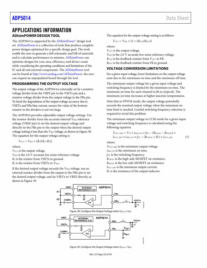
PROGRAMMING THE OUTPUT VOLTAGE The output voltage of the ADP5014 is externally set by a resistive voltage divider from the VREF pin to the VSETx pin and a resistive voltage divider from the output voltage to the FBx pin. To limit the degradation of the output voltage accuracy due to VSETx and FBx bias current, ensure the value of the bottom resistor in the dividers is not too large.
The ADP5014 provides adjustable output voltage settings. Use the resistor divider from the accurate internal VREF reference voltage (VREF pin) to set the desired output voltage and directly tie the FBx pin to the output when the desired output voltage setting is less than the VREF voltage, as shown in Figure 38. The equation for the output voltage setting is
VOUT = VREF × (R2/(R1+R2))
where: VOUT is the output voltage. VREF is the 2.0 V accurate low noise reference voltage. R2 is the resistor from VSETx to ground. R1 is the resistor from VSETx to VREF.
If the desired output voltage exceeds the VREF voltage, use an external resistor divider from the output to the FBx pin to set the desired output voltage, and tie VSETx to VREF directly, as shown in Figure 39.
The equation for the output voltage setting is as follows:
VOUT = VREF × (1 + (RTOP/RBOT))
where: VOUT is the output voltage. VREF is the 2.0 V accurate low noise reference voltage. RTOP is the feedback resistor from VOUT to FB. RBOT is the feedback resistor from FB to ground.
VOLTAGE CONVERSION LIMITATIONS For a given input voltage, lower limitations on the output voltage exist due to the minimum on time and the minimum off time.
The minimum output voltage for a given input voltage and switching frequency is limited by the minimum on time. The minimum on time for each channel is 60 ns (typical). The minimum on time increases at higher junction temperatures.
Note that in FPWM mode, the output voltage potentially exceeds the nominal output voltage when the minimum on time limit is reached. Careful switching frequency selection is required to avoid this problem.
The minimum output voltage in CCM mode for a given input voltage and switching frequency is calculated using the following equation:
VOUT_MIN = VIN × tMIN_ON × fSW − (RDSON1 − RDSON2) × IOUT_MIN × tMIN_ON × fSW − (RDSON2 + RL) × IOUT_MIN (1)
where: VOUT_MIN is the minimum output voltage. tMIN_ON is the minimum on time. fSW is the switching frequency. RDSON1 is the high-side MOSFET on resistance. RDSON2 is the low-side MOSFET on resistance. IOUT_MIN is the minimum output current. RL is the resistance of the output inductor.
+EA
VSETxR1
R2
ADP5014
FBx
SWx L
C
VOUTxCOMPx
VREF
–
INTERNALREFERENCE 2.0V
1549
6-03
9
Figure 38. Configure the Output Voltage when VOUTx ≤ VREF
+
–EA
INTERNALREFERENCE 2.0V
VSETx
ADP5014
FBx
SWx L
C
VOUTx
COMPx
VREF
RTOP
RBOT
1549
6-04
0
Figure 39. Configure the Output Voltage when VOUTX > VREF
Data Sheet ADP5014
Rev. 0 | Page 23 of 34
The maximum output voltage for a given input voltage and switching frequency is limited by the minimum off time or the maximum duty cycle. The minimum off time for each channel is 50 ns (typical).
The maximum output voltage for a given input voltage and switching frequency is calculated using the following equation:
VOUT_MAX = VIN × (1 − tMIN_OFF × fSW) − (RDSON1 − RDSON2) × IOUT_MAX × (1 − tMIN_OFF × fSW) − (RDSON2 + RL) × IOUT_MAX (2)
where: VOUT_MAX is the maximum output voltage. tMIN_OFF is the minimum off time. fSW is the switching frequency. RDSON1 is the high-side MOSFET on resistance. RDSON2 is the low-side MOSFET on resistance. IOUT_MAX is the maximum output current. RL is the resistance of the output inductor.
As shown in Equation 1 and Equation 2, reducing the switching frequency eases the minimum on time and off time limitations.
CURRENT-LIMIT SETTING The ADP5014 has two selectable current-limit thresholds for each channel. Ensure that the selected current-limit value is larger than the peak current of the inductor, IPEAK. See Table 6 for the current-limit configuration for each channel.
SOFT START SETTING The buck regulators in the ADP5014 include soft start circuitry that ramps the output voltage in a controlled manner during startup, thereby limiting the inrush current. To set the soft start time to a value of 2 ms or 16 ms, connect a resistor from the CFG2 pin to the ground (see the Soft Start section).
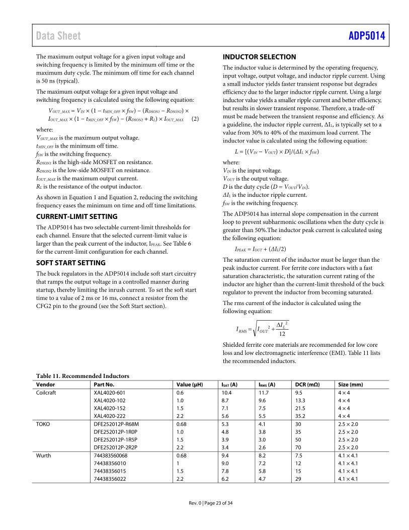
INDUCTOR SELECTION The inductor value is determined by the operating frequency, input voltage, output voltage, and inductor ripple current. Using a small inductor yields faster transient response but degrades efficiency due to the larger inductor ripple current. Using a large inductor value yields a smaller ripple current and better efficiency, but results in slower transient response. Therefore, a trade-off must be made between the transient response and efficiency. As a guideline, the inductor ripple current, ΔIL, is typically set to a value from 30% to 40% of the maximum load current. The inductor value is calculated using the following equation:
L = [(VIN − VOUT) × D]/(ΔIL × fSW)
where: VIN is the input voltage. VOUT is the output voltage. D is the duty cycle (D = VOUT/VIN). ΔIL is the inductor ripple current. fSW is the switching frequency.
The ADP5014 has internal slope compensation in the current loop to prevent subharmonic oscillations when the duty cycle is greater than 50%.The inductor peak current is calculated using the following equation:
IPEAK = IOUT + (ΔIL/2)
The saturation current of the inductor must be larger than the peak inductor current. For ferrite core inductors with a fast saturation characteristic, the saturation current rating of the inductor are higher than the current-limit threshold of the buck regulator to prevent the inductor from becoming saturated.
The rms current of the inductor is calculated using the following equation:
12
22 L
OUTRMSI
II
Shielded ferrite core materials are recommended for low core loss and low electromagnetic interference (EMI). Table 11 lists the recommended inductors.
Table 11. Recommended Inductors Vendor Part No. Value (μH) ISAT (A) IRMS (A) DCR (mΩ) Size (mm) Coilcraft XAL4020-601 0.6 10.4 11.7 9.5 4 × 4
XAL4020-102 1.0 8.7 9.6 13.3 4 × 4 XAL4020-152 1.5 7.1 7.5 21.5 4 × 4 XAL4020-222 2.2 5.6 5.5 35.2 4 × 4
TOKO DFE252012P-R68M 0.68 5.3 4.1 30 2.5 × 2.0 DFE252012P-1R0P 1.0 4.8 3.8 35 2.5 × 2.0 DFE252012P-1R5P 1.5 3.9 3.0 50 2.5 × 2.0 DFE252012P-2R2P 2.2 3.4 2.6 70 2.5 × 2.0
Wurth 744383560068 0.68 9.4 8.2 7.5 4.1 × 4.1 74438356010 1 9.0 7.2 12 4.1 × 4.1 74438356015 1.5 7.8 5.8 15 4.1 × 4.1 74438356022 2.2 6.2 4.7 29 4.1 × 4.1
ADP5014 Data Sheet
Rev. 0 | Page 24 of 34
OUTPUT CAPACITOR SELECTION The selected output capacitor affects both the output voltage ripple and the loop dynamics of the regulator. For example, during load step transients on the output, when the load is suddenly increased, the output capacitor supplies the load until the control loop can ramp up the inductor current, causing an undershoot of the output voltage.
The output capacitance required to meet the voltage droop requirement (COUT_UV) is calculated using the following equation:
UVOUTOUTIN
STEPUVUVOUT
VVV
LIKC
_
2
_2
where: KUV is a factor (typically set to 2). ΔISTEP is the load step. ΔVOUT_UV is the allowable undershoot on the output voltage.
Another example of the effect of the output capacitor on the loop dynamics of the regulator is when the load is suddenly removed from the output. The energy stored in the inductor rushes into the output capacitor, causing an overshoot of the output voltage.
The output capacitance required to meet the overshoot requirement (COUT_UV) is calculated using the following equation:
22
2
_OUTOUT_OVOUT
STEPOVOVOUT
VVV
LIKC
where: KOV is a factor (typically set to 2). ΔISTEP is the load step. ΔVOUT_OV is the allowable overshoot on the output voltage.
The output voltage ripple is determined by the equivalent series resistance (ESR) of the output capacitor and its capacitance value. Use the following equation to select a capacitor that can meet the output ripple requirements:
RIPPLEOUTSW
LRIPPLEOUT
Vf
IC
__
8
L
RIPPLEOUTESR
I
VR
_
where: ΔVOUT_RIPPLE is the allowable output voltage ripple. RESR is the ESR of the output capacitor.
Select the largest output capacitance given by COUT_UV, COUT_OV, and COUT_RIPPLE to meet both load transient and output ripple requirements.
The selected output capacitor voltage rating must be greater than the output voltage. The minimum rms current rating of the output capacitor (ICOUT_rms) is determined by the following equation:
ICOUT_rms = 12LI
INPUT CAPACITOR SELECTION The input decoupling capacitor attenuates high frequency noise on the input and acts as an energy reservoir. This capacitor is a ceramic capacitor and must be placed close to the PVINx pins. The loop composed of the input capacitor, the high-side MOSFET, and the low-side MOSFET must be kept as small as possible. The voltage rating of the input capacitor must be greater than the maximum input voltage. The rms current rating of the input capacitor (ICIN_rms)is larger than the following equation:
ICIN_rms = IOUT × )1( DD
where D is the duty cycle (D = VOUT/VIN).
PROGRAMMING THE UVLO INPUT The precision enable input can be used to program the UVLO threshold of the input voltage, as shown in Figure 32
The precision turn on threshold is 0.6 V. Use the following equations to calculate RTOP_EN and RBOT_EN:
RTOP_EN = (0.57 V × VIN_RISING − 0.6 × VIN_FALLING)/(0.57 V × 4 μA − 0.6 × 1 μA)
RBOT_EN = (0.6 V × RTOP_EN)/(VIN_RISING – RTOP_EN × 4 μA − 0.6 V)
where: RTOP_EN is the resistor from PVINx to ENx. VIN_RISING is the VIN rising threshold. VIN_FALLING is the VIN falling threshold. RBOT_EN is the resistor from ENx to ground.
COMPENSATION COMPONENTS DESIGN For the peak current-mode control architecture, the power stage can be simplified as a voltage controlled current source that supplies current to the output capacitor and load resistor. The simplified loop is composed of one domain pole and a zero contributed by the ESR of the output capacitor. The control to output transfer function (Gvd) is shown in the following equations:
p
zVI
COMP
OUTvd
fs
fs
RAsV
sVG
21
21
)()(
)s(
OUTESRz
CRf
2
1
OUTESRp
CRRf
2
1
where: AVI = 16.67A/V for Channel 1 or Channel 2, and 8.33 A/V for Channel 3 or Channel 4. R is the load resistance. fz is the frequency of the zero. COUT is the output capacitance. RESR is the equivalent series resistance of the output capacitor. fp is the frequency of the pole.
Data Sheet ADP5014
Rev. 0 | Page 25 of 34
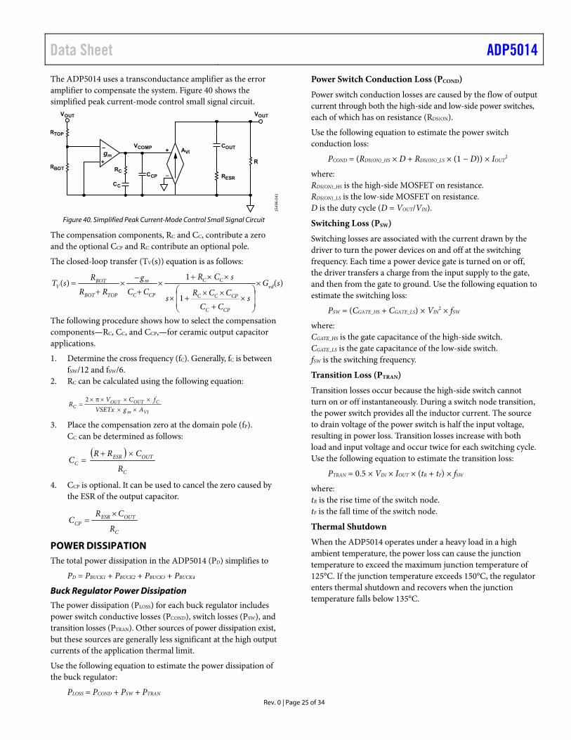
The ADP5014 uses a transconductance amplifier as the error amplifier to compensate the system. Figure 40 shows the simplified peak current-mode control small signal circuit.
RESR
R
+
–
gm
RCCCP
COUT
CC
RTOP
RBOT
–
+
AVI
VOUT
VCOMP
VOUT
1549
6-04
1
Figure 40. Simplified Peak Current-Mode Control Small Signal Circuit
The compensation components, RC and CC, contribute a zero and the optional CCP and RC contribute an optional pole.
The closed-loop transfer (TV(s)) equation is as follows:
)(
1
1)( sG
sCC
CCRs
sCR
CC
g
RR
RsT vd
CPC
CPCC
CC
CPC
m
TOPBOT
BOTV
The following procedure shows how to select the compensation components—RC, CC, and CCP,—for ceramic output capacitor applications.
1. Determine the cross frequency (fC). Generally, fC is between fSW/12 and fSW/6.
2. RC can be calculated using the following equation:
VIm
COUTOUTC AgVSETx
fCVR
2
3. Place the compensation zero at the domain pole (fP). CC can be determined as follows:
C
OUTESRC
R
CRRC
4. CCP is optional. It can be used to cancel the zero caused by the ESR of the output capacitor.
C
OUTESRCP
R
CRC
POWER DISSIPATION The total power dissipation in the ADP5014 (PD) simplifies to
PD = PBUCK1 + PBUCK2 + PBUCK3 + PBUCK4
Buck Regulator Power Dissipation
The power dissipation (PLOSS) for each buck regulator includes power switch conductive losses (PCOND), switch losses (PSW), and transition losses (PTRAN). Other sources of power dissipation exist, but these sources are generally less significant at the high output currents of the application thermal limit.
Use the following equation to estimate the power dissipation of the buck regulator:
PLOSS = PCOND + PSW + PTRAN
Power Switch Conduction Loss (PCOND)
Power switch conduction losses are caused by the flow of output current through both the high-side and low-side power switches, each of which has on resistance (RDS(ON).
Use the following equation to estimate the power switch conduction loss:
PCOND = (RDS(ON)_HS × D + RDS(ON)_LS × (1 − D)) × IOUT2
where: RDS(ON)_HS is the high-side MOSFET on resistance. RDS(ON)_LS is the low-side MOSFET on resistance. D is the duty cycle (D = VOUT/VIN).
Switching Loss (PSW)
Switching losses are associated with the current drawn by the driver to turn the power devices on and off at the switching frequency. Each time a power device gate is turned on or off, the driver transfers a charge from the input supply to the gate, and then from the gate to ground. Use the following equation to estimate the switching loss:
PSW = (CGATE_HS + CGATE_LS) × VIN2 × fSW
where: CGATE_HS is the gate capacitance of the high-side switch. CGATE_LS is the gate capacitance of the low-side switch. fSW is the switching frequency.
Transition Loss (PTRAN)
Transition losses occur because the high-side switch cannot turn on or off instantaneously. During a switch node transition, the power switch provides all the inductor current. The source to drain voltage of the power switch is half the input voltage, resulting in power loss. Transition losses increase with both load and input voltage and occur twice for each switching cycle. Use the following equation to estimate the transition loss:
PTRAN = 0.5 × VIN × IOUT × (tR + tF) × fSW
where: tR is the rise time of the switch node. tF is the fall time of the switch node.
Thermal Shutdown
When the ADP5014 operates under a heavy load in a high ambient temperature, the power loss can cause the junction temperature to exceed the maximum junction temperature of 125°C. If the junction temperature exceeds 150°C, the regulator enters thermal shutdown and recovers when the junction temperature falls below 135°C.
ADP5014 Data Sheet
Rev. 0 | Page 26 of 34
JUNCTION TEMPERATURE The junction temperature of the die is the sum of the ambient temperature of the environment and the temperature rise of the package due to power dissipation, as shown in the following equation:
TJ = TA + TR
where: TJ is the junction temperature. TA is the ambient temperature. TR is the rise in temperature of the package due to power dissipation.
The rise in temperature of the package is directly proportional to the power dissipation in the package. The proportionality constant for this relationship is the thermal resistance from the junction of the die to the ambient temperature, as shown in the following equation:
TR = θJA × PD
where: TR is the rise in temperature of the package. θJA is the thermal resistance from the junction of the die to the ambient temperature of the package (see Table 4). Thermal
performance is directly linked to PCB design and operating environment. Careful attention to PCB thermal design is required. PD is the power dissipation in the package.An important factor to consider is that the thermal resistance value is based on a 4-layer, 4 inch × 3 inch PCB with 2.5 oz of copper, as specified in the JEDEC standard, whereas real world applications can use PCBs with different dimensions and a different number of layers.
It is important to maximize the amount of copper used to remove heat from the device. Copper exposed to air dissipates heat better than copper used in the inner layers. The exposed pad is connected to the ground plane with several vias.
Data Sheet ADP5014
Rev. 0 | Page 27 of 34
DESIGN EXAMPLES This section provides an example of the step by step design procedures and the external components required for Channel 1. Table 12 lists the design requirements for this example.
Table 12. Example Design Requirements for Channel 1 Parameter Specification Input Voltage VPVIN1 = 5 V ± 5% Output Voltage VOUT1 = 1.2 V Output Current IOUT1 = 4 A Output Ripple ΔVOUT1_RIPPLE = 5 mV in CCM mode Load Transient ±5%, at 20% to 80% load transient, 1 A/μs
Although this example shows step by step design procedures for Channel 1, the procedures apply to all other buck regulator channels (Channel 2 to Channel 4).
SETTING THE SWITCHING FREQUENCY The first step when setting the switching frequency is to determine the switching frequency for the ADP5014 design. In general, higher switching frequencies produce a smaller solution size due to the lower component values required, whereas lower switching frequencies result in higher conversion efficiency due to lower switching losses.
The switching frequency of the ADP5014 can be set to a value from 500 kHz to 2.5 MHz by connecting a resistor from the RT pin to ground. The selected resistor allows users to make decisions based on the trade-off between efficiency and solution size. For more information, see the Oscillator section.
However, the highest supported switching frequency must be assessed by checking the voltage conversion limitations enforced by the minimum on time and the minimum off time (see the Voltage Conversion Limitations section).
In this design example, a switching frequency of 1.2 MHz achieves a good combination of small solution size and high conversion efficiency. To set the switching frequency to 1.2 MHz, use the following equation to calculate the resistor value, RRT:
RRT (kΩ) = (100,000/fSW (kHz))
According to this equation, select standard resistor RRT = 82.5 kΩ.
SETTING THE OUTPUT VOLTAGE Because the desired output voltage setting is less than VREF voltage, use the resistor divider from the accurate internal VREF reference voltage to set the desired output voltage and directly tie the feedback pin (FB1) to the output (see Figure 38). Select a 10 kΩ bottom resistor (R2) and then calculate the top resistor using the following equation:
R1 = R2 × ((VREF − VOUT)/VOUT)
where: VOUT is the output voltage. VREF is 2.0 V for Channel 1 to Channel 4.
To set the output voltage to 1.2 V, choose the following resistor values: R1 = 6.65 kΩ, and R2 = 10 kΩ.
SETTING THE CONFIGUATIONS (CFG1 AND CFG2) The CFG1 pin can be used to program the load output capability and parallel operation for all channels. For this example, choose RCFG1 = 0 kΩ. For more information, see the configuration in Function Configurations (CFG1 and CFG2).
The CFG2 pin can be used to program the operation mode (FPWM or PWM/PSM mode), the enable mode (manual mode or sequence mode), the timer (×1 or ×8), and GPIO functionalities (PWRGD, SYNC-IN, CLK-OUT, UVO) for all channels. For this example, choose RCFG2 = 0 kΩ. For more information, see the configuration in Function Configurations (CFG1 and CFG2).
SELECTING THE INDUCTOR The peak-to-peak inductor ripple current, ΔIL, is set to 30% of the maximum output current. Use the following equation to estimate the value of the inductor (L):
SWL
OUTIN
fI
DVVL
)(
where: VIN = 5 V. VOUT = 1.2 V. D is the duty cycle (D = VOUT/VIN = 0.24). ΔIL = 30% × 4 A = 1.2 A. fSW = 1.2 MHz.
The resulting value for L is 0.63 μH. The closest standard inductor value is 0.8 μH; therefore, the inductor ripple current, ΔIL1, is 0.95 A.
The inductor peak current is calculated using the following equation:
IPEAK = IOUT + (ΔIL/2)
The calculated peak current for the inductor is 4.48 A.
The rms current of the inductor can be calculated using the following equation:
12
22 L
OUTRMSI
II
The rms current of the inductor is approximately 4.01 A. Therefore, an inductor with a minimum rms current rating of 4.01 A and a minimum saturation current rating of 4.48 A is required. However, to prevent the inductor from reaching its saturation point in current-limit conditions, it is recommended that the inductor saturation current be higher than the maximum peak current limit, typically 6 A, for reliable operation.
Based on these requirements and recommendations, the COILCRAFT XAL5030-801MEB, with a direct current resistance (DCR) of 5.14 mΩ, is selected for this design.
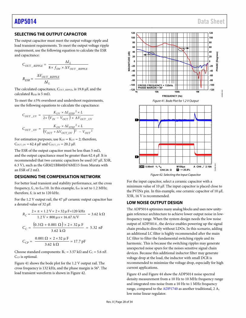
ADP5014 Data Sheet
Rev. 0 | Page 28 of 34
SELECTING THE OUTPUT CAPACITOR The output capacitor must meet the output voltage ripple and load transient requirements. To meet the output voltage ripple requirement, use the following equation to calculate the ESR and capacitance:
RIPPLEOUTSW
LRIPPLEOUT Vf
IC
__ 8
L
RIPPLEOUTESR I
VR
_
The calculated capacitance, COUT_RIPPLE, is 19.8 μF, and the calculated RESR is 5 mΩ.
To meet the ±5% overshoot and undershoot requirements, use the following equations to calculate the capacitance:
UVOUTOUTIN
STEPUVUVOUT VVV
LIKC
_
2
_ 2
22
2
_OUTOUT_OVOUT
STEPOVOVOUT VVV
LIKC
For estimation purposes, use KOV = KUV = 2; therefore, COUT_OV = 62.4 μF and COUT_UV = 20.2 μF.
The ESR of the output capacitor must be less than 5 mΩ, and the output capacitance must be greater than 62.4 μF. It is recommended that two ceramic capacitors be used (47 μF, X5R, 6.3 V), such as the GRM21BR60J476ME15 from Murata with an ESR of 2 mΩ.
DESIGNING THE COMPENSATION NETWORK For better load transient and stability performance, set the cross frequency, fC, to fSW/10. In this example, fSW is set to 1.2 MHz; therefore, fC is set to 120 kHz.
For the 1.2 V output rail, the 47 μF ceramic output capacitor has a derated value of 32 μF.
k62.3
A/V67.16s800V2.1kHz120F322V2.12
CR
nF32.5
k62.3F322001.03.0
CC
pF7.17k62.3
F322001.0
CPC
Choose standard components: RC = 3.57 kΩ and CC = 5.6 nF. CCP is optional.
Figure 41 shows the bode plot for the 1.2 V output rail. The cross frequency is 132 kHz, and the phase margin is 56°. The load transient waveform is shown in Figure 42.
MA
GN
ITU
DE
(d
B)
PH
AS
E (
Deg
rees
)
120
100
80
60
40
20
0
–20
–40
–60
–80
–100
–120
120
100
80
60
40
20
0
–20
–40
–60
–80
–100
–1201k 10k 100k
FREQUENCY (Hz)
1M
CROSS FREQUENCY = 132kHzPHASE MARGIN = 56°
1549
6-04
2
Figure 41. Bode Plot for 1.2 V Output
CH1 5.00mVCH4 2A
M100µs A CH4 2.16A
1
4
T 25.8%Ω 1549
6-04
3
BW
Figure 42. Selecting the Input Capacitor
For the input capacitor, select a ceramic capacitor with a minimum value of 10 μF. The input capacitor is placed close to the PVINx pin. In this example, one ceramic capacitor of 10 μF, X5R, 16 V is recommended.
LOW NOISE OUTPUT DESIGN
The ADP5014 optimizes many analog blocks and uses new unity-gain reference architecture to achieve lower output noise in low-frequency range. When the system design needs the low noise output of ADP5014 , the device enables powering up the signal chain products directly without LDOs. In this scenario, adding an additional LC filter is highly recommended after the main LC filter to filter the fundamental switching ripple and its harmonic. This is because the switching ripples may generate unexpected noise spurs for the noises sensitive signal chain devices. Because this additional inductor filter may generate voltage drop at the load, the inductor with small DCR is recommended to minimize the voltage drop, especially for high current applications.
Figure 43 and Figure 44 show the ADP5014 noise spectral density measurement from a 10 Hz to 10 MHz frequency range and integrated rms noise from a 10 Hz to 1 MHz frequency range, compared to the ADP1740 as another traditional, 2 A, low noise linear regulator.
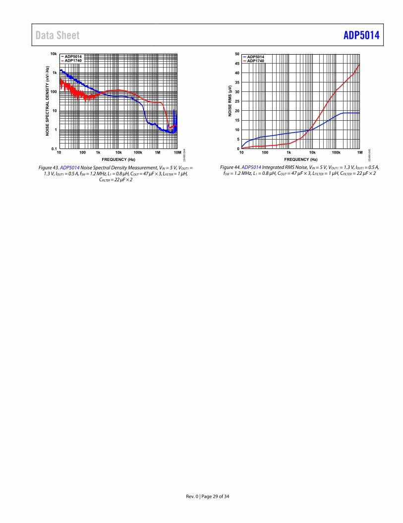
Data Sheet ADP5014
Rev. 0 | Page 29 of 34
FREQUENCY (Hz)
NO
ISE
SP
EC
TR
AL
DE
NS
ITY
(n
V/√
Hz)
10k
1k
100
10
1
0.110 100 1k 10k 100k 10M1M
ADP5014ADP1740
1549
6-04
4
Figure 43. ADP5014 Noise Spectral Density Measurement, VIN = 5 V, VOUT1 =
1.3 V, IOUT1 = 0.5 A, fSW = 1.2 MHz, L1 = 0.8 μH, COUT = 47 μF × 3, LFILTER = 1 μH, CFILTER = 22 μF × 2
FREQUENCY (Hz)
NO
ISE
RM
S (
µV
)
50
35
40
45
20
25
30
15
10
5
010 100 1k 10k 100k 1M
ADP5014ADP1740
1549
6-04
5
Figure 44. ADP5014 Integrated RMS Noise, VIN = 5 V, VOUT1 = 1.3 V, IOUT1 = 0.5 A,
fSW = 1.2 MHz, L1 = 0.8 μH, COUT = 47 μF × 3, LFILTER = 1 μH, CFILTER = 22 μF × 2
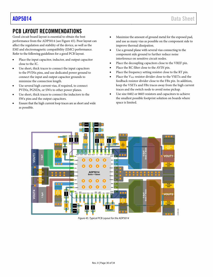
ADP5014 Data Sheet
Rev. 0 | Page 30 of 34
PCB LAYOUT RECOMMENDATIONS Good circuit board layout is essential to obtain the best performance from the ADP5014 (see Figure 45). Poor layout can affect the regulation and stability of the device, as well as the EMI and electromagnetic compatibility (EMC) performance. Refer to the following guidelines for a good PCB layout.
Place the input capacitor, inductor, and output capacitor close to the IC.
Use short, thick traces to connect the input capacitors to the PVINx pins, and use dedicated power ground to connect the input and output capacitor grounds to minimize the connection length.
Use several high current vias, if required, to connect PVINx, PGNDx, or SWx to other power planes.
Use short, thick traces to connect the inductors to the SWx pins and the output capacitors.
Ensure that the high current loop traces are as short and wide as possible.
Maximize the amount of ground metal for the exposed pad, and use as many vias as possible on the component side to improve thermal dissipation.
Use a ground plane with several vias connecting to the component side ground to further reduce noise interference on sensitive circuit nodes.
Place the decoupling capacitors close to the VREF pin. Place the RC filter close to the AVIN pin. Place the frequency setting resistor close to the RT pin. Place the VREF resistor divider close to the VSETx and the
feedback resistor divider close to the FBx pin. In addition, keep the VSETx and FBx traces away from the high current traces and the switch node to avoid noise pickup.
Use size 0402 or 0603 resistors and capacitors to achieve the smallest possible footprint solution on boards where space is limited.
VO
UT
3V
OU
T4
1.5µ
H1.
5µH
47µF6.3V/XR5
0603
47µF6.3V/XR5
0603
VOUT1
VOUT2
47µF6.3V/XR5
0805
47µF6.3V/XR5
0805
47µF6.5V/XR5
0805
47µF6.3V/XR5
0805
0.8µ
H4m
m ×
4m
m0.
8µH
4mm
× 4
mm
10
µF
6.3
V/X
R5
06
03
10µ
F6.
3V
/XR
506
03
R0
40
2
R0
40
2
C0
40
2
R0402 R0402
R0402
R0
40
2
R0
40
2
R0
40
2R
04
02
R0402
0.1
µF
6.3
V/X
R5
04
02
0.1
µF
6.3
V/X
R5
04
02
10µ
F6.
3V
/XR
506
03
10
µF6
.3V
/XR
506
03
R0
40
2C
04
02
R0
40
2
R0
40
2
R0
40
2
C0
40
2
R0402
R0402
ADP50146mm × 6mm
30
29
28
27
26
25
24
23
22
21
40
39
38
37
36
35
34
33
32
31
11
12
13
14
15
16
17
18
19
20
VSET4
FB3
FB4
VSET3 VREF VSET2 VSET1 RT AVIN FB1 COMP1
PVIN1
PVIN1
SW1
PVIN2GPIOEN4/DL34 EN3/UV CFG2 CFG1
EN2/DL12
EN1/ENALL FB2 COMP2
COMP3
PVIN3
SW3
PGND3
PGND4
SW4
PVIN4
COMP4
SW1
PGND1
PGND1
PGND2
PGND2
SW2
SW2
PVIN2
1
2
3
4
5
6
7
8
9
10
1549
6-04
6
Figure 45. Typical PCB Layout for the ADP5014
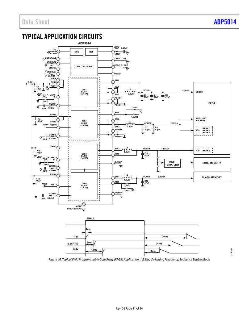
Data Sheet ADP5014
Rev. 0 | Page 31 of 34
TYPICAL APPLICATION CIRCUITS
1.5µH
10nF
L1
GPIO
AVINFB1
SW1
SW1
L3SW3
FB3
PGND3
L4SW4
FB4
PGND4
PVIN1
PVIN1
PVIN2
PVIN2
PVIN3
COMP3
PVIN4
5.0V
VOUT1
VOUT3
VOUT4
AGNDEXPOSED PAD
ADP5014
PGND1
PGND1
L2
FB2
SW2
SW2
VOUT2
PGND2
EN3/UV
EN2/DL12
EN1/ENALL
EN4/DL34
VREF
CFG1
CFG2
RTREFOSC
LOGIC DECODER
C347µF
1.2V/4A
2.5V/2A
1.5V/2A
3.3V/2A
0.47µF
0Ω
0.8µH
0.8µH
1.5µH
C747µF
C1047µF
C1247µF
4.32kΩ
C110µF
C21µF
10nF
13.3kΩ
COMP1
VSET1VREF
20kΩ
4.32kΩ
10nF
COMP2
VSET2VREF
4.32kΩ
10nF
COMP4
VSET4VREF
6.65kΩ VSET3VREF
20kΩ
6.04kΩ
CH 1BUCK
(2A/4A)
CH 2BUCK
(2A/4A)
CH 3BUCK
(1A/2A)
CH 4BUCK
(1A/2A)
C447µF
C847µF
82.5kΩ
C610µF
C910µF
C1110µF
VCORE
AUXILIARYVOLTAGE
FPGA
VREF
ENALL
2ms
6ms
12ms
24ms
36ms
12ms
C547µF
31.6kΩ
4.99kΩ
20kΩ
0Ω
26.1kΩ
1.2V
2.5V/1.5V
3.3V
I/OsBANK 0BANK 1BANK 2
I/Os BANK 3
1549
6-04
7
PGND2
13kΩ
20kΩ
DDRTERM. LDO
DDR3 MEMORY
FLASH MEMORY
Figure 46. Typical Field Programmable Gate Array (FPGA) Application, 1.2 MHz Switching Frequency, Sequence Enable Mode
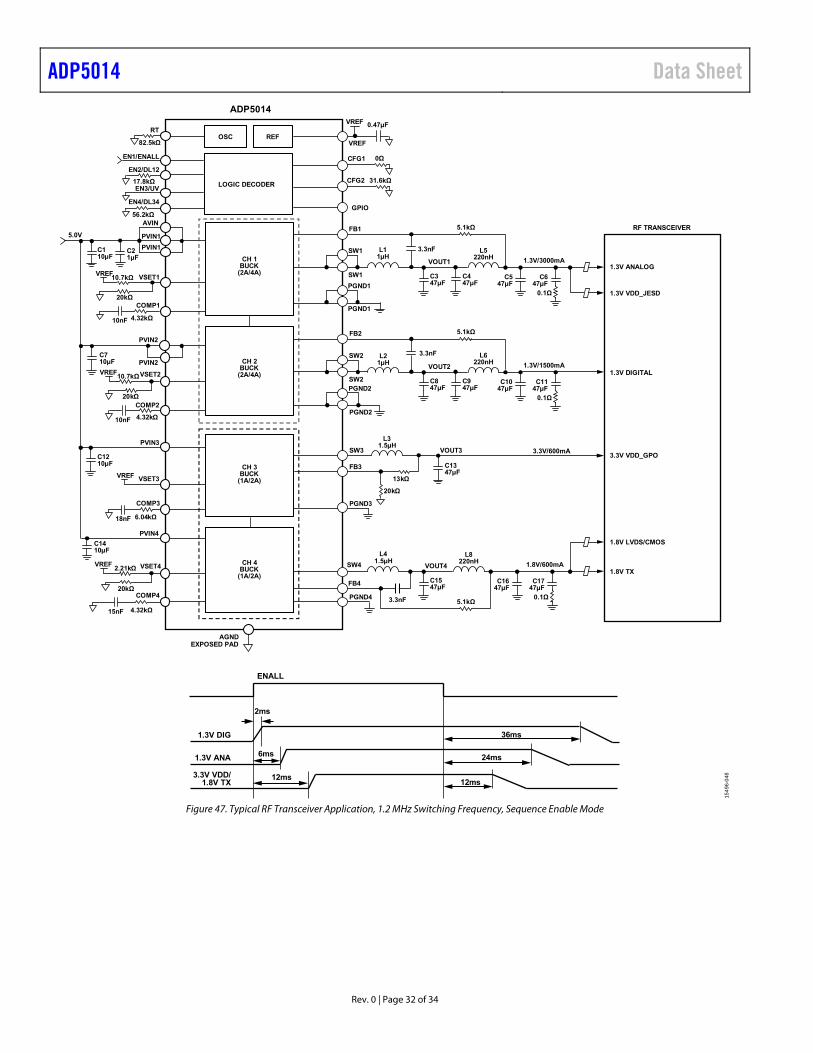
ADP5014 Data Sheet
Rev. 0 | Page 32 of 34
18nF
13kΩ
L1
GPIO
AVINFB1
SW1
SW1
L3
SW3
FB3
PGND3
SW4
PGND4
PVIN1
PVIN1
PVIN2
PVIN2
PVIN3
COMP3
PVIN4
5.0V
VOUT1
VOUT3
AGNDEXPOSED PAD
ADP5014
PGND1
PGND1
FB2
SW2
SW2PGND2
EN3/UV
EN2/DL12
VSET3
EN1/ENALL
EN4/DL34
VREF
VREF
CFG1
CFG2
RTREFOSC
LOGIC DECODER
C347µF
1.3V/3000mA
0.47µF
0Ω
1µH
1.5µH
C1347µF
20kΩ
6.04kΩ
C110µF
C21µF
10nF
10.7kΩ
COMP1
VSET1VREF
20kΩ
4.32kΩ
10nF
10.7kΩ
COMP2
VSET2VREF
20kΩ
4.32kΩ
15nF
2.21kΩ
COMP4
VSET4VREF
20kΩ
4.32kΩ
CH 1BUCK
(2A/4A)
CH 2BUCK
(2A/4A)
CH 3BUCK
(1A/2A)
CH 4BUCK
(1A/2A)
C447µF
5.1kΩ
82.5kΩ
C710µF
C1210µF
C1410µF
1.3V ANALOG
RF TRANSCEIVER
3.3V/600mA
VREF
ENALL
2ms
6ms
12ms
24ms
36ms
12ms
C547µF
3.3nF L5220nH
C647µF
0.1Ω
31.6kΩ17.8kΩ
56.2kΩ
1.3V DIG
1.3V ANA
3.3V VDD/1.8V TX
1.3V DIGITAL
1.3V VDD_JESD
3.3V VDD_GPO
1.8V LVDS/CMOS
1.8V TX
1549
6-04
8
PGND2
L4
FB4
VOUT4
C1547µF
1.8V/600mA1.5µH
5.1kΩ
C1647µF
3.3nF
L8220nH
C1747µF
0.1Ω
L2
VOUT2
C847µF
1.3V/1500mA1µH
C947µF
5.1kΩ
C1047µF
3.3nF L6220nH
C1147µF
0.1Ω
Figure 47. Typical RF Transceiver Application, 1.2 MHz Switching Frequency, Sequence Enable Mode
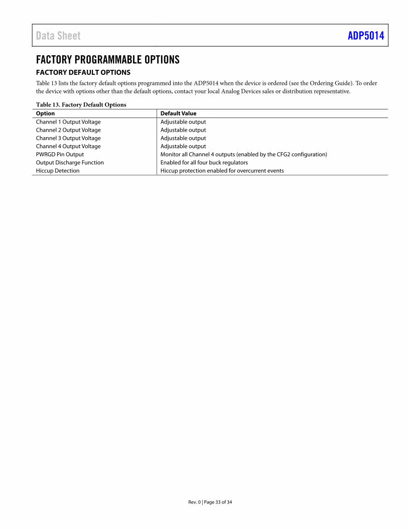
Data Sheet ADP5014
Rev. 0 | Page 33 of 34
FACTORY PROGRAMMABLE OPTIONS FACTORY DEFAULT OPTIONS Table 13 lists the factory default options programmed into the ADP5014 when the device is ordered (see the Ordering Guide). To order the device with options other than the default options, contact your local Analog Devices sales or distribution representative.
Table 13. Factory Default Options Option Default Value Channel 1 Output Voltage Adjustable output Channel 2 Output Voltage Adjustable output Channel 3 Output Voltage Adjustable output Channel 4 Output Voltage Adjustable output PWRGD Pin Output Monitor all Channel 4 outputs (enabled by the CFG2 configuration) Output Discharge Function Enabled for all four buck regulators Hiccup Detection Hiccup protection enabled for overcurrent events
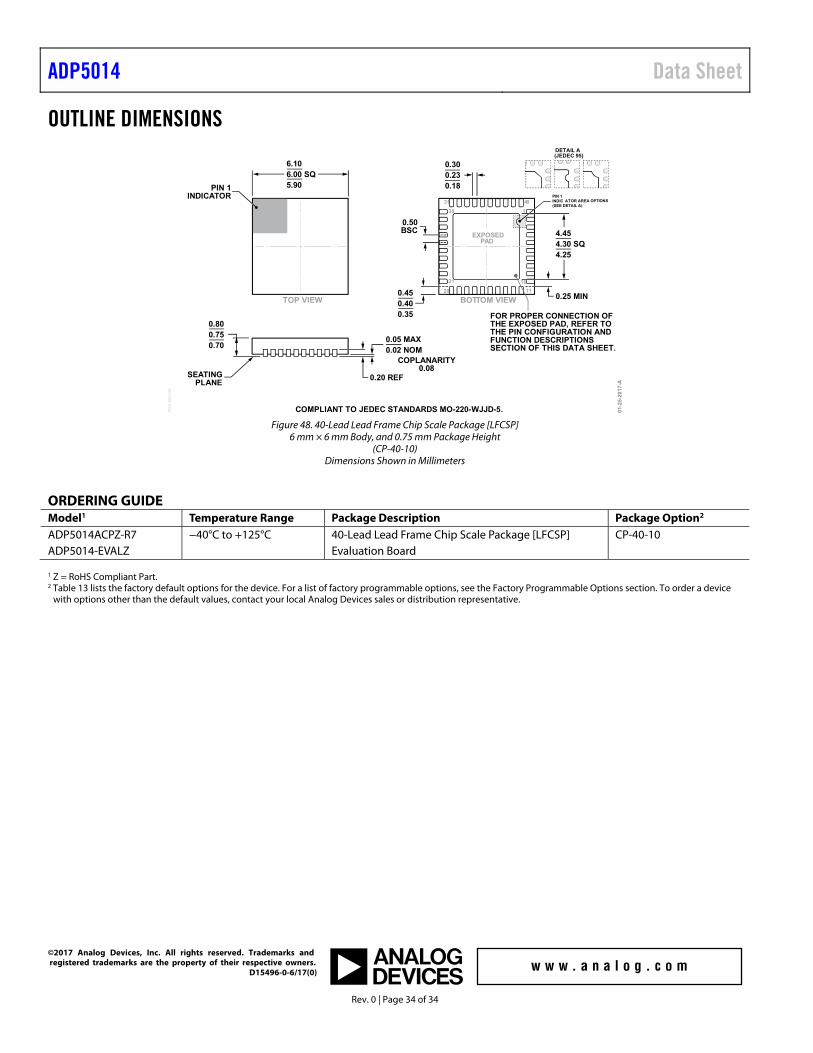
ADP5014 Data Sheet
Rev. 0 | Page 34 of 34
OUTLINE DIMENSIONS
01-
25
-20
17
-A
0.50BSC
BOTTOM VIEWTOP VIEW
PIN 1INDICATOR
EXPOSEDPAD
SEATINGPLANE
0.05 MAX0.02 NOM
0.20 REF
COPLANARITY0.08
0.300.230.18
6.106.00 SQ5.90
0.800.750.70
FOR PROPER CONNECTION OFTHE EXPOSED PAD, REFER TOTHE PIN CONFIGURATION ANDFUNCTION DESCRIPTIONSSECTION OF THIS DATA SHEET.
0.450.400.35
0.25 MIN
4.454.30 SQ4.25
COMPLIANT TO JEDEC STANDARDS MO-220-WJJD-5.
40
1
1120
21
30
31
10
PK
G-0
03
43
8
PIN 1INDIC ATOR AREA OPTIONS(SEE DETAIL A)
DETAIL A(JEDEC 95)
Figure 48. 40-Lead Lead Frame Chip Scale Package [LFCSP]
6 mm × 6 mm Body, and 0.75 mm Package Height (CP-40-10)
Dimensions Shown in Millimeters
ORDERING GUIDE Model1 Temperature Range Package Description Package Option2 ADP5014ACPZ-R7 −40°C to +125°C 40-Lead Lead Frame Chip Scale Package [LFCSP] CP-40-10 ADP5014-EVALZ Evaluation Board 1 Z = RoHS Compliant Part. 2 Table 13 lists the factory default options for the device. For a list of factory programmable options, see the Factory Programmable Options section. To order a device
with options other than the default values, contact your local Analog Devices sales or distribution representative.
©2017 Analog Devices, Inc. All rights reserved. Trademarks and registered trademarks are the property of their respective owners. D15496-0-6/17(0)