improvements of synchronous rectification on llc-dcx · voltage sensing synchronous rectification...
TRANSCRIPT
Improvements of Synchronous Rectification
on LLC-DCX
Oscar Nando Yu
Thesis submitted to the faculty of the
Virginia Polytechnic Institute and State
University in partial fulfillment of the requirements
for the degree of
Master of Science
In
Electrical Engineering
Jih-Sheng Lai, Chair
Qiang Li
Dong S. Ha
September 10, 2018
Blacksburg, Virginia
Keywords: llc dc transformer, synchronous rectification, duty cycle rate limiting,
sequential parallel switching, multilevel gate driving
Copyright © 2018 Oscar Nando Yu
Improvements of Synchronous Rectification on LLC-DCX
Oscar Nando Yu
(ABSTRACT)
LLC-based DC transformers (DCX) provide an efficient means of DC-to-DC
energy conversion due to its soft-switching capabilities. Traditionally, these LLC-DCXs
use passive diodes on the secondary side to provide a DC output. These diodes are a large
source of loss in DCXs due to the diodes’ forward drop. Synchronous rectification (SR),
provides a method of removing this diode forward drop by replacing said diode with a
diode-synchronous switch to bypass current. However, direct implementation of SR on
LLC-DCXs will experience issues such as light load resonance, and early SR switch turn-
off.
LLC-DCXs are based off of unidirectional LLC-resonant converters, which are able
to achieve very high levels of efficiency by eliminating switching losses typically incurred
during hard-switched power conversion. This is achieved through either zero voltage
switching (ZVS) or zero current switching (ZCS), through a combination of passive
components to form a resonant tank. The resulting waveform however, needs to be rectified
to obtain a DC output. In traditional topologies, passive diodes are used for rectification on
the secondary side. Passive diodes, while reliable, are a source of loss in the overall system
due to its forward drop. Circuits designed to remove this diode drop, by synchronously
turning on and off a diode-parallel switch, are coined synchronous rectifiers. Drain-source
voltage sensing synchronous rectification is a method commonly used in SR systems.
However, directly implementing this SR method on LLC-DCXs will introduce light load
resonance, and an early turn-off issue that can be detrimental to overall rectifier stability
and efficiency.
This thesis will explore two issues: current resonance and early SR turn-off. The
problems will be root-caused, solutions proposed, and the solutions verified. Finally,
current and future research work on these topics will be discussed.
Improvements of Synchronous Rectification on LLC-DCX
Oscar Nando Yu
GENERAL AUDIENCE ABSTRACT
This thesis focuses on developments and improvements on synchronous rectifiers
for resonant based power converter circuits. Traditionally, synchronous rectifiers are
implemented on high current circuits. New problems can arise when utilizing synchronous
rectification on low current circuits. This research details an internal resonance issue that
arises during implementation. The issue is root caused, simulated, and a novel solution is
presented in the form of a digital bandwidth limiter. A second issue, an early turn-off issue,
is discussed, simulated, and two new solutions are proposed depending on the rectifier
architecture. These solutions are tested, and the efficiency improvements with these
proposed methods quantified with simulations.

iv
ACKNOWLEDGEMENTS
I would like to express my deepest thanks to my advisor, Dr. Jih-Sheng Lai.
I would also like to profusely thank Chih-Shen Yeh, Xiaonan Zhao and Hsin-Che Hsieh
for motivation, critique, and allowing me bounce ideas off of them throughout the course
of this thesis.
v
Table of Contents
Chapter 1 INTRODUCTION …………………………………………...………………...1
Chapter 2 LLC-DCX AND SR INTRODUCTION …………………………………….....4
2.1 LLC-DCX INTRODUCTION…………………………………………………….…………………….....4
2.2 DRAIN-SOURCE VOLTAGE SENSING SYNCHRONOUS RECTIFICATION FOR LLC-DCX
CONVERTERS…………………………………………………………………………….………………….10
2.3 LLC-DCX MODULE SPECIFICATIONS……………………………………………………………….15
2.4 THESIS OVERVIEW AND OBJECTIVE…………………………………………………………...….16
Chapter 3 CURRENT RESONANCE ISSUE……………………………………………18
3.1 TI DRAIN-SOURCE SR RECTIFIER BOARD………………………………………………………..18
3.2 CURREMT RESONANCE ISSUE OVERVIEW……………………………………………………....22
3.3 CURRENT RESONANCE ISSUE ROOT CAUSE…………………………………………………….26
3.4 CURRENT RESONANCE SIMULATIONS…………………………………………………………...29
3.5 FPGA DUTY CYCLE RATE LIMITING………………………………………………………………34
3.6 TEST RESULTS………………………………………………………………………………………...39
Chapter 4 EARLY TURN-OFF ISSUE…………………………………………………..40
4.1 EARLY TURN-OFF ISSUE OVERVIEW………………………………………………………………40
4.2 SEQUENTIAL PARALLEL SWITCHING INTRODUCTION…………………………………………42
4.3 SEQUENTIAL PARALLEL SWITCHING SIMULATIONS AND ANALYSIS……………………….43
4.4 IMPLEMENTATION METHODS……………………………………………………………………….47
4.5 TEST RESULTS………………………………………………………………………………………….49
4.6 RECTIFIER EFFICIENCY IMPROVEMENT…………………………………………………………..52

vi
4.7 MULTILEVEL GATE DRIVER TURN-OFF…………………………………………………………...55
Chapter 5 CONCLUSION AND FUTURE WORK……………………………………...59
REFERENCES..................................................................................................................60
vii
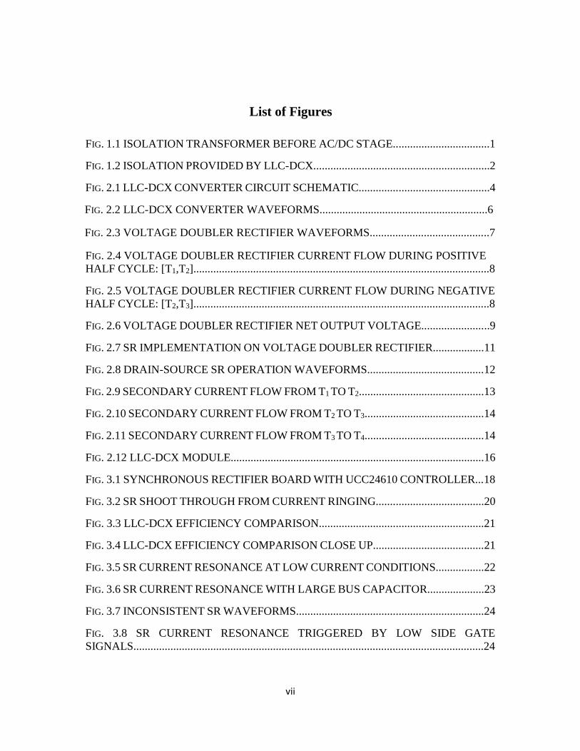
List of Figures
FIG. 1.1 ISOLATION TRANSFORMER BEFORE AC/DC STAGE..................................1
FIG. 1.2 ISOLATION PROVIDED BY LLC-DCX..............................................................2
FIG. 2.1 LLC-DCX CONVERTER CIRCUIT SCHEMATIC..............................................4
FIG. 2.2 LLC-DCX CONVERTER WAVEFORMS...........................................................6
FIG. 2.3 VOLTAGE DOUBLER RECTIFIER WAVEFORMS..........................................7
FIG. 2.4 VOLTAGE DOUBLER RECTIFIER CURRENT FLOW DURING POSITIVE
HALF CYCLE: [T1,T2]........................................................................................................8
FIG. 2.5 VOLTAGE DOUBLER RECTIFIER CURRENT FLOW DURING NEGATIVE
HALF CYCLE: [T2,T3]........................................................................................................8
FIG. 2.6 VOLTAGE DOUBLER RECTIFIER NET OUTPUT VOLTAGE........................9
FIG. 2.7 SR IMPLEMENTATION ON VOLTAGE DOUBLER RECTIFIER..................11
FIG. 2.8 DRAIN-SOURCE SR OPERATION WAVEFORMS.........................................12
FIG. 2.9 SECONDARY CURRENT FLOW FROM T1 TO T2............................................13
FIG. 2.10 SECONDARY CURRENT FLOW FROM T2 TO T3..........................................14
FIG. 2.11 SECONDARY CURRENT FLOW FROM T3 TO T4..........................................14
FIG. 2.12 LLC-DCX MODULE.........................................................................................16
FIG. 3.1 SYNCHRONOUS RECTIFIER BOARD WITH UCC24610 CONTROLLER...18
FIG. 3.2 SR SHOOT THROUGH FROM CURRENT RINGING......................................20
FIG. 3.3 LLC-DCX EFFICIENCY COMPARISON..........................................................21
FIG. 3.4 LLC-DCX EFFICIENCY COMPARISON CLOSE UP.......................................21
FIG. 3.5 SR CURRENT RESONANCE AT LOW CURRENT CONDITIONS.................22
FIG. 3.6 SR CURRENT RESONANCE WITH LARGE BUS CAPACITOR....................23
FIG. 3.7 INCONSISTENT SR WAVEFORMS..................................................................24
FIG. 3.8 SR CURRENT RESONANCE TRIGGERED BY LOW SIDE GATE
SIGNALS...........................................................................................................................24
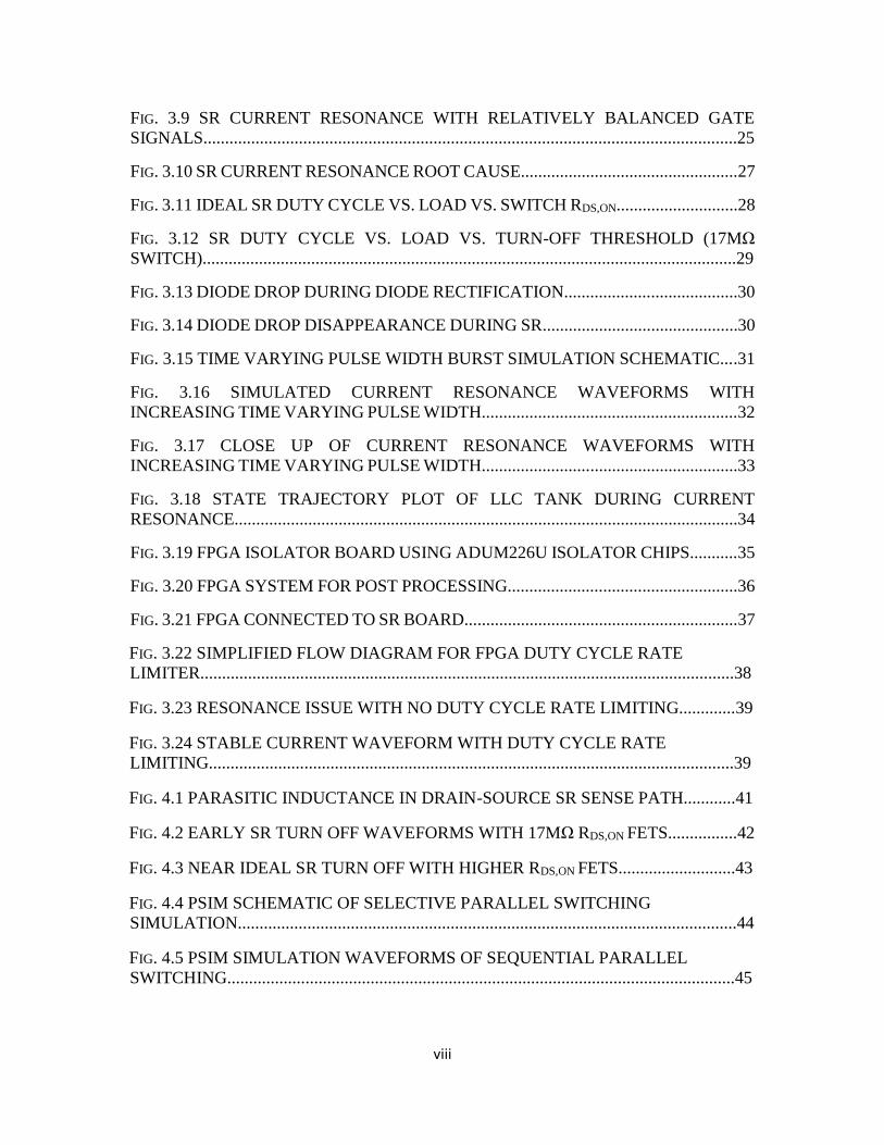
viii
FIG. 3.9 SR CURRENT RESONANCE WITH RELATIVELY BALANCED GATE
SIGNALS...........................................................................................................................25
FIG. 3.10 SR CURRENT RESONANCE ROOT CAUSE..................................................27
FIG. 3.11 IDEAL SR DUTY CYCLE VS. LOAD VS. SWITCH RDS,ON............................28
FIG. 3.12 SR DUTY CYCLE VS. LOAD VS. TURN-OFF THRESHOLD (17MΩ
SWITCH)...........................................................................................................................29
FIG. 3.13 DIODE DROP DURING DIODE RECTIFICATION........................................30
FIG. 3.14 DIODE DROP DISAPPEARANCE DURING SR.............................................30
FIG. 3.15 TIME VARYING PULSE WIDTH BURST SIMULATION SCHEMATIC....31
FIG. 3.16 SIMULATED CURRENT RESONANCE WAVEFORMS WITH
INCREASING TIME VARYING PULSE WIDTH...........................................................32
FIG. 3.17 CLOSE UP OF CURRENT RESONANCE WAVEFORMS WITH
INCREASING TIME VARYING PULSE WIDTH...........................................................33
FIG. 3.18 STATE TRAJECTORY PLOT OF LLC TANK DURING CURRENT
RESONANCE....................................................................................................................34
FIG. 3.19 FPGA ISOLATOR BOARD USING ADUM226U ISOLATOR CHIPS...........35
FIG. 3.20 FPGA SYSTEM FOR POST PROCESSING.....................................................36
FIG. 3.21 FPGA CONNECTED TO SR BOARD...............................................................37
FIG. 3.22 SIMPLIFIED FLOW DIAGRAM FOR FPGA DUTY CYCLE RATE
LIMITER...........................................................................................................................38
FIG. 3.23 RESONANCE ISSUE WITH NO DUTY CYCLE RATE LIMITING.............39
FIG. 3.24 STABLE CURRENT WAVEFORM WITH DUTY CYCLE RATE
LIMITING.........................................................................................................................39
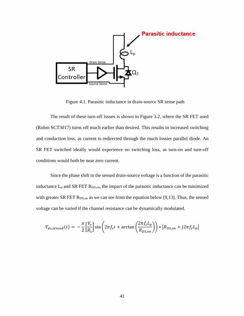
FIG. 4.1 PARASITIC INDUCTANCE IN DRAIN-SOURCE SR SENSE PATH............41
FIG. 4.2 EARLY SR TURN OFF WAVEFORMS WITH 17MΩ RDS,ON FETS................42
FIG. 4.3 NEAR IDEAL SR TURN OFF WITH HIGHER RDS,ON FETS...........................43
FIG. 4.4 PSIM SCHEMATIC OF SELECTIVE PARALLEL SWITCHING
SIMULATION...................................................................................................................44
FIG. 4.5 PSIM SIMULATION WAVEFORMS OF SEQUENTIAL PARALLEL
SWITCHING.....................................................................................................................45
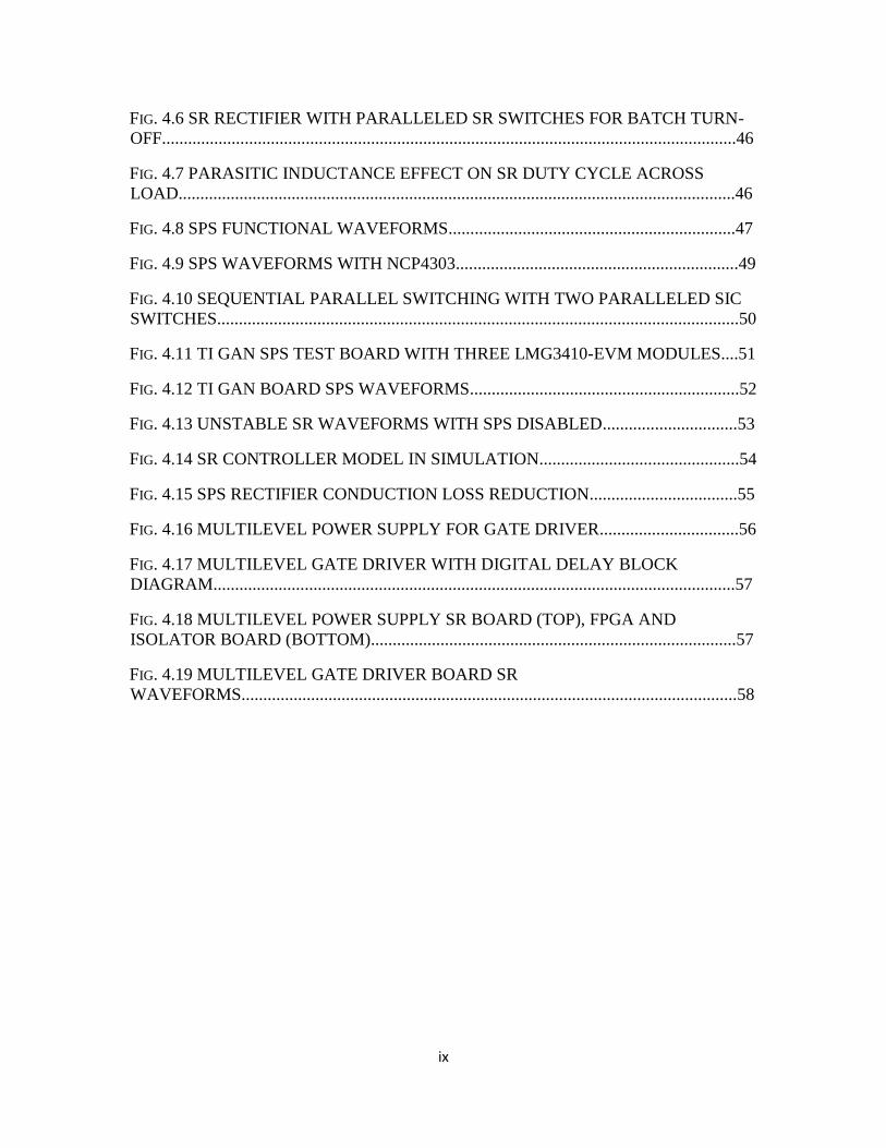
ix
FIG. 4.6 SR RECTIFIER WITH PARALLELED SR SWITCHES FOR BATCH TURN-
OFF....................................................................................................................................46
FIG. 4.7 PARASITIC INDUCTANCE EFFECT ON SR DUTY CYCLE ACROSS
LOAD................................................................................................................................46
FIG. 4.8 SPS FUNCTIONAL WAVEFORMS..................................................................47
FIG. 4.9 SPS WAVEFORMS WITH NCP4303.................................................................49
FIG. 4.10 SEQUENTIAL PARALLEL SWITCHING WITH TWO PARALLELED SIC
SWITCHES........................................................................................................................50
FIG. 4.11 TI GAN SPS TEST BOARD WITH THREE LMG3410-EVM MODULES....51
FIG. 4.12 TI GAN BOARD SPS WAVEFORMS..............................................................52
FIG. 4.13 UNSTABLE SR WAVEFORMS WITH SPS DISABLED...............................53
FIG. 4.14 SR CONTROLLER MODEL IN SIMULATION..............................................54
FIG. 4.15 SPS RECTIFIER CONDUCTION LOSS REDUCTION..................................55
FIG. 4.16 MULTILEVEL POWER SUPPLY FOR GATE DRIVER................................56
FIG. 4.17 MULTILEVEL GATE DRIVER WITH DIGITAL DELAY BLOCK
DIAGRAM........................................................................................................................57
FIG. 4.18 MULTILEVEL POWER SUPPLY SR BOARD (TOP), FPGA AND
ISOLATOR BOARD (BOTTOM)....................................................................................57
FIG. 4.19 MULTILEVEL GATE DRIVER BOARD SR
WAVEFORMS..................................................................................................................58
x
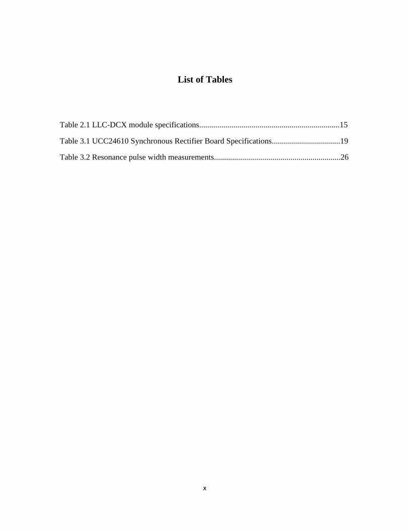
List of Tables
Table 2.1 LLC-DCX module specifications......................................................................15
Table 3.1 UCC24610 Synchronous Rectifier Board Specifications..................................19
Table 3.2 Resonance pulse width measurements...............................................................26
1
CHAPTER 1: INTRODUCTION
High voltage power electronics are in an ever increasing demand for utility,
datacenter and other high power applications. One possible use for high voltage power
electronics is in solid-state transformers (SST). Solid-state transformers are built with
multiple solid state power converters, and serve to replace traditional transformers. Solid-
state transformers feature voltage regulation, constant unity power factor, overload
protection, and many other benefits traditional wire wound transformers are unable to
provide [2].
Due to the high voltages present in the system, isolation becomes a large concern
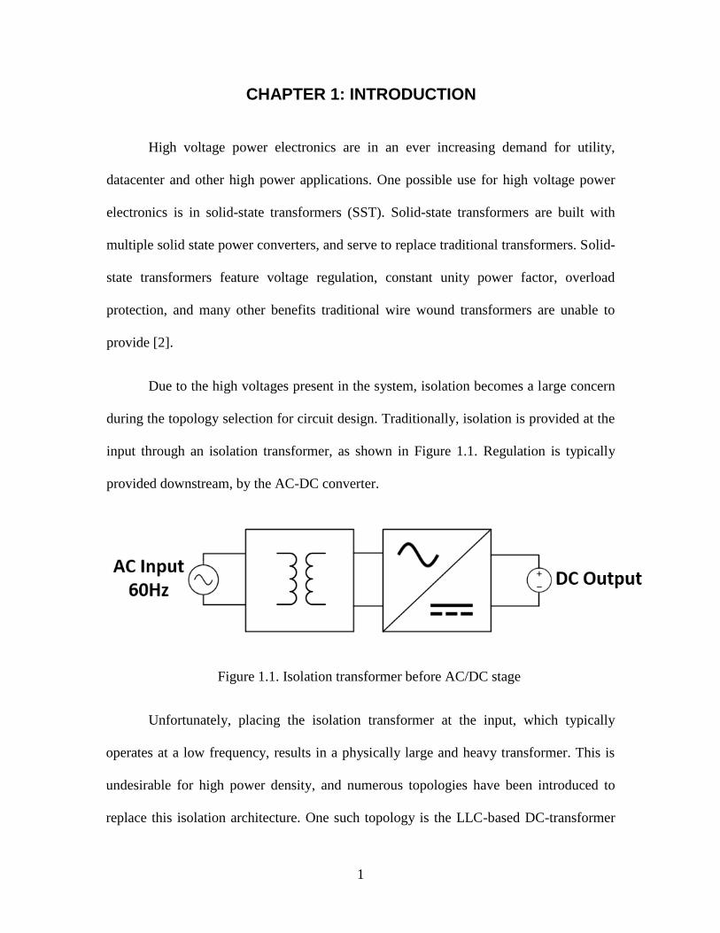
during the topology selection for circuit design. Traditionally, isolation is provided at the
input through an isolation transformer, as shown in Figure 1.1. Regulation is typically
provided downstream, by the AC-DC converter.
Figure 1.1. Isolation transformer before AC/DC stage
Unfortunately, placing the isolation transformer at the input, which typically
operates at a low frequency, results in a physically large and heavy transformer. This is
undesirable for high power density, and numerous topologies have been introduced to
replace this isolation architecture. One such topology is the LLC-based DC-transformer
2
circuit. The LLC DC-transformer, henceforth called the LLC-DCX, is an isolated, soft
switched DC-DC converter optimized around a single conversion ratio. Isolation is
provided by a transformer in the circuit. Since the switching frequency, and thus excitation
frequency of the transformer can be controlled, the physical size of the transformer can be
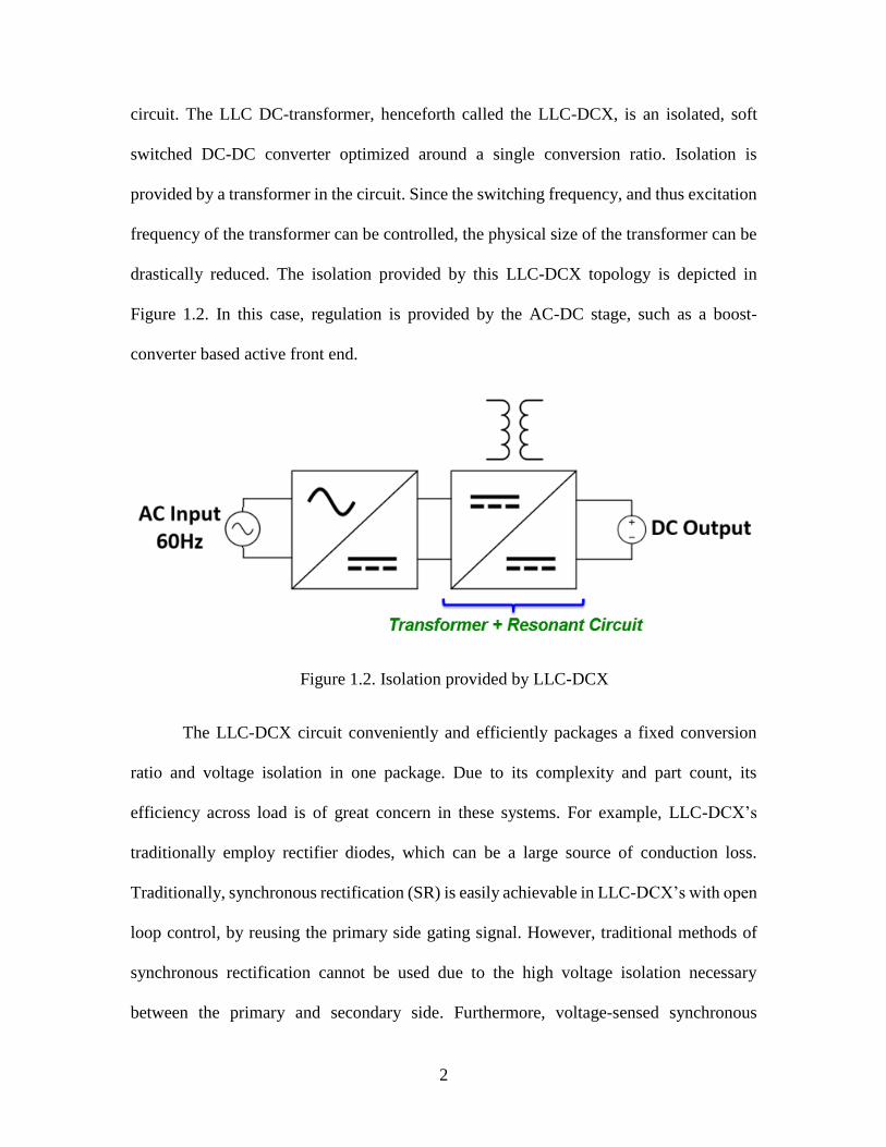
drastically reduced. The isolation provided by this LLC-DCX topology is depicted in
Figure 1.2. In this case, regulation is provided by the AC-DC stage, such as a boost-
converter based active front end.
Figure 1.2. Isolation provided by LLC-DCX
The LLC-DCX circuit conveniently and efficiently packages a fixed conversion
ratio and voltage isolation in one package. Due to its complexity and part count, its
efficiency across load is of great concern in these systems. For example, LLC-DCX’s
traditionally employ rectifier diodes, which can be a large source of conduction loss.
Traditionally, synchronous rectification (SR) is easily achievable in LLC-DCX’s with open
loop control, by reusing the primary side gating signal. However, traditional methods of
synchronous rectification cannot be used due to the high voltage isolation necessary
between the primary and secondary side. Furthermore, voltage-sensed synchronous
3
rectification, a common type of SR, can suffer from an early turn-off issue that
progressively deteriorates the synchronous rectifier’s efficiency at lighter loads. It can also
suffer from a stability issue when low channel resistance power MOSFETs are used
without duty cycle rate limiting at light loads. This thesis intends to root cause and review
these issues and propose more practical, novel solutions that can be implemented in LLC-
based DC transformer circuits.
Currently, only the early turn-off issue has been identified in previous research [14-
15]. Two related solutions were proposed: 1) a zero crossing filter and 2) an auxiliary SR
compensation circuit. Both circuits base their working principle on developing a drain-
source signal for the SR FET controller that is not affected by the parasitics present in the
circuit. These methods rely on an auxiliary circuit that is tuned exactly to the parasitic
inductance in the SR rectifier current path and RDS,on of the SR switch. As a result, tuning
the circuit can be troublesome, time consuming, and inaccurate under condition change
(such as temperature). The novel methods proposed, sequential parallel switching and
multilevel gate driving, do not rely on tuning the compensating circuit to the parasitics.
Thus, the methods proposed in this thesis for alleviating the early turn-off issue are much
more practical to implement in real world systems.
4
CHAPTER 2: LLC-DCX AND SR INTRODUCTION
2.1 LLC-DCX Introduction
The LLC-DCX (DC transformer) is a resonant-based DC to DC converter popularly
used due to its ease of implementation and efficiency. Due to its soft switching capabilities,
its power conversion efficiency can far exceed traditional hard-switched converters. This
makes it very attractive for high power applications such as solid-state transformers [1-2].
The heart of the LLC converter lies in the resonant tank, a passive tank consisting
of three reactive components: two inductors and a capacitor. This resonant tank has two
frequencies associated with it – one higher, and one lower. The higher frequency is
generally referred to as the resonant frequency of the tank, fo. A half bridge LLC converter
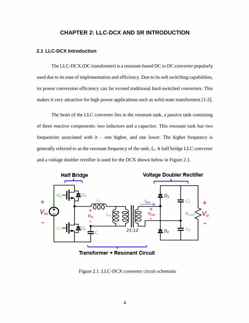
and a voltage doubler rectifier is used for the DCX shown below in Figure 2.1.
Figure 2.1. LLC-DCX converter circuit schematic
5
Lr and Cr, the resonant inductor and resonant capacitor respectively, represent the
higher main resonant frequency. This frequency can be calculated by:
𝑓𝑟 =1
2𝜋√𝐿𝑟𝐶𝑟
This only represents one of the two resonant tank frequencies, however. If the
transformer secondaries in the circuit are left open, the tank turns into a two element tank,
summing Lm, the magnetizing inductance, and Lr. This results in the second resonant tank
frequency:
𝑓𝑟2 =1
2𝜋√(𝐿𝑟 + 𝐿𝑚)𝐶𝑟
This second resonant frequency is much lower than the primary resonant frequency,
and is typically not used often during the design process. The main resonant tank is excited
at a certain frequency, which then determines the amount of power flow from input to
output. For maximum efficiency the converter must be operated around the normalized
frequency of 1, the higher resonant tank frequency of the LLC converter. This is the
frequency the LLC-DCX is excited at, in order to operate at maximum efficiency. This
operating point allows for zero voltage switching (ZVS) with the primary switches with
properly designed Lm values, and zero current switching (ZCS) on the secondary with ideal
synchronous rectification. Lm, the magnetizing inductor of the transformer, and Lr are
typically designed a part of the transformer, representing the leakage and magnetizing
inductance respectively. The magnetizing inductance is sized appropriately to discharge
the primary MOSFET’s junction capacitors, resulting in soft switching. The MOSFET’s
6
junction capacitance, switching frequency, and switch dead time must all be taken into
account for proper design of Lm [3].
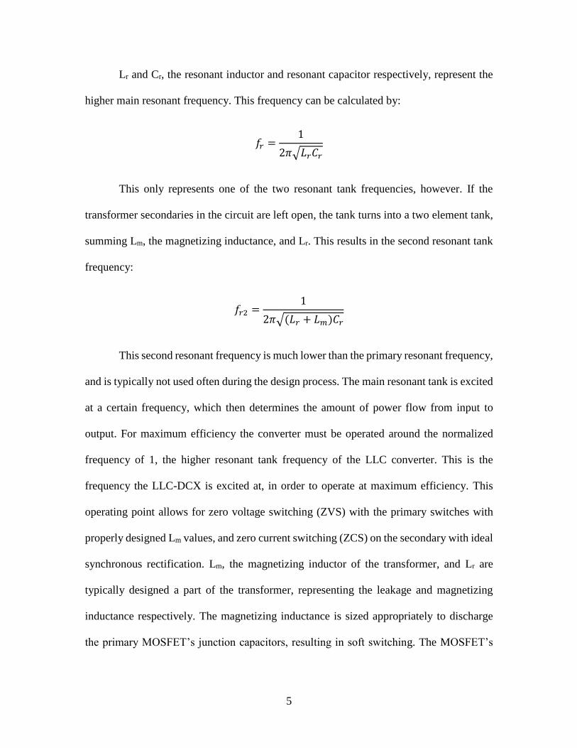
Figure 2.2. LLC-DCX converter waveforms
In an LLC-DCX, the converter is run in open loop with fixed switch dead time and
50% duty cycle. The switching and resulting waveforms can be seen in Figure 2.2, which
results in a secondary square voltage wave, and a pseudo-sinusoidal current waveform. To
achieve a DC output, the waveform must be rectified. A voltage doubler rectifier is used
as shown in Figure 2.1. Voltage-doubler-specific waveforms are shown in Figure 2.3.
7
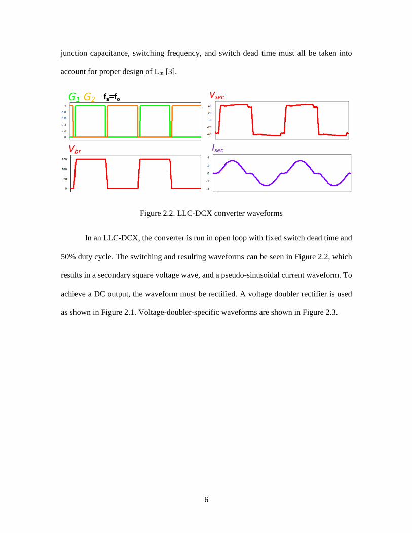
Figure 2.3. Voltage doubler rectifier waveforms
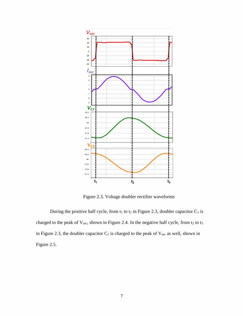
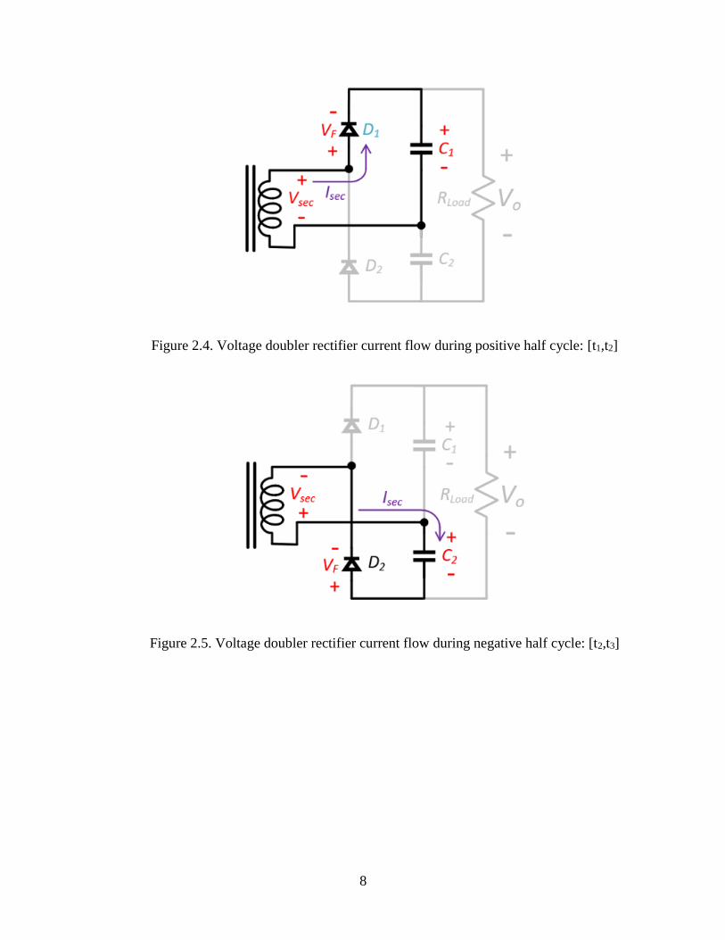
During the positive half cycle, from t1 to t2 in Figure 2.3, doubler capacitor C1 is
charged to the peak of Vsec, shown in Figure 2.4. In the negative half cycle, from t2 to t3
in Figure 2.3, the doubler capacitor C2 is charged to the peak of Vsec as well, shown in
Figure 2.5.
8
Figure 2.4. Voltage doubler rectifier current flow during positive half cycle: [t1,t2]
Figure 2.5. Voltage doubler rectifier current flow during negative half cycle: [t2,t3]
9
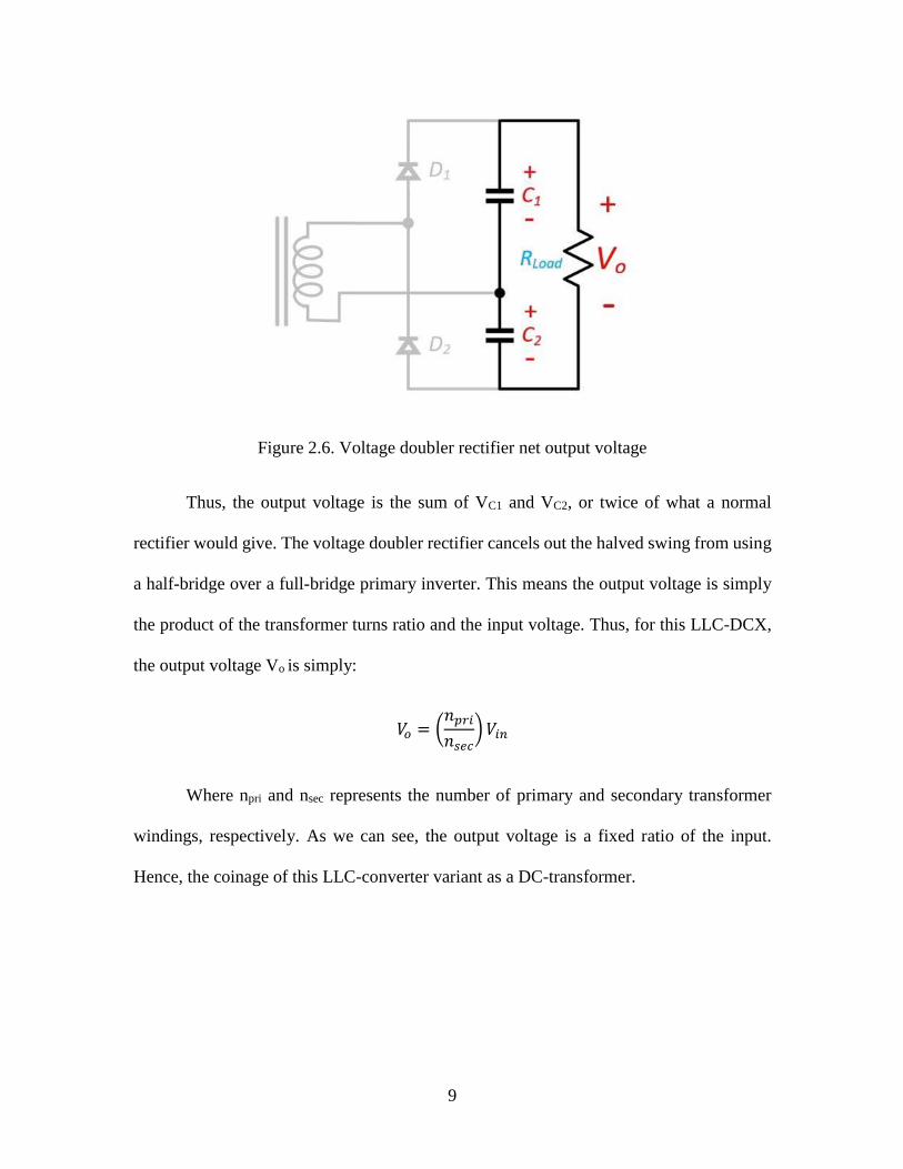
Figure 2.6. Voltage doubler rectifier net output voltage
Thus, the output voltage is the sum of VC1 and VC2, or twice of what a normal
rectifier would give. The voltage doubler rectifier cancels out the halved swing from using
a half-bridge over a full-bridge primary inverter. This means the output voltage is simply
the product of the transformer turns ratio and the input voltage. Thus, for this LLC-DCX,
the output voltage Vo is simply:
𝑉𝑜 = (𝑛𝑝𝑟𝑖
𝑛𝑠𝑒𝑐) 𝑉𝑖𝑛
Where npri and nsec represents the number of primary and secondary transformer
windings, respectively. As we can see, the output voltage is a fixed ratio of the input.
Hence, the coinage of this LLC-converter variant as a DC-transformer.
10
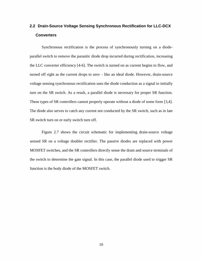
2.2 Drain-Source Voltage Sensing Synchronous Rectification for LLC-DCX
Converters
Synchronous rectification is the process of synchronously turning on a diode-
parallel switch to remove the parasitic diode drop incurred during rectification, increasing
the LLC converter efficiency [4-6]. The switch is turned on as current begins to flow, and
turned off right as the current drops to zero – like an ideal diode. However, drain-source
voltage sensing synchronous rectification uses the diode conduction as a signal to initially
turn on the SR switch. As a result, a parallel diode is necessary for proper SR function.
These types of SR controllers cannot properly operate without a diode of some form [3,4].
The diode also serves to catch any current not conducted by the SR switch, such as in late
SR switch turn on or early switch turn off.
Figure 2.7 shows the circuit schematic for implementing drain-source voltage
sensed SR on a voltage doubler rectifier. The passive diodes are replaced with power
MOSFET switches, and the SR controllers directly sense the drain and source terminals of
the switch to determine the gate signal. In this case, the parallel diode used to trigger SR
function is the body diode of the MOSFET switch.
11
Figure 2.7. SR implementation on voltage doubler rectifier
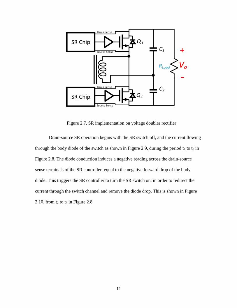
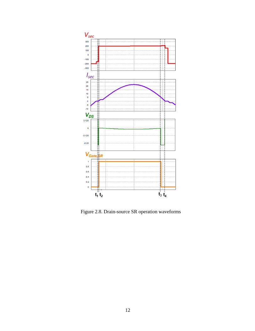
Drain-source SR operation begins with the SR switch off, and the current flowing
through the body diode of the switch as shown in Figure 2.9, during the period t1 to t2 in
Figure 2.8. The diode conduction induces a negative reading across the drain-source
sense terminals of the SR controller, equal to the negative forward drop of the body
diode. This triggers the SR controller to turn the SR switch on, in order to redirect the
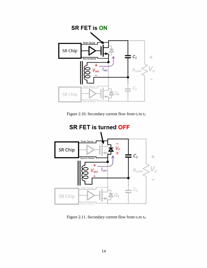
current through the switch channel and remove the diode drop. This is shown in Figure
2.10, from t2 to t3 in Figure 2.8.
12
Figure 2.8. Drain-source SR operation waveforms
13
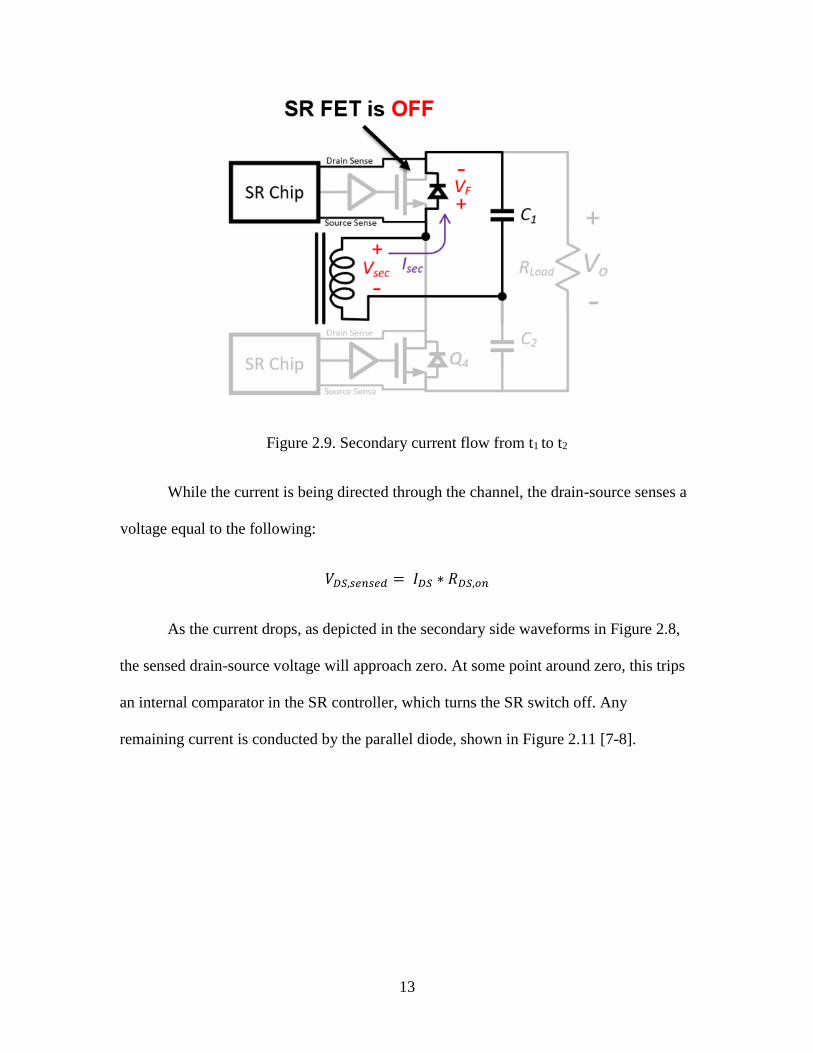
Figure 2.9. Secondary current flow from t1 to t2
While the current is being directed through the channel, the drain-source senses a
voltage equal to the following:
𝑉𝐷𝑆,𝑠𝑒𝑛𝑠𝑒𝑑 = 𝐼𝐷𝑆 ∗ 𝑅𝐷𝑆,𝑜𝑛
As the current drops, as depicted in the secondary side waveforms in Figure 2.8,
the sensed drain-source voltage will approach zero. At some point around zero, this trips
an internal comparator in the SR controller, which turns the SR switch off. Any
remaining current is conducted by the parallel diode, shown in Figure 2.11 [7-8].
14
Figure 2.10. Secondary current flow from t2 to t3
Figure 2.11. Secondary current flow from t3 to t4
15
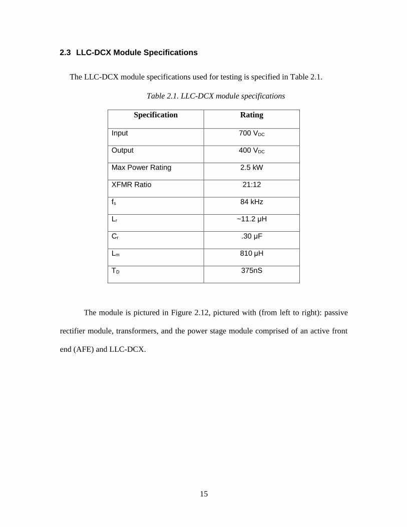
2.3 LLC-DCX Module Specifications
The LLC-DCX module specifications used for testing is specified in Table 2.1.
Table 2.1. LLC-DCX module specifications
Specification Rating
Input 700 VDC
Output 400 VDC
Max Power Rating 2.5 kW
XFMR Ratio 21:12
fs 84 kHz
Lr ~11.2 μH
Cr .30 μF
Lm 810 μH
TD 375nS
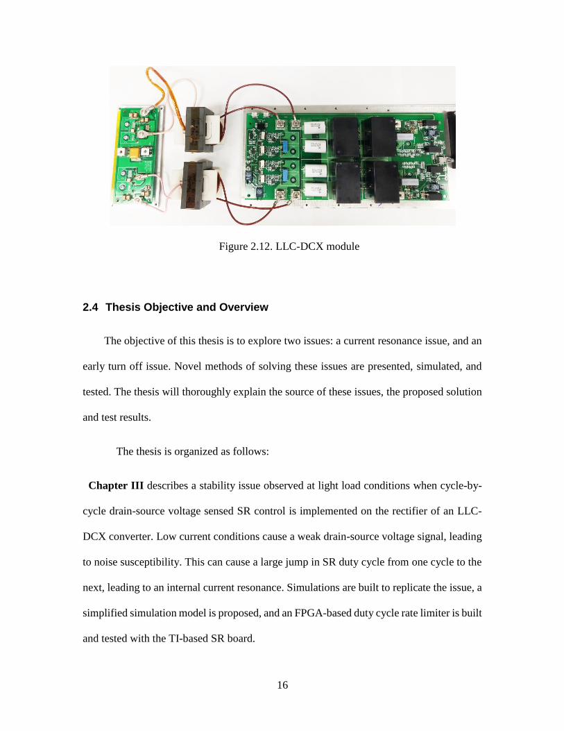
The module is pictured in Figure 2.12, pictured with (from left to right): passive
rectifier module, transformers, and the power stage module comprised of an active front
end (AFE) and LLC-DCX.
16
Figure 2.12. LLC-DCX module
2.4 Thesis Objective and Overview
The objective of this thesis is to explore two issues: a current resonance issue, and an
early turn off issue. Novel methods of solving these issues are presented, simulated, and
tested. The thesis will thoroughly explain the source of these issues, the proposed solution
and test results.
The thesis is organized as follows:
Chapter III describes a stability issue observed at light load conditions when cycle-by-
cycle drain-source voltage sensed SR control is implemented on the rectifier of an LLC-
DCX converter. Low current conditions cause a weak drain-source voltage signal, leading
to noise susceptibility. This can cause a large jump in SR duty cycle from one cycle to the
next, leading to an internal current resonance. Simulations are built to replicate the issue, a
simplified simulation model is proposed, and an FPGA-based duty cycle rate limiter is built
and tested with the TI-based SR board.
17
Chapter IV describes an early SR turn-off issue that occurs due to parasitics present in
the SR drain-source voltage sensing loop. Two solutions are proposed, sequential parallel
switching (SPS) for rectifiers with paralleled SR switches, and multilevel turn-off gate
driving for single SR switch rectifiers. By increasing the SR switch RDS,on near SR turn-
off, the sensed drain-source voltage can be increased, minimizing the effects of the
parasitics. This leads to longer SR conduction times, and a more efficient rectifier.
Calculations are made to compare the effects of parasitic inductance across switch RDS,on.
Simulations are run to plot rectifier efficiency gains when utilizing sequential parallel
switching.
Chapter V describes future work-in-progress for the multilevel gate driver, and
summarizes the contributions within the course of this thesis.
18
CHAPTER 3: CURRENT RESONANCE ISSUE
3.1 TI Drain-Source SR Rectifier Board
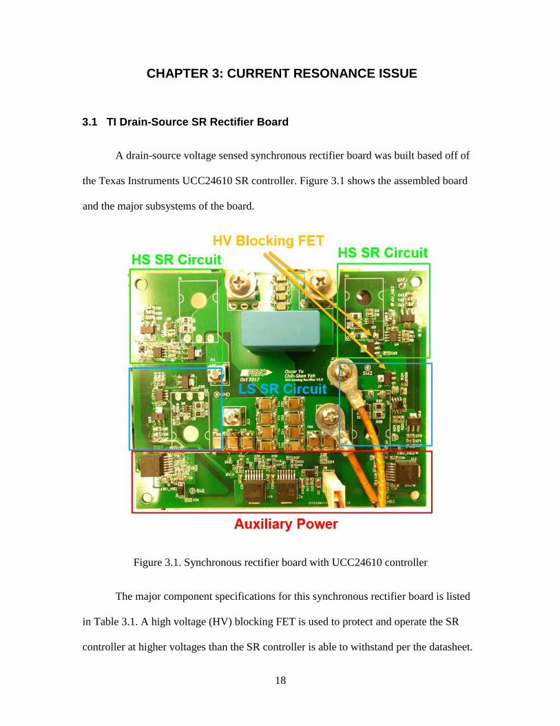
A drain-source voltage sensed synchronous rectifier board was built based off of
the Texas Instruments UCC24610 SR controller. Figure 3.1 shows the assembled board
and the major subsystems of the board.
Figure 3.1. Synchronous rectifier board with UCC24610 controller
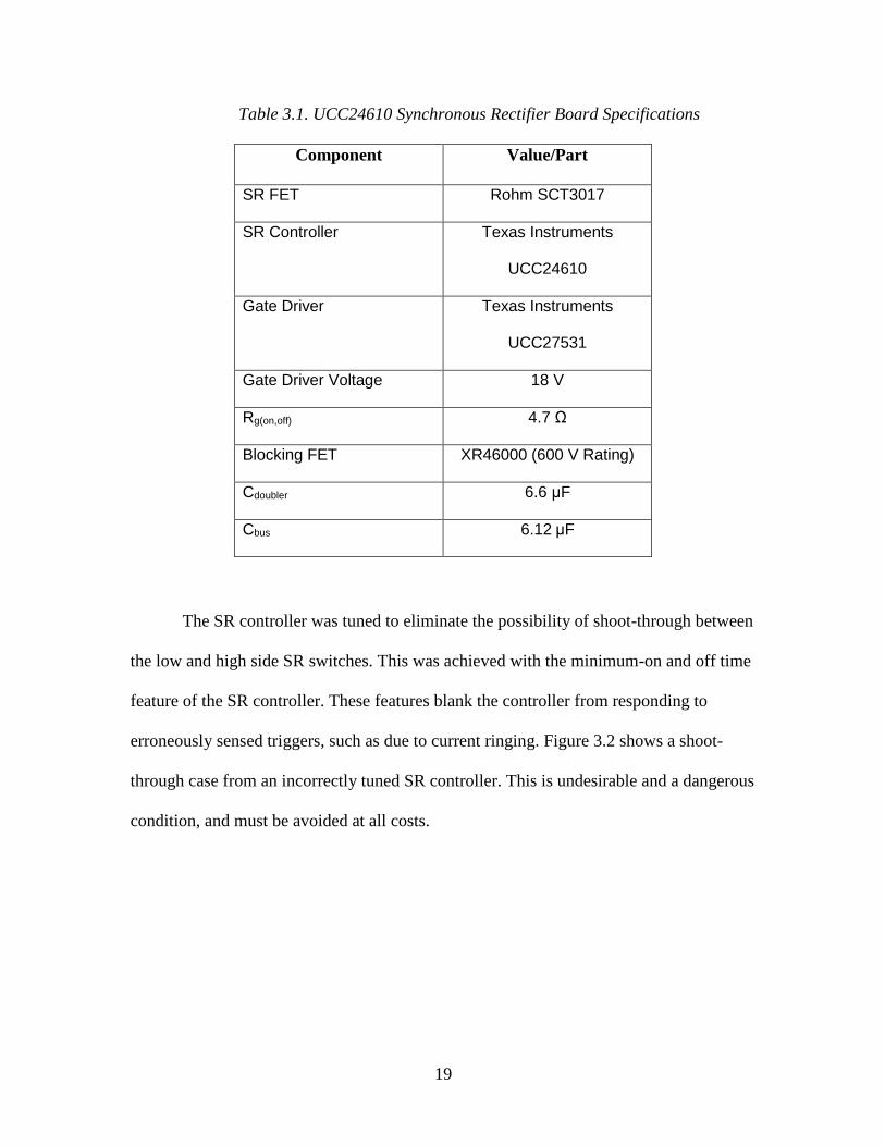
The major component specifications for this synchronous rectifier board is listed
in Table 3.1. A high voltage (HV) blocking FET is used to protect and operate the SR
controller at higher voltages than the SR controller is able to withstand per the datasheet.
19
Table 3.1. UCC24610 Synchronous Rectifier Board Specifications
Component Value/Part
SR FET Rohm SCT3017
SR Controller Texas Instruments
UCC24610
Gate Driver Texas Instruments
UCC27531
Gate Driver Voltage 18 V
Rg(on,off) 4.7 Ω
Blocking FET XR46000 (600 V Rating)
Cdoubler 6.6 μF
Cbus 6.12 μF
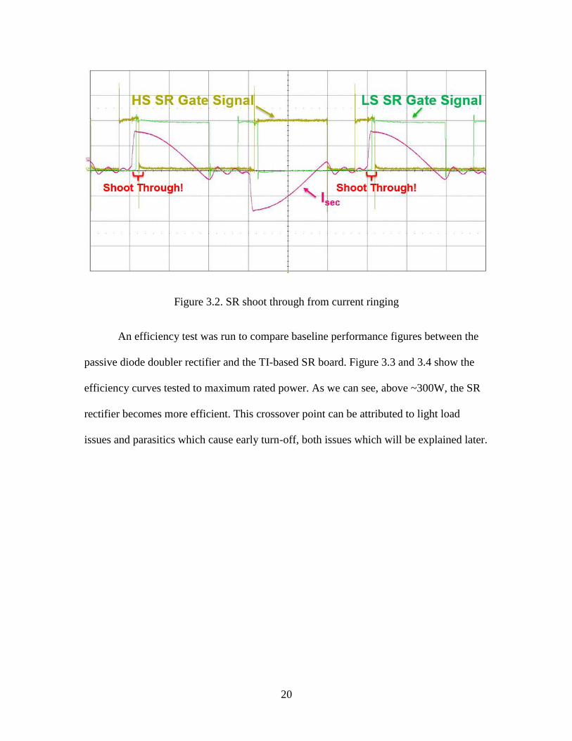
The SR controller was tuned to eliminate the possibility of shoot-through between
the low and high side SR switches. This was achieved with the minimum-on and off time
feature of the SR controller. These features blank the controller from responding to
erroneously sensed triggers, such as due to current ringing. Figure 3.2 shows a shoot-
through case from an incorrectly tuned SR controller. This is undesirable and a dangerous
condition, and must be avoided at all costs.
20
Figure 3.2. SR shoot through from current ringing
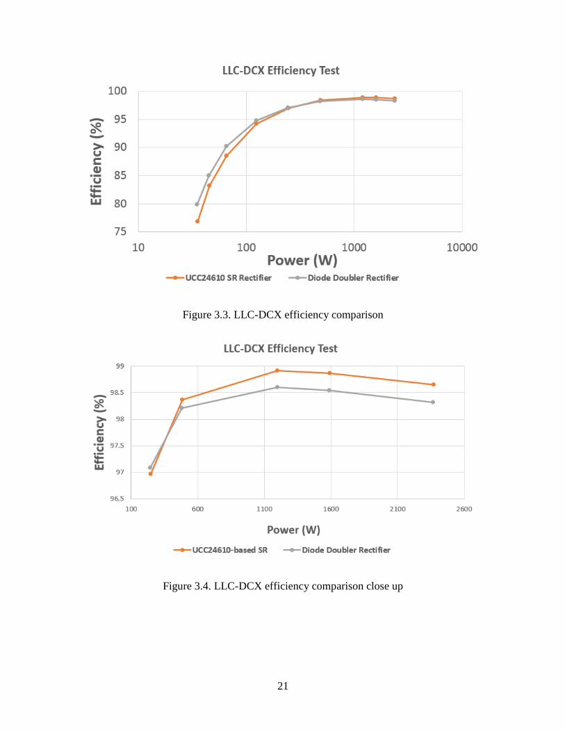
An efficiency test was run to compare baseline performance figures between the
passive diode doubler rectifier and the TI-based SR board. Figure 3.3 and 3.4 show the
efficiency curves tested to maximum rated power. As we can see, above ~300W, the SR
rectifier becomes more efficient. This crossover point can be attributed to light load
issues and parasitics which cause early turn-off, both issues which will be explained later.
21
Figure 3.3. LLC-DCX efficiency comparison
Figure 3.4. LLC-DCX efficiency comparison close up
22
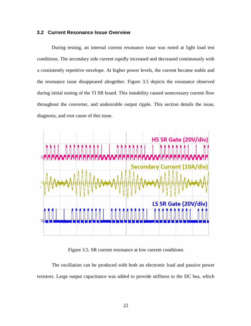
3.2 Current Resonance Issue Overview
During testing, an internal current resonance issue was noted at light load test
conditions. The secondary side current rapidly increased and decreased continuously with
a consistently repetitive envelope. At higher power levels, the current became stable and
the resonance issue disappeared altogether. Figure 3.5 depicts the resonance observed
during initial testing of the TI SR board. This instability caused unnecessary current flow
throughout the converter, and undesirable output ripple. This section details the issue,
diagnosis, and root cause of this issue.
Figure 3.5. SR current resonance at low current conditions
The oscillation can be produced with both an electronic load and passive power
resistors. Large output capacitance was added to provide stiffness to the DC bus, which
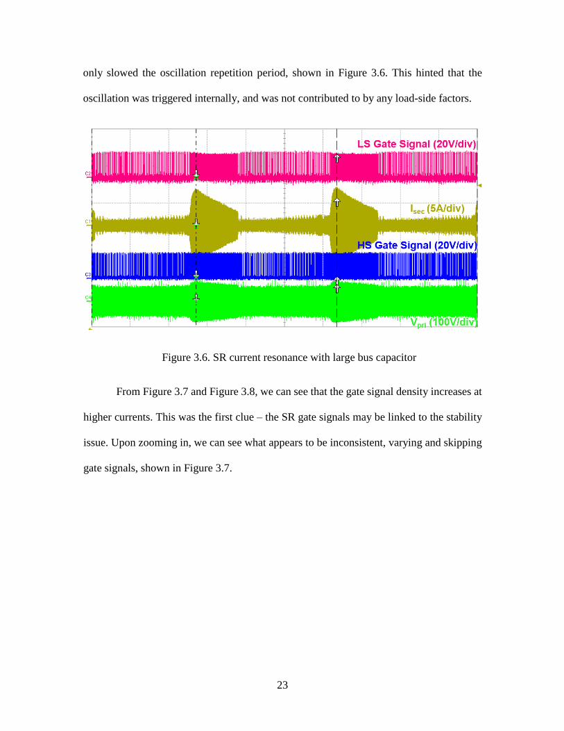
23
only slowed the oscillation repetition period, shown in Figure 3.6. This hinted that the
oscillation was triggered internally, and was not contributed to by any load-side factors.
Figure 3.6. SR current resonance with large bus capacitor
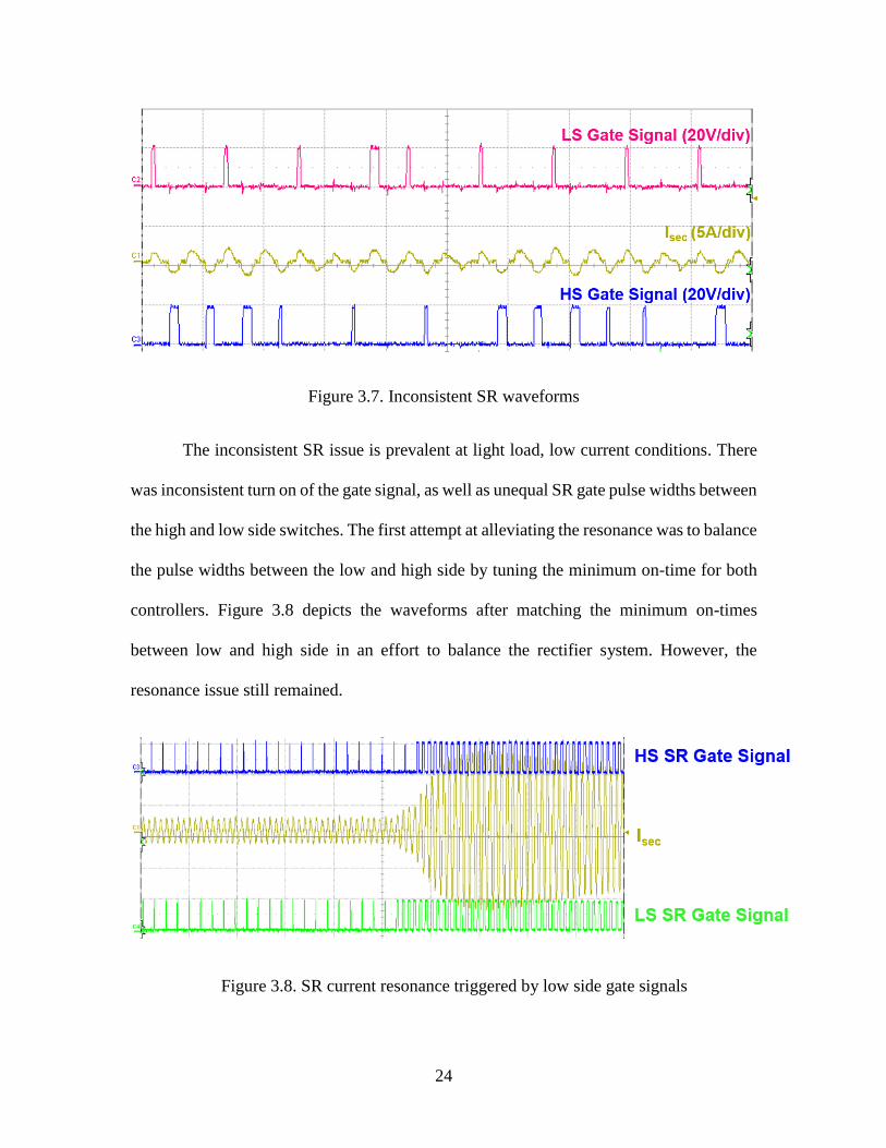
From Figure 3.7 and Figure 3.8, we can see that the gate signal density increases at
higher currents. This was the first clue – the SR gate signals may be linked to the stability
issue. Upon zooming in, we can see what appears to be inconsistent, varying and skipping
gate signals, shown in Figure 3.7.
24
Figure 3.7. Inconsistent SR waveforms
The inconsistent SR issue is prevalent at light load, low current conditions. There
was inconsistent turn on of the gate signal, as well as unequal SR gate pulse widths between
the high and low side switches. The first attempt at alleviating the resonance was to balance
the pulse widths between the low and high side by tuning the minimum on-time for both
controllers. Figure 3.8 depicts the waveforms after matching the minimum on-times
between low and high side in an effort to balance the rectifier system. However, the
resonance issue still remained.
Figure 3.8. SR current resonance triggered by low side gate signals
25
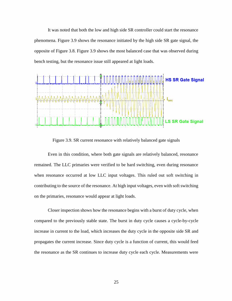
It was noted that both the low and high side SR controller could start the resonance
phenomena. Figure 3.9 shows the resonance initiated by the high side SR gate signal, the
opposite of Figure 3.8. Figure 3.9 shows the most balanced case that was observed during
bench testing, but the resonance issue still appeared at light loads.
Figure 3.9. SR current resonance with relatively balanced gate signals
Even in this condition, where both gate signals are relatively balanced, resonance
remained. The LLC primaries were verified to be hard switching, even during resonance
when resonance occurred at low LLC input voltages. This ruled out soft switching in
contributing to the source of the resonance. At high input voltages, even with soft switching
on the primaries, resonance would appear at light loads.
Closer inspection shows how the resonance begins with a burst of duty cycle, when
compared to the previously stable state. The burst in duty cycle causes a cycle-by-cycle
increase in current to the load, which increases the duty cycle in the opposite side SR and
propagates the current increase. Since duty cycle is a function of current, this would feed
the resonance as the SR continues to increase duty cycle each cycle. Measurements were
26
performed on the duty cycle of the high and low side switches during one of the resonance
conditions, shown in Table 3.2.
Table 3.2. Resonance pulse width measurements
Resonance Timeframe Low Side Pulse Width (uS) High Side Pulse Width (uS)
Pre-resonance (initial, steady state)
3.309 3.260
Middle (current rising) 3.995 4.150
Peak 4.205 4.350
Middle (current falling) 3.795 3.830
As shown, the pulse width steadily increases during the rapid current increase. This
is expected, as the SR chip’s duty cycle is a function of the SR FET drain current and RDS,on.
This hints that even an erroneous burst of duty cycle due to noise in the drain-source voltage
sensing circuit could trigger a cycle-by-cycle increase in current, causing the phenomena
shown.
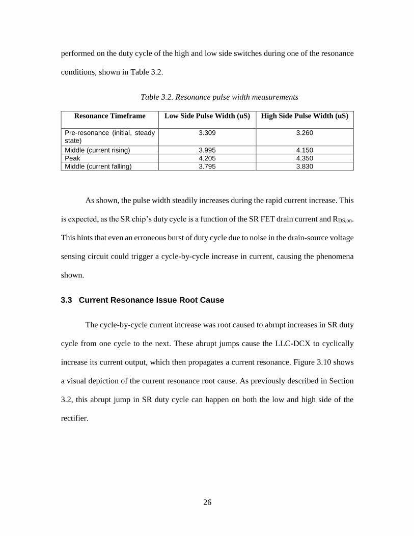
3.3 Current Resonance Issue Root Cause
The cycle-by-cycle current increase was root caused to abrupt increases in SR duty
cycle from one cycle to the next. These abrupt jumps cause the LLC-DCX to cyclically
increase its current output, which then propagates a current resonance. Figure 3.10 shows
a visual depiction of the current resonance root cause. As previously described in Section
3.2, this abrupt jump in SR duty cycle can happen on both the low and high side of the
rectifier.
27
Figure 3.10. SR current resonance root cause
The reason for the abrupt increases in SR duty cycle was traced down to a weak
drain-source voltage signal, which is especially susceptible to noise. Light load conditions
result in very low secondary side current, which the drain-source voltage sensing SR
controller attempts to measure through a shunt resistor, the SR switch’s channel resistance.
Unfortunately, with low RDS,on SR switches, the drain-source voltage magnitude near turn-
off is reduced since the magnitude is the product of the drain-source current and channel
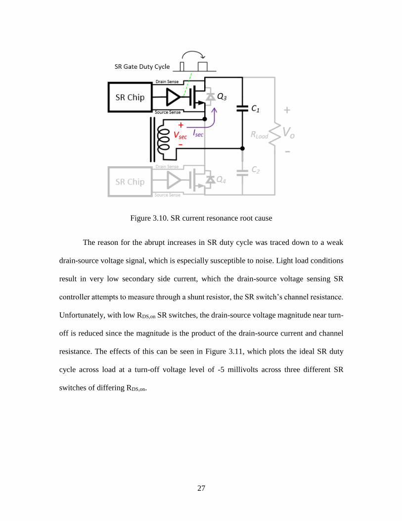
resistance. The effects of this can be seen in Figure 3.11, which plots the ideal SR duty
cycle across load at a turn-off voltage level of -5 millivolts across three different SR
switches of differing RDS,on.
28
Figure 3.11. Ideal SR duty cycle vs. Load vs. Switch RDS,on
The drain-source voltage of the SR FET can be expressed in the time domain as
sinusoid, valid for half of the switching period as shown below [9,13].
𝑉𝑑𝑠(𝑡) = −𝜋
2[
𝑉𝑜
𝑅𝐿] sin (2𝜋𝑓𝑠𝑡 + arctan (
2𝜋𝑓𝑠𝐿𝑝
𝑅𝐷𝑆,𝑜𝑛)) ∗ |𝑅𝐷𝑆,𝑜𝑛 + 𝑗2𝜋𝑓𝑠𝐿𝑝|
The SR duty cycle would just be the amount of time it takes for equation VDS(t) to
equal the turn-off threshold voltage, divided by the switching period. Ideally, the SR would
conduct at nearly 50%, the entire half cycle, across all load levels. If this were the case, the
current resonance issue would not appear as there would be no duty cycle fluctuations.
However as we can see, higher RDS,on SR switches have the advantage of longer conduction
times across load than the lower RDS,on switches do. More importantly however, higher
RDS,on switches have less susceptibility to noise since they have less of a change in duty
cycle over change in power at light load. This can be seen in Figure 3.12, when the turn-
off threshold is perturbed by +/- 2 millivolts.
29
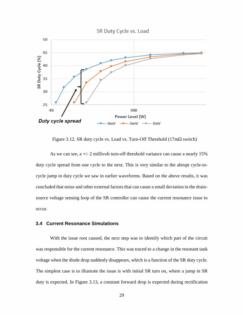
Figure 3.12. SR duty cycle vs. Load vs. Turn-Off Threshold (17mΩ switch)
As we can see, a +/- 2 millivolt turn-off threshold variance can cause a nearly 15%
duty cycle spread from one cycle to the next. This is very similar to the abrupt cycle-to-
cycle jump in duty cycle we saw in earlier waveforms. Based on the above results, it was
concluded that noise and other external factors that can cause a small deviation in the drain-
source voltage sensing loop of the SR controller can cause the current resonance issue to
occur.
3.4 Current Resonance Simulations
With the issue root caused, the next step was to identify which part of the circuit
was responsible for the current resonance. This was traced to a change in the resonant tank
voltage when the diode drop suddenly disappears, which is a function of the SR duty cycle.
The simplest case is to illustrate the issue is with initial SR turn on, where a jump in SR
duty is expected. In Figure 3.13, a constant forward drop is expected during rectification
30
due to the forward drop of the diode. However, with SR is suddenly turned on, as shown
in Figure 3.14, the diode voltage drop disappears. This voltage drop is reflected across to
the primaries to the resonant tank, which acts like a load transient – causing a large increase
in current from the resonant tank to the output. The SR controller feeds this issue, by
continuing to increase the SR duty cycle with the increase in current. Once at higher
current, where the rate of change in SR duty cycle across power changes less, the converter
returns to steady state.
Figure 3.13. Diode drop during diode rectification
Figure 3.14. Diode drop disappearance during SR
This concept was then proved in simulation. When a large diode drop was used in
simulation for the SR switch’s parallel diode, it was more prone to developing severe
resonance under a large SR duty cycle increase. Removing the diode drop removed the
31
resonance issue altogether, as there would be no voltage drop change when switching from
an ideal SR FET to diode conduction.. This proves that an abrupt change in the secondary
side voltages can initiate a current resonance effect in the converter. The LLC-DCX and
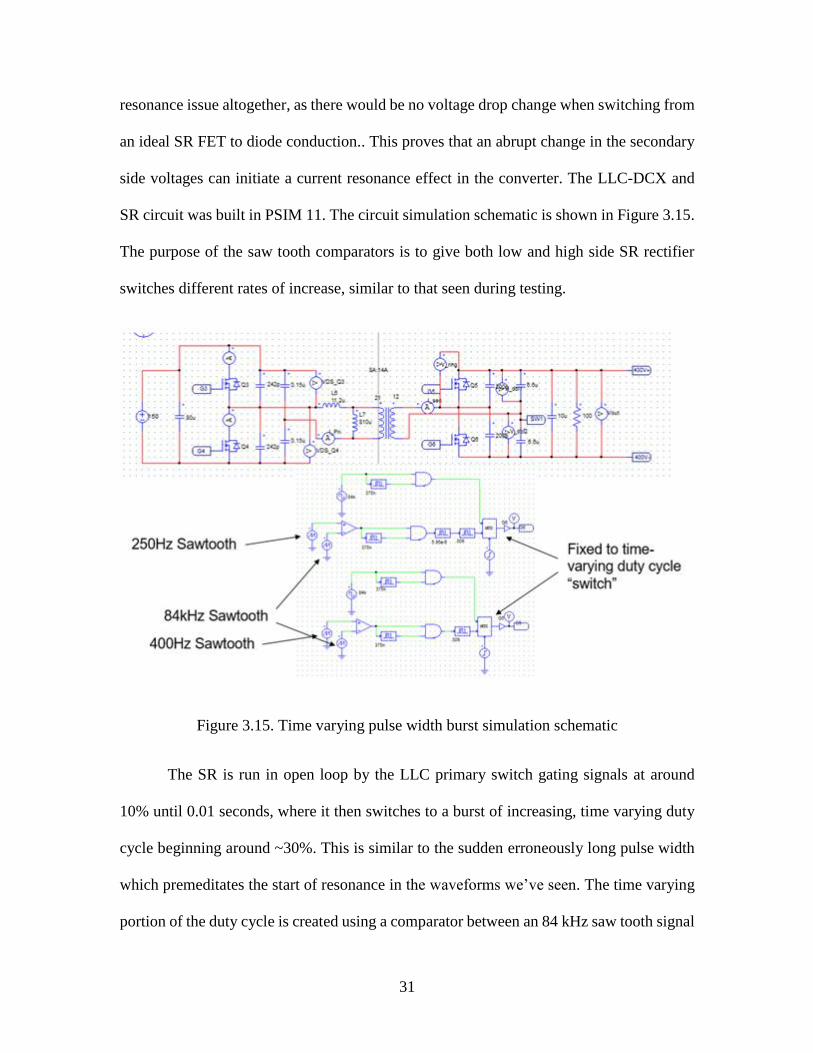
SR circuit was built in PSIM 11. The circuit simulation schematic is shown in Figure 3.15.
The purpose of the saw tooth comparators is to give both low and high side SR rectifier
switches different rates of increase, similar to that seen during testing.
Figure 3.15. Time varying pulse width burst simulation schematic
The SR is run in open loop by the LLC primary switch gating signals at around
10% until 0.01 seconds, where it then switches to a burst of increasing, time varying duty
cycle beginning around ~30%. This is similar to the sudden erroneously long pulse width
which premeditates the start of resonance in the waveforms we’ve seen. The time varying
portion of the duty cycle is created using a comparator between an 84 kHz saw tooth signal
32
generator and a slower, 400 Hz and 250 Hz saw tooth signal. The high and low side SR
signals are both arbitrarily increasing at different rates to emulate real world differences,
though the issue still occurs when both gate signals are increasing at the same rate over
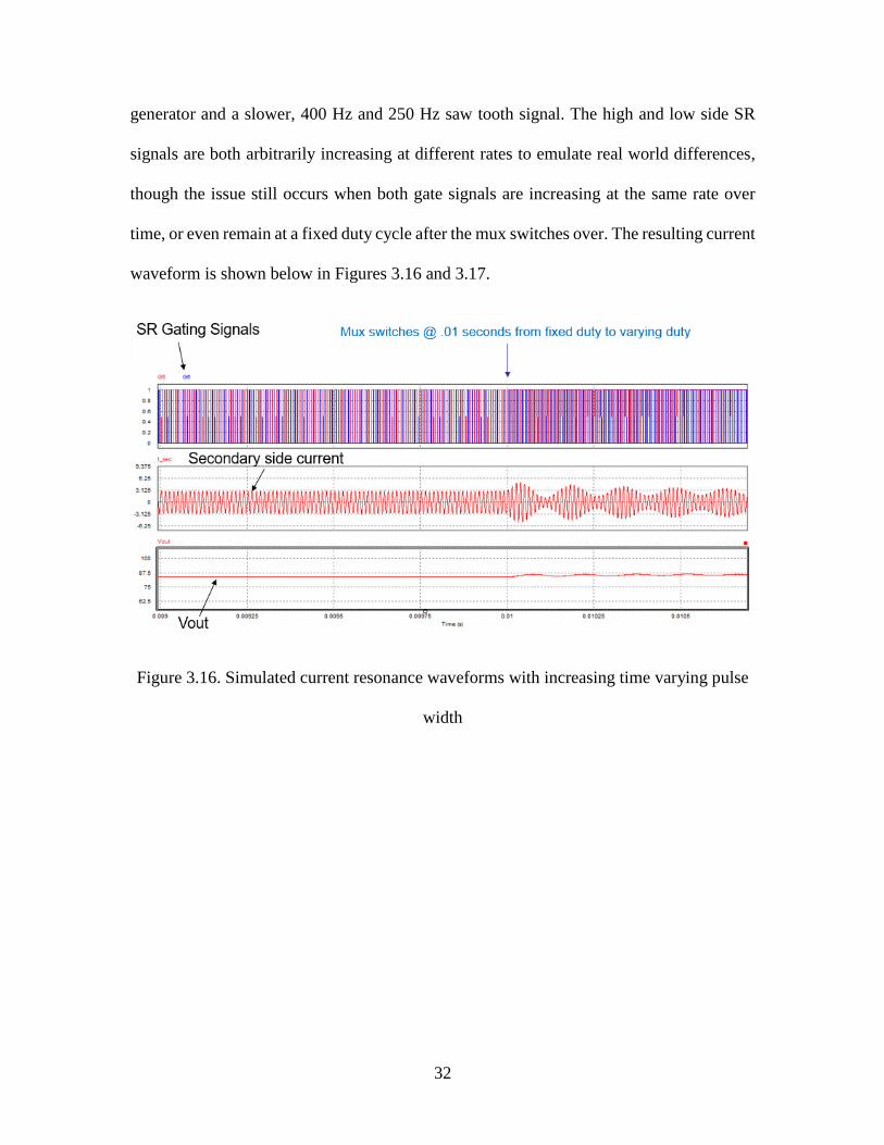
time, or even remain at a fixed duty cycle after the mux switches over. The resulting current
waveform is shown below in Figures 3.16 and 3.17.
Figure 3.16. Simulated current resonance waveforms with increasing time varying pulse
width
33
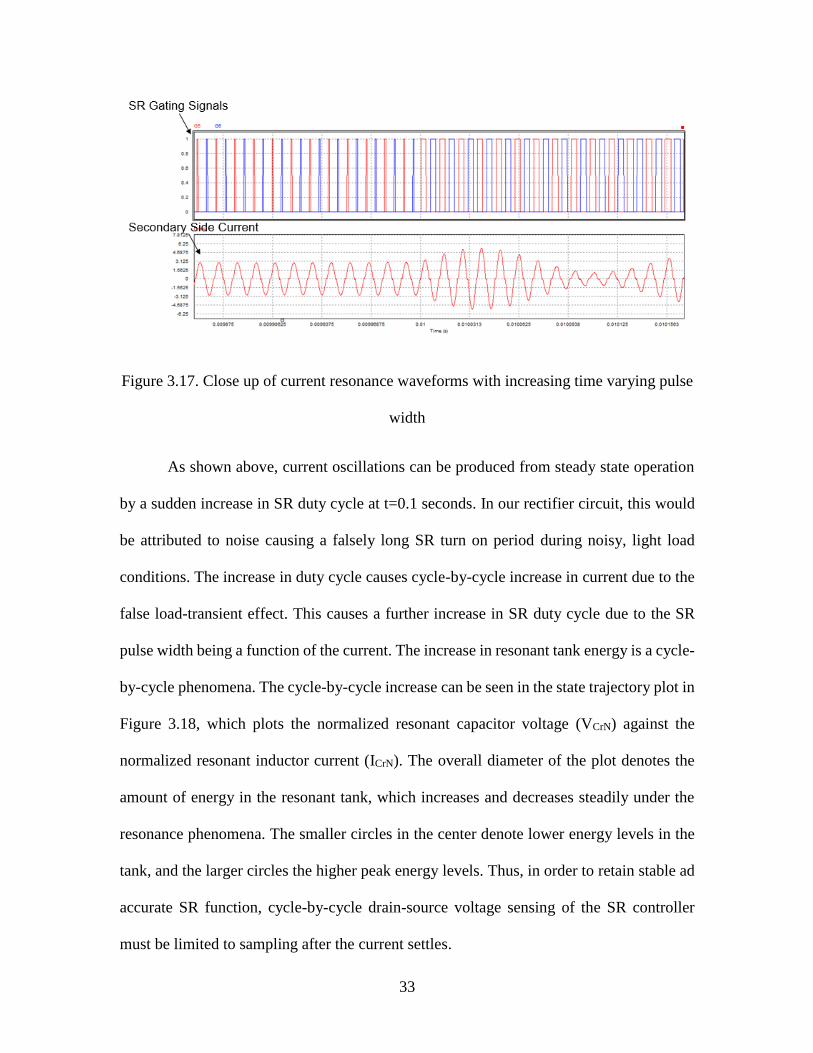
Figure 3.17. Close up of current resonance waveforms with increasing time varying pulse
width
As shown above, current oscillations can be produced from steady state operation
by a sudden increase in SR duty cycle at t=0.1 seconds. In our rectifier circuit, this would
be attributed to noise causing a falsely long SR turn on period during noisy, light load
conditions. The increase in duty cycle causes cycle-by-cycle increase in current due to the
false load-transient effect. This causes a further increase in SR duty cycle due to the SR
pulse width being a function of the current. The increase in resonant tank energy is a cycle-
by-cycle phenomena. The cycle-by-cycle increase can be seen in the state trajectory plot in
Figure 3.18, which plots the normalized resonant capacitor voltage (VCrN) against the
normalized resonant inductor current (ICrN). The overall diameter of the plot denotes the
amount of energy in the resonant tank, which increases and decreases steadily under the
resonance phenomena. The smaller circles in the center denote lower energy levels in the
tank, and the larger circles the higher peak energy levels. Thus, in order to retain stable ad
accurate SR function, cycle-by-cycle drain-source voltage sensing of the SR controller
must be limited to sampling after the current settles.
34
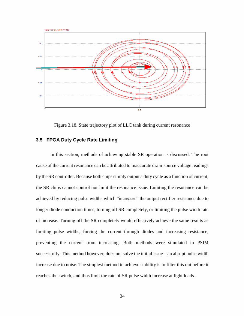
Figure 3.18. State trajectory plot of LLC tank during current resonance
3.5 FPGA Duty Cycle Rate Limiting
In this section, methods of achieving stable SR operation is discussed. The root
cause of the current resonance can be attributed to inaccurate drain-source voltage readings
by the SR controller. Because both chips simply output a duty cycle as a function of current,
the SR chips cannot control nor limit the resonance issue. Limiting the resonance can be
achieved by reducing pulse widths which “increases” the output rectifier resistance due to
longer diode conduction times, turning off SR completely, or limiting the pulse width rate
of increase. Turning off the SR completely would effectively achieve the same results as
limiting pulse widths, forcing the current through diodes and increasing resistance,
preventing the current from increasing. Both methods were simulated in PSIM
successfully. This method however, does not solve the initial issue – an abrupt pulse width
increase due to noise. The simplest method to achieve stability is to filter this out before it
reaches the switch, and thus limit the rate of SR pulse width increase at light loads.
35
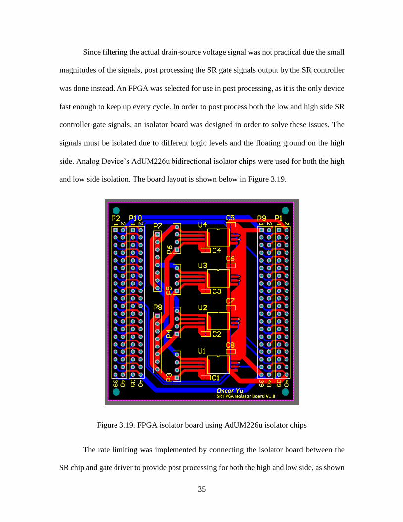
Since filtering the actual drain-source voltage signal was not practical due the small
magnitudes of the signals, post processing the SR gate signals output by the SR controller
was done instead. An FPGA was selected for use in post processing, as it is the only device
fast enough to keep up every cycle. In order to post process both the low and high side SR
controller gate signals, an isolator board was designed in order to solve these issues. The
signals must be isolated due to different logic levels and the floating ground on the high
side. Analog Device’s AdUM226u bidirectional isolator chips were used for both the high
and low side isolation. The board layout is shown below in Figure 3.19.
Figure 3.19. FPGA isolator board using AdUM226u isolator chips
The rate limiting was implemented by connecting the isolator board between the
SR chip and gate driver to provide post processing for both the high and low side, as shown
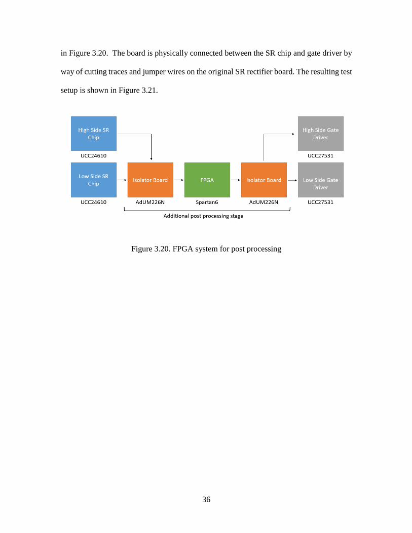
36
in Figure 3.20. The board is physically connected between the SR chip and gate driver by
way of cutting traces and jumper wires on the original SR rectifier board. The resulting test
setup is shown in Figure 3.21.
Figure 3.20. FPGA system for post processing
37
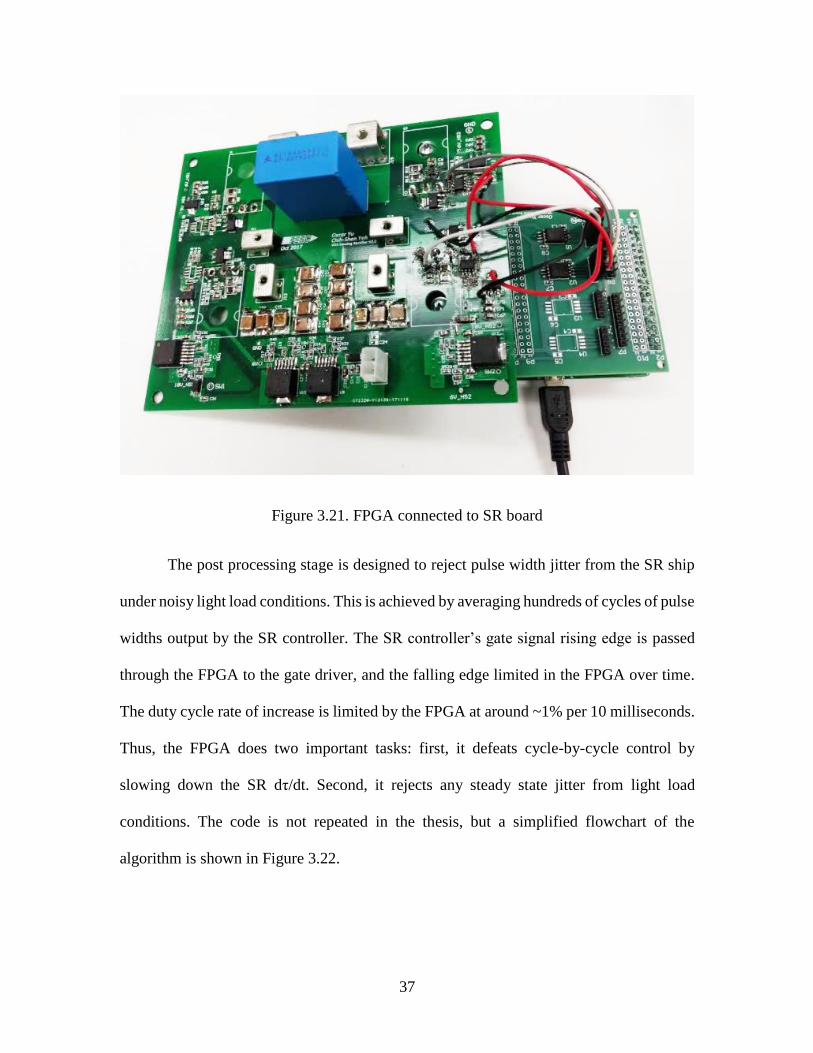
Figure 3.21. FPGA connected to SR board
The post processing stage is designed to reject pulse width jitter from the SR ship
under noisy light load conditions. This is achieved by averaging hundreds of cycles of pulse
widths output by the SR controller. The SR controller’s gate signal rising edge is passed
through the FPGA to the gate driver, and the falling edge limited in the FPGA over time.
The duty cycle rate of increase is limited by the FPGA at around ~1% per 10 milliseconds.
Thus, the FPGA does two important tasks: first, it defeats cycle-by-cycle control by
slowing down the SR dτ/dt. Second, it rejects any steady state jitter from light load
conditions. The code is not repeated in the thesis, but a simplified flowchart of the
algorithm is shown in Figure 3.22.
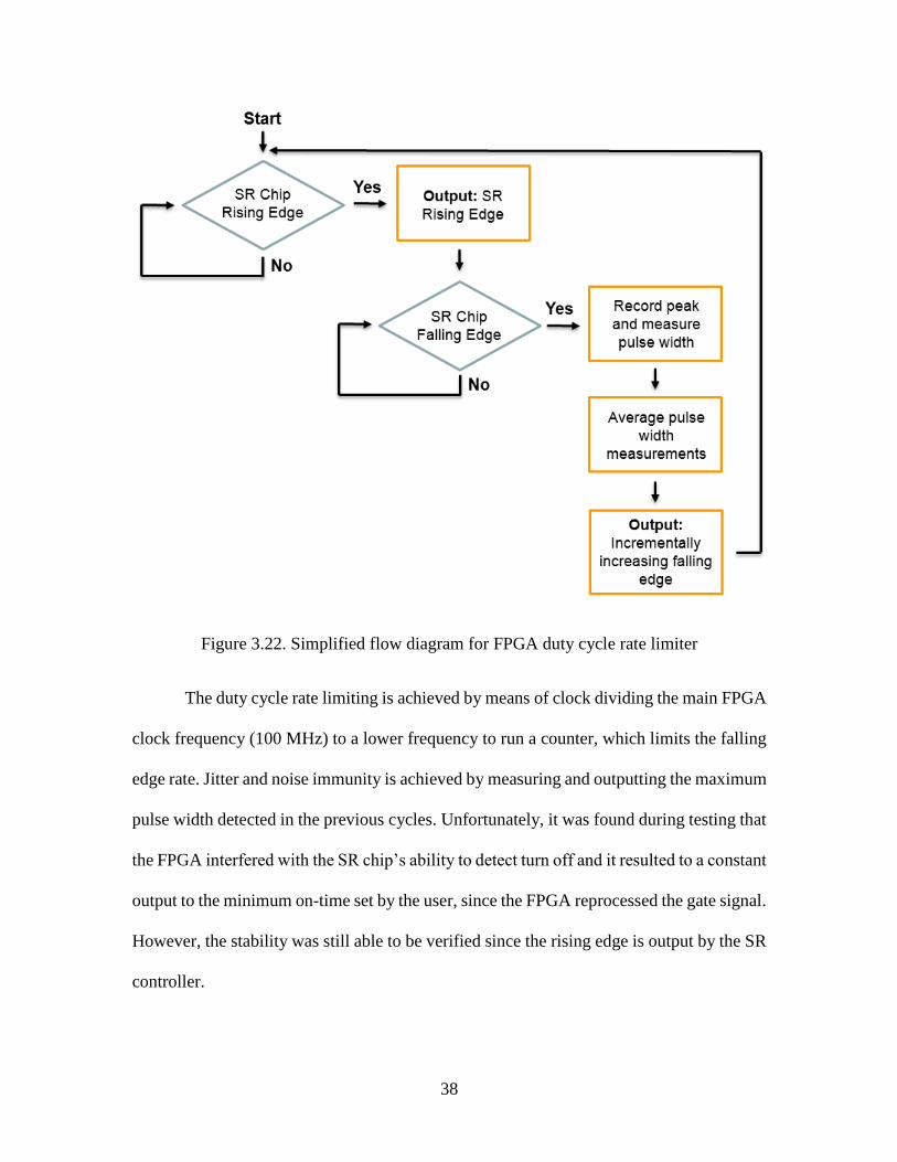
38
Figure 3.22. Simplified flow diagram for FPGA duty cycle rate limiter
The duty cycle rate limiting is achieved by means of clock dividing the main FPGA
clock frequency (100 MHz) to a lower frequency to run a counter, which limits the falling
edge rate. Jitter and noise immunity is achieved by measuring and outputting the maximum
pulse width detected in the previous cycles. Unfortunately, it was found during testing that
the FPGA interfered with the SR chip’s ability to detect turn off and it resulted to a constant
output to the minimum on-time set by the user, since the FPGA reprocessed the gate signal.
However, the stability was still able to be verified since the rising edge is output by the SR
controller.
39
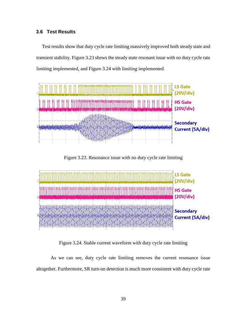
3.6 Test Results
Test results show that duty cycle rate limiting massively improved both steady state and
transient stability. Figure 3.23 shows the steady state resonant issue with no duty cycle rate
limiting implemented, and Figure 3.24 with limiting implemented.
Figure 3.23. Resonance issue with no duty cycle rate limiting
Figure 3.24. Stable current waveform with duty cycle rate limiting
As we can see, duty cycle rate limiting removes the current resonance issue
altogether. Furthermore, SR turn-on detection is much more consistent with duty cycle rate
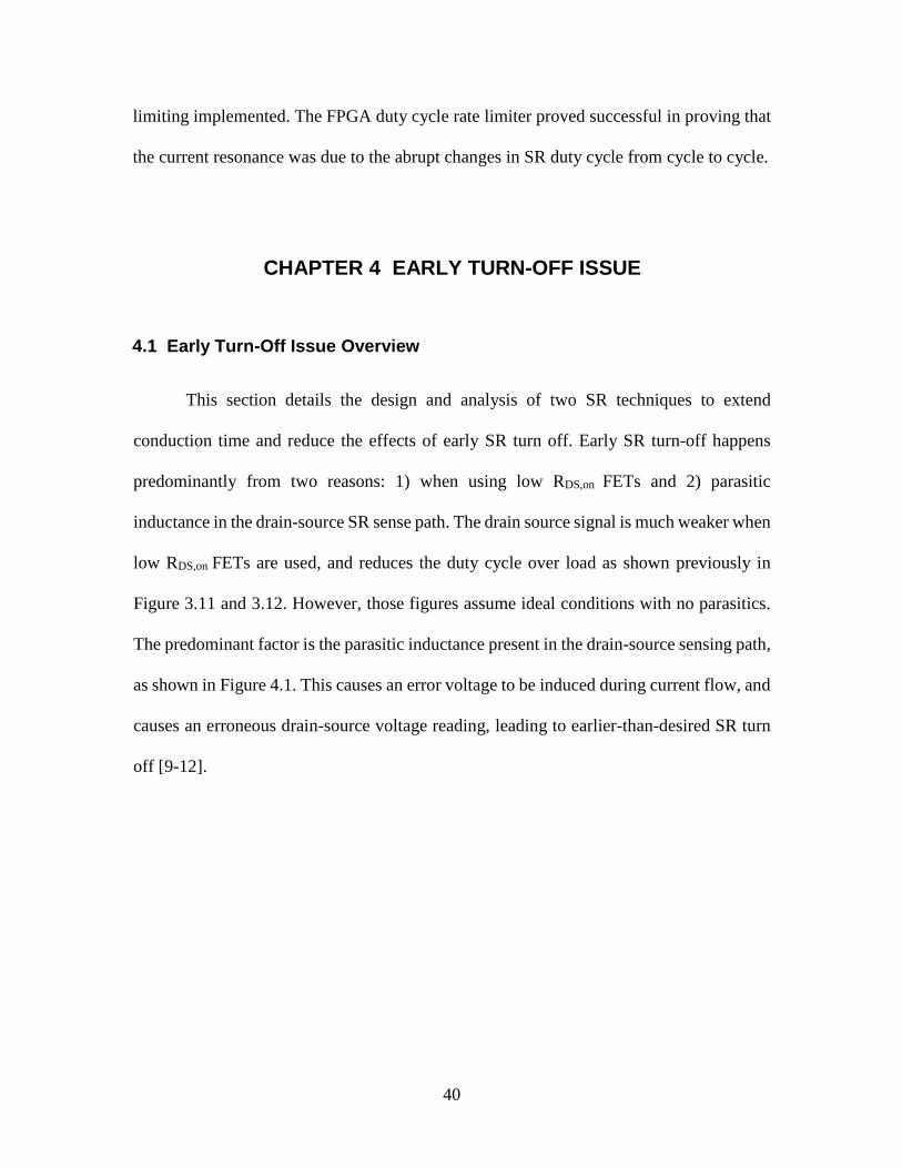
40
limiting implemented. The FPGA duty cycle rate limiter proved successful in proving that
the current resonance was due to the abrupt changes in SR duty cycle from cycle to cycle.
CHAPTER 4 EARLY TURN-OFF ISSUE
4.1 Early Turn-Off Issue Overview
This section details the design and analysis of two SR techniques to extend
conduction time and reduce the effects of early SR turn off. Early SR turn-off happens
predominantly from two reasons: 1) when using low RDS,on FETs and 2) parasitic
inductance in the drain-source SR sense path. The drain source signal is much weaker when
low RDS,on FETs are used, and reduces the duty cycle over load as shown previously in
Figure 3.11 and 3.12. However, those figures assume ideal conditions with no parasitics.
The predominant factor is the parasitic inductance present in the drain-source sensing path,
as shown in Figure 4.1. This causes an error voltage to be induced during current flow, and
causes an erroneous drain-source voltage reading, leading to earlier-than-desired SR turn
off [9-12].
41
Figure 4.1. Parasitic inductance in drain-source SR sense path
The result of these turn-off issues is shown in Figure 3.2, where the SR FET used
(Rohm SCT3017) turns off much earlier than desired. This results in increased switching
and conduction loss, as current is redirected through the much lossier parallel diode. An
SR FET switched ideally would experience no switching loss, as turn-on and turn-off
conditions would both be near zero current.
Since the phase shift in the sensed drain-source voltage is a function of the parasitic
inductance Lp and SR FET RDS,on, the impact of the parasitic inductance can be minimized
with greater SR FET RDS,on as we can see from the equation below [9,13]. Thus, the sensed
voltage can be varied if the channel resistance can be dynamically modulated.
𝑉𝑑𝑠,𝑠𝑒𝑛𝑠𝑒𝑑(𝑡) = −𝜋
2[
𝑉𝑜
𝑅𝐿] sin (2𝜋𝑓𝑠𝑡 + arctan (
2𝜋𝑓𝑠𝐿𝑝
𝑅𝐷𝑆,𝑜𝑛)) ∗ |𝑅𝐷𝑆,𝑜𝑛 + 𝑗2𝜋𝑓𝑠𝐿𝑝|
42
4.2 Sequential Parallel Switching Introduction
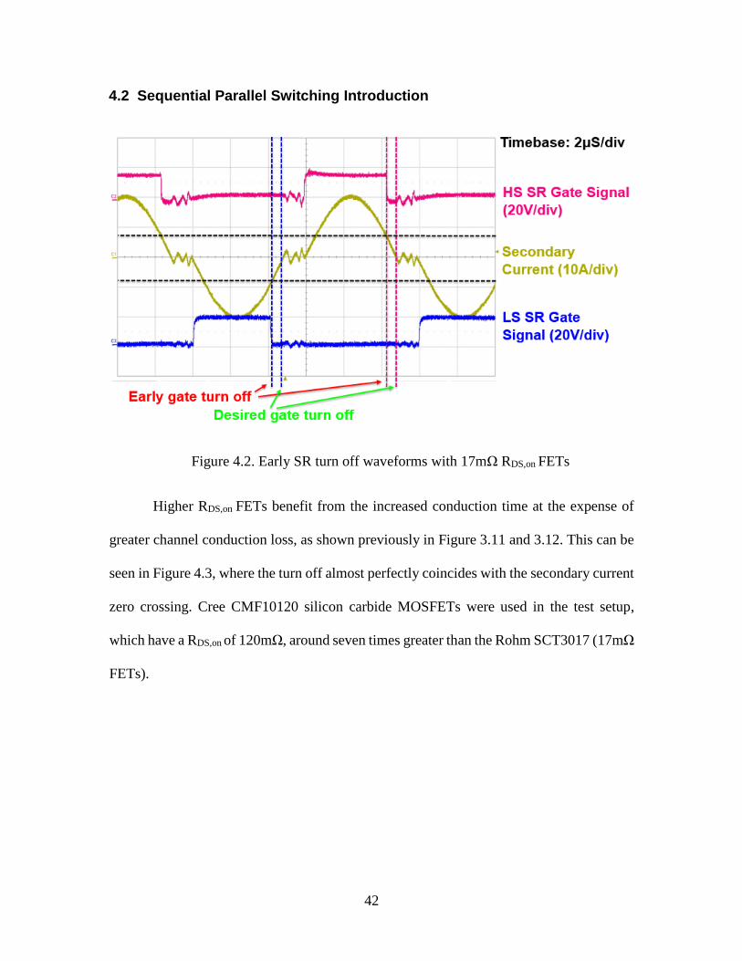
Figure 4.2. Early SR turn off waveforms with 17mΩ RDS,on FETs
Higher RDS,on FETs benefit from the increased conduction time at the expense of
greater channel conduction loss, as shown previously in Figure 3.11 and 3.12. This can be
seen in Figure 4.3, where the turn off almost perfectly coincides with the secondary current
zero crossing. Cree CMF10120 silicon carbide MOSFETs were used in the test setup,
which have a RDS,on of 120mΩ, around seven times greater than the Rohm SCT3017 (17mΩ
FETs).
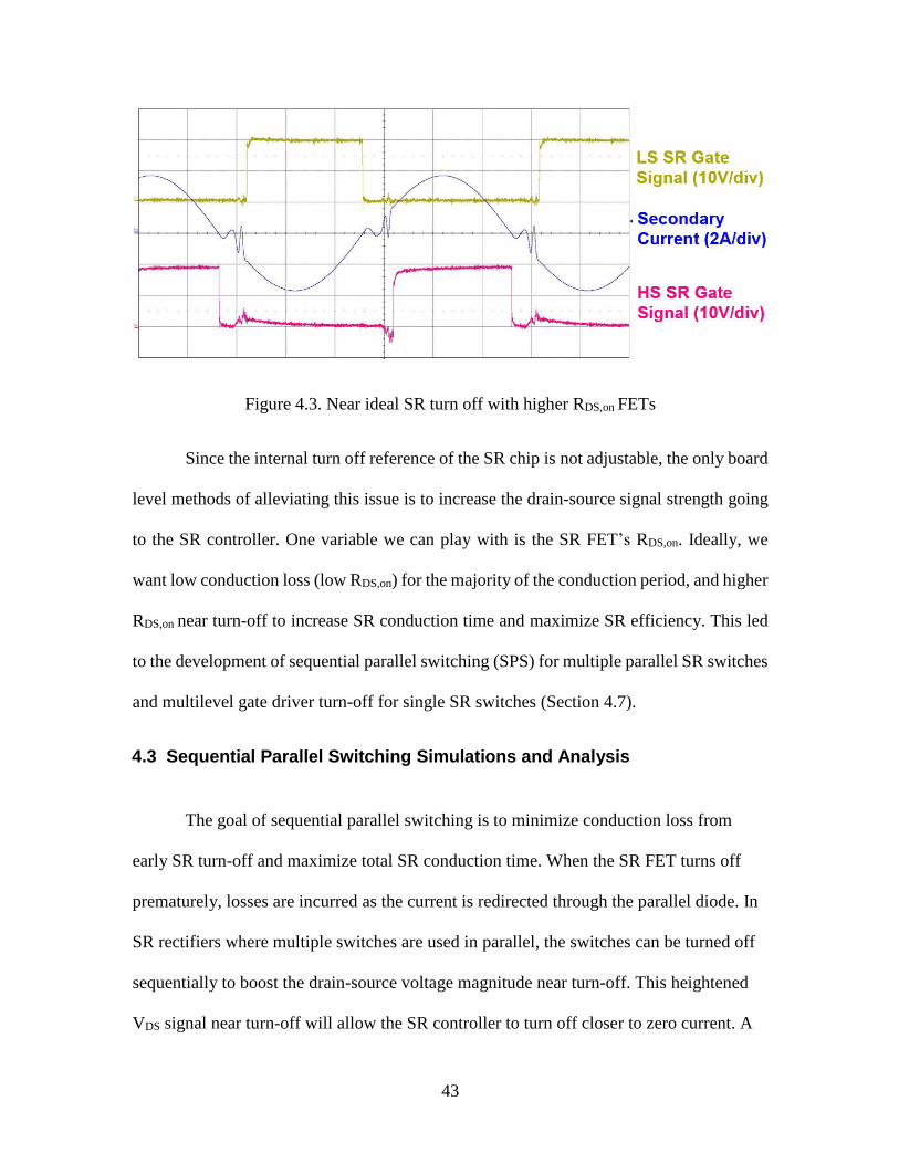
43
Figure 4.3. Near ideal SR turn off with higher RDS,on FETs
Since the internal turn off reference of the SR chip is not adjustable, the only board
level methods of alleviating this issue is to increase the drain-source signal strength going
to the SR controller. One variable we can play with is the SR FET’s RDS,on. Ideally, we
want low conduction loss (low RDS,on) for the majority of the conduction period, and higher
RDS,on near turn-off to increase SR conduction time and maximize SR efficiency. This led
to the development of sequential parallel switching (SPS) for multiple parallel SR switches
and multilevel gate driver turn-off for single SR switches (Section 4.7).
4.3 Sequential Parallel Switching Simulations and Analysis
The goal of sequential parallel switching is to minimize conduction loss from
early SR turn-off and maximize total SR conduction time. When the SR FET turns off
prematurely, losses are incurred as the current is redirected through the parallel diode. In
SR rectifiers where multiple switches are used in parallel, the switches can be turned off
sequentially to boost the drain-source voltage magnitude near turn-off. This heightened
VDS signal near turn-off will allow the SR controller to turn off closer to zero current. A
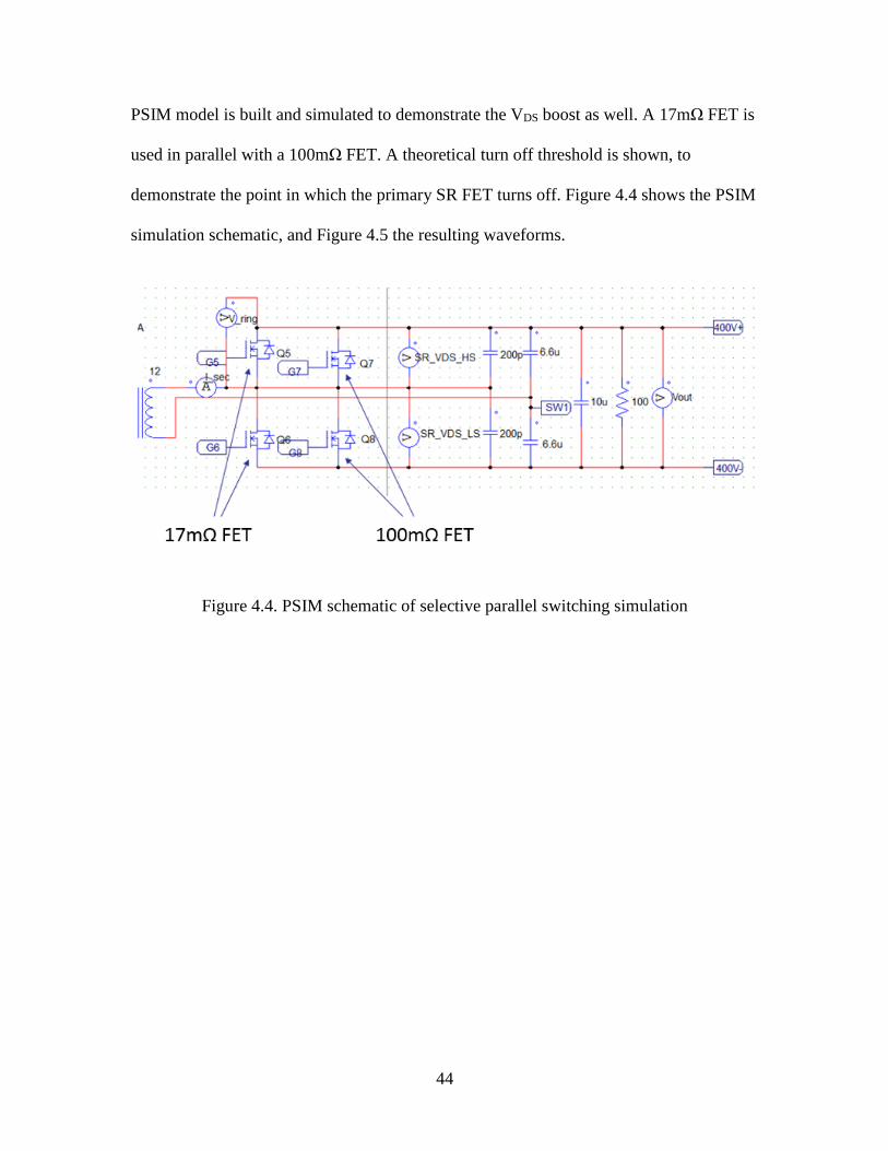
44
PSIM model is built and simulated to demonstrate the VDS boost as well. A 17mΩ FET is
used in parallel with a 100mΩ FET. A theoretical turn off threshold is shown, to
demonstrate the point in which the primary SR FET turns off. Figure 4.4 shows the PSIM
simulation schematic, and Figure 4.5 the resulting waveforms.
Figure 4.4. PSIM schematic of selective parallel switching simulation
45
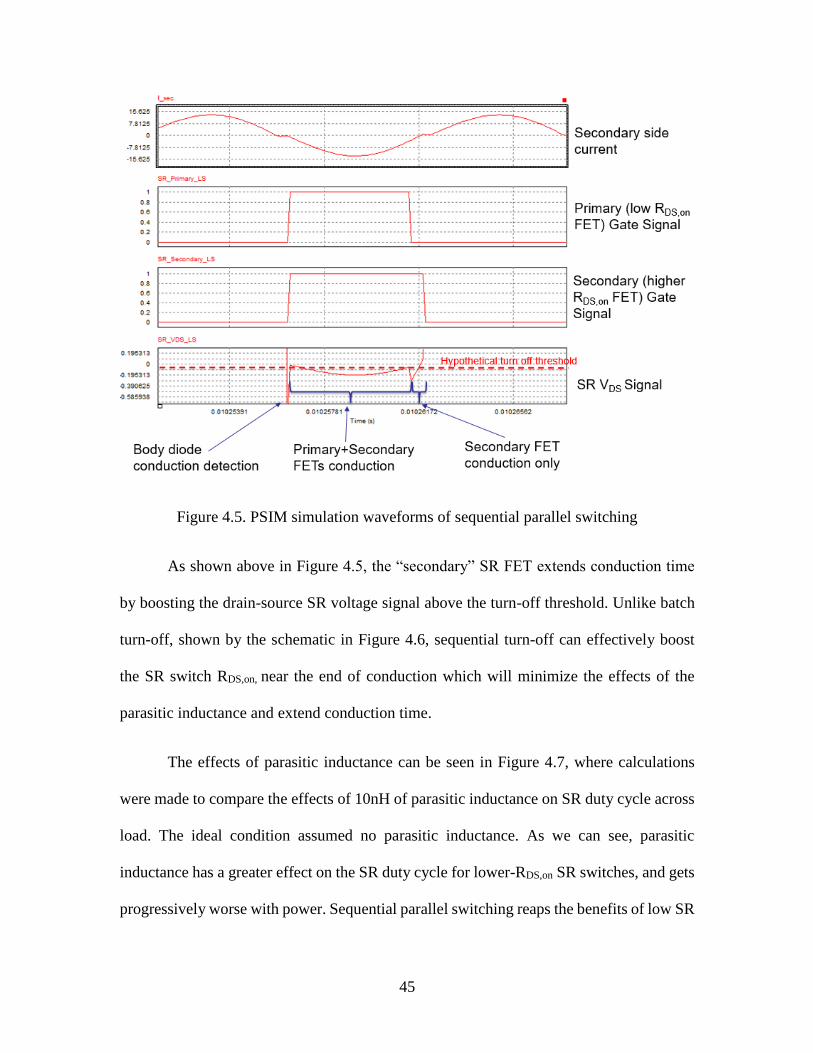
Figure 4.5. PSIM simulation waveforms of sequential parallel switching
As shown above in Figure 4.5, the “secondary” SR FET extends conduction time
by boosting the drain-source SR voltage signal above the turn-off threshold. Unlike batch
turn-off, shown by the schematic in Figure 4.6, sequential turn-off can effectively boost
the SR switch RDS,on, near the end of conduction which will minimize the effects of the
parasitic inductance and extend conduction time.
The effects of parasitic inductance can be seen in Figure 4.7, where calculations
were made to compare the effects of 10nH of parasitic inductance on SR duty cycle across
load. The ideal condition assumed no parasitic inductance. As we can see, parasitic
inductance has a greater effect on the SR duty cycle for lower-RDS,on SR switches, and gets
progressively worse with power. Sequential parallel switching reaps the benefits of low SR
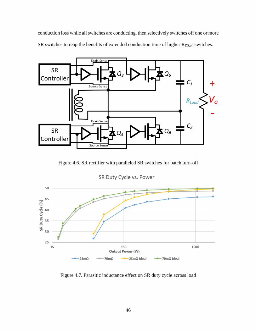
46
conduction loss while all switches are conducting, then selectively switches off one or more
SR switches to reap the benefits of extended conduction time of higher RDS,on switches.
Figure 4.6. SR rectifier with paralleled SR switches for batch turn-off
Figure 4.7. Parasitic inductance effect on SR duty cycle across load
47
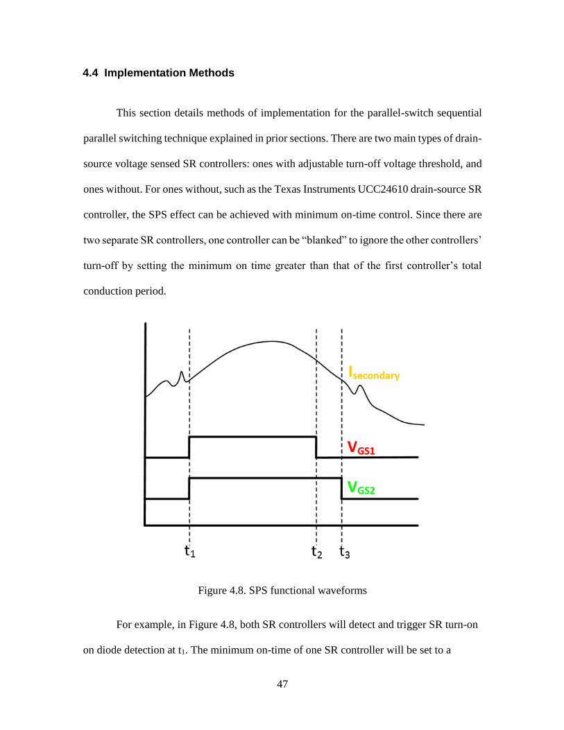
4.4 Implementation Methods
This section details methods of implementation for the parallel-switch sequential
parallel switching technique explained in prior sections. There are two main types of drain-
source voltage sensed SR controllers: ones with adjustable turn-off voltage threshold, and
ones without. For ones without, such as the Texas Instruments UCC24610 drain-source SR
controller, the SPS effect can be achieved with minimum on-time control. Since there are
two separate SR controllers, one controller can be “blanked” to ignore the other controllers’
turn-off by setting the minimum on time greater than that of the first controller’s total
conduction period.
Figure 4.8. SPS functional waveforms
For example, in Figure 4.8, both SR controllers will detect and trigger SR turn-on
on diode detection at t1. The minimum on-time of one SR controller will be set to a
48
period less than that of drain-source voltage sensed batch turn off, t2. The second SR
controller will be set to a minimum-on time greater than that of the total conduction
period of the first controller, a minimum-on time greater than t2 but less than t3. A
minimum-on time greater or equal to t3 would not allow for the SR controller to correctly
sense turn-off. This method faces one main issue – the dynamics in current waveforms as
the load changes. Thus, this method is only practical for implementation on systems with
a relatively fixed load. SR controllers with adjustable turn-off voltage thresholds offer
greater flexibility, as described below.
For controllers with adjustable turn-off voltage thresholds, like the ON
Semiconductor NCP4303 SR controller, SPS is very simple to implement across load.
The turn-off voltage for one controller is set lower than the other controller. The end
result can be seen in Figure 4.9. Since the turn-off thresholds are adjustable, the
resolution in which the first and second controller turn-off the gate signal can be finely
adjusted. This allows for maximum conduction time with all switches on before shutting
others off, maximizing SR efficiency.
49
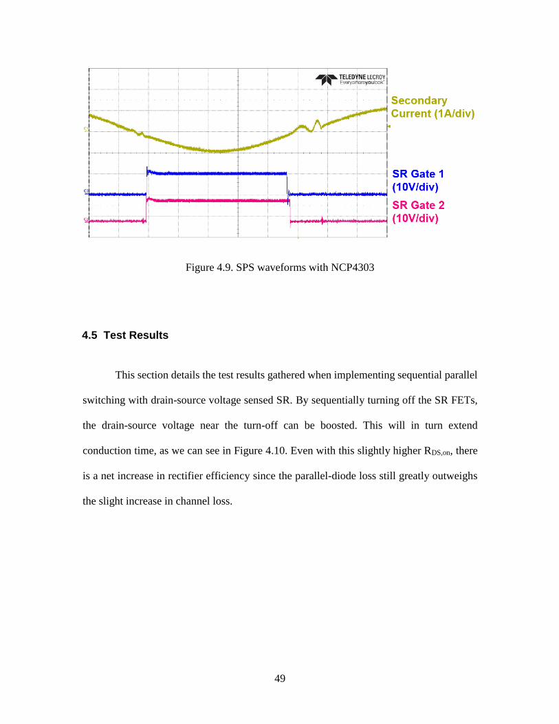
Figure 4.9. SPS waveforms with NCP4303
4.5 Test Results
This section details the test results gathered when implementing sequential parallel
switching with drain-source voltage sensed SR. By sequentially turning off the SR FETs,
the drain-source voltage near the turn-off can be boosted. This will in turn extend
conduction time, as we can see in Figure 4.10. Even with this slightly higher RDS,on, there
is a net increase in rectifier efficiency since the parallel-diode loss still greatly outweighs
the slight increase in channel loss.
50
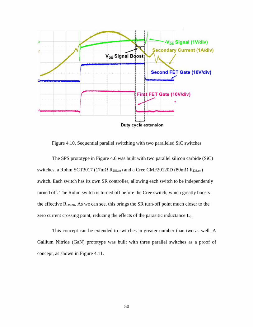
Figure 4.10. Sequential parallel switching with two paralleled SiC switches
The SPS prototype in Figure 4.6 was built with two parallel silicon carbide (SiC)
switches, a Rohm SCT3017 (17mΩ RDS,on) and a Cree CMF20120D (80mΩ RDS,on)
switch. Each switch has its own SR controller, allowing each switch to be independently
turned off. The Rohm switch is turned off before the Cree switch, which greatly boosts
the effective RDS,on. As we can see, this brings the SR turn-off point much closer to the
zero current crossing point, reducing the effects of the parasitic inductance Lp.
This concept can be extended to switches in greater number than two as well. A
Gallium Nitride (GaN) prototype was built with three parallel switches as a proof of
concept, as shown in Figure 4.11.

51
Figure 4.11. TI GaN SPS test board with three LMG3410-EVM modules
SPS is implemented only on the low side, for stability. Two TI UCC24610 drain-
source SR controllers are used, one controlling two modules, and the other controlling a
single module. With all three modules on, there was a combined RDS,on of 23mΩ. With only
one module conducting, there is an RDS,on of 70mΩ. Testing showed successful
implementation of SPS, as shown in Figure 4.12. At light load, the total SR conduction
time is greatly extended with SPS rather than batch turn-off.
52
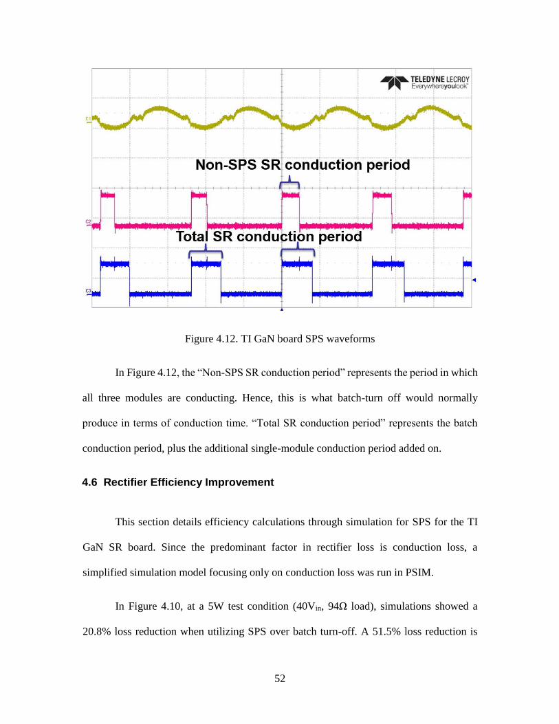
Figure 4.12. TI GaN board SPS waveforms
In Figure 4.12, the “Non-SPS SR conduction period” represents the period in which
all three modules are conducting. Hence, this is what batch-turn off would normally
produce in terms of conduction time. “Total SR conduction period” represents the batch
conduction period, plus the additional single-module conduction period added on.
4.6 Rectifier Efficiency Improvement
This section details efficiency calculations through simulation for SPS for the TI
GaN SR board. Since the predominant factor in rectifier loss is conduction loss, a
simplified simulation model focusing only on conduction loss was run in PSIM.
In Figure 4.10, at a 5W test condition (40Vin, 94Ω load), simulations showed a
20.8% loss reduction when utilizing SPS over batch turn-off. A 51.5% loss reduction is
53
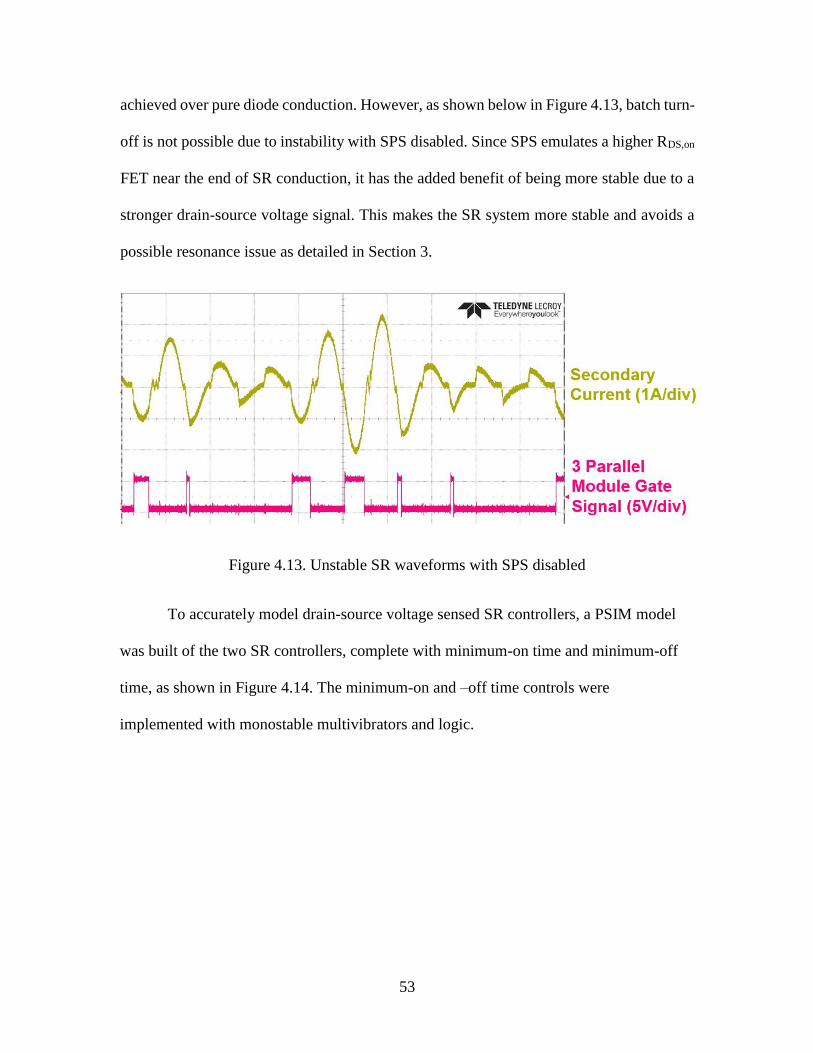
achieved over pure diode conduction. However, as shown below in Figure 4.13, batch turn-
off is not possible due to instability with SPS disabled. Since SPS emulates a higher RDS,on
FET near the end of SR conduction, it has the added benefit of being more stable due to a
stronger drain-source voltage signal. This makes the SR system more stable and avoids a
possible resonance issue as detailed in Section 3.
Figure 4.13. Unstable SR waveforms with SPS disabled
To accurately model drain-source voltage sensed SR controllers, a PSIM model
was built of the two SR controllers, complete with minimum-on time and minimum-off
time, as shown in Figure 4.14. The minimum-on and –off time controls were
implemented with monostable multivibrators and logic.
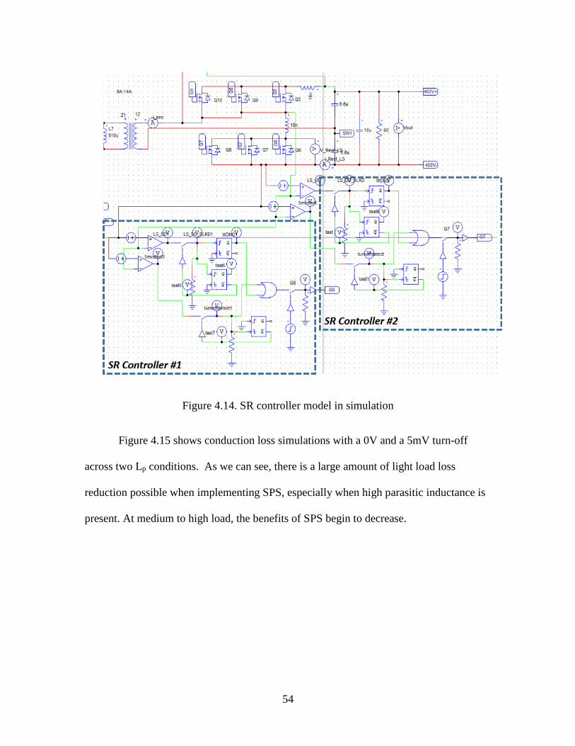
54
Figure 4.14. SR controller model in simulation
Figure 4.15 shows conduction loss simulations with a 0V and a 5mV turn-off
across two Lp conditions. As we can see, there is a large amount of light load loss
reduction possible when implementing SPS, especially when high parasitic inductance is
present. At medium to high load, the benefits of SPS begin to decrease.
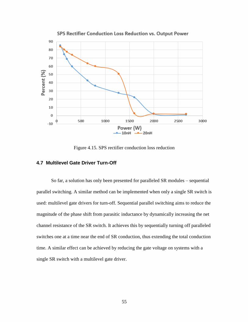
55
Figure 4.15. SPS rectifier conduction loss reduction
4.7 Multilevel Gate Driver Turn-Off
So far, a solution has only been presented for paralleled SR modules – sequential
parallel switching. A similar method can be implemented when only a single SR switch is
used: multilevel gate drivers for turn-off. Sequential parallel switching aims to reduce the
magnitude of the phase shift from parasitic inductance by dynamically increasing the net
channel resistance of the SR switch. It achieves this by sequentially turning off paralleled
switches one at a time near the end of SR conduction, thus extending the total conduction
time. A similar effect can be achieved by reducing the gate voltage on systems with a
single SR switch with a multilevel gate driver.
56
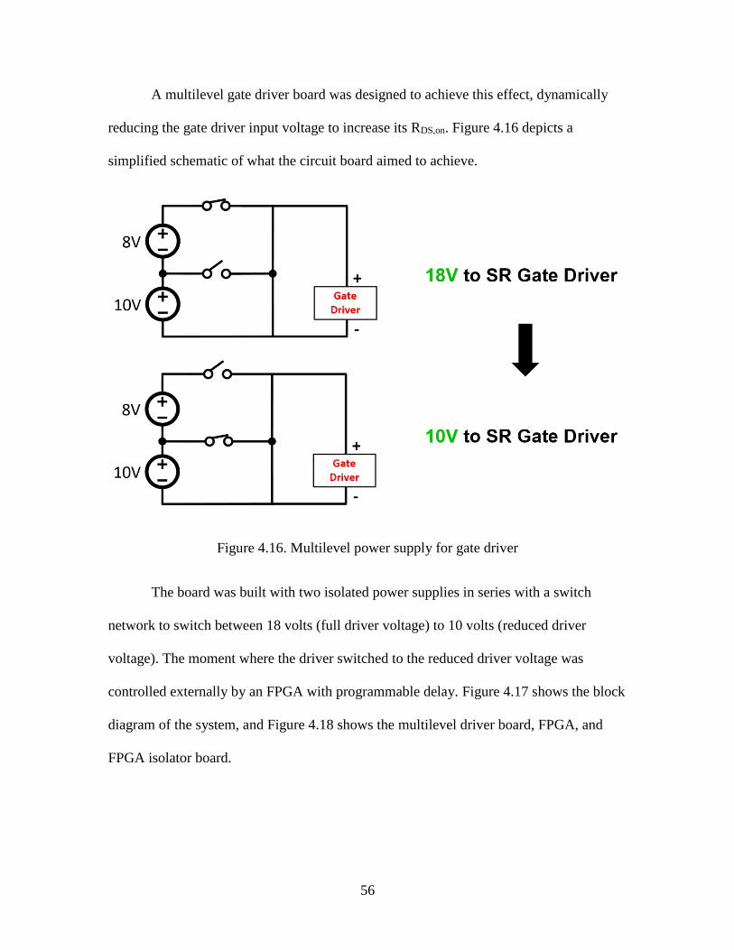
A multilevel gate driver board was designed to achieve this effect, dynamically
reducing the gate driver input voltage to increase its RDS,on. Figure 4.16 depicts a
simplified schematic of what the circuit board aimed to achieve.
Figure 4.16. Multilevel power supply for gate driver
The board was built with two isolated power supplies in series with a switch
network to switch between 18 volts (full driver voltage) to 10 volts (reduced driver
voltage). The moment where the driver switched to the reduced driver voltage was
controlled externally by an FPGA with programmable delay. Figure 4.17 shows the block
diagram of the system, and Figure 4.18 shows the multilevel driver board, FPGA, and
FPGA isolator board.
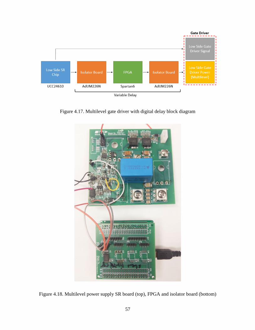
57
Figure 4.17. Multilevel gate driver with digital delay block diagram
Figure 4.18. Multilevel power supply SR board (top), FPGA and isolator board (bottom)
58
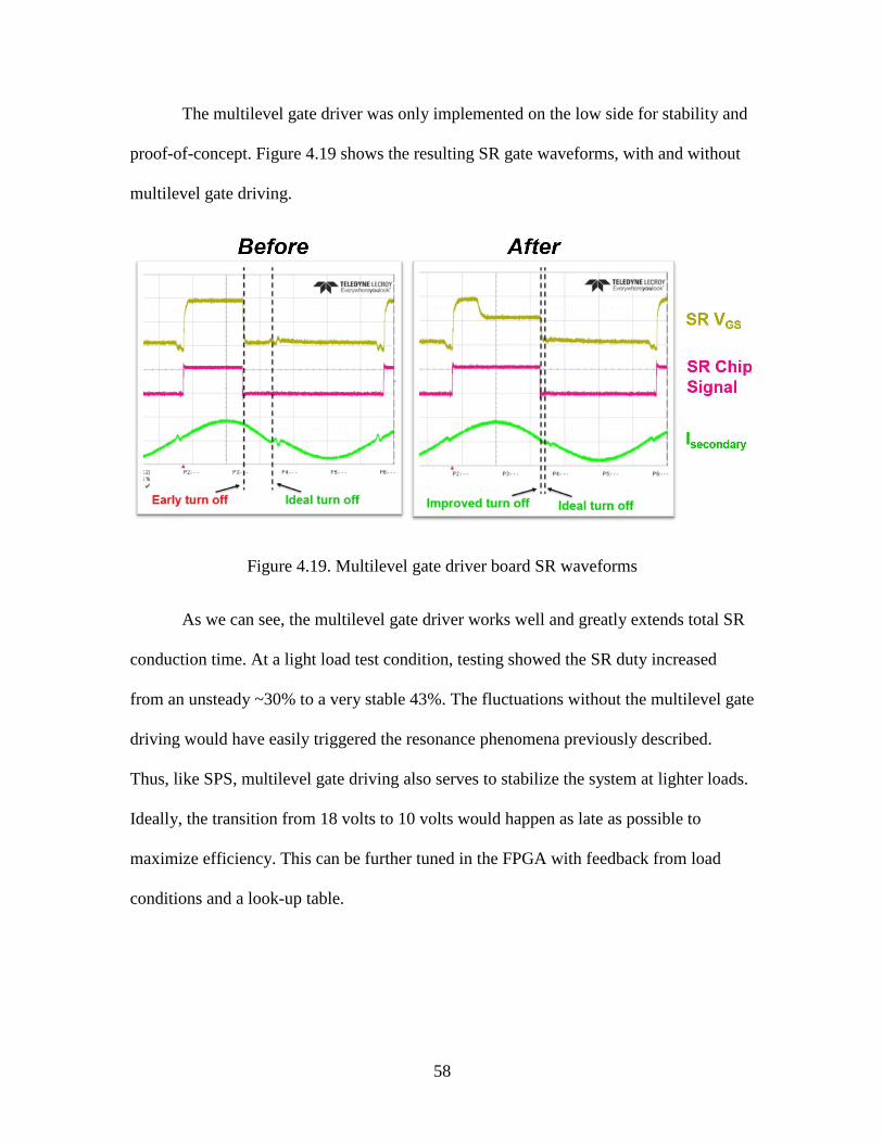
The multilevel gate driver was only implemented on the low side for stability and
proof-of-concept. Figure 4.19 shows the resulting SR gate waveforms, with and without
multilevel gate driving.
Figure 4.19. Multilevel gate driver board SR waveforms
As we can see, the multilevel gate driver works well and greatly extends total SR
conduction time. At a light load test condition, testing showed the SR duty increased
from an unsteady ~30% to a very stable 43%. The fluctuations without the multilevel gate
driving would have easily triggered the resonance phenomena previously described.
Thus, like SPS, multilevel gate driving also serves to stabilize the system at lighter loads.
Ideally, the transition from 18 volts to 10 volts would happen as late as possible to
maximize efficiency. This can be further tuned in the FPGA with feedback from load
conditions and a look-up table.
59
CHAPTER 5 CONCLUSION AND FUTURE WORK
In the first half of this thesis, a current resonance issue is discovered, investigated,
simulated, and a solution is proposed in the form of a FPGA duty cycle rate limiter. In the
second half, an early SR turn off issue is reviewed, simulated, and two solutions proposed:
sequential parallel switching, and multilevel gate driving. Methods of implementation were
discussed, simulations run for efficiency, and both solutions were successfully validated at
the board level. The major contributions of this thesis are the discovery of the light load
resonance issue, and the techniques to extend conduction time.
Future work includes a deeper look into multilevel gate driving for high power
applications, where SR is becoming more desirable, as well as a much more detailed loss
analysis. Efforts into full implementation on both low and high sides will follow, as well
as a deeper look into higher frequency operation.
60
REFERENCES
[1] J. S. Lai, J. M. Choe, C. S. Yeh, S. R. Moon, W. H. Lai and L. Zhang, "A modular
front-end medium-voltage solid-state transformer," 2017 Asian Conference on Energy,
Power and Transportation Electrification (ACEPT), Singapore, 2017, pp. 1-6.
[2] J. S. Lai, W. H. Lai, S. R. Moon, L. Zhang and A. Maitra, "A 15-kV class intelligent
universal transformer for utility applications," 2016 IEEE Applied Power Electronics
Conference and Exposition (APEC), Long Beach, CA, 2016, pp. 1974-1981.
[3] Abdel-Rahman, S. (2008). An introduction to LLC resonant half-bridge converter.
[ebook] STMicroelectronics Application Note, pp.1-11. Available at:
http://www.st.com/content/ccc/resource/technical/document/application_note/de/f9/17/b7
/ad/9f/4d/dd/CD00174208.pdf/files/CD00174208.pdf/jcr:content/translations/en.CD0017
4208.pdf [Accessed 23 Feb. 2018].
[4] D. Wang, L. Jia, Y. F. Liu and P. C. Sen, "An improved driving method for synchronous
rectifier using drain-source voltage sensing," 2011 Twenty-Sixth Annual IEEE Applied
Power Electronics Conference and Exposition (APEC), Fort Worth, TX, 2011, pp. 1433-
1438.
[5] M. S. Amouzandeh, B. Mahdavikhah, A. Prodic and B. McDonald, "Digital
synchronous rectification controller for llc resonant converters," 2016 IEEE Applied Power
Electronics Conference and Exposition (APEC), Long Beach, CA, 2016, pp. 329-333.
[6] J. Wang and B. Lu, "Open loop synchronous rectifier driver for LLC resonant
converter," 2013 Twenty-Eighth Annual IEEE Applied Power Electronics Conference and
Exposition (APEC), Long Beach, CA, 2013, pp.2048-2051.
[7] Texas Instruments, “UCC24610 GREEN Rectifier™ Controller Device” Texas
Instruments, Dallas, TX, USA, October 2015. [Online]. Available:
http://www.ti.com/lit/ds/symlink/ucc24610.pdf
[8] ON Semiconductor, “NCP4303A, NCP4303B Secondary Side Synchronous
Rectification Driver for High Efficiency SMPS Topologies” ON Semiconductor, Denver,
CO, USA, April 2015. [Online]. Available:
https://www.onsemi.com/pub/Collateral/NCP4303-D.PDF
[9] D. Fu, Y. Liu, F. C. Lee and M. Xu, "A Novel Driving Scheme for Synchronous
Rectifiers in LLC Resonant Converters," in IEEE Transactions on Power Electronics, vol.
24, no. 5, pp. 1321-1329, May 2009.
[10] D. Fu, B. Lu and F. C. Lee, "1MHz High Efficiency LLC Resonant Converters with
Synchronous Rectifier," 2007 IEEE Power Electronics Specialists Conference, Orlando,
FL, 2007, pp. 2404-2410.
[11] C. Fei, F. C. Lee and Q. Li, "Digital implementation of adaptive synchronous rectifier
(SR) driving scheme for LLC resonant converters," 2016 IEEE Applied Power Electronics
Conference and Exposition (APEC), Long Beach, CA, 2016, pp. 322-328.
[12] Dianbo Fu, Ya Liu, F. C. Lee and Ming Xu, "An improved novel driving scheme of
synchronous rectifiers for LLC resonant converters," 2008 Twenty-Third Annual IEEE
Applied Power Electronics Conference and Exposition, Austin, TX, 2008, pp. 510-516.
61
[13] Liu, Y. (2007). High Efficiency Optimization of LLC Resonant Converter for Wide
Load Range. Masters. Virginia Polytechnic Institute and State University.
[14] D. Wang, L. Jia, Y. Liu and P. C. Sen, "An improved driving method for synchronous
rectifier using drain-source voltage sensing," 2011 Twenty-Sixth Annual IEEE Applied
Power Electronics Conference and Exposition (APEC), Fort Worth, TX, 2011, pp. 1433-
1438.
[15] D. Fu, Y. Liu, F. C. Lee and M. Xu, "A Novel Driving Scheme for Synchronous
Rectifiers in LLC Resonant Converters," in IEEE Transactions on Power Electronics, vol.
24, no. 5, pp. 1321-1329, May 2009.