impact of intellectual property cores on field programmable gate array...
TRANSCRIPT

Impact of Intellectual Property CoresonField ProgrammableGateArray
Designs
by
LesleyShannon
A Thesissubmittedin conformitywith therequirementsfor theDegreeof Masterof AppliedSciencein the
Departmentof ElectricalandComputerEngineeringUniversityof Toronto
Copyright c�
2001by Lesley Shannon


Impact of Intellectual Property CoresonField ProgrammableGateArray
Designs
Lesley ShannonMasterof AppliedScience,
2001Departmentof ElectricalandComputerEngineering
Universityof Toronto
Abstract
IntellectualProperty(IP) designis a rapidly growing industryanddesignersandusers
arebeingchallengedto developinfrastructureandstandardinterfacesfor this new indus-
try. This researchstudiesthe impact that IntellectualPropertycoreshave on the design
of Systems-on-Chip(SoC) implementedon Field ProgrammableGateArrays (FPGAs).
To obtainanunderstandingof thecurrentstateof coretechnology, a systemwasbuilt us-
ing multiple IP cores. A corewasdesignedto learnaboutcoredesignissueswhile the
remainingcoreswereobtainedfrom vendors.
Theresultswereslightly discouragingasit is not a simpleprocessto incorporatethird
partycoresinto a design,nor wasit easyto obtaincoresfor thesystem.Still, theexperi-
encehasprovidedmuchinsightasto whatproblemsmustbeaddressedin theIP industryto
facilitatea designmethodologythatincludestheuseof IP. Thesechallengesincludebasic
concernssuchasinterfacingdifficultiesaswell asdocumentationproblemsthathavebeen
grosslyunderestimated.Yet the issueremains:circuitsarebecomingtoo complex to cus-
tom designandachieve thedesiredtime-to-market of a product;sohow canwe interface
IP from vendorsto asystemdesignin amethodicalandtimely fashion?
iii

Acknowledgements
I would like to thankmy supervisor, PaulChow, for hisunendingpatienceandwilling-
nessat any time to answerany of many questions-even if they werenot directly related
to my thesis. This hasbeena wonderful learningexperiencethat hasconvinced me to
continuemy studies.I amthoroughlyindebtedto you.
To my parents,my brotherMatthew, andRezathankyou for your loveandsupportand
belief in my ability to go thedistance.To my extendedfamily, thankyou for your uncon-
ditional loveandsupport.Thanksalsoto JoanneandSarafor their support,acceptanceof
my prolongedabsences,andinsuringthatI gotadecentmealwhenthingsgothectic.
To Alex, Amy, Courtney, Guy, Marcus,Nirmal, Paul K., Paul M., Scott,Ted,Val, and
Vince,my friendswho took the time to readmy drafts,taughtme the tricks of the trade,
and informedme of any new researchinformation they cameacross. I can’t thankyou
enoughfor your timeandpatience.
To therestof my friendsfrom theGraduateLabs:Ali, Andy, Dan,Derek,Elias,James,
Karen,Ken, Kevin, Neil, Peter, Rob, Robin, Sirish, Steve, Warren,andYaska;I always
knew thatschoolwasfun.
To Tim andEugenia,thanksfor makingmy computerwork sothatI coulddomy thesis.
I would alsolike to thankthemany peoplein industrywithout whomthis work would
be significantly lesscomplete:Altera’s Maria D’Souza,JoeHanson,RaleneMarcoccia,
andKarenVirk; LanceT. Lehman,Barrister& Solicitor; Memec’s Marcia Cunningham
andAndrew Goodwin; Altera TorontoDesignCentre’s Terry Borer andJonathanRose;
Jim McRobertsfrom theVCX; Xilinx’ sTony Williams andRalphWittig.
Finally, the financial supportfrom the Natural Sciencesand EngineeringResearch
Councilmadethis work possible.
iv

Contents
Abstract iii
Acknowledgments iv
List of Figures vii
List of Tables viii
Glossary ix
1 Intr oduction 11.1 Motivation. . . . . . . . . . . . . . . . . . . . . . . . . . . . . . . . . . 31.2 Objective . . . . . . . . . . . . . . . . . . . . . . . . . . . . . . . . . . 41.3 Contributions . . . . . . . . . . . . . . . . . . . . . . . . . . . . . . . . 41.4 ThesisOrganization. . . . . . . . . . . . . . . . . . . . . . . . . . . . . 5
2 Overview of the PresentIP Industry 62.1 Typesof Cores . . . . . . . . . . . . . . . . . . . . . . . . . . . . . . . 62.2 Stakeholdersin theCoreIndustry. . . . . . . . . . . . . . . . . . . . . . 72.3 DesignReuseOrganizationsandPrograms. . . . . . . . . . . . . . . . . 8
2.3.1 TheVSIA . . . . . . . . . . . . . . . . . . . . . . . . . . . . . . 82.3.2 OpenMORE . . . . . . . . . . . . . . . . . . . . . . . . . . . . 92.3.3 RAPID andtheVCX . . . . . . . . . . . . . . . . . . . . . . . . 10
2.4 Perceptionsof IP Cores . . . . . . . . . . . . . . . . . . . . . . . . . . . 112.4.1 IndustryUserSentiments. . . . . . . . . . . . . . . . . . . . . . 112.4.2 IndustryVendorSentiments . . . . . . . . . . . . . . . . . . . . 122.4.3 ResearchSentiments. . . . . . . . . . . . . . . . . . . . . . . . 13
2.5 Summary . . . . . . . . . . . . . . . . . . . . . . . . . . . . . . . . . . 15
3 Cir cuits 163.1 TransmitterCircuit . . . . . . . . . . . . . . . . . . . . . . . . . . . . . 17
3.1.1 Overview of theTransmitter . . . . . . . . . . . . . . . . . . . . 173.1.2 DesignDecisions. . . . . . . . . . . . . . . . . . . . . . . . . . 20
3.2 ConvolutionalEncoderCore . . . . . . . . . . . . . . . . . . . . . . . . 213.2.1 Overview of theCore . . . . . . . . . . . . . . . . . . . . . . . . 223.2.2 DesignDecisions. . . . . . . . . . . . . . . . . . . . . . . . . . 25
v

3.3 ReceiverCircuit . . . . . . . . . . . . . . . . . . . . . . . . . . . . . . . 263.3.1 Overview of theReceiver . . . . . . . . . . . . . . . . . . . . . . 273.3.2 DesignDecisions. . . . . . . . . . . . . . . . . . . . . . . . . . 29
3.4 Summaryof DesignExperience . . . . . . . . . . . . . . . . . . . . . . 30
4 Testsand Observations 314.1 ExperimentalProcedure. . . . . . . . . . . . . . . . . . . . . . . . . . . 314.2 Tests. . . . . . . . . . . . . . . . . . . . . . . . . . . . . . . . . . . . . 33
4.2.1 CoreParameterization . . . . . . . . . . . . . . . . . . . . . . . 344.2.2 CorePacking . . . . . . . . . . . . . . . . . . . . . . . . . . . . 344.2.3 PredictableTiming . . . . . . . . . . . . . . . . . . . . . . . . . 344.2.4 AreaUsage . . . . . . . . . . . . . . . . . . . . . . . . . . . . . 35
4.3 Observations . . . . . . . . . . . . . . . . . . . . . . . . . . . . . . . . 354.3.1 ImplementationLanguage . . . . . . . . . . . . . . . . . . . . . 354.3.2 ArchitectureIndependence. . . . . . . . . . . . . . . . . . . . . 364.3.3 Security . . . . . . . . . . . . . . . . . . . . . . . . . . . . . . . 374.3.4 Legal Issues. . . . . . . . . . . . . . . . . . . . . . . . . . . . . 384.3.5 ModularCoreDesign. . . . . . . . . . . . . . . . . . . . . . . . 394.3.6 CoreAmalgamationEffects . . . . . . . . . . . . . . . . . . . . 394.3.7 Methodsof ObtainingCores . . . . . . . . . . . . . . . . . . . . 404.3.8 Toolsfor IP Cores . . . . . . . . . . . . . . . . . . . . . . . . . 404.3.9 InformationAbstraction . . . . . . . . . . . . . . . . . . . . . . 41
4.3.9.1 CoreGenerationTools . . . . . . . . . . . . . . . . . . 414.3.9.2 Documentation . . . . . . . . . . . . . . . . . . . . . 41
4.4 DesignGuidelines. . . . . . . . . . . . . . . . . . . . . . . . . . . . . . 42
5 Discussionof Results 445.1 CoreCircuit Configurations. . . . . . . . . . . . . . . . . . . . . . . . . 445.2 SystemCircuit Configurations . . . . . . . . . . . . . . . . . . . . . . . 465.3 ParameterizationEffects . . . . . . . . . . . . . . . . . . . . . . . . . . 485.4 CorePackingEffects . . . . . . . . . . . . . . . . . . . . . . . . . . . . 515.5 Timing Results . . . . . . . . . . . . . . . . . . . . . . . . . . . . . . . 535.6 AreaUsageResults . . . . . . . . . . . . . . . . . . . . . . . . . . . . . 56
6 Conclusionsand Future Work 616.1 Conclusions. . . . . . . . . . . . . . . . . . . . . . . . . . . . . . . . . 61
6.1.1 MeasuredPerformance. . . . . . . . . . . . . . . . . . . . . . . 616.1.2 ExperientialConcerns . . . . . . . . . . . . . . . . . . . . . . . 62
6.2 FutureWork . . . . . . . . . . . . . . . . . . . . . . . . . . . . . . . . . 64
Bibliography 65
vi

List of Figures
3.1 Block diagramof the transmitter-receiver systemhighlighting the convo-lutionalencoder. . . . . . . . . . . . . . . . . . . . . . . . . . . . . . . . 17
3.2 Theidealtransmitterblockdiagramimplementedwith cores. . . . . . . . 183.3 A pictureof aReedSolomoncodeword. . . . . . . . . . . . . . . . . . . 183.4 Theactualtransmitterblockdiagramimplementedwith cores. . . . . . . 203.5 Block diagramof theconvolutionalencodermodule. . . . . . . . . . . . 233.6 Block diagramof theencodingcircuit illustratingfunctionality. . . . . . . 233.7 Timing diagramof theconvolutionalencoder. . . . . . . . . . . . . . . . 253.8 Theidealreceiverblockdiagramimplementedwith cores. . . . . . . . . 273.9 Theactualreceiverblockdiagramimplementedwith cores. . . . . . . . . 28
5.1 Layoutof thetx 8acircuit on anF10K10device. . . . . . . . . . . . . . 575.2 Layoutof thetx 8acircuit on anF10K30device. . . . . . . . . . . . . . 575.3 Layoutof thetx 8acircuit on anF10K100device. . . . . . . . . . . . . . 58
vii

List of Tables
3.1 Inputsandoutputsto theconvolutionalencodercore. . . . . . . . . . . . 243.2 Userdefinedcoreparametersfor theconvolutionalencodercore. . . . . . 24
5.1 Descriptionof ReedSolomoncircuits. . . . . . . . . . . . . . . . . . . . 455.2 Descriptionof interleaveranddeinterleavercircuits. . . . . . . . . . . . . 465.3 Descriptionof convolutionalencoderandViterbi decodercircuits. . . . . 475.4 Descriptionof transmitterandreceivercircuits. . . . . . . . . . . . . . . 485.5 MemoryandLC usageof ReedSolomoncircuits. . . . . . . . . . . . . . 495.6 MemoryandLC usageby interleaveranddeinterleavercircuits. . . . . . 505.7 MemoryandLC usageof convolutional encoderandViterbi decodercir-
cuits. The convolutional circuits labeledwith a (1) usea customdesignfor theconvolutionalencodercircuit whereasthecircuitslabeledwith a(2)usetheconvolutionalencodercorecircuit. . . . . . . . . . . . . . . . . . 51
5.8 Memorystatisticsfor transmitterandreceivercircuits. . . . . . . . . . . 525.9 LC statisticsfor thetransmitterandreceivercircuits. . . . . . . . . . . . 545.10 Overview of placeandrouteresultsfor thereceivercircuits. . . . . . . . 565.11 Overview of placeandrouteresultsfor thetransmittercircuits. Thetrans-
mittercircuitslabeled(1) useacustomdesignof theconvolutionalencoderandthecircuitslabeled(2) usetheconvolutionalencodercoredesignedforthisstudy. . . . . . . . . . . . . . . . . . . . . . . . . . . . . . . . . . . 59
5.12 Overview of placeandrouteresultsfor the tx 8acircuit. The transmittercircuits labeled(1) usea customdesignof theconvolutionalencoderandthecircuitslabeled(2) usetheconvolutionalencodercoredesignedfor thisstudy. . . . . . . . . . . . . . . . . . . . . . . . . . . . . . . . . . . . . 60
viii

Glossary
AHDL AlteraHardwareDesignLanguageASIC ApplicationSpecificIntegratedCircuitBER Bit ErrorRateDAC DesignAutomationConferenceEDA ElectronicDesignAutomationErasure Usedto indicatethereceptionof asignalwhose
correspondingsymbolis uncertainESB EmbeddedSystemBlockFirm core IP coresthatareacompromisebetweenhardcoresFPGA Field ProgrammableGateArraysGUI GraphicalUserInterfaceHardcore IP coresthataredeliveredasnetliststhathave
beenfully placedandrouted.IP core IntellectualPropertycoreLCs Logic CellsLEs Logic Elementspuncturing Methodto reducetransmissionsizeby removing a
specifiedfractionof thetransmitteddatain apredefinedformat.
RAPID ReusableApplication-SpecificIntellectualPropertyDevelopers
RTL RegisterTransferLevelSoC SystemonChipSoft core IP coresthataredeliveredin theform of
synthesizableHDL andareprocessindependent.Tracebackdepth Thedepthto whichapathis tracedback
throughthetrellis to find thepointof convergence.VC Virtual ComponentVCX Virtual ComponentExchangeVerilog Oneof thetwo HDLs usedin hardwaredesignand
consideredanindustrystandard.VHDL VHSIC HardwareDesignLanguage-TheotherHDL used
in hardwaredesignandconsideredanindustrystandard.VHSIC VeryHigh SpeedIntegratedCircuitVSIA Virtual Socket InterfaceAlliance
ix

x

Chapter 1
Intr oduction
Recently, it becameapparentto themembersof thechip designcommunitythata “design
gap” is forming– a gap betweenwhat gatesan engineercould designper day and the
actualnumberof gatesavailable[1]. As therehasnot beena major breakthroughin the
ElectronicDesignAutomation(EDA) community’s designtools, the numberof gatesan
engineercandesignper day hasincreasedminimally while the gatedensityandspeeds
of thechipsavailableto themarket have beenfollowing Moore’s law. Sincean engineer
is only capableof designingso many new gatesper day with the tools that arepresently
available,theideaof designreusein systemdesignshasbecomeverypopular.
Traditionally, systemshave beenimplementedon printedcircuit boardsusingoff-the-
shelf IntegratedCircuits(ICs) from differentvendors.ThesechipscontainedtheIntellec-
tual Property(IP) of thecompany thatproducedthemandwereusedto provide a certain
functionality to the systeminto which they were incorporated. ICs were easily mixed
becauseaninfrastructureof interfacestandardshadbeendeveloped.This infrastructurein-
cludedtesting,selectionandverificationof componentssothatmixing ICs from multiple
vendorsinto onesystemdesignwould not increasethefinal product’s time-to-market. At
thattime,FieldProgrammableGateArrays(FPGAs)wereusedto implementgluelogic to
interfacethedifferentICs andsimplelogic functionsdueto therestrictionsof their small
sizes.
Sincethat time, the smallerprocesstechnologiesfor ICs have achieved greaterden-
sities allowing whole systemsto be implementedon one or two chips. Now, System-
1

2
on-Chip(SoC)designis consideredthe trendfor the futurewherea chip hasat leastone
programmablemicrocontrollercoreandmemory. ApplicationSpecificIntegratedCircuits
(ASICs) are becomingmulti-million gatedevices with more than 80% of their content
determinedby reusablehardwareandsoftwareblocks(Virtual Components)suppliedas
cores[2]. Similarly, FPGAshave alsoincreasedin sizesuchthattheir gatecountsareap-
proachingthemillions, which allow designersto useFPGAsto implemententiresystems.
Designerswantthesamebenefitsfor their SoCdesignsasthey hadfor designsimple-
mentedon circuit boards.Thedesignerswant thecoresto hide thedetailedfunctionality
of the componentsso that they can more easily incorporatedifferent componentsfrom
variousvendorsto createthesystemdesign.FPGAsarealsobecomingpopularasasubsti-
tutefor ASICsasthey allow thevendorto lowerNon-RecurringEngineering(NRE) costs
while still increasingfunctionality. They alsoallow theaddedbenefitof reprogrammabil-
ity, whichcanlower re-engineeringcostsif thedesignmustbechangedin thefuture.
In thecompetitive electronicsindustry, shorterproducttime-to-market maybe essen-
tial to obtaininga nichein themarket. To combattherelative lossof designerproductiv-
ity dueto the designgap,creatingcircuits from pre-designedblocksof IP, known asIP
blocks,cores,or virtual components(VCs), is beingexplored. The theory is that these
pre-designedblockscouldbeusedin SoCsin thesameway thatoff-the-shelfICsareused
to createsystemson printedcircuit boards.To further the growth of SoCdesignsandto
simplify their implementationonFPGAs,bothAlteraandXilinx haverecentlyannounced
thereleaseof anew FPGAarchitecturethatincludesbothanembeddedprocessorcoreand
reprogrammabletechnologyon onechip [3].
SoCsdesignsarepresentlyhinderedin theirefficientandeconomicalusagein industry
by the lack of an infrastructuresimilar to thatwhich is alreadyin placefor ICs. Thereis
no supportfor the developmentandverificationof coresfor the designerandthereis no
standardway of interfacingcoresfrom multiple vendors.Eachcorevendorcreatescores,
even oneswith the samefunctionality, suchthat they requiredifferent logic to interface
with therestof thesystemdesign.This createsmany difficultieswhena designertries to
rapidly integratethesecoresfrom multiple sourcesinto a singledesign,asit increasesthe
overall designtime.

3
Whentheconceptof reusetook off a few yearsago,thebuzzwords“intellectualprop-
erty” (IP) createdawholenew market niche.SteveWolfe, editorof CAD Reportnewslet-
ter, commentedat DesignAutomationConference(DAC) ’98, thateveryonewastalking
aboutIP – it wasgoingto bebig businessandtransformtheEDA industry. Ironically, he
notedat DAC 2000,thatpeoplewerenot takingsuchasunny view of IP– jokingly calling
it the“IncrediblePain”. Many of theIP vendorbusinessesarelosingmoney andtheques-
tion that seemsto be prevalentto the industryis: “Why doesn’t the IP businesswork?”.
It is commonlyagreedthat it is a wasteof valuabledesigntime for a designerto rewrite
standardcores,but market numberssuggestthatthebenefitsof designreusearefailing to
materializeasenvisioned[4].
Obviously, designersrealizethe presentconditionof the IP industry is not providing
thedesiredspeedup in thetime-to-market of a product.Thequestionthenbecomes,why
is this happeningandwhatdo vendorsandusersof IP have to do to make theusageof IP
in their designmethodologya seamlessandpainlessprocedure.This new technologyhas
the potentialto simplify andshortenthe designprocess,but the problemissuesmustbe
addressedfor this methodologyto succeed.
1.1 Moti vation
Themotivationof thisstudyis to exploretheissuesinvolvedin usingIP coresin thedesign
of acircuit. Theseconcernsinclude:
� Whatconstitutesacoreandwhatarethedeliverablesthataccompany it?
� How difficult is it to usecoresin adesign?
� Fromwherecouldauserobtainacore?
� Whatarethemetricsthatcanbeusedto measureandquantifythequalityof acore?
� Is thereadesignmethodologyfor usingcoresin asystemdesign?
� Whatarethemethodsandtoolsfor testingcores?

4
TherearemultiplereasonsthatthisstudyfocusesonFPGAsasopposedto ASICs.First
of all, thenumberof gatesonanFPGAhasincreasedto thepoint wherethey maybeused
to implementSoCdesignsandsoit is possibleto usemultiplecoresin onedesign.Thefact
thatFPGAsarenow largeenoughfor implementinganentiresystemon chip, asopposed
to just glue logic, makes the study of creatingsystemson this technologyworthwhile.
IP coreshave alsobecomerecentlyavailablefor FPGAs,which shouldshortenthedesign
timeof new products.Finally, thetoolsandhardwarefor FPGAsaremoreeasilyaccessible
thanASICs.
1.2 Objective
Theobjectiveof thisresearchis to studytheimpactthatIntellectualPropertycoreshaveon
thedesignof Systems-on-ChipimplementedonFieldProgrammableGateArrays.Thefirst
stepis to learnmoreaboutcoresby building severalsystemsusingcores.Thiswill provide
thedesignexperienceto discovertheissuesrelatedto designingwith cores.In conjunction
with designingsystemsusingcores,an actualcoreis designedto bettercomprehendthe
challengesandlimitationsof coredesign.
Having constructedmultiple basicsystemsusingcores,thenext stageis to createa set
of metricsto qualify andquantifycoresandtheir effectson systemdesign.Thesemetrics
are then appliedto the systemsto obtain a measureof the quality of the coresand the
systemsthatusethem. To fully understandthesystemdesigns,theparametersof eachof
thedifferentcoresarevariedto createmultipleversionsof eachsystem.
1.3 Contrib utions
Initially, I hadintendedto build multiplesystemsto determinethestateof thenew technol-
ogy in industry. Unfortunately, I hadnaively believedthat it would beeasyto geta large
numberof coresfrom varioussourcesso that it would be possibleto constructdifferent
industrysizesystems.This belief wasunjustifiedandit proved impossibleto obtainthe
numberof coresrequiredto build multiple systems.Instead,only onesystemwascreated

5
usingthecoresthatwereavailableat thetimeof thedesign.
Secondly, a convolutionalencodercorewasdesignedasa parameterizablemoduleto
learnthe drawbacksof designingin VHDL andthe facility of including a coredesigned
in-housein asystemdesign.Metricswerecreatedto characterizeasystemdesignmethod-
ology thatusescoresaswell asa coredesignmethodology. By varyingtheparametersof
thecoresin thecircuits,multiple versionsof thesystemwereimplemented.Thesediffer-
entversionswerethentestedagainstthemetricsdevelopedfor thisstudy. Theresultswere
usedto draw conclusionsasto what is the stateof the presentstateof IP technologyin
industry.
1.4 ThesisOrganization
This thesisis dividedinto six chapters.Chapter2 looksfirst at thestateof IP technology
in industrytoday, outliningthedefinitionof acore,thedifferentindividualsinvolvedin the
coreindustry, andtheopinionof bothindustryandresearchersasto issuesof usingcoresin
designs.Chapter3 discussesthecircuitsusedin thisstudy. Chapter4 describesthemetrics
usedto characterizethe designsto be tested.Chapter5 presentsthe resultsobtainedfor
eachdesignandChapter6 concludesthis thesiswith suggestionsfor futurework.

Chapter 2
Overview of the PresentIP Industry
This chapterprovidesa summaryof thestateof IP technologypresentlyusedin systems
designs.Thedifferenttypesof coresaredescribedasarethedifferentindividualsinvolved
in theIP industry. Finally, thedifferentorganizationsandprogramsthathave beendevel-
opedby industryto promotethedesignreusestrategy aredescribed.Beforebeginningthis
discussion,it is importantto understandthedefinitionof acoreandwhatseparatesit from
anormalcustomdesign.
An IP coreis a proprietarymoduleof functionality that meetsa certainspecification
allowing designreusability. The core may or may not be parameterizeddependingon
its functionality, but theremust be somedocumentationand a methodof verifying the
corefunctionalityprovidedby thevendor. Unfortunately, thedefinitionis madesomewhat
ambiguousby the word, “specification”,asthereis presentlyno industrywide standard.
Dif ferent companiesrequirethat their coresmeetdifferent specifications,which is one
reasonwhy it is sodifficult to incorporatecoresfrom multiplevendorsinto asingledesign.
Althoughdifferentorganizationshave suggestedstandardsthatcoresshouldmeet,unless
they becomeacceptedby theIP industryasawhole,theproblemof integrationremains.
2.1 Typesof Cores
IP coresareimplementedatdifferenthardwaredescriptionlevels,whichhasresultedin the
creationof threecategoriesof cores:soft, firm, andhard [5]. A coreis categorizedby the
6

7
form of its deliverableandeachof thethreechoicesofferscertainadvantages.
Softcoresaredeliveredin theform of synthesizableHDL and,thereforeoffer theben-
efits of beingflexible andprocessindependent.Their major disadvantageis the lack of
predictability in termsof timing, area,andpower. Securitymay be anotherissueasthe
sourcecodemustbeprovided,althoughpotentiallyencrypted,for integrationinto thefinal
design.Hard coresaredeliveredasnetliststhathave beenfully placedandrouted.These
coreshavetheadvantageof beingpredictableandcanpotentiallybeoptimizedfor minimal
power andsizefor a specificprocess/vendor. Consequently, the lack of flexibility makes
themlessportablebut alsoeasierto protectbecausethereis norequirementto supplyRTL.
Firm coresoffer a compromisebetweenthesetwo extremesandaredefinedasany core
thatis neitherasoft norhardcoreby specification,suchasacoreprovidedasanetlist.
Most IP coresfor FPGAsareprovidedassoft cores.This providesthepossibility for
the userto adjustparameters,creatinggreaterreusepotential. The soft coresare often
suppliedin an encryptedformat, so that the actualRegisterTransferLevel (RTL) is not
visible to theuserbut theplacementandroutingarestill flexible. In theseinstances,if the
coreis parameterized,a headerfile or GraphicalUserInterface(GUI) is usedto provide
theuserwith accessto theparameters.For coreswith timing-critical aspects,suchasPCI
interfacecores,certainsignalsmaybepre-routedor assignedto specificroutingresources
to meettiming specifications.Thesecoresmaybecategorizedasfirm cores.
Sinceacoreis apre-designedblockof code,it is possiblethatthiswill affectthedesign
into which it is being included. The setupand hold times along with the handshaking
signalsof thecoremaybeunchangeable,which meansthattherestof thecircuit mustbe
designedto properlyinterfacewith thecore.If a corehasa fixedplacementor a partially-
fixedplacement,thenthismayaffecttheplacementof therestof thecircuit. Themaximum
clockrateof thefinal circuit couldbesetby thecore,whichcannotbepipelinedany further.
2.2 Stakeholdersin the Core Industry
The peoplewho areinterestedin the IP coreindustrymay be divided into threegroups:
third party IP vendors, third party IP users, andcaptiveIP designersandusers. The third
8
party IP vendorsarethosecompanieswho aresolelyinterestedin developingcoresto sell
asa finishedproductor to complementthesaleof silicon. Thisgroupof individualsis not
concernedwith trying to interfacethecore-productinto abiggerdesignbut, instead,works
asavendor. TheReusableApplication-SpecificIntellectualPropertyDevelopers(RAPID)
is anassociationthatrepresentsbothIP suppliersandintegrators,giving thethird partyIP
vendorsavoicein industry[6].
The third party IP users work for companieswho aretrying to implementa largede-
sign.They wish to leveragetheadvantageof usingacorecreatedby anexternalsourceso
asto speedthe time-to-market of their product. IP usersaredevelopingapplicationspe-
cific productsandarenot interestedin developingin-housecoresasthereis a low chance
for reuseby thecompany. Finally, therearethecaptiveIP designers andusers who work
for companieswho do extensive in-housedesignof productsfor a specificmarket. These
individualshave many opportunitiesfor designreuseastheir designfocusis on onepar-
ticular market. Their companieshave developeda designreuseculturefor coresdesigned
in-house.Thecompany mayalsopurchasecoresdevelopedexternallyasaninvestmentto
complementthosedevelopedby internalpersonnel.
2.3 DesignReuseOrganizationsand Programs
SinceIP hasbecomea fixture in the chip designindustry, different organizationshave
beenformedto promotedesignreusestandards.Their goal is to developa setof industry
standardsto facilitatetheusageof IP in designsandto simplify theinterfacingof external
IP to adesign.Thefollowing describesgroupsinterestedin thedevelopmentsof standards
andtheirpromotionto industry.
2.3.1 The VSIA
While designreuseappearsto be thenext innovationfor thesystemsdesignindustry, the
innatechallengesto creatinganew setof industrystandardshaveresultedin theformation
of theVirtual Socket InterfaceAlliance (VSIA) in Septemberof 1996. TheAlliance was
createdwith thevisionof acceleratingSoCdevelopmentby specifyingopenstandardsthat

9
facilitatethe“mix andmatch”of IP coresfrom multiplesources[2]. Themembershipcon-
sistsof representativesfrom the systems,semiconductor, IntellectualProperty, andEDA
segmentsof industry.
Thebasicphilosophyis thatif physicalcomponentscanberapidlymixedandmatched
on a printed circuit board, IP coresin a standardized“Virtual Component”(VC) form
shouldalsobe easilymixed andmatchedwithin an SoC.The VSIA hopesto createthis
environmentby specifying“open” interfacestandardsso thatVCs (theVSIA termfor IP
cores)canbeeasilyfit into “Virtual Sockets”with minimal(or no)gluelogic. They require
thatthis fit beestablishedat boththefunctionalandphysicallevels[2].
VSIA standardsincludethosethatarealreadyindustrystandards,or openor proprietary
dataformats. TheVSIA only developsnew industrystandardswhennoneactuallyexist.
Their goalis to createastandardformatfor coredeliverablessothatacoreis independent
of theuniquedesignflow of eachcustomer.
2.3.2 OpenMORE
SynopsysandMentorGraphicshave formeda collaborationknown astheOpenMeasure
of ReuseExcellence(OpenMORE)program[7]. It is an assessmentprogrambasedon
the ReuseMethodologyManual (RMM) that was jointly authoredby the two founding
companies.OpenMOREwasreleasedat theIP99EuropeSoCConference,in November
of 1999[8]. They have chosento definean IP coreasa designthatmay be viewedasa
stand-alonesub-componentof acompleteSoCdesign.Furthermore,theRMM definessoft
coresaredefinedassoft macrosor a coredeliveredassynthesizableRTL code,andhard
coresashardmacrosor a coredeliveredasa GDSII file. Hardcoresareconsideredto be
fully designed,placedandrouted[9].
Whendesignersdecideto purchaseIP coresfor theirdesigns,IP evaluationbecomesan
importantstageof thedesignprocess.TheOpenMOREprogramis supposedto facilitate
theevaluationprocessbyprovidingaformatfor astructuredassessmentof thereusequality
of the core. An IP developerentersdatainto a worksheetoutlining rulesandguidelines
for bothhardandsoft cores.Thefinal scoreobtainedfrom this processallows theuserto
evaluatethedeveloper’smethodof coredesign.

10
The worksheetassessmentis aimedat improving corereusability, therebyimproving
the speedand predictability of IP integration into the final SoC design. It must be re-
memberedthatwhile individualcompaniesaredevelopingIP designstandards,they donot
ensurethat thedesiredcoreandactualcorefunctionalitymaybeeasilycommunicatedto
others[9]. This is becausethereareno guaranteesthatanexternalcompany will have the
samedesignreusecultureasa company who not only purchasesthird party IP but also
designstheirown IP.
The majority of OpenMOREusersaresystemscompaniesthat typically reuseinter-
nally developedcoresaswell asthird party IP. VendorsarealsousingOpenMOREto try
andmake their coreseasierto usefor their customers,soasto reducethenumberof hours
spenton customersupport.They alsofeel thatstrongreusepracticeswill helpcounteract
thereputationthatthird partyIP is hardto use[7].
2.3.3 RAPID and the VCX
ReusableApplication-SpecificIntellectualPropertyDevelopers(RAPID) wasfoundedin
1996by a groupof companiesthat develop andsell IP. The main function of this asso-
ciation is to promotethe useand acceptanceof external IP productsby the electronics
industry. Thegoalsof this organizationareto establishguidelinesandencouragetheuse
of goodbusinessanddesignpracticesamongmemberswhenworking eitherwithin the
electronicsindustryor with industrystandardsorganizationsto make IP easierto useand
moreaccessibleto designers[6].
TheVirtual ComponentExchange’s (VCX) missionis to facilitatetransactionsof Vir-
tual Components(VCs) within an efficient, internationalandopenmarket infrastructure.
As an industry-backedinitiative, they have organizeda “marketplace”for thebuying and
selling of VCs adoptingthe bestfeatures,servicesand structureof a maturestock and
commoditiesmarket [10].
Thesetwo organizationshavecreatedjoint venturesto speedthedevelopmentby VCX
of a globalIP businessinfrastructure.Thehopeis thattheinput from RAPID will provide
VCX with a broaderperspective on importantbusinessand legal issuesthat will aid its
productdevelopment[11]. Thereis alsoa privatecompany calledDesign& Reusewhich

11
hascreatedaCatalogandYellow Pagesto provide informationon IP andSoCs.They also
hopeto leveragetheIP businessby providing e-Softwarebut unlike theVCX, they arenot
focusingonproviding solutionsto thebusinessandlegalaspectsof coretransactions[12].
2.4 Perceptionsof IP Cores
In thepastfew years,boththeindustryandresearchsectorshavecommentedonthecontri-
bution of IP to thedesignprocess.Both thepracticalandtheoreticalimpacton thedesign
of SoCshasbeenargued. Even thoughthe introductionof IP coresto the market is not
recent,theplaceof coresin themarkethasnotyetbeenestablished,andusersandvendors
in thecoreindustryareexperiencingthedifficultiesof thismaturingperiod.
2.4.1 Industry UserSentiments
Peopleinvolvedin core-baseddesignhavemany seriousconcernsaboutthelackof infras-
tructure. Whenusingthird-partycores,the mostproblematicelementis documentation,
which is closelyfollowedby a desirefor testbenchesthatprovide 100%coverageso that
the coredesigncanbe verified. Designerswho purchaseIP coresregardit asmorethan
just anRTL file andwantaguaranteeof performancefor their designs[13].
Systemsdesignersfind the advantageof using third-party IP questionabledue to li-
censingproblemsaswell asdesignintegrationprocessproblems– especiallyif coresfrom
multiple vendorsare usedin one design. Theseproblemsoften introduceconsiderable
delaysthat seemto negatethe suggestedadvantagethat the useof external IP canhelp
designersachievea shortertime-to-market.
Companieswho arethoroughlycommittedto theuseof IP in thedesignprocesshave
putconsiderableresourcesinto developingtheirown internalIP policiesandrequirements.
Not only doesinternallydevelopedIP needto follow thedesignmethodology, but external
IP shouldbethoroughlyevaluatedbeforebeingpurchased.Theprocessof evaluatingIP is
lengthy– takinganywherefrom weeksto months[14]. Obviously, thecostof evaluating
IP is considerable.This canmake theincorporationof IP into a smallercompany’sdesign
processprohibitive.
12
Philips Semiconductorshasdevotedan entireorganizationto the job of acquiringIP,
assessingits reusability, anddisseminatingit to the groupsthat deploy its products[14].
They have an internaldesignreusemethodology, but this doesnot meanthat externally
designedIP canbeeasilyincorporatedinto their internaldesigns.Sincetherearenoindus-
try standardsfor IP coredesigns,thedesignmethodologyadoptedby eachcompany will
differ, makingIP integrationmoredifficult.
2.4.2 Industry Vendor Sentiments
TheexperienceanIP userhaswith thefirst corepurchasedfrom anIP vendoris crucially
important. With the IP industrystill in a relative stageof infancy, engineer-to-engineer
“wordof mouth” is key. In fact,someof theIP vendorsclaimthatup to 80%of their sales
result from word of mouthcontacts[13]. Obviously, goodrelationswith customersare
essential,but theIP industryis alsolooking to theInternet.Not only arethevendorsusing
theInternetasaplaceto list theirproducts,it is alsobeingusedasmethodof delivery[13].
Programmablelogic companiesare also devoting major resourcesto developing IP.
Companieslike Altera andXilinx view the developmentof a successfulIP programas
a key factor in the successof their new lines of million-gate devices. They have each
developedIP designtechniquesto aid their customers’understandingof this new design
approach,aswell asprogramsto offer coresto customersby makingdealswith third party
IP suppliers. Thesetwo companiesare also developingcoresand designtools of their
own [13].
Althoughthesecompaniessell IP cores,their goalis to decreaseFPGAdesigntimeso
asto sell moresilicon. Licensesfor coresmaybe sold suchthat thecoreis node-locked
for a oneyearperiod.This allows theuserto usethecorein asmany designsasthey want
duringthatyear. Othersilicon vendorswill sell their coresfor unlimitedusein any design
while someallow usein a specificdesignandcharge a nominal fee for reusingthe core
in otherdesigns.Third party IP vendorswho sell IP as their main producthave chosen
differentsalestechniques.They maysell a corefor a setfee,giving theusertheability to
useit for aspecificdesignor for any futuredesign.They mayalsochooseto sellacoreon
a royalty basis,limiting therisk of theconsumerin purchasingthecore.A combinationof
13
thesetwo modelsis alsoused[14].
Altera generallysellsonly encryptedIP deliverablesanddoesnot allow the userto
make changesto the sourcecode. The only instancein which a usermay be ableto see
the actualsourcecodeis if the productusingthe coreis beingmigratedto an ASIC due
to high volumeof production. In this instance,beingableto seethe corecodewould be
required.This will requirethecoreuserto payanextra feeandis rarely done. Included
with theencryptedIP deliverable,Alteraprovidesdrivers,andadditionaltestbenches.The
documentationfor Altera’s IP coresis foundonlineandmaybedownloadedbeforea pur-
chaseis made.Altera’s IP Megastoreallows theuserto downloada testversionof a core
which theusermayusein simulation.Whencompiledandsynthesized,thetestcoreswill
provide theuserwith everythingbut theassemblyfile requiredto programapart.
MemecDesignCompany sellssoft coresallowing thepurchasersto obtaina netlistor
the actualsourcecodeat a slightly greatercost. Memecchoosesto allow their usersto
purchaseandview the sourcecodeat a low price but requiresthat the designusing the
corebe implementedon Xilinx FPGAspurchasedfrom Memecor Insight. Thecompany
doesnot intend to make profits off coressales,but intendsto increasesilicon salesby
providing coresthatauserneedsin designingfor theirFPGAs.Althoughthedevelopment
costsof mostof the older coreshave beenrecouped,the corepurchasersarerequiredto
sign a licenseagreementthat statesthat any improvementsmadeto the core belongto
Memecandnot to thecoreuser. This is becauseif theimprovementwerepatentedby the
corepurchasingcompany, theimprovementcouldnotbeusedby anyoneelseandit might
impedetheusageof thecoreby otherdesigners.
2.4.3 Research Sentiments
The researchpublishedthusfar on IP coresandtheir contribution to SoCdesignis rela-
tively new. Much thoughthasbeengiven to theprotectionof IP includingwatermarking
techniques[15, 16, 17,18], fingerprintingtechniques[19, 20], a forensicengineeringtech-
nique[21], andpublic-key cryptography[22]. A studyhasalsobeendoneto analyzethe
designlifecycle of core-baseddesign[23] andsomehave suggestedthe needfor a reor-
ganizationof the semiconductorindustryto incorporatedesignreuse[24]. A methodof

14
characterizingthe functionaltiming analysisfor IP hasbeenproposed[25] andthe issue
of thesynthesisof interfacesbetweenIP coresthatusedifferentsignalingconventionshas
beenaddressed[26].
Someof the concernsfor soft core designare similar to software designand it has
beenexplainedthat certainconceptsof softwaredesignandmaintenancealsoappliesto
soft cores[27]. In fact, someresearchershave chosento usea C++ baseddevelopment
environmentandanobjectorientedRTL modelasopposedto dealingwith structuralreuse
at theVHDL level [28]. IP coresarealsobeingusedin hardware/softwareco-designfor
embeddedsystems. A casestudy hasbeendoneusing an existing commerciallyavail-
ableenginecontrolunit to delineatesomeof thedesignissues[29]. A hardware/software
partitioningapproachfor core-basedembeddedsystemssuggestedby researchfrom C&C
ResearchLaboratorieshasprovento lowerpowerconsumption[30].
Therehavebeensuggestionsasto possibledirectionsfor IP developmentandits inclu-
sioninto theoverall designprocess.For instance,thepossibilityof creatingadatabasefor
IP cores,suchastheDESPERADOproject[31], hasbeenmade.Theneedfor a database
andothertools for exploiting soft coreswasalsosuggested[32] andanEDA tool, called
JavaCAD,hasbeendevelopedthatallowstheuserto simulatethird partyIP overtheinter-
netwhetherit hasbeenpurchasedor it is justbeingdemonstrated[33]. TheDSPSolutions
Groupfrom Synopsyscreateda DSPsystemdesignenvironmentfor thecommercialim-
plementationof an Adaptive DifferentialPulseCodeModulationcodec[34] anda new
library layerto supportbothIP basedandtraditionalin-housedesignmethodologies[35].
Researchershave studiedaspectsof SoCdesignsbuilt usingspecificIP coressuchas
microprocessors[36, 37, 38, 39, 40, 41], Application-SpecificInstructionsetProcessors
(ASIPs)[42, 43], PCI buses[44], Viterbi Decoders[45], andISDN network routers[46].
Therehasalsobeensomeresearchfocusingon the testingof SoCs.A methodof testing
embeddedcoreshasbeendescribed,comparingthetestingof anSoCto thatof a System-
on-Board(SoB)[47], andanimplementationof designfor testability(DFT) structureshas
beendescribedthatcanreducetestingoverhead[48].

15
2.5 Summary
Obviously, previousresearchhasprovideda look athow specifictypesof coresmaybein-
corporatedinto SoCdesign.It hasnot,however, characterizedthecoresthemselves.Since
FPGAshave only recentlybeenavailablein sizeslargeenoughto supportSoCdesign,all
of thepreviousresearchhasbeenfor SoCsimplementedon ASICs.
This researchcan be differentiatedfrom previous work not only by the fact that it
examinesthe overall effect of usingcoresin SoCsbut alsoby the fact that all of these
previous studieshave consideredIP coresusedto build SoCsimplementedon ASICs.
Furthermore,anattemptis madeto defineacoreandcharacterizethepropertiesthatshould
be inherentto coredesign. Finally, two systemshave beendesignedusingoff-the-shelf
coresto gaininsightinto thepracticalissuesinvolvedin usingcoresin systemdesign.

Chapter 3
Cir cuits
This chapterdescribesthe systembuilt using IP cores. The systemwascomposedof a
transmitteranda receiver circuit that usedForward Error Correction(FEC) methodsto
correctboth bit andburst errors. The IP coresweredownloadedfrom Altera’s online IP
Megastore.Eachcore is availableasan encryptedfile that canbe includedin a design
createdusingMAX+plus II or Quartustools.TheMegaWizarddesigntool providesaGUI
for thenewer coresthatallows theuserto accesstheparametersof thecoreandselectthe
HDL. Otherolder coreshave an AHDL headerfile that the usereditsto changethecore
parametersto thedesiredsettings.
Whenthedesignis compiled,anassemblerfile will not becreatedunlesstheuserhas
obtaineda licensefrom Altera. Although thedownloadedversionis availableto anyone,
thereis a fee for obtaininga licensethat allows the userto placeandroute the circuit.
Thedocumentationfor eachcoreis alsoavailableonlineat the IP Megastoreandmaybe
downloadedfor free. Whenan individual purchasesa core,testbenchesmaybe included
to illustratetheoperationof thecore.While licenseswereprovidedby Altera for thecores
usedin this systemdesign,no testbenchesweremadeavailable.
To understandthe issuesinvolvedwith designinga core,a convolutionalencoderwas
designedandusedin thetransmitterdesign.Anotherconvolutionalencoderwascreatedas
a customdesignsothat it couldprovide a benchmarkfor comparisons.While thecustom
designusesa modulardesignstructure,it differs from thecoreby not providing theuser
with aheaderfile thatenablesthechangingof all thenecessaryparametersatanabstracted
16

17
Transmitter Circuit Receiver Circuit
Communication Channel
tx_data
outvalid
output dataModule
Encoder
Convolutional enable
clk
input data
start
sys_clk
enable
clk
Figure3.1: Blockdiagramof thetransmitter-receiversystemhighlightingtheconvolutional
encoder.
level. Thereis no informationhiding so theusermustunderstandthecompletefunction-
ality of theencoderto changeit for usein a differentdesign.Figure3.1 providesa block
diagramof the completetransmitter/receiver system. The locationof the Convolutional
Encodercoreis outlinedin relationto theoverallsystem.
3.1 Transmitter Cir cuit
The transmittercircuit that waschosenis a designrepresentative of transmittersthat are
beingdesignedandusedin industrytoday. Transmitteddataaresusceptibleto two types
of errors,bothof which mustbedetectableandcorrectableby thereceiver for thedatato
bemeaningful.Onetypeof erroris abursterror;this resultswhennumerousadjacentbits
of transmitteddataaredestroyed. Theothertypeof error is bit errors,causedby random
noise,which resultsin singlebits of databeingdestroyedat randomintervals. The ideal
transmittercircuit, illustratedin Figure3.2, would allow the userto simply connectthe
differentIP coresto provideencodersthathelpprotectthedatafrom bothtypesof errors.
3.1.1 Overview of the Transmitter
To protectthetransmittedsignalfrom thetwo typesof errors,two differentencoderswill
beused.First the input datawill beencodedusinga ReedSolomonEncoder, which will

18
rs_out
clk_en
**Control Signals Generated Internally
Nrs_in
clk_en**
d_inrs_outrs_in
start
enable
N
enable**
start**dout_valid
d_outN
conv_en
d_out
enable
data_in
outvalid
enc_outM
enc_out
outvalidReedSolomonEncoder
InterleaverConvolutional
Encoder
Figure3.2: Theidealtransmitterblockdiagramimplementedwith cores.
symboldata
1symboldata
2symbol
data
3symbol
data
N - 2tsymbolcheck
1symbolcheck
2symbolcheck
3symbolcheck
2t
N symbols =
1 codeword
bitsm . . .. . .
Figure3.3: A pictureof aReedSolomoncodeword.
generatea userdefinednumberof checksymbolsfor a specifiednumberof datasymbols.
For a symbolwidth of m bits, thecodeword size,N, canbea maximumof (2m � 1) sym-
bols. If the userchoosesto use2t checksymbolsin eachcodeword, the ReedSolomon
decoderalgorithmis thenableto correctamaximumof t symbolerrorsin eachcodeword.
Figure3.3providesapictorialdescriptionof acodeword to betterillustratetheformatof a
ReedSolomoncodeword.
Thecodeword is thenreadfrom theencoderinto aninterleaver thatpermutesthedata.
In this instance,it writesthedatainto therowsof memoryafterwhichthedatais readfrom
the interleaver andwritten out onto the databusby columns.The datasymbolsarethen
latchedinto the convolutional encoderandeachbit is encodedand transmittedserially.
Thesignalsin Figure3.2 labeledwith asterisksarecontrolsignalsthatenablethemodules
or changetheir modeof operation.This labelingconventionwill beusedthroughoutthis
thesisto indicateall signalsthataregenerateddependenton thepresentstateof thecircuit,
usinglogic equations.
Thenumberof errorsin aReedSolomoncodewordareequalto thenumberof incorrect
symbolsin a transmissionandis independentof the numberof bit errorsper symbol. It
shouldbenotedthatthechecksymbolsareableto correcterrorsin boththedatasymbols

19
and the checksymbolsthemselves. The ReedSolomonalgorithm may also be usedto
correcterasures.Erasuresoccurwhenasignalis receivedindicatingthatthecorresponding
symbolvalueis uncertain.Eachchecksymbolis ableto correctoneerasure.
TheReedSolomoncoreprovidedby Alteraallows theuserto chooseto implementan
encoderthatsupportsnotonly erasures,but variableencoding,whichmeansthatthelength
of thecodeword canbechangedon thefly. While neitherof thesefeatureswasusefulfor
thepurposeof this transmitterdesign,they provide a flexibility thatenablesthecoreto be
usedin agreaternumberof designs.
By combiningthiserrorcorrectionscheme,whichencodesdataaswords,with aninter-
leaver to interleave theencodedoutput,thetransmittedsignalis morerobustagainstburst
errors. If multiple codewordsareinterleaved together, the datasymbolsarepermutedin
blocksor convolutionally. This protectsthecodeword from a bursterrorasfewersymbols
will bedestroyed in eachcodeword. This makestheerrorsmorelikely to becorrectable,
thusmakingthetransmissionmorerobust.
Thesecondencodingformatfor thedatahelpsprotectthetransmittedinformationfrom
randomnoiseerrors.It is a convolutionalencoderthatencodeseachbit, producingtwo or
moreoutputbitsfor eachbit to beencoded.If oneof thesebits is altered,theotherencoded
bitscanbeusedto helpdeterminetheerror. Obviously, thisencodingmethodincreasesthe
amountof datato betransmittedacrossthechannelbyatleastafactorof two. To reducethe
transmissionsize,puncturingmaybeusedto removeaspecifiedfractionof thetransmitted
datain apredefinedformat.
An overview of theconvolutionalencodercoreis provided in Section3.2.1anda de-
scriptionof thedecodingmechanismusedin thereceiver is foundin Section3.3.1.While
Figure3.2givesageneraloverview of thecircuit functionality, Figure3.4illustratesasim-
plified versionof the actualcircuit that wasrequiredto implementthe transmitterdueto
interfacingdifficulties.
The ReedSolomonencoderis designedto receive a specificnumberof datasymbols
beforegeneratingchecksymbols. It may be run in a continuousmode,meaningthat a
codeword symbol,eithera dataor a check,will beon the rs out buson eachclock cycle.
Sincethis interleaver coreis implementedin a fashionthatallows it to eitherreadin data
20
**Control Signals Generated Internally
d_in
clk_enclk_en**
enable
rs_in NN
**
** enable
wr_reqwr_req
rd_req
data
nxt_din
**
N
enable
M
outvalid
enc_outbuff_out
N
int_valid
data_ind_out
start
rs_in rs_out
start
rs_out
next_din
dout_valid
d_outenc_out
outvalid
q
ReedSolomonEncoder
FIFO
EncoderConvolutional
Interleaver
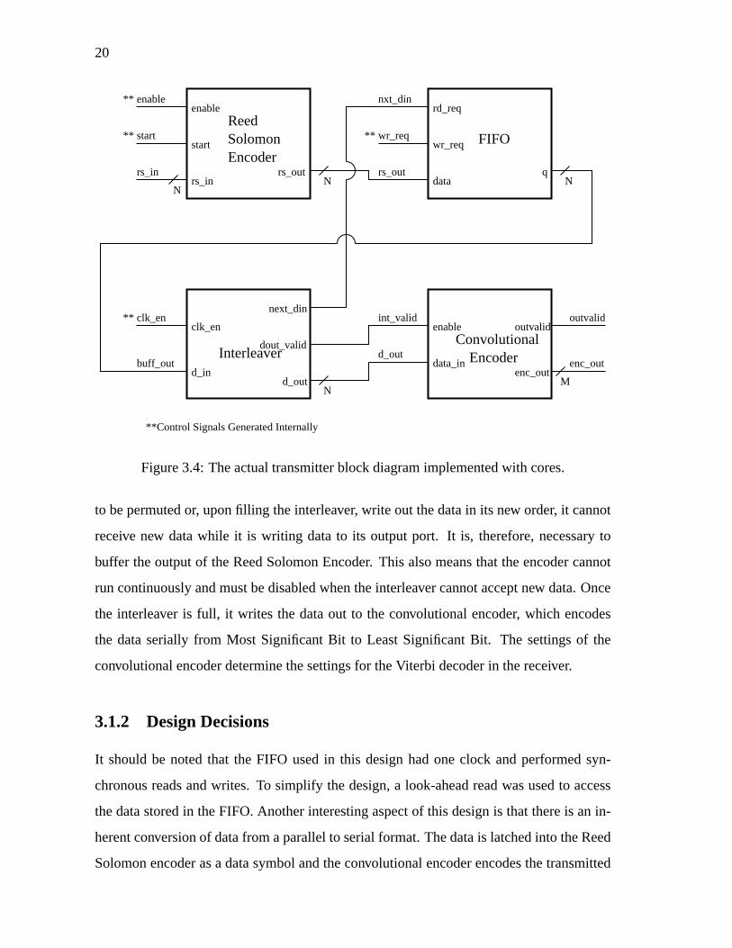
Figure3.4: Theactualtransmitterblockdiagramimplementedwith cores.
to bepermutedor, uponfilling theinterleaver, write out thedatain its new order, it cannot
receive new datawhile it is writing datato its outputport. It is, therefore,necessaryto
buffer theoutputof theReedSolomonEncoder. This alsomeansthat theencodercannot
run continuouslyandmustbedisabledwhentheinterleavercannotacceptnew data.Once
the interleaver is full, it writes the dataout to the convolutional encoder, which encodes
the dataserially from Most SignificantBit to LeastSignificantBit. The settingsof the
convolutionalencoderdeterminethesettingsfor theViterbi decoderin thereceiver.
3.1.2 DesignDecisions
It shouldbe notedthat the FIFO usedin this designhadoneclock andperformedsyn-
chronousreadsandwrites. To simplify thedesign,a look-aheadreadwasusedto access
thedatastoredin theFIFO.Anotherinterestingaspectof this designis thatthereis anin-
herentconversionof datafrom aparallelto serialformat.Thedatais latchedinto theReed
Solomonencoderasa datasymbolandtheconvolutionalencoderencodesthetransmitted

21
databit by bit. Thisrequirestwo clocks– onefor theparalleldataandanotherfor theserial
data.
Initially, the circuit was implementedwith a serial clock and the parallel clock was
derivedon-chip.This wasdoneto simplify thetestvectorsusedto verify thechip’s func-
tionality. It was not the final implementationhowever, as clock division using on-chip
logic would createtiming problems.This is becausethesecondclock, theparallelclock,
would be usingnormalsignalrouting pathsthroughthe switchesasopposedto the ded-
icatedclock signalrouting architecture.Therefore,whenthe final placeandrouteof the
circuit wasperformed,theparallelclock signalwasimplementedasacircuit input.
As discussedat thebeginningof thechapter, aconvolutionalencodercorewascreated
alongwith a customdesignimplementation.Thesetwo moduleswere interfacedto the
transmittercircuit by separatecomponentdeclarationsthat wereselectively instantiated.
Also, the interleaver allows usersto selectoneof two methodsfor permutingdata-either
in blocksor convolutionally. It wasdecidedthat for thepurposeof this study, thesimpler
circuit, theblockencoder, wouldbeused.
Finally, theencodeddataproducedby theconvolutionalencoderwasleft unpunctured.
For thepurposeof this study, transmissionsizeis unimportant,asis increasingor decreas-
ing theoverall Bit Error Rate(BER) achievedby thereceiver circuit. This is becausethe
focusis on thedesignexperience,asopposedto designingthebestpossiblefinal system.
3.2 Convolutional EncoderCore
The focusof this thesisis to determinehow usingcoresaffectsthe designmethodology
usedfor SoCs.Oneunderlyingconceptthatmustbeaddressedby thecoredesignindustry
is what the actualdefinition of a core is. While the differencebetweenHDL modules
andhardcoresis obvious, the differencebetweena soft coreandan HDL moduleis a
moreobscurearea. It is the responsibilityof the coreindustryto provide guidelinesand
standardsto differentiatebetweenacoreandnormalHDL code.TheVSIA is dedicatedto
establishingstandardsto beusedin thedesignindustry[5].
A soft coreshouldbedesignedwith testbenchesthattheusermayutilize to verify the

22
functionalityto guaranteethat it meetstheir specifications.Soft coredesignsaremodules
of codethat arereusablein differentapplications.They have no fixed placement,which
meansthat therecanbe no performanceguarantees,but they provide a greaterdegreeof
flexibility . The designsmayoftenbe parameterizable,which enablesthecoreto beused
in a largernumberof applicationsby providing a greaterdegreeof freedom.Documenta-
tion describingtheoperationof themoduleis alsoessentialto enablethird partyusersto
incorporatethecoreinto theirdesigns.
3.2.1 Overview of the Core
Toobtainsomeinsightinto thepresentstateof coredesigntechnology, asoftConvolutional
EncoderCorewasdesignedusingVHDL. This coreencodesa transmittedbitstreamwith
specificconvolutional codesfor later error checkingby a Viterbi receiver so that it may
resolvepossiblebit errors.By definingtheavailableparametersin thecore,theuserselects
theminimalnumberof two generatingpolynomialsaswell astheconvolutionalcodes.The
portsto thecorearedescribedin Table3.1 andthe userdefinedvariablesareoutlinedin
Table3.2.
Figure3.5 illustratesthe functionality of the convolutional encodermodule. As can
be seenfrom the diagram,the right side of the figure containsthe actualconvolutional
encoderthatencodesthebitsto transmit.Theleft half of theconvolutionalencodermodule
containsa register, a counter, anda multiplexer. Theregisterstorestheinput symbolfrom
thedata in bus. Thecounteris usedto selecta bit of thesymbolthroughthemultiplexer.
This bit will be usedby the convolutional encoderto generatethe encodedoutput bits,
encout.
Theconstraintlengthis equalto thenumberof registerslessonein theencodingpath.
The userprovides the valuesof the generatingpolynomialsfor the circuit illustratedin
Figure3.6. The bits set in the generatingpolynomial signify the connectedtapsto the
delaypath. The mostsignificantbit is connectedto the input A andthe leastsignificant
bit is connectedto the outputB. A generatingpolynomial is requiredfor eachcodedbit.
Figure3.6displaystheencodingcircuit for anencoderwith two encodingbits,aconstraint
lengthequalto five,andgeneratingpolynomialsGA equalto 19 andGB equalto 29.

23
reset
enable
sys_clk
data_in
N
**
enc_out
M
** Control Signals Generated Internally
A
clk
enable
clk
outvalid
Counter
Register
Encoder
Multiplexer
Figure3.5: Block diagramof theconvolutionalencodermodule.
+
+
A ‘1’ ‘1’ ‘0’ ‘0’ ‘1’
‘0’= 19GA
10= 23
8
‘1’GB = 29
10= 35
8
Register(Delay)
Register Register Register(Delay) (Delay) (Delay)
Figure3.6: Block diagramof theencodingcircuit illustratingfunctionality.
24
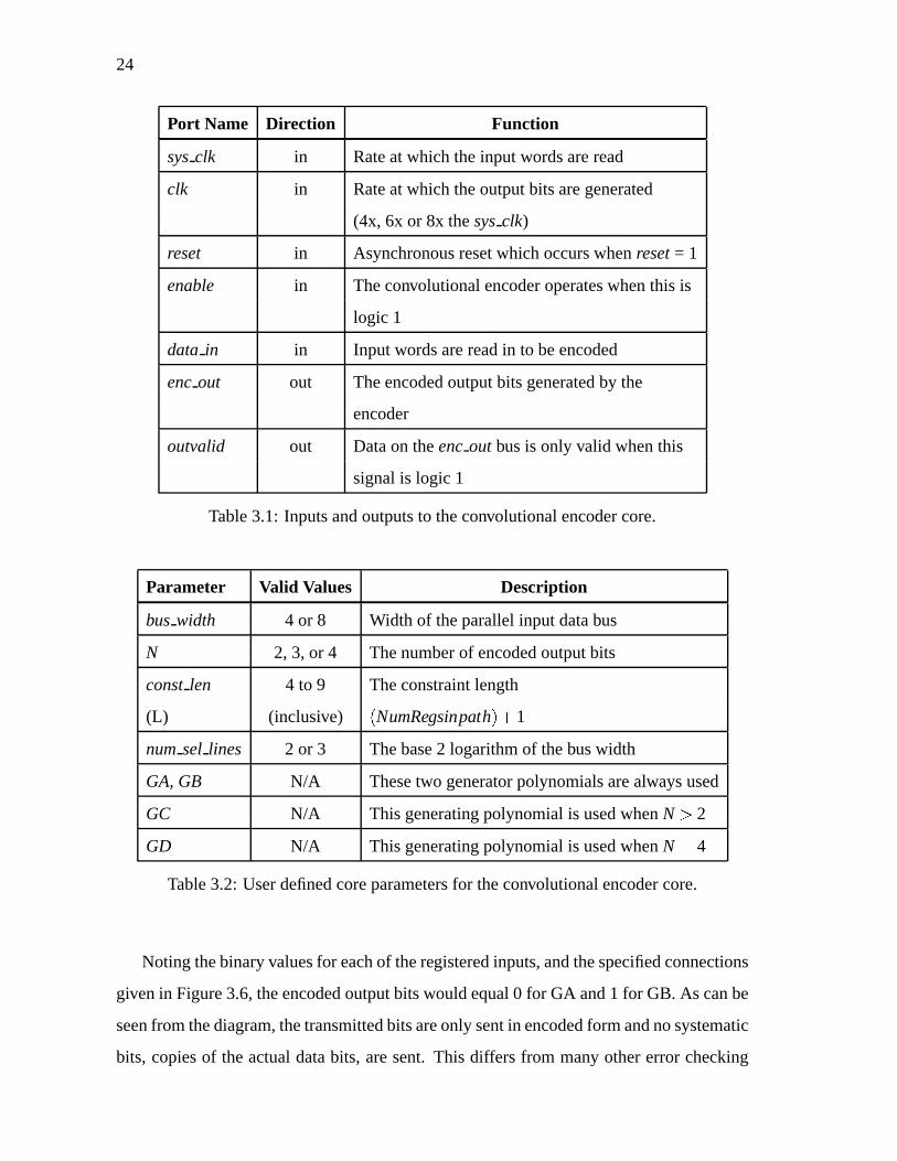
Port Name Dir ection Function
sysclk in Rateat which theinput wordsareread
clk in Rateat which theoutputbitsaregenerated
(4x, 6x or 8x thesysclk)
reset in Asynchronousresetwhich occurswhenreset= 1
enable in Theconvolutionalencoderoperateswhenthis is
logic 1
data in in Inputwordsarereadin to beencoded
encout out Theencodedoutputbits generatedby the
encoder
outvalid out Dataon theencout busis only valid whenthis
signalis logic 1
Table3.1: Inputsandoutputsto theconvolutionalencodercore.
Parameter Valid Values Description
bus width 4 or 8 Width of theparallelinput databus
N 2, 3, or 4 Thenumberof encodedoutputbits
constlen 4 to 9 Theconstraintlength
(L) (inclusive) � NumRegsinpath��� 1
num sel lines 2 or 3 Thebase2 logarithmof thebuswidth
GA,GB N/A Thesetwo generatorpolynomialsarealwaysused
GC N/A Thisgeneratingpolynomialis usedwhenN � 2
GD N/A Thisgeneratingpolynomialis usedwhenN � 4
Table3.2: Userdefinedcoreparametersfor theconvolutionalencodercore.
Notingthebinaryvaluesfor eachof theregisteredinputs,andthespecifiedconnections
givenin Figure3.6,theencodedoutputbitswouldequal0 for GA and1 for GB. As canbe
seenfrom thediagram,thetransmittedbitsareonly sentin encodedform andnosystematic
bits, copiesof theactualdatabits, aresent. This differs from many othererror checking

25
Sys_clk
Clk
Reset
Enable
Data_in
Outvalid
Enc_out
8A4
00 11 01 10 11 01 11 10
F
Figure3.7: Timing diagramof theconvolutionalencoder.
schemessuchastheReedSolomonroutinedescribedin latersections.
Finally, Figure3.7 containsa timing diagramto clarify any remainingquestionsasto
theoperationof theconvolutionalencoder. Thesystemrequirestwo clock inputsandhas
an active high resetfor all of the registersand the counterin the encodermodule. The
enablesignal is alsoactive high and is usedto turn the encoderon andoff. When the
encoderis enabled,the datasymbolsarelatchedfrom thedata in buson the rising edge
of thesysclk. Every rising edgefrom theclk signalclocksa bit from the registereddata
symbolinto thedelaypathandgeneratesanew encodedoutput.
3.2.2 DesignDecisions
Thecircuit is designedusingtwo clock signals:oneto loadthedatasymbols,andoneto
output the encodedbits serially. Two clocksareusedso that the overall circuit canrun
at fasterspeeds.If therewereonly oneclock, it would have to be artificially dividedby
the numberof input bits in the circuit. This is becauseparallelsymbolsarelatchedinto
theconvolutionalencoderandthenencodedserially. This couldsignificantlydecreasethe
throughputof the transmittercircuit becausethe limiting factorfor thespeedof both the
serialandparallelclock becomesthe encodingcircuit. If two clocksareused,then the
serial encodingof the dataoperatesindependentlyof the parallel portion of the circuit,
removing thetiming dependencies.

26
The core useris also responsiblefor settingthe numberof selectlines for the mul-
tiplexer. This is due to the difficulty of providing an equationthat could calculatethe
numberof selectlinesgiventhewidth of thedata in bus.Theproblemarisesfrom thefact
thatVHDL doesnotsupportthelogarithmiccalculationnecessaryto determinehow many
selectlinesarerequiredfor any givenwidth of thedatabus.
All thegeneratingpolynomialsweresetto amaximumwidth. TheMAX+plus II com-
piler andsynthesistools had to be usedto createthesedesignsbecausethe proprietary
coresareencryptedandonly recognizedby Altera tools. Unfortunately, theAltera com-
pilation tools do not supportall of the VHDL designconstructs.For instance,a design
cannotspecifyconstantdeclarationsin theentity declaration.This makespassingvalues
from top level of thedesignto thearchitecturelevel morecumbersome.
Therefore,Aldec’s Active-HDL, version4.1, wasusedto designandtest the convo-
lutional encodercoreasit supportsall of theVHDL languageconstructs.Whenthecore
wascompiledusingAltera tools in the transmitterdesign,thecoreheaderfile wasedited
to remove theconstantdeclarationsfrom theentity declarationandtheuserwasrequired
to specifynecessarybuswidthsin boththeentity declarationaswell asin theconstantsin
thearchitecturedefinition.
Finally, therewerealsoproblemsarisingfrom theactualsemanticsof VHDL. It does
not allow a userto remove portson a conditionalbasis. In otherwords,a bus cannotbe
removed from a designby declaringit to be of width zero. With parameterizablecores,
it would often be useful to be ableto remove a port from its core. For instance,the en-
codedoutputbits hadto be transmittedon a singlebus asopposedto separatebusesfor
eachgeneratingpolynomial.Overall, thepresentsemanticsmakescoredesignmorechal-
lengingandanupdateto thelanguagethatwould includesomeof thesefeaturesshouldbe
considered.
3.3 Receiver Cir cuit
Thesecondcircuit createdusingmultiple coreswasthereceiver circuit, which servedtwo
purposes.Primarily, it is a morecomplex circuit logically andwould not have fit on the
27
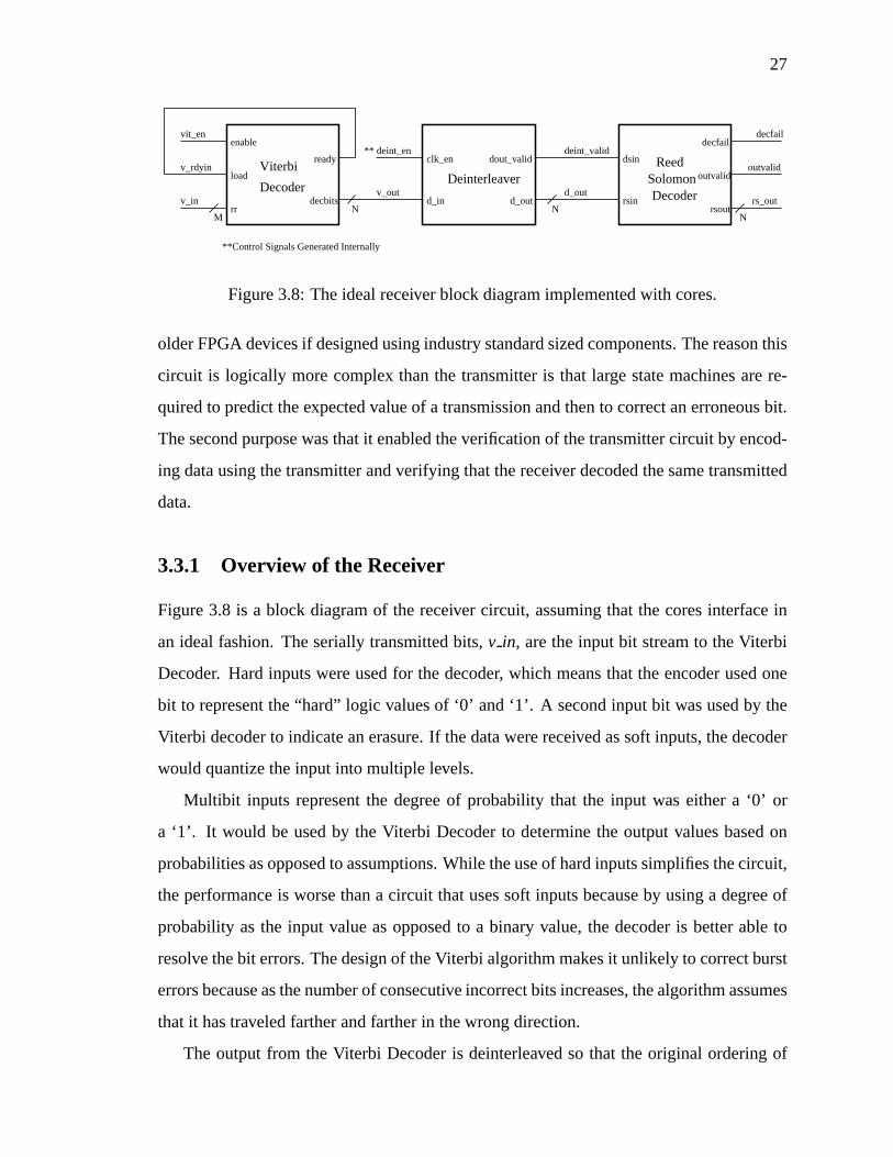
enable
d_in
dout_validclk_en
**Control Signals Generated Internally
N N
**dsin
rsin
outvalid
decfail
rr
load
deint_en
v_rdyin
vit_en
v_in
NM
deint_valid
d_outrs_out
v_out
ready
decbits d_out
decfail
outvalid
rsout
Viterbi
DecoderDeinterleaver
ReedSolomonDecoder
Figure3.8: Theidealreceiverblock diagramimplementedwith cores.
olderFPGAdevicesif designedusingindustrystandardsizedcomponents.Thereasonthis
circuit is logically morecomplex thanthe transmitteris that large statemachinesarere-
quiredto predicttheexpectedvalueof a transmissionandthento correctanerroneousbit.
Thesecondpurposewasthatit enabledtheverificationof thetransmittercircuit by encod-
ing datausingthetransmitterandverifying thatthereceiverdecodedthesametransmitted
data.
3.3.1 Overview of the Receiver
Figure3.8 is a block diagramof the receiver circuit, assumingthat the coresinterfacein
an ideal fashion.Theserially transmittedbits, v in, arethe input bit streamto theViterbi
Decoder. Hard inputswereusedfor thedecoder, which meansthat theencoderusedone
bit to representthe“hard” logic valuesof ‘0’ and‘1’. A secondinput bit wasusedby the
Viterbi decoderto indicateanerasure.If thedatawerereceivedassoft inputs,thedecoder
wouldquantizetheinput into multiple levels.
Multibit inputs representthe degreeof probability that the input waseithera ‘0’ or
a ‘1’. It would be usedby the Viterbi Decoderto determinethe outputvaluesbasedon
probabilitiesasopposedto assumptions.While theuseof hardinputssimplifiesthecircuit,
theperformanceis worsethana circuit thatusessoft inputsbecauseby usinga degreeof
probability asthe input valueasopposedto a binary value,the decoderis betterableto
resolvethebit errors.Thedesignof theViterbi algorithmmakesit unlikely to correctburst
errorsbecauseasthenumberof consecutiveincorrectbits increases,thealgorithmassumes
thatit hastraveledfartherandfartherin thewrongdirection.
The outputfrom the Viterbi Decoderis deinterleaved so that the original orderingof

28
**Control Signals Generated Internally
dsin
rsin
decfail
outvalid
rsout
decfail
q
data
enable
data
**
sel**
enable
decbits
ready
rr
loadv_rdyin
LN
.
.
.
N
d_in
dout_validclk_en** deint_en
rd_req
wr_req
data
M*N
rd_req
wr_req
data
q
rd_req1
wr_req1
**
**
M*N
reg_out
q
M*N
buff_out2
dsin
d_out
M*N
deint_out
wr_req2
**
N
N
N
v_out
vit_en
v_in
sel
v_out
buff_out1
rd_req2
rs_out
enable
q
Decoder
Viterbi
Registers(1)
Registers
FIFO A
DeinterleaverFIFO B
(M)
ReedSolomonDecoder
outvalid
Figure3.9: Theactualreceiverblockdiagramimplementedwith cores.
thesymbolsin thecodeword couldberegained.ThentheReedSolomonDecoderis used
to correctany bursterrorsthathadoccurredduringtransmission.Recallingthat theReed
SolomonDecoderdoesnot differentiatebetweena single incorrectbit in a symbol and
multiple incorrectbitspersymbol,thealgorithmis thenableto correctasymbolregardless
of the numberof incorrectbits, subjectto the numberof symbolsthat canbe corrected
per codeword. The decoderindicatesthe numberof errorscorrectedin a codeword via
thenumerrsignalor if it fails to decodethecodeword becausetherearetoo many errors,
the decfail signalgoeshigh. The output from the ReedSolomonDecoderis the initial
codeword createdby theencodercircuit. Both thedataandchecksymbolsremainandthe
designermust implementextra logic to strip off the checksymbolsfrom the codeword.
This circuit requiredextra logic to beimplementedfor interfacingpurposes;Figure3.9 is
asimplifiedversionof theactualblockdiagramof thecircuit.
TheViterbi coreis codedto haveaspecificconstraintlength.To ensurethatthedecoder
is ableto determinewhattheconvolutionally encodedbits were,thetracebackdepthmust
be setto at leastfive timesthe constraintlength[49]. Sincethe Viterbi decoderoutputs
oneor two bits at a time, the tracebacklengthshouldbe an even number. If not, when
the designertrys to restorethe serialtransmissionto its initial parallelformat, it is more

29
difficult to realignthebits. Thenumberof outputbits from theViterbi decoderis equalto
ceil � v� 2L � 1��� , wherev is thetracebackdepthandL is theconstraintlength.
The outputbit(s) from the Viterbi decoderarethenstoredin a registerto reconstruct
thesymbolsfrom theserialtransmission.Onceall thebitsof asymbolhavebeendecoded,
thesymbolis storedin FIFO A asshown in Figure3.9. Thesesymbolsarereadinto the
deinterleaverwhenit is ableto receivedata.Whenthedeinterleaver is full, thevalid output
is readinto FIFO B. Valuesarereadfrom FIFO B into theReedSolomonDecoderwhen
it is readyto decodethe next codeword. The Receiver output is the decodedcodewords
from theReedSolomonDecoder. Thesecodewordsstill includeboth thecheckanddata
symbolsandshould,thereforebethesameastheoutputfrom theReedSolomonencoder.
3.3.2 DesignDecisions
Thetransmittedbits wereassumedto behardinputs.This wasbecauseeventhoughthere
is signaldegradationover a noisychannel,it wasnot addressed,asdealingwith transmis-
sion lossesarebeyondthescopeof this study. Furthermore,no erasureswereintroduced
becausethesizeof the transmissionwasirrelevant. Instead,this researchwasmorecon-
cernedwith theactualsizeof the receiving circuit. Again, theFIFOsusedin this design
had one clock and performedsynchronousreadsand writes. To simplify the design,a
look-aheadreadwasusedto accessthe datastoredin the FIFOs. This circuit requireda
significantamountof bufferingbetweencores,whichvisibly increasedtheamountof glue
logic. This wasdoneto try andpipelinethecircuit to increasethedatathroughputof the
circuit. It wassignificantlyslowerdueto thedecodingspeedof theViterbi decoder, which
requireda large amountof time to decodethe bits. Comparatively, the time requiredby
thedeinterleaver wasnegligible andeventheReedSolomonDecodertime wasrelatively
insignificant.
Thetransmitter-receiver systemwasimplementedassumingReedSolomondatasym-
bol sizesof 4, 6, and8 bits. Althoughit wouldhavebeenpreferableto implementsystems
thatusedsymbolswith widthsall equalto powersof two, theReedSolomoncircuit would
betoo largefor 16-bitdatasymbolwidthsandtwo-bit datasymbolsarenotusefulto trans-
mit. This is why a six-bit datasymbol sizewas chosenas the third option. The Reed

30
SolomonCircuit wasalsoavailablein threedifferentformats–discrete,streamingandcon-
tinuous. Thestreamingformatwaschosenbecauseit allowedfor somepipelining of the
circuit, whereasthe discretecircuit would have causeda bottleneckin the circuit. The
continuousdecoderwasnot useddueto its size,which would have requiredthatonly the
largestdevicesof thenewestpartscouldbeused.
3.4 Summary of DesignExperience
The third party IP coresusedin thesecircuits reducedthe the total numberof gatesthat
were left to be designed.Unfortunately, much of the benefitof the coreswas lost due
to incompletedocumentation.The time saved by not designingthe coresin-housewas
partially lost in trying to determinetheiractualfunctionality. In fact,learningtheoperation
of the interleaver anddeinterleaver mayhave beenmoretime consumingthenif they had
beencreatedaspartof this research.
Over75%of thedesigntimewasspenttrying to understandhow thecoresfunctioned.
Althoughit is reasonableto expectthatbecomingfamiliar with thecoresshouldbea sig-
nificantportionof thedesign,muchof this timewaswastedondeterminingtheimportance
of undescribedinput pins, comprehendingunexplainedoutputformats,andguessingthe
throughputtimeof thecore.Thismeantthatsomeof theabstractionthatshouldhavebeen
providedby thecorewaslost. Themainbenefitof usingthecoreswasthata scaled-down
versionof eachof thecircuitscouldbecreateby changingthecoreparameters.This sim-
plercircuit couldbeverifiedfirst andonceit provedoperational,it wasrelatively simpleto
scaleup thecircuitsto createthelargersystemcircuits.
The designof the in-housecoreprovided the opportunityto view IP coresfrom the
designer’spointof view. Thereweretwo mainchallenges– languagerestrictionandusing
theavailabletoolsfor coredesignandplacement.Theproblemwith VHDL asa language
usedfor coredesignis that it doesnot offer the flexibility necessaryto fully abstractthe
core.Theotherproblemwasthatwhile theActive-HDL tool from Aldec provideda good
environmentfor designingthecore,the fact thatMAX+plus II doesnot fully supportthe
languagewhichmeansthattheinitial designhadto bechanged.
Chapter 4
Testsand Observations
This chapterdescribesthe metricsthat weredesignedto addressthe different issuesin-
volved in usingcoresin systemdesign. The proceduresusedto design,verify, andtest
thecircuits for theseattributesareoutlinedin Section4.1. Themetricshave beendivided
into two sections,thequantitativetestsandthequalitativecharacteristics.Thequantitative
testsareoutlinedin Section4.2andtheresultsaredescribedin Chapter5. Thequalitative
issuesof usingcoresin systemsdesignarediscussedin Section4.3,addressingconcerns
andproblemsthatarefacedby bothcoredesignersandcoreusers.
4.1 Experimental Procedure
Thedesignprocedurecanbebrokendown into threebasicportions. Thefirst concernwas
obtainingcoresfor thedesignof differentsystems.Thenext wasthetestingof eachcore
and the overall system. Finally, the issueof choosingtool settingsis addressedasthey
will affect theplaceandroutealgorithm,andthereforethenumericalresultsobtainedand
describedin Chapter5.
The first problemwas obtainingthird party cores. Initially, it had beenhopedthat
corescould be obtainedfrom both Altera andXilinx to build multiple systemson both
platforms. This would allow a comparisonof systemsimplementationusingIP coreson
bothof themajor industrialarchitectures.Unfortunately, the limited availability of cores
that couldbeusedto createsystemshasresultedin only onesystem.Theseconddesign
31

32
restrictioncreatedby usingcoresin thecircuit designswasthatall of theresearchhadto be
performedonapersonalcomputerrunningaMicrosoft Windowsoperatingsystem,in this
caseWindows NT version4.1. This platform wasnecessarybecauseAltera did provide
mostof their coresin a format thatwascompatiblewith theUnix versionsof MAX+plus
II.
Furthermore,it wasnotpossibleto obtainthenecessarycoresfrom Xilinx andits part-
nersto createanothertransmitter-receiversystem,whichresultedin only onesystembeing
built andimplementedusingAltera IP cores.While this is disappointing,it is an indica-
tion of theavailability of IP coresfor FPGAs.Thechallengeinvolvedin trying to obtain
coresfor designsfrom third party vendorsmadeit impossibleto obtainall thenecessary
IP blocksfor thesecondsystemon aXilinx platform.
The systemwascreatedandverified usingversion9.25 of MAX+plus II. Sincethe
Altera softwaredoesnot supporttheVHDL constructsfor File IO, all of theverification
wasdoneusingthe Waveform editor. This wasnot a problemwhenthe verificationwas
beingperformedat thecorelevel, but it did createmany challengesfor systemverification.
This is mainlybecauseverifying theoperationof theViterbi decoderrequiresthedecoding
of thousandsof bits,whichwouldbevery tediousto draw usingthewaveformeditor.
Onesolutionis to usevectorfiles to generateinputsto theWaveformEditor, but thein-
putsmustchangeat predictabletime intervals. Sinceinputsto bothcircuitsaredependent
onhandshakingsignalsanddonothavepredictabletiming characteristics,vectorfilescan-
not beusedto generatetheinput signals.As theAltera simulationtool wasnot providing
a simplemethodof verification,Aldec’s simulationtool Active-HDL version4.1, which
doessupportfile IO, waspurchasedto simplify the verificationprocess.Unfortunately,
eventhoughthecompany claimsto supportAlteradesigns,thetool doesnotsupportall of
Altera’s Megacores,which meantthatthetool couldnot beusedto verify thereceivercir-
cuit. In theend,MAX+plus II hadto beusedto verify thebasicoperationof thesystems,
dueto thelackof toolsavailablefor testingsystemswith cores.
Oncethesystemhadbeenverifiedto operatecorrectly, thetestsdescribedin Section4.2
wereperformed.The toolsweresetto optimizethe placeandroutealgorithmfor speed.
For thesmallercircuitsMAX+plus II, version9.25,wasusedto placeandroutethecircuits

33
on the FLEX 10KA devices. The larger circuits had to be placedandroutedon APEX
devices,which requiredthatQuartussoftwarebeused.TheQuartussoftwareusedfor this
researchwasversion2000.5which doesnot fully supportcorebaseddesign.Thecircuit
canbeplacedon anAPEX 20K devicebut thetiming analysisfails.
TheFLEX 10KA deviceswereusedbecausethey offeredhigh-speedperformanceand
wouldfit themajorityof thecircuits.For thelargerreceivercircuits,theAPEX 20K device
waschosenbecauseit hada largernumberof programmableresources.Whencomparing
resourceusageon thesetwo typesof devices,it is importantto qualify theterminologyas
MAX+plus II reportsthe numberof Logic Cells (LCs) andMemory bits usedto placea
circuit while Quartusstatesthe numberof Logic Elements(LEs) andEmbeddedSystem
Block bits (ESBbits)usedin thecircuit placement.
The datasheetsfor theFLEX 10K devicesreveal thata Logic Cell is simply another
termfor anLogic Elementandthey areequalunitsof measurement.Similarly, ESBbits
are comparableto the Memory bits. The final unit of the Altera FPGA architectureto
be discussedis the Logic Array Block (LAB). It is a combinationof LEs andprovidesa
slightly higherlevel of architecturalabstraction.It is importantto notethatFlex 10K LABs
arecomposedof 8 LEs while APEX 20K deviceshave 10 LEs in their LABs. Sincethere
is a fasterinterconnectrunninginternal to the LAB, changingthe numberof LEs in the
LAB couldeffect thetiming of thecircuit afterit hasbeenfitted to adevice.
4.2 Tests
The following sectiondescribesthe metricsusedto measurethe quantitative valuesof a
coreanda designthatusescores.In chip design,areausageandthemaximumclock rate
of a designareimportantmarkersof thequality of thedesign.Obviously, this is alsotrue
for designsthatusecoresbut modifiability is alsoimportantto increasethereusabilityof
thecore.Thesetestshavebeenchosento reflectthecharacteristicsthatareimportantto all
chipdesignsaswell ascharacteristicsthatareuniquelyidentifiablewith cores.

34
4.2.1 CoreParameterization
Many coreshave modifiablevaluesthatallow theuserto scalethecoreor selectdifferent
functionalitiesof interest. This can encouragegreaterreusabilityfor coressuchas the
ReedSolomonand Viterbi Decodersas they can be usedin different applications. To
test this characteristicof a core,multiple versionsof eachcore were createdto seethe
effect eachcoreparameterhason the numberof logic blocksandmemorybits required
for theplacementof thecore. If a coreis well designed,it shouldscaleits resourceusage
proportionatelyto theincreaseof thecalculationsizeor functionality.
The numberof logic blocksandmemorybits requiredfor the convolutional encoder
corecircuit werecomparedwith thoserequiredto implementcustom-designedversionsof
theconvolutionalencoder. If thecoreis describedin anefficient manner, thecoreandthe
customdesignshoulduseapproximatelythesameamountof resources.Qualitatively, the
facility of adjustingcoreparameterswasalsonoted.
4.2.2 CorePacking
As previously described,coresshouldideally be able to interfacewith little or no glue
code.Similarly, codedesignedto includecoresshouldnot requiremuchextra codeto fa-
cilitate the interfacebetweenan externally designedcoreandthe restof thedesign.The
systemsweredesignedto minimizethecodeneededto interfacethecores.Thetotal num-
ber of Logic Cells andMemory bits requiredto implementthe coresin the circuit were
determinedandcomparedto the total numberof Logic Cells andMemory bits required
to implementthe whole circuit. The goal was to determinethe percentageof resources
utilized to implementthe coresversusthe percentagewastedon connectingthe different
cores.Obviously, thegoal is to createdesignsthat limit theresourcesusedto connectthe
coressothatmoreresourcesareavailableto theessentialfunctionalmodules.
4.2.3 PredictableTiming
It is importantthat thesecircuits achieve consistenttiming characteristicsso that perfor-
manceis predictable.Multiple placeandrouteswereperformedon eachcircuit. Further-

35
more,anattemptto optimizethespeedof eachcircuit wasdoneby usingthetiming-driven
routingoption.Althoughthismightnotachievethemaximumspeedthatcouldbeobtained
by manuallyadjustingthefloorplanaftertheplaceandroute,theobjectiveof this studyis
not to studythe toolsbut to observe how the tools treatthecores. Ideally, themaximum
clockspeedof thecircuit shouldbeapproximatelyinverselyproportionalto thesizeof the
circuit.
4.2.4 Ar eaUsage
A corewith a specificsetof parametersshouldrequirethe sameamountof memoryand
logic resourcesindependentof the overall systemdesignand FPGA size, therefore,its
performanceshouldnotdegradewhenthecircuit usingthecoreis implementedona larger
device. Thetoolsshouldbesmartenoughto placethecircuit so that themaximumspeed
of thecircuit remainsrelatively constantor evenimprovesdueto theincreasedavailability
of resources.By examiningthemaximumclock frequency for a circuit andthefloorplan
obtainedby theplaceandroutealgorithm,it shouldbeevident if thecoresaretreatedas
modulesof circuitry implementedseparatelyin their own space.
4.3 Observations
Thefollowing describescharacteristicsof coredesignthatarenotquantifiableby themet-
rics of the previous section. They areequally importantwhenchoosingto implementa
corein anSoCdesignor to createacoreasthey candrasticallyaffect thedesigntimeand,
therefore,thetime-to-marketof a product.
4.3.1 Implementation Language
Therearenumerouslanguagesusedto createHardwareDesignssuchasVHDL [50], Ver-
ilog [51], AHDL [52], andC++. Of thesefour, VHDL andVerilog arethemostpopular
in industry today, with Verilog morecommonto North AmericaandVHDL moreso in
Europe.Althoughsomebelieve thatAHDL is a languagebettersuitedto IP coredevelop-

36
ment,the fact thatAHDL is not an industrystandardmeansthat it doesnot have aslarge
anappeal.This hasresultedin evenAltera’s IP designgroupmakingtheir coresavailable
for us in VHDL andVerilog designsaswell. Sincetheir coresareprovidedasencrypted
netlists,theactualdesignlanguageis unimportant,but whentheMegaWizardaskstheuser
to choosea designlanguage,aheaderfile is generatedfor thecorein thatlanguage.Other
third party IP vendorswho do provide sourcecodewill oftendesignin onelanguagebut
will willingly translatethecodeto theotherlanguagefor thecustomer.
It seemsthatneitherVHDL nor Verilog hasbecomethecommercialstandardfor core
design.CompaniessuchastheVCX do not make any requirementsasto which language
shouldbeusedby coredesignerswho make coresavailableon their webpage.They have
alsofailed to noticeany particularpatternemerging asto coredesignbeingeithermainly
in Verilog or VHDL. This is probablydueto the fact that IP is a relatively new market.
To expandtheir market, the vendorsmay createa core in one language,offer it in both
languages,andthendesignit in theotherlanguagewhenrequired.Anotherpossibility is
that the core is designedin one language,and immediatelytranslatedto the otherupon
designcompletion. The usageof C++ asan HDL is relatively new andhasnot gained
acceptanceasanindustrystandarddesignlanguage.It is believedthat therearecurrently
nocommerciallyavailableC++ IP coresat this time. ShouldC++gainawideracceptance,
it is likely thatIP vendorswill alsocreatecoresfor C++.
Still, it may be worthwhile to considerthe developmentof a new HDL which would
bebettersuitedto coredesign.This researchhasdiscoveredthatVHDL is not well suited
to coredesignin its presentform. It doesnot supportthe removal of portsfrom a design
by defininga bus width of zero. It alsodoesnot provide the ability to calculatedifficult
equations. This suggeststhat either VHDL shouldbe updatedwith new constructs,as
Verilog is to createVerilog-2000[53], or thatanotherHDL shouldbecreated.
4.3.2 Ar chitecture Independence
NumerousFPGAarchitecturesarepresentlyavailable. Thecompatibilityof coresamong
differentdevicefamiliesis specifiedby thecoreprovider. Oftentheonly limiting factorfor
backwardscompatibilityof a coreon a device is thesize.Therefore,if a coreis usableon
37
a FLEX device, it shouldbeeasilyplacedon anAPEX device,which is alsofrom Altera.
Although it shouldbepossibleto usethecoresfrom thesecircuitson APEX devices,the
difficulty of achieving afunctionalplaceandroutewith version2000.5of theQuartustools
madethis difficult to verify.
Thepossibilityof usingAlteracoresonXilinx partsor Xilinx coresonAlterapartswas
examined.Thiswasdeterminedto beimpossibledueto theformatof thecoreprovidedto
theuser. Altera’scoresarelicensedsothatthey will only compileusingsoftwareprovided
by Altera and, therefore,cannotbe usedon Xilinx parts. Xilinx coresare suppliedas
netliststhatarestructuredfor theXilinx FPGAarchitecture.Sincethesearesignificantly
different,Xilinx coresareunusableonAlteraparts.
Finally, somethird party IP vendorssuchasIntegratedSilicon Systems(ISS),sell IP
coresto both ASIC andFPGA designers.SinceISS suppliesits coresin a firm format
asa targetednetlist, thecoresarenot directly transferrablebetweenthetwo technologies.
A moreinterestingobservation is that ISS coresareavailablefor both Xilinx andAltera
FPGAdesigners.Although,theirdeliverableis afirm core,they havechosento maketheir
IP availablefor multiple typesof silicon technologies.
4.3.3 Security
IP vendorshave theoptionof providing thesourcecodeor anencryptednetlist for a core.
Obviously, thesetwo methodshave different security issues. If a vendorprovides the
sourcecodeto theuser, themainsecurityissueis to ensurethatthecoreis only usedby that
company underthespecifiedtermsof theagreementbetweenboth parties;misuseof the
corewould likely leadto a lawsuit. Both partiesmustbetrustedto respecttheagreement
and,if therearequestionsof enforceability, thenpossiblerisksshouldevaluated.
If avendoronly providesanencryptednetlistof thecore,theissueof maintainingcore
securityis alsoa factor. Theencryptionmethodologyshouldberobustenoughto prevent
anindividual from reconstructingthesourcecode.Ideally, no oneshouldbeableto break
the encryption,but realistically, as long asthe costof breakingthe encryptionis greater
thanthatof redevelopingtheactualcore,theencryptionis reasonablysecure.Companies,
suchasAltera,encrypttheir sourcecodeandtheirusersmustthenobtaina licenseto fully

38
utilize thecore.
Fromtheusersviewpoint, encryptionof a corecanmake thedesignprocessvery dif-
ficult. Thefirst problemis that theencryptionnormally interfereswith theusageof tools
from othervendors.By limiting thetools thatcanbeusedin thedesignprocess,thecore
maypreventthecompleteverificationof thedesign.Furthermore,theuseris unableto edit
thecodewhich meansthat theremaybecertainchangesthatwould significantlyimprove
theoveralldesignbut they cannotbeimplemented.Finally, theinability to accessthecode
providesfurtherfrustrationwhenthecoreis accompaniedby poordocumentation.Without
thesourcecodeandgooddocumentation,thecoreis ablackboxwith unknown behavior.
4.3.4 Legal Issues
It is importantto realizethattheconceptof IntellectualPropertyassomeform of reusable
hardwaredesignis relatively unestablishedin a legalsense.Thisoftenresultsin protracted
contractualnegotiationsassomeof thelaws arenot intuitive. For instance,a vendormay
licenseacoresuchthattheownershipof theintellectualpropertyof thecoreremainswith
thevendor(licensor). If a coreweresold, insteadof licensed,thenit couldnot besubse-
quently licensedfor useby any othercompany becauseit would belongto the company
who hadpurchasedit. A licensingcontractualarrangementleadsto the situationwhere
any modificationsto acorearethepropertyof thelicenserandnot thedesigner.
The licensewill often also limit the useof the core,andany derivation thereof,to a
specificpurposeonspecifiedsilicon. Therefore,while thesystemdesignis theintellectual
propertyof the designer, the core and any modificationsmadeto it are the intellectual
propertyof thecorevendor. This problemdid not exist whenIP wasimplementedin the
form of chipsbecausea chip is fixedandunchangeable.An individual couldnot change
the implementation,algorithm or the performanceof the IP as it had beenburnedinto
the silicon. Although soft coresoffer the benefitsof flexibility , they also presentnew
challengesin IP protection.

39
4.3.5 Modular CoreDesign
Whenthe convolutional encodercorewasdesigned,the designwasmadeasmodularas
possible. By doing this, it was hopedthat unusedsectionsof codecould be removed
so that unnecessaryresourceswould not be wasted.This wasaccomplishedby usingIF
GENERATE statementsso that this extra codecould be addedto the basicdesignwhen
necessary. Unfortunately, VHDL forcestheadditionof unnecessarycodesometimesdue
to its syntax.Thelanguagewill notallow theremoval of ports,whichcanbecumbersome
whenacoreis scalableasis theconvolutionalencodercore.
Theotherproblemarisesfrom inheritanceandthepassingof parametersfrom onelevel
of thedesignto another. It is not possibleto assigna variablebussizeat theupmostlevel
of the design.This obviously causesproblemswhenthe input or outputbusof a coreis
dependentonasizeparameter. Theusercannotsimplyentervaluesfor theconstantsin the
entitydeclarationbut mustalsochangethevaluesof thebuswidths.While having theuser
changethevaluesof thedatabusesmanuallysolvestheproblemat abasiclevel, it creates
anotherproblem.Theabstractionthat thedesignerwishesto achieve by usingcoresis no
longerintact.
4.3.6 CoreAmalgamation Effects
Oftena largeamountof gluecodeis requiredbetweencoresevenwhenthey arefrom the
samevendor. This shouldnot benecessaryif thecoredesignerplanswell enoughahead.
Realistically, someof thecoresin thesedesignsdonotfit togetherwell – eventhoughthey
areoftenusedtogether– sothat they requirenumerousregistersandbuffers. Also, anef-
ficient placementof coredesignsnormallyrequiresthat thecompilerintelligently remove
redundantcodesuchassignalstied high or low permanently, registerspermanentlyen-
abled,etc..While thetoolsavailabletodaynormallyperformthis function,mostdesigners
would prefer that the removal of thesedevicesoccurredat a sourcelevel asopposedto
curingtheoptimizationof thecircuit sothatthereis nopossibilityof failure.

40
4.3.7 Methodsof Obtaining Cores
Whencoresarenot parameterizable,asin thecaseof a PCI core,thesimplestmethodfor
auserwouldbetheability to go to anonlinelibrary/catalogueandfill outa requestfor the
core.Upondoingso,theusercouldbeemailedthecoreor allowedto proceedto a secure
part of the vendor’s network to download the core. Therearevery few concernsabout
beingableto obtainanotherversionof a corein this casebecausethereareno variables
which meansthereis only onecore. Thecoreis designedto operateasis andin no other
fashion.
In thecaseof parameterizedcores,it is preferablethat the requestbe for theuseof a
coregenerator, suchasaFinite ImpulseResponse(FIR) filter generator. Theuserwantsto
beableto changetheparametersettingswithout having to requestyet anothercore. This
freedomenablestheuserto easilyfine tunea corefor thedesignin which it will beused.
It mayalsoallow theuserto learntheoperationof thecoreonascaleddown versionof the
final core,simplifying thelearningprocess.
4.3.8 Toolsfor IP Cores
Thetoolsthatwereavailablefor testingthesecircuitsusingIP coreswereinsufficient. To
provide for thoroughverificationof acircuit’s functionality, it is crucialthatinputfilescan
beusedto generatethe input signalsandoutputfiles canbeusedto storetheresults.As
previously mentioned,this wasnot possiblefor this system.Thedesignof thecoreusing
Aldec’s Active-HDL wassuccessfulandallowedtheuserto createa thoroughtestbench.
Unfortunately, when this core was incorporatedinto the rest of the design,it had to be
changedbecauseMAX+plus II doesnot supportconstantdeclarationsin theentity decla-
ration which is an essentialcomponentof user-designedIP cores. This meansthat they
cannotsimplybeinstantiatedandimplementedin asystemdesign.
Finally, Altera’s new Quartussoftware,version2000.5,did not provide adequatesup-
port for theirown coresincludedin auser’sdesign.As canbeseenfrom thissummary, the
toolsavailabledo not provide adequatesupportfor theIP coredesignprocess.To protect
their IP, Altera hasmadeit so that their IP canonly be usedwith their tools. Sincetheir

41
designandsynthesistools arenot the bestonesavailable,beingrestrictedto their usage
couldaffect thequality of thefinal design.
4.3.9 Inf ormation Abstraction
When a designerchoosesto usea core, as opposedto personallycreatingthe module,
the time-to-market shouldbe shortenedby the abstractionof the detail of that core. The
designerwouldpreferto treatthecoreasablock,consideringonly theinputsandoutputs.
The following sectionsdescribehow the tools anddocumentationprovided by the core
vendorhelpto abstractthis informationfor thedesigner. If thetools,andmoreimportantly
thedocumentation,arewell specified,thisgreatlyfacilitatesthejob of thedesigner.
4.3.9.1 CoreGenerationTools
Theobjectiveof usingcoresin SoCdesignsis to providea level of informationabstraction
soasto simplify theuseof thecore. By looking at differentcoregenerationtools, it was
seenthattheGraphicalUserInterfaces(GUIs) availablefor Altera’s ReedSolomonCom-
piler andDeinterleaverprovidedausefullevel of abstraction.GUIswerealsoavailablefor
othercoressuchasFIFOsandregisterLPMs but thesewerenot necessaryasthey did not
abstractverymuchinformation.
The Viterbi corehada higher level AHDL file into which the userenteredthe input
parameters.Although thereis lessabstractionto this design,a knowledgeof AHDL was
not requiredto determinehow to enterthenew parameters.Themajorbenefitof theGUIs
available,suchasaMegaWizard,is thatthey abstractthelanguageof thecoreitself sothat
it maybegeneratedin AHDL, VHDL, or Verilog. Thewizardalso“remembers”thestate
andconfigurationof thecore,simplifying thechangingof acorein adesign.
4.3.9.2 Documentation
Thedocumentationprovidedby thecorevendorfor thedesignersshouldbesimilar to that
of a manualfor anIC. It shouldgivea succinctdescriptionof thecoreasa blackbox,de-
scribingall theexternally-seenstatesof thecore.It shouldalsoabstracttheinnerworkings

42
of the coreso that unnecessarydetailsremainhiddenwhile it is easyto amalgamatethe
coreinto afinal design.
Thedocumentationfor thecoresreadfor this thesiswerepoorin general.Overall, the
documentationdid not enablea designerto understandhow to usethe corequickly. In
fact, it is estimatedthat the majority of designproblemsarosedueto unclear, incorrect,
or absentdocumentation.Theindustryattitudetowarddocumentationappearsto bethatit
is of secondaryimportanceandthataslong asthecoreis readyandtechnicallycorrect,a
corereleasecanoccur.
Unfortunately, without clearandsuccinctdocumentation,theactualcoremaybewell
implemented,but thedesigneris sorelytestedto determinehow to useit. This shouldbe
consideredasa seriouscomplaint– usingIP coresin SoCdesignsis only beneficialwhen
the time andcost incurredto usethemis lessthanwhat is requiredto generatethe core
designin-house. Poordocumentationis not only detrimentalto the designerbut to the
vendoraswell. If thedesigneris unableto resolvetheirquestionsfrom thedocumentation,
they will requirecustomersupport.Thelargertheamountof customersupportrequiredto
usea core,the lessnet profit will result from its sale. This thesishasillustratedthat the
documentationfor somecoresis poorenoughthatthereis questionablesavingsof timeand
money.
4.4 DesignGuidelines
Having completedthedesignprocess,a setof designguidelinesweredevelopedto reflect
themethodologyusedto designeachcircuit.
1) Determinewhatcommerciallyavailablecoressuit your design.Thereis almostcer-
tainly morethanonecoreavailablefor your application.Try to ensurethatconsideration
is givento IP coresfrom multiplevendors.
2) Checkthatany corespurchasedwill beusablewith thetools in thedesignprocess.
If this is not thecase,ensurethat therearetoolsavailableon themarket thatwill support
thecore.

43
3) If a specificcoreis availablefrom morethanonecompany, investigatetheprosand
consof usingacorefrom thatcompany. Thingsto look for:
� Meetsthespecificationsfor your design
� Gooddocumentation
� Goodtechnicalsupport
� Goodtestbenchesillustratinghow thecomponentfunctions.It shouldbenotedthat
themorecomplex thecore’sbehavior, thelargerthenumberof testbenchesthatmay
benecessaryto thoroughlydescribeits behavior.
� Goodinterfacestructure
� Any other “bonus” deliverablessuppliedby the company, suchas a higher level
modelof thecoresfunctionality.
If acorefrom thiscompany hasbeenusedin apreviousdesign,whatwasyourexperience?
If it wasnot goodandthis is theonly company thatsellsthis core,considerthat it might
bemorecosteffective to have it designedin house.Remember, for coresthatarenot well
documented,it can take almostas long to determinea core’s functionality as it can to
designit. Also considerthat if the circuit mustrun at extremelyhigh speeds,coresmay
notgiveyou theperformanceyouneed,andmusttherefore,bethoroughlyinvestigated.
4) Having chosenthecoresto beusedin your design,testthemasseparateentitiesso
that thereis no “mysterious”behavior. Thedesignermustfully comprehendthebehavior
of thecomponentfor all valid inputsto usethecorein a design.
5) Determinewhatgluelogic is neededto connectthedifferentmodulesin yoursystem.
Considerthebestway to interfacethecoresuchthat theglue logic is minimizedwithout
destroying theoverall systemthroughput.

Chapter 5
Discussionof Results
Thetransmitterandreceiversystemsmaybedividedinto threemaincomponents-theReed
Solomonmodule,theInterleavermodule,andtheConvolutionalmodule.Eachcomponent
wasdesignedwith adjustableparametersthatwerepermutedin sevendifferentways.The
coreswerecombinedin uniquewaysto createninedifferentimplementationsof the two
systems.Therearethreedatasymbolbus widths usedin this studyandeachwidth has
threedifferentcoreconfigurations.Thebuswidthswerechosento befour, six, andeight
bits. Theresultswerestudiedto determinetheeffectof parameterizationandcorepacking
on resourceusageandthemaximumclock rateof thesetwo systems.
5.1 CoreCir cuit Configurations
Table5.1providesa descriptionof thedifferentReedSolomoncomponentsusedto create
the two systems. Although it was possibleto vary the root spacingin the polynomial
generatorand the first root of the polynomialgenerator, thesevalueswere left constant
at oneandzerorespectively. This is justified by the fact that thesearesuggestedin the
documentationaspossiblevaluesfor thesecomponents.Also, thesevalueswereadjusted
for thers 1 circuit andit wasdeterminedthatchangingthevalueshadlittle to no effecton
thenumberof LCsusedto implementthecircuit.
Table5.2 describesthedifferentInterleaver/Deinterleaver componentsusedin the re-
ceiverandtransmittersystems.Thesymbolwidth is equalto thenumberof bitspersymbol,
44

45
ReedSolomon Bits per Symbols CheckSymbols Field
Cir cuit Labels Symbol per Codeword per Codeword Polynomial
rs 1 4 5 4 19
rs 2 4 15 4 19
rs 3 6 15 4 67
rs 4 6 19 8 67
rs 5 6 52 8 67
rs 6 8 52 8 285
rs 7 8 204 16 285
Table5.1: Descriptionof ReedSolomoncircuits.
asindicatedin columntwo of bothTable5.1and 5.2.For thesecircuits,thesymbolwidth
the interleaver mustbeequalto thatof theReedSolomoncomponentin eachcircuit. To
ensurethatthedesignis robustagainstbursterrors,multiplecodewordsareinterleaved.
For smallercodewords,four codewordsareinterleavedwhereasfor largercodewords
only two codewordsareinterleaved.Thiswasaccomplishedby alwayssettingthenumber
of rowsto four andsettingthenumberof columnsto thenumberof symbolspercodeword,
N, for the first four circuits, andN 2 for the remainingthree. The interleaver corealso
requeststhattheuserspecifythenumberof symbolsin acodeword,thesymbolwidth, and
theestimatedbit- errorrate.Thesevaluesarejust usedto provideestimatesfor theuseras
to theeffectivenessof theinterleaving valueschosen.
TheConvolutionalEncoder/Viterbi Decodercomponentsof thereceiver andtransmit-
ter systemsareoutlinedin Table5.3. Thesystemsweredesignedsuchthatthenumberof
codedbits rangedbetweentwo andfour. The constraintlengthwasset to be eitherfive
or seven andthe tracebackdepthwassetto be five timesthe constraintlengthplus one.
The convolutional encodercoreallowed the userto specifyany valuefor the generating
polynomialin theheaderfile. Thecustom-designrequiredtheuserto edit theactuallogic
equationsusedto generatetheencodedoutputsto changethegeneratingpolynomials.Ob-
viously, bothmethodseffect thechange,but theabstractionprovidedby theconvolutional

46
Interleaver/ Deinterleaver Bits per Number Number
Cir cuit Labels Symbol of Rows of Columns
int 1 4 4 5
int 2 4 4 15
int 3 6 4 15
int 4 6 4 19
int 5 6 4 26
int 6 8 4 26
int 7 8 4 51
Table5.2: Descriptionof interleaveranddeinterleavercircuits.
encodercoreis moreuser-friendly.
Viterbi decoderis designedwith suggestedvaluesfor thegeneratingpolynomialsgiven
thenumberof codedbits,N, andtheconstraintlength,L. Thesymbolwidth mustbeequal
to thatof the interleaver. TheViterbi decoderalsoallows theuserto selectthenumberof
bits representingeachencodedbit readoff the channel.Sincevaryingvoltagelevelsare
usedto representthevariousbit levels,afiner resolutionmakesthechannelmorerobustto
noise.
5.2 SystemCir cuit Configurations
The previous tableshave describedthe differentcomponentsusedto createthe two sys-
tems. Table5.4 providesa descriptionof the basicsystemcreatedby delineatingwhich
componentswereusedfor eachinstantiation.Thesecombinationswerechosento provide
insightasto theeffect of changingthedifferentparameters.Implementation8c wascho-
sento representcomponentsthat aretypically in usetoday. The rs 7 andvit 7 modules
arecommonlyusedin Digital VideoBroadcasting(DVB). An explanationof thecompiled
dataresultsis foundin thefollowing sections.
Thenamingof thesystemfolloweda simpleconvention.If it is a transmitter, thenthe

47
Convolutional Encoder/ Number Constraint Traceback Symbol
Viterbi Decoder of Coded Length Depth Width
Cir cuit Labels (Bits (N) ) (L)
vit 1 2 5 26 4
GA=19,GB=29
vit 2 2 7 36 4
GA=91,GB=121
vit 3 3 5 26 6
GA=21,GB=27,GC=31
vit 4 3 7 36 6
GA=91,GB=101,GC=126
vit 5 4 7 36 8
GA=93,GB=93,
GC=103,GD=115
vit 6 4 5 26 8
GA=21,GB=23,
GC=27,GD=31
vit 7 2 7 36 8
GA=91,GB=121
Table5.3: Descriptionof convolutionalencoderandViterbi decodercircuits.
first two lettersof the circuit nameare“tx”, otherwisethe letters“rx” wereusedfor the
receivercircuit. Thedigit in thenamerepresentsthewidth of theinputdatabusto theReed
SolomonEncoder. Finally, the letters‘a’, ‘b’, and‘c’ wereusedto differentiatebetween
thethreecircuitsimplementedfor thatparticularbuswidth.

48
Transmitter/Receiver ReedSolomon Interleaver Convolutional
Cir cuit Labels Cir cuits Cir cuits Cir cuits
tx 4a,rx 4a rs 1 int 1 vit 1
tx 4b,rx 4b rs 2 int 2 vit 1
tx 4c, rx 4c rs 2 int 2 vit 2
tx 6a,rx 6a rs 3 int 3 vit 3
tx 6b,rx 6b rs 4 int 4 vit 4
tx 6c, rx 6c rs 5 int 5 vit 3
tx 8a,rx 8a rs 6 int 6 vit 5
tx 8b,rx 8b rs 7 int 7 vit 6
tx 8c, rx 8c rs 7 int 7 vit 7
Table5.4: Descriptionof transmitterandreceivercircuits.
5.3 Parameterization Effects
Table 5.5 provides the resultsof the placeand route of eachof the ReedSolomoncir-
cuitsdescribedin Table5.1. Theencoderrequiresno memorybits for its implementation
whereasthe decoderdoes. The numberof bits requiredis dependenton the codeword
lengthandthe numberof bits per symbol. As canbe seenfrom Table5.1 by comparing
theparametersusedfor thecorecircuits to thenumberof LCs requiredto implementthe
encodercircuit, thenumberof LCs is minimally affectedby thenumberof datasymbolsin
thecodeword. This is sensibleastheencoderis letting thedatasymbolspassthroughthe
encoderunchanged.
Thenumberof LCsusedto implementtheencoderis affected,howeverby thenumber
of bits per symbolandthe numberof checksymbols. This is alsoreasonablesincethe
encodergeneratesthe checksymbolsby using from passingthe datasymbolsthrough
the generatingpolynomial. The decoder’s usageof the chip’s logic resourcesdepends
on the total codeword lengthand the numberof bits per symbol. As the decodermust
correcterrorsin both thedataandchecksymbols,independentof thesymbolwidth, it is
thereforeunderstandablethattheentirecodeword lengthaffectsthenumberof LCsusedto

49
implementthecircuit.
ReedSolomon Decoder Encoder
Cir cuit Number of Number Number of Number
Name Memory Bits of LCs Memory Bits of LCs
rs 1 256 516 0 40
rs 2 384 533 0 45
rs 3 1152 710 0 77
rs 4 1536 1134 0 106
rs 5 2304 1164 0 106
rs 6 6144 1564 0 200
rs 7 12288 2932 0 292
Table5.5: MemoryandLC usageof ReedSolomoncircuits.
Table5.6outlinestheresourceusageof theInterleaver circuitsdescribedin Table5.2.
As can be seenfrom the resultsin Table 5.6, the deinterleaver and interleaver circuits
requirethesamenumberof LCsandmemorybits. Thisis areasonableresultasthecircuits
arealmostidentical.Theonly differenceis theorderin which thedatais loadedandread
out of thememory. It is alsointerestingto notethat thesecircuitsrequirevery little logic
resourcesbut mostlymemoryresources.Sincememorymustbeallocatedin blocks,evenif
only 1 memorybit is actuallyusedfrom theblock,therestof theblockbecomesunusable.
This meansthat that thenumbersprovidedin Table5.6 representthetotal numberof bits
in thememoryblocksusedby thecircuit asopposedto theactualnumberof bits usedby
thecircuit.
Table5.7providestheresourceusageof theconvolutionalcircuits.Neithertheencoder
northeViterbi decoderrequirememorybitsin their implementations.Theencoderrequires
minimalLCsasit is simplyaselectiveexclusive-oroperation,but theViterbi decoderuses
a significantamountof logic to implementa trellis to provide error correctionto the bit
stream.As the constraintlengthincreases,the sizeof the trellis increasesexponentially.
The Viterbi circuitry is independentof the symbolwidth but not of the numberof coded
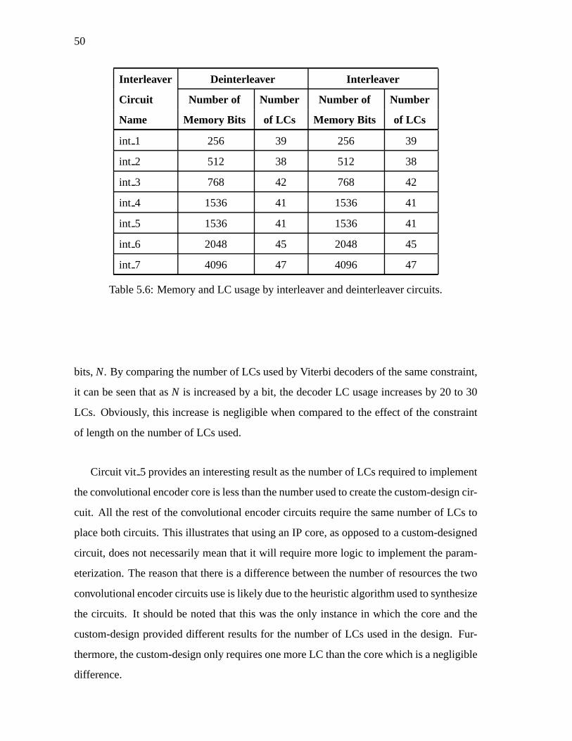
50
Interleaver Deinterleaver Interleaver
Cir cuit Number of Number Number of Number
Name Memory Bits of LCs Memory Bits of LCs
int 1 256 39 256 39
int 2 512 38 512 38
int 3 768 42 768 42
int 4 1536 41 1536 41
int 5 1536 41 1536 41
int 6 2048 45 2048 45
int 7 4096 47 4096 47
Table5.6: MemoryandLC usageby interleaveranddeinterleavercircuits.
bits,N. By comparingthenumberof LCsusedby Viterbi decodersof thesameconstraint,
it canbeseenthatasN is increasedby a bit, thedecoderLC usageincreasesby 20 to 30
LCs. Obviously, this increaseis negligible whencomparedto theeffect of theconstraint
of lengthon thenumberof LCsused.
Circuit vit 5 providesaninterestingresultasthenumberof LCsrequiredto implement
theconvolutionalencodercoreis lessthanthenumberusedto createthecustom-designcir-
cuit. All therestof theconvolutionalencodercircuitsrequirethesamenumberof LCs to
placebothcircuits.This illustratesthatusinganIP core,asopposedto acustom-designed
circuit, doesnot necessarilymeanthat it will requiremorelogic to implementtheparam-
eterization.Thereasonthatthereis a differencebetweenthenumberof resourcesthetwo
convolutionalencodercircuitsuseis likely dueto theheuristicalgorithmusedto synthesize
the circuits. It shouldbe notedthat this wasthe only instancein which the coreandthe
custom-designprovideddifferentresultsfor the numberof LCs usedin the design. Fur-
thermore,thecustom-designonly requiresonemoreLC thanthecorewhich is anegligible
difference.

51
Convolutional Convolutional Encoder Viterbi
Cir cuit Number of Number Number of Number
Name Memory Bits of LCs Memory Bits of LCs
vit 1 0 17 0 2248
vit 2 0 21 0 10991
vit 3 0 30 0 2270
vit 4 0 33 0 11012
vit 5 (1) 0 33 0 11039
vit 5 (2) 0 32 0 11039
vit 6 0 28 0 2299
vit 7 0 29 0 10991
Table5.7: Memory andLC usageof convolutionalencoderandViterbi decodercircuits.
The convolutional circuits labeledwith a (1) usea customdesignfor the convolutional
encodercircuit whereasthecircuits labeledwith a (2) usetheconvolutionalencodercore
circuit.
5.4 CorePacking Effects
Table5.8providesthememorystatisticsfor boththetransmitterandreceiver circuits. By
studyingcolumn four of the table, it can be seenthat the transmitteris more efficient
in its memoryusagethan the receiver for systemswith four andsix-bit symbolwidths.
However, thereceivercircuitsuselessmemoryasgluelogic thanthetransmitterswhenthe
symbolwidth is eightbits. Thisappearsto resultfrom thefactthatthememoryusagein the
transmitterincreasesby afractiondueto thechangeof bit width,but thereceiver’smemory
usageincreasesat by slightly greaterthan 100%when the bit width is increased.Allof
the systems,except for two of the receivers, tx 8b andtx 8c, have usedat least70% of
the memorybits for implementingthe IP coreswhich is within reasonabledesignlimits.
Unfortunately, it appearsthatasthetwo circuitsarescaledupin size,thetransmittercircuit
requiresagreaterpercentageof gluelogic to interfaceits cores.Thisdoesnotseemto hold
true for the receiver circuit, however, which remainsrelatively constantin theamountof

52
memoryrequiredto interfacetheIP coresto eachotherasthereceivercircuitsgetlarger.
Cir cuit Memory Total Memory Percentage
Name Usedby Cores Usedby Cir cuit of Memory
Usedby Cores
tx 4a 256 256 100
rx 4a 512 640 80
tx 4b 512 576 89
rx 4b 896 1216 74
tx 4c 512 576 89
rx 4c 896 1216 74
tx 6a 768 864 89
rx 6a 1920 2400 80
tx 6b 1536 1632 94
rx 6b 3072 3936 78
tx 6c 1536 1920 80
rx 6c 3840 4992 77
tx 8a 2048 2560 80
rx 8a 8192 9728 84
tx 8b 4096 6144 67
rx 8b 16384 20480 80
tx 8c 4096 6144 67
rx 8c 16384 20480 80
Table5.8: Memorystatisticsfor transmitterandreceivercircuits.
Table5.9givestheLC statisticsfor boththetransmitterandreceiver circuits. Column
four of thetableillustratesthatthereceivercircuitsachieveveryefficientcorepackingand
needminimalextra LCs for gluelogic. Unfortunately, thecorepackingfor thetransmitter
coresis notnearlyasgood.This is aproblempartiallydueto theactualtransmittersystem
design.Thereis overheadlogic requiredto ensurethatthesysteminterfacesproperlywith

53
theoutsideworld.
For instance,theReedSolomonEncoderis notequippedwith signalsto indicatewhen
new datawordsshouldbe suppliedto the encoder. This meansthat a counterhasto be
usedto keeptrack of the numberof datasymbolsreadin by the Encoderso that data
symbolswill not overwrite the checksignalsgeneratedby the core. If the corehadan
outputsignal indicatingwhenthe datasymbolshadbeenreadin, thentherewould be a
methodof indicatingwhenthetransmitterneededto encodeanew datasymbol.
5.5 Timing Results
Table5.10providestheresultsfor thereceiver circuits,includingthemaximumclock fre-
quency andthe device automaticallychosenfor the fitting of thecircuit. As canbe seen
from columnfive of the table,circuits rx 6b, rx 8a,andrx 8c cannotbe implementedon
any of theFlex partsasthey requiretoo many LCs. This is dueto thesizeof theViterbi
decoderin thesecircuitswhich hasa constraintlengthof sevenandmonopolizesmostof
thelogic resourcesona device,evenon thelargestof parts.
It appearsthat the placeandroute tool obtainsa timing analysisfor circuits that do
not evenfit on a device. This is probablydoneby assumingthat thereis anFPGAwith a
FLEX 10KA architecturebut is infinite in size.Obviously, this timing informationis only
anestimateandcannotbeassumedasthemaximumclockfrequency if thecircuit is placed
on anAPEX device which hasa slightly differentarchitecture.Thetiming dataalsoindi-
catesthatasthecircuit becomeslargerandmorecomplex, themaximumclock frequency
decreases.Although circuit rx 6c appearsto be an exceptionto this rule, the maximum
clock frequenciesaresoclosethatthedecreasein frequency is relatively negligible.
Sincetheplacementandroutingof thecircuit is performedusingaheuristicalgorithm,
this inconsistency in themaximumclock ratefor therx 6ccircuit is reasonable.Thealgo-
rithm basicallysearchesasolutionspacefor aminimumwhichrepresentsthebestpossible
fit for thecircuit. In doingso thethesearchmayobtaina local minimumandfail to find
the actualminimum on the searchspace.This could result in the algorithmobtaininga
relatively poor fit for the circuit, asopposedto thebestfit which explainswhy the clock

54
Cir cuit LCs Total LCs Percentage
Name Usedby Cores Usedby Cir cuit of LCs
Usedby Cores
tx 4a 96 145 66
rx 4a 2803 3027 93
tx 4b 100 272 37
rx 4b 2819 3179 89
tx 4c 104 276 38
rx 4c 11562 12052 96
tx 6a 149 349 43
rx 6a 3022 3437 88
tx 6b 180 391 46
rx 6b 12187 12748 96
tx 6c 177 406 44
rx 6c 3475 3916 89
tx 8a(1) 278 528 53
tx 8a(2) 277 527 53
rx 8a 12648 13283 95
tx 8b 367 645 57
rx 8b 5278 5796 91
tx 8c 368 642 58
rx 8c 13970 14622 96
Table5.9: LC statisticsfor thetransmitterandreceivercircuits.
frequency for therx 6ccircuit is betterthanexpected.
Although a placementcould be found on a Flex part for circuits rx 4a, rx 6b, rx 8a,
andrx 8c, the timing analysisfaileddueto a problemwith version5 of Quartussupport-
ing cores. The MAX+plus II software, however, was able to provide estimatesfor the
maximumclock frequency for rx 6b, rx 8a, andrx 8c even thoughthey did not fit on a

55
FLEX part.Whatis evenmoreinterestingis thatthemaximumclock frequenciesfor these
threecircuits weregreaterthanthat for the rx 4c circuit althoughthe tools estimatedthe
maximumclock frequency for thesecircuitseventhoughthey did not fit on theFlex parts.
Thiswasaccomplishedby assumingthebasicFlex architecture,giventhereweresufficient
logic resourcesto placethecircuit. As canbeseenfrom thetable,themaximumclock fre-
quency for the rx 4c circuit is significantlyslower thanfor theotherlargecircuits. In all
probabilitythis occurredbecausethecircuit fit on theEPF10k250partbut used99percent
of thelogic resources,hencethefasterroutingresourceswerealreadyused.
Thedesirewasto placeandroutethis circuit, aswell astheotherthreecircuitswhich
did not fit on the FLEX parts,on APEX devicesusingQuartussoftwareandto obtaina
timing analysis.Presentlyonly version5 is availablefor usein this researchwhich seems
ableto fit the circuits successfullyon a part but unableto performa timing analysisdue
to thecores. It is, however, still interestingto notethat the Quartussynthesizerchoseto
implementthe receiver circuits in a significantlydifferentfashionthanthe MAX+plus II
software. Much of thecircuit hasbeenimplementedin theESBbits asopposedto in the
LCs. It would be interestingto know what kind of effect this hason the overall circuit
timing.
Table 5.11 describesthe resultsfor the transmittercircuits using both the custom-
designedconvolutionalencoderandtheconvolutionalencodercore.Themaximumclock
frequency givenin columnfour is for theserialclockbecauseit determinestheoverallop-
eratingspeedof thecircuit. Thetiming resultsfor thesecircuitsarerelatively consistentfor
circuitsof a givenbit size. Neitherthecorenor thecustom-designedversionconsistently
achieve a bettermaximumclock frequency. Thesix-bit systemsrun at speedscomparable
to thatof theeight-bitsystems.
Obviously, FLEX FPGAsaredesignedto bettersupportsystemsthatoperateon data
thathaswidthsof powersof two sincethereareeightLEs in eachLAB. This is because
theesix-bit systemsareslowedby theproblemof bit boundariesnotalwaysfalling within a
Logic Array Block (LAB) whichhasa fastroutingarchitectureconnectingit. If thesix-bit
systemswerefit on to the architecturesuchthat only part of the symbolwere in a LAB
andtherestwerein anotherLAB, thesignalswouldhaveto travel alongtheslowerrouting

56
tracks,thusincreasingthepathbetweenregistereddata.
Cir cuit Number of Number Max Clock Device
Name Memory Bits of LCs Frequency
(MHz)
rx 4a 640 3027 41 EPF10K100ARC240-1
rx 4b 1216 3179 37 EPF10K100ARC240-1
rx 4c 1216 12052 28 EPF10K250AGC599-1
15488 1284 Uncalculated EP20K100TC144-1
rx 6a 2400 3437 36 EPF10K100ARC240-1
rx 6b 3936 12748 37 EPF10K-nofit
18688 1925 Uncalculated EP20K100TC144-1
rx 6c 4992 3916 39 EPF10K100ARC240-1
rx 8a 9728 13283 32 EPF10K-nofit
24064 2397 Uncalculated EP20K100TC144-1
rx 8b 20480 5916 23 EPF10K130VGC599-2
20480 5796 29 EPF10K250AGC599-1
rx 8c 20480 14622 22 EPF10K-nofit
32256 3679 Uncalculated EP20K100TC144-1
Table5.10:Overview of placeandrouteresultsfor thereceivercircuits.
5.6 Ar eaUsageResults
Table 5.12 provides a summaryof placing the samecircuit, tx 8a, on different size
FLEX10KA devices. As canbe seenfrom the maximumserialclock frequency results,
thefrequency decreasesasthepartsincreasein size.Thereasonfor this canbeseenfrom
thefloor plansin Figures5.1, 5.2,and 5.3. As thedevicesget larger, insteadof making
a circuit placementthat keepsthecircuit logic relatively close,MAX+plus II spreadsthe
logic all overchip. By increasingthelengthof thecritical pathin theselargerdevices,the
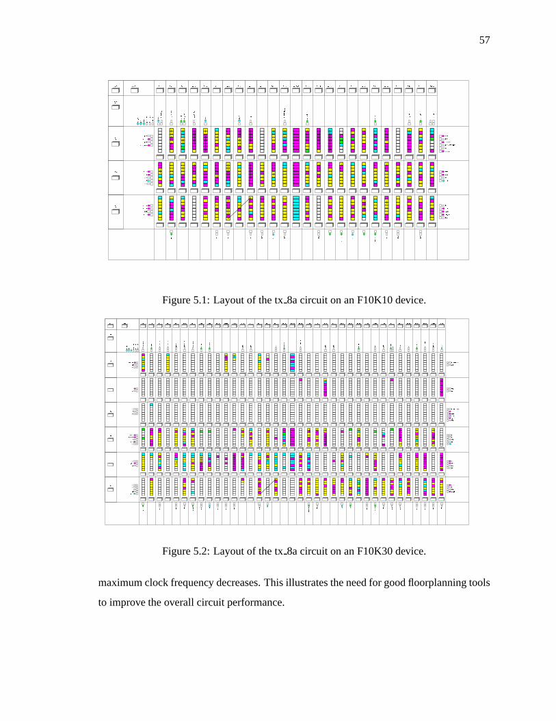
57
��� ���� ���� ������ � ! "
#$%&'
()* +,-./0 1 2 3 4
5678 9:;<=> ? @ A B
CDEFG
H I J K L
MNOPQ
R S T U V
WXYZ[ \ ]^ _
` abcdef g h i j
k l mnopq
r s t u v
w xy z{
| } ~ � �
��� �����
� � � � �
� � �����
� � � � �
�����
� ¡ ¢ £
¤¥¦ §¨©ª«¬ ® ¯ °± ² ³ ´ µ ¶
·¸¹º»
¼½¾¿ ÀÁÂà ÄÅÆÇ ÈÉÊ Ë Ì Í Î
Ï ÐÑ ÒÓ
Ô Õ Ö × Ø
ÙÚÛÜÝ
Þ ß à á â
ãäåæç
èéêëì
í î ï ð
ñ òó ôõö ÷ ø ù
úûüýþ
ÿ � � �
�����
� �
� � ��
� � � �
���� �������
! " #
$ %&'()
*+, -./01
2 3 4 5
6 789:;
<=>? @ABCDEF
G H I J
K LM NO
PQRS TUVWXYZ
[ \ ] ^
_ `abc
def ghij
klmn op qrst
u
vwxy z{ |}~�
�
��� �� �� �� ����
�
� � � � � �
� � � � �� � � � � � ¡¢ £ ¤ ¥ ¦ §¨ © ª « ¬ ® ¯ ° ± ²³ ´ µ ¶ ·¸ ¹ º » ¼ ½ ¾¿ À Á  ÃÄ Å Æ Ç È É ÊË Ì Í
Î
Ï Ð Ñ Ò ÓÔ Õ Ö × Ø
Ù Ú Û Ü ÝÞ ß à á â
ã ä å æ ç è éê ë ì í î
ï ð ñ ò ó ôõ ö ÷ ø ù úû ü ý þ ÿ �� � �
�
� � � � �� � � �
� � � � � � � � � � � � � � � ! " # $ % & ' ( )* + , - . / 0 1 2 3 4 5 6
7 8 9 : ; < = > ? @ A BC D E F G H I J K L M N
O P QR
S T UV W X
Y Z [
Figure5.1: Layoutof thetx 8acircuit on anF10K10device.
\]^_`
a bc de
f g h i j
klmno
pqrs tuv w
x y z { |
}~���
���� ���
� �
� � � � �
�����
� �����
� � � � �
¡¢£¤
¥ ¦ § ¨ ©
ª«¬®
¯°±²³
´ µ ¶ · ¸
¹º»¼½
¾ ¿ ÀÁÂÃÄ
ÅÆÇÈÉ
Ê Ë Ì Í Î
ÏÐÑÒÓ
ÔÕÖ×Ø
Ù Ú Û Ü Ý
Þ ß àáâãä
åæçèé
ê ë ì í î
ïðñòó
ô õ ö ÷ ø
ù úûüýþ
ÿ � � � �
� ����
� � � �
� �� ��
� � � � �
�����
� ! " #
$%&'(
) * + , -
./012
3 4 5 6 7
89 :;< =
>? @
A B C D E
FGHI JKLM NOPQ
R S T U VW X Y Z [ \
]^ _`ab
cd
e f g h i
jklmn
o p q r s
t uv w
x
y z { | }
~����
� � � � �
�����
� � � � �
�����
� � � � �
����
¡ ¢ £ ¤ ¥
¦§¨©ª
« ¬ ® ¯
°±²³´
µ ¶ · ¸ ¹
º »¼ ½¾
¿À ÁÂÃÄ
ÅÆ
Ç È É Ê
ËÌÍÎÏ
Ð ÑÒÓ
ÔÕ
Ö × Ø Ù
Ú ÛÜÝÞ
ßà
áâãä åæçèéêë
ì í î ï
ðñòóô
õö÷ø ùúûüýþÿ
� � � �
�����
�� ������
� � � �
���� ����
! "
# $ % &
'()*+
,-./ 0123456
7 8 9 :
; <=>?@A
B C D E
FG HIJKLM
NOPQ RSTUVW X
Y Z [ \
] ^_`a
bcd efgh
ijkl mn op qrs
tuvw xy z{ |}~
��� �� �� �� �� ���
� � � � � �
� � � � � � �� � � � �
� ¡ ¢ £
¤ ¥ ¦ § ¨
© ª « ¬
® ¯ ° ± ² ³
´ µ ¶ · ¸¹ º » ¼ ½¾ ¿ À Á ÂÃ Ä ÅÆ
Ç È É Ê ËÌ Í Î Ï ÐÑ Ò Ó Ô Õ Ö
× Ø Ù Ú Û
Ü Ý Þ ß à áâ ã ä å æ ç è é
ê ë ì í îï ð ñò
ó ô õ ö ÷ø ù ú û ü
ý þ ÿ � �
� � � � �� � �
� � � �� � � � �
� � � � �� � � � � ! "
# $ % & ' ( )* + ,-
. / 0 1 23 4 5 6 7 8 9
: ; < = >? @ A B C
D E F G HI J K L M N O P
Q R S T UV W X Y Z [\ ] ^ _ ` a b c d e f g h i
j k lm
n o p q rs t u v w x
y z { | }~ � � � �
� � ��
� � � � �� � � � � � � � � �
� � � � � � � � � � ¡ ¢ £ ¤ ¥ ¦ § ¨ © ª « ¬ ® ¯°
± ² ³´ µ ¶
· ¸ ¹
Figure5.2: Layoutof thetx 8acircuit on anF10K30device.
maximumclockfrequency decreases.This illustratestheneedfor goodfloorplanningtools
to improvetheoverall circuit performance.

58
º»¼½¾
¿ ÀÁÂÃÄ
Å Æ Ç È É
ÊËÌÍÎ
ÏÐÑÒÓÔÕÖ
× Ø Ù Ú Û
ÜÝÞßà
áâãäåæçèé
ê ë ì í î
ïðñòó
ôõö÷øùúûü
ý þ ÿ � �
�����
�� ��
�
� � � � �
�����
� � � � �
�� !"
#$%&'
( ) * + ,
-./01
23456
7 8 9 : ;
<=>?@
A B C D E
FGHIJ
KLMNO
P Q R S T
UVWXY
Z[\]^
_ ` a b c
defgh
i j k l m
nopqr
stuvw
xyz{|
} ~ � � �
�����
� � � � �
�����
� ���
��
� � � � �
����
¡ ¢ £ ¤ ¥
¦§¨©ª
« ¬ ® ¯
°±²³´
µ¶·¸¹
º»¼½¾
¿ À Á Â Ã
ÄÅÆÇÈ
É Ê Ë Ì Í
ÎÏÐÑÒ
ÓÔÕÖ×
ØÙÚÛÜ
Ý Þ ß à á
âãäåæ
ç èéêë
ìí
î ï ð ñ ò
óôõö÷
ø ù ú û ü
ýþÿ��
�����
� � �
� ��
�������
��� �
����
� ! " #
$%&'(
) *+ ,-
./012
3 4 5 6 7
89:;<
=>?@A
BCDE FGHI JKL
M
N O P Q RS T U V W X
YZ[\]
^_`ab
cdef ghij klmn op
q r s t u
vwxyz
{|}~�
�����
� � � � �
�����
�����
� � � � �
�����
� � ¡¢
£¤
¥¦§¨©
ª « ¬ ®
¯°±²³
´µ¶ ·¸¹
º»
¼ ½ ¾ ¿ À
Á ÂÃ ÄÅ
ÆÇÈÉÊ
Ë Ì Í Î Ï
ÐÑÒÓÔ
ÕÖ×ØÙ
Ú Û Ü Ý Þ
ßàáâã
äåæçè
éêëìí
î ï ð ñ ò
óôõö÷
øùúûü
ý þ ÿ � �
�����
� � �
� ���
��� ���
��
�����
� � ! "
#$%&'
()*+ ,-./012
3 4 5 6 7
89:;<
=>?@A
BCDE FGHIJKL
M N O P Q
RSTUV
WXYZ [\]^_`a
b c d e f
g hi jk
lmnop
qrst uvwxyz{
| } ~ � �
�����
���� �������
� � � � �
� ���
��
���� ¡¢£¤
¥¦
§ ¨ © ª «
¬®¯°
±²³´ µ¶·¸¹º»
¼ ½ ¾ ¿
ÀÁÂÃÄ
Å Æ Ç È
ÉÊËÌÍ
Î Ï Ð Ñ
ÒÓÔÕÖ
× Ø Ù Ú
ÛÜÝÞß
à á â ã
äåæçè
é ê ë ì
í îïðñ
òó
ô õ ö ÷
øùúûü
ý þ ÿ �
�����
� � �
�� �
��� ����
���� �� ���
�
!"#$ %& '()
*+
,-. /0 12 34 56789
: ; < = > ?
@ A B C DE FG H IJ K L M NO P Q R ST U V W XY Z[ \ ]
^ _ `a
b c d e fg hi j kl m n o pq rs t uv w x y z{ |} ~ �
� � ��
� � � � �� � � � �� � � � � �� � � � � � � � �� � � ¡¢ £¤ ¥ ¦
§ ¨ ©ª
« ¬ ® ¯° ±² ³ ´µ ¶ · ¸ ¹º »¼ ½ ¾¿ À Á  ÃÄ ÅÆ Ç È
É Ê ËÌ
Í Î Ï Ð Ñ Ò Ó ÔÕ Ö × Ø Ù Ú ÛÜ Ý Þ ß àá â ã ä åæ ç è é êë ìí î ï
ð ñ òó
ô õ ö ÷ ø ù ú ûü ý þ ÿ � � �
� � � � �� � � � � � �� �� � �
� � ��
� � � � � !" # $% & ' ( ) *+ ,- . /
0 1 2 3 45 6 7 8 9 : ; < = > ?@ A B
C
D E F G HI J K L M
N O P Q RS TU V WX Y Z [ \] ^ _ ` a b
c d ef
g h i j k l m n o p q r s t uv wx y z { | } ~ �
� � � � � � � � � � � �� �� � � � � � � � � � � � � � � � �� ¡
¢
£ ¤ ¥ ¦ § ¨© ª « ¬
® ¯° ± ²³ ´ µ ¶ · ¸ ¹
º »¼ ½ ¾¿ À Á  Ã
Ä ÅÆ Ç ÈÉ Ê Ë Ì ÍÎ Ï Ð Ñ ÒÓ Ô Õ
Ö
× ØÙ Ú ÛÜ ÝÞ ß à á â ã ä å
æ çè é ê ë ì í î ïð ñò ó ô õ ö ÷ ø ù ú ûü ýþ ÿ � � � � � �� � �
� � � � � � � � � �
� �� � �
� �� � �
! " # $
% &' ( )* + , - .
/ 01 2 3 4 5 6 7 8
9 :; < = > ? @ A BC D EF
G H IJ K L
M N O
Figure5.3: Layoutof thetx 8acircuit on anF10K100device.

59
Cir cuit Number of Number of Max Serial Clock Device
Name Memory Bits LCs Frequency(MHz)
tx 4a(1) 256 145 154 EPF10K10ATC100-1
tx 4a(2) 256 145 149 EPF10K10ATC100-1
tx 4b (1) 576 272 156 EPF10K10ATC100-1
tx 4b (2) 576 272 147 EPF10K10ATC100-1
tx 4c (1) 576 276 164 EPF10K10ATC100-1
tx 4c (2) 576 276 147 EPF10K10ATC100-1
tx 6a(1) 864 349 91 EPF10K10ATC100-1
tx 6a(2) 864 349 89 EPF10K10ATC100-1
tx 6b (1) 1632 391 92 EPF10K10ATC100-1
tx 6b (2) 1632 391 101 EPF10K10ATC100-1
tx 6c (1) 1920 406 88 EPF10K10ATC100-1
tx 6c (2) 1920 406 93 EPF10K10ATC100-1
tx 8a(1) 2560 528 119 EPF10K10ATC100-1
2560 528 99 EPF10K30ATC144-1
tx 8a(2) 2560 527 116 EPF10K10ATC100-1
2560 527 111 EPF10K30ATC144-1
tx 8b (1) 6144 645 94 EPF10K30ATC144-1
tx 8b (2) 6144 645 87 EPF10K30ATC144-1
tx 8c (1) 6144 642 84 EPF10K30ATC144-1
tx 8c (2) 6144 642 88 EPF10K30ATC144-1
Table5.11: Overview of placeandrouteresultsfor thetransmittercircuits. Thetransmit-
ter circuits labeled(1) usea customdesignof the convolutional encoderandthe circuits
labeled(2) usetheconvolutionalencodercoredesignedfor this study.

60
Cir cuit Percentof Percent of Max Serial Clock Device
Name Memory Bits LCs Frequency
Used Used (MHz)
tx 8a(1) 41 91 119 EPF10K10ATC100-1
tx 8a(2) 41 91 116 EPF10K10ATC100-1
tx 8a(1) 20 30 99 EPF10K30ATC144-1
tx 8a(2) 20 30 111 EPF10K30ATC144-1
tx 8a(1) 10 10 97 EPF10K100ARC240-1
tx 8a(2) 10 10 98 EPF10K100ARC240-1
tx 8a(1) 6 4 70 EPF10K250AGC599-1
tx 8a(2) 6 4 74 EPF10K250AGC599-1
Table5.12: Overview of placeandrouteresultsfor the tx 8acircuit. The transmittercir-
cuitslabeled(1) usea customdesignof theconvolutionalencoderandthecircuits labeled
(2) usetheconvolutionalencodercoredesignedfor this study.

Chapter 6
Conclusionsand Futur eWork
Although the desireto useIP coresfor designshasbeenexpressedfor many years,it is
only over thepastcoupleof yearsthatany inroadshave beenmadeto make this dreama
reality. Presently, companiesaretrying to developan infrastructurethat will allow them
to efficiently reusedesignsthat they have createdaswell asevaluatethe quality of third
partyIP. TheidealfuturewouldbeamarketwhereIP corescouldberegardedasthe“soft”
equivalentto theICscommonlypurchasedfrom multiplevendorsandusedtodayin printed
circuit boarddesigns.
6.1 Conclusions
The issuesinvolved with usingcoresin systemdesignshave beenpresentedthroughout
this thesisin two categories.Theconclusionsobtainedthroughthedesignexperienceare
alsopresentedin this fashion. Overall, this researchhasproved that the actualIP cores
availablearewell designedanddonotseriouslydegradeasystemsperformance.However,
thesuccessof this technologyin industryis dependenton thedevelopmentof a goodin-
frastructureto addressthemorequalitative issuesinvolvedin asystemdesignusingcores.
6.1.1 MeasuredPerformance
The coresarewell designedfrom a technicalstandpoint.They scalein size, relative to
an increasein functionality, at anacceptablerate. In fact, theremaybe no extra costfor
61

62
designinga moduleof functionality asa coreasillustratedby theconvolutionalencoder.
The amountof glue logic requiredto interfacecoresin thesesystemswas low relative
to the total amountof resourcesusedby the circuits. It is not clear, however, that the
ReedSolomonandinterleaver corescouldnot have beenbetterdesignedto allow a direct
interface. Theneedto addbuffering betweenthe two seemsunjustifiedasthey areoften
usedin combination.
Thetiming resultsachievedby thesecircuitswerefairly predictable.They illustratethat
usingIP coresin thesedesignshasnotsignificantlyalteredtheoverall timing performance
of thecircuit. Theconvolutionalencodercoreactuallyprovidedbetterspeedperformance
thanthecustom-designedcircuitsin many instances.Theareausageof thecircuitsby the
toolswasratherdisappointing,however. The coreis obviously not viewedasa cohesive
modulethatshouldbeplacedin adefinedarea.Instead,it is viewedthesameastherestof
thecircuit logic andis spreadall over thechip which maybedetrimentalto themaximum
speedat which thecircuit canbeclocked.
6.1.2 Experiential Concerns
From a qualitative standpoint,the problemswith achieving the simple integrationof IP
coresinto an SoCdesignareunfortunatelynumerous.For instance,vendorsmustworry
aboutthesecurityof their IP, while designersmustworry aboutthetime expendedresolv-
ing legalissues,whichsignificantlyincreasethetimerequiredto obtainacore.Fortunately,
astheindustrybecomesmoreestablishedtheseissuesarebeingaddressed.
Thedevelopmentof standardsfor IP coredesignandreuseis a seriousconcern.Many
companieshavealreadybeendevelopingstandardrequirementsfor theIP coresthey design
anduse,but they areonly in-housestandards,sothatindustry-widestandardsdonotexist.
TheVirtual Socket InterfaceAlliance (VSIA) is attemptingto specifyinterfacestandards
to be adoptedby industryto simplify the mixing of differentcomponentsfrom different
vendorsby facilitating communicationbetweenthe parts. It is unlikely that companies
who have investedcapitalinto developingtheir own in-housestandardswill dropthemin
favor of the VSIA standards,due to monetaryloss. A compromiseis beingreachedas
thesecompaniesareadaptingtheir requirementsto at leastincludesomeof thestandards
63
of theVSIA.
The worst problemwith using IP coresin a design,especiallythird party cores,is
documentation.The majority of coresavailabledo not includesufficient documentation
to make thecoreeasyto useby anotherdesigner. Thecoreis supposedto act asa black
box thathidesunnecessarydetail from theuser. Unfortunately, thedocumentationis often
insufficient to provide theuserwith anadequatedescriptionof thecorerequiringthat the
userexperimentwith thecore’s operation,whichcanoftenbevery timeconsuming.
Therearealsoproblemswith theavailableHDLs, which werenot designedto support
theparameterflexibility requiredfor coredesign,andthedesigntools.Thetoolsavailable
maynot allow a userto easilyuseanin-housecorein a systemdesign.More importantly,
however, are the difficulties with verifying systemswith coresif the sourcecodeis not
provided. It is very challengingto verify Altera’s encryptedcoresbecausethey do not
have the tools availablefor in-depthtesting. Furthermore,their corescannotbe verified
functionallyusingany otherindustrysimulatordueto thecorelicense. It shouldalsobe
notedthatby designinga corewith increasedflexibility sothat it becomesusablein more
designs,it alsocanbecomemoredifficult to verify. Thedesignerwill have to trustthatthe
corehasbeenfairly extensively verifiedby thevendor.
While it may not be possibleto completelyresolve all theseissues,thereare some
definiteimprovementsthatmaybeimplementedto facilitatetheuseof coresby designers.
Thefirst suggestionis thatwhile anindustrywidestandardmaynotbeachievable,in-house
standardsaremandatory. Furthermore,whena coreis beingdesigned,thoughtshouldbe
givenasto thekind of designsin which it will beused.Could it becombinedwith other
cores?Whatkind of interfacewould resultin thesmallestamountof gluelogic?
Themostimportantimprovementsmustbemadein thedocumentation.Thedocumen-
tationshouldnotonly includea listing of all theinputandoutputsignalsbut alsoadetailed
descriptionof themodesof operation.Thisdescriptionshouldincludedetailedtiming dia-
grams,statemachinesandany othermeansthatmightclarify how thecorefunctions.What
mustbeessentiallyrealizedis thatsincecoreshaveanaddeddepthof flexibility , theirdoc-
umentationmustprovide a betterdescriptionof thecoreandthe interfacingrequirements
thanif it wereanIC.

64
6.2 Futur eWork
Thechallengesencounteredin trying to designsystemsthatusedIP coreswerenumerous,
largely dueto the deficienciesin the available tools. Work is neededto develop design
andverificationtoolsthatenabletheuserto maintainthedesiredlevel of abstractionof the
functionalityof thecores.It is alsoimportantthatsomemethodof standardizingcoresbe
developedsothatencryptedcorescanbeusedin othervendor’s tools.
Thereis alsoaneedto improvetheHDLs availableby addingnew constructsto support
the desiredabilities to parameterizecores. Anotherpossibility worth investigatingis the
developmentof a new HDL which focusesonsupportingmodulardesignreuse.

Bibliography
[1] David August,Kurt Keutzer, SharadMalik, RichardNewton. ProgrammableASICsto reducecosts.EETimes, November2000.
[2] Virtual Socket InterfaceAlliance-VSIA. WebPage:FactSheet.
[3] CrainMatsumotoandRick Merritt. Analysis:FPGAsmusclein onASICs’embeddedturf. EE Times, July2000.
[4] JohnCooley. TheWayof theFurby. EE Times, July2000.
[5] Virtual Socket InterfaceAlliance-VSIA. WebPage:ArchitectureDocument,1997.
[6] ReusableApplication-SpecificIntellectualPropertyDevelopers-RAPID. WebPage:AboutRAPID.
[7] LauraHorsey. OpenMoreopensmoreSoCIP doors.EETimes, May 2000.
[8] RichardGoeringandPeterClarke. IP99: Industryralliesto tradeIP online.EETimes,November1999.
[9] SynopsysandMentorGraphics.WebPage:About.
[10] Virtual ComponentExchange-VCX. WebPage:AboutVCX.
[11] Mark Miller, Chairmanof RAPID. Web Page: VCX and RAPID Join ForcestoAddressSemiconductorIP BusinessandLegal Issues.
[12] Design& Reuse-D&R. WebPage:AboutD&R.
[13] JonahMcLeod.Building theIP IndustryInfrastructure.SiliconIntegrationInitiative,March1999.
[14] HarrietHarvey-Horn. IP Assessment:IssuesandStrategies. SiliconIntegration Ini-tiative, August1999.
[15] A.B. Kahng,J.Lach,W.H. Mangione-Smith,S.Mantik, I.L. Markov, M. Potkonjak,P. Tucker, H. Wang,andG.Wolfe. WatermarkingTechniquesfor IntellectualPropertyProtection.In Proceedingsof the35thDesignAutomationConference, June1998.
65

66
[16] Andrew B. Kanbg, Stefanus Mantik, Igor L. Markov, Miodrag Potkonjak, PaulTucker, Huijuan Wang,andGregory Wolfe. Robust IP WatermarkingMethodolo-giesfor PhysicalDesign.In Proceedingsof the35thDesignAutomationConference,June1998.
[17] JohnLach, William H. Mangione-Smith,and Miodrag Potkonjak. Robust FPGAIntellectualPropertyProtectionThroughMultiple SmallWatermarks.In Proceedingsof the36thDesignAutomationConference, June1999.
[18] Arlindo L. Oliveira. Robust TechniquesFor WatermarkingSequentialCircuit De-signs.In Proceedingsof the36thDesignAutomationConference, June1999.
[19] Andrew E. Caldwell, Hyun-JinChoi, Andrew B. Kahng,StefanuMantik, MiodragPotkonjak,GangQu, andJenniferL. Wong. Effective Iterative Techniquesfor Fin-gerprintingDesignIP. In Proceedingsof the 36th DesignAutomationConference,June1999.
[20] Gang Qu and Miodrag Potkonjak. Fingerprinting Intellectual Property UsingConstraint-Addition.In Proceedingsof the37thDesignAutomationConference, June2000.
[21] Darko Kirovski, David Liu, JenniferWong, andMiodrag Potkonjak. ForensicEn-gineeringTechniquesfor VLSI CAD Tools. In Proceedingsof the37thDesignAu-tomationConference, June2000.
[22] Marcello Dalpasso,AlessandroBogliolo, andLuca Benini. Hardware/Software IPprotection.In Proceedingsof the37thDesignAutomationConference, June2000.
[23] KayhanKucukcakar. Analysisof Emerging Core-basedDesignLifecycle. In Pro-ceedingsof theInternationalConferenceonComputer-AidedDesign,1998., Novem-ber1998.
[24] SerafinOlcoz,FedericoRuiz,andAlfredoGutierrez.DesignReuseMeansImprovingKey BusinessAspects. In Proceedingsof the1999Fall VHDL InternationalUsersForum(VUIF) Workshop, October1999.
[25] HakanYalcin, MohammadMortazavi, RobertPalermo,Cyrus Bamji, and KaremSakallah.FunctionalTiming Analysisfor IP Characterization.In Proceedingsof the36thDesignAutomationConference, June1999.
[26] RobertoPasserone,JamesA. Rowson,andAlberto Sangiovanni-Vincentelli. Auto-maticSynthesisof InterfacesbetweenIncompatibleProtocols.In Proceedingsof the35thDesignAutomationConference, June1998.
[27] SerafinOlcoz,AnaCastellvi,andMariaGarcia.Improving VHDL Soft-CoresReusewith Software-like Reviews andAudits Procedures.In Proceedingsof InternationalVerilog HDL ConferenceandVHDL InternationalUsers Forum(IVC/VUIF), 1998.,March1998.

67
[28] Patrick Schaumont,Radim Cmar, Serge Vernalde,Marc Engels,and Ivo Bolsens.HardwareReuseat the Behavioural Level. In Proceedingsof the 36th DesignAu-tomationConference, June1999.
[29] Tullio Cuatto,ClaudioPasserone,LucianoLavagno,Attila Jurecska,AntoninoDami-ano,ClaudioSansoe,andAlbertoSangiovanni-Vincentelli.A CaseStudyin Embed-ded SystemDesign: an EngineControl Unit. In Proceedingsof the 35th DesignAutomationConference, June1998.
[30] JorgHenkel. A Low PowerHardware/SoftwarePartitioningApproachfor Core-basedEmbeddedSystems.In Proceedingsof the36thDesignAutomationConference, June1999.
[31] T.C.Ormerod,J.Mariani,G. Spiers,L. Ball, andL. Maskill. Supportingtheprocessof re-usein innovativedesignenvironments.In IEE ColloquiumonIntelligentDesignSystems, February1997.
[32] SerafinOlcoz. SemiconductorKnowledgeManagementandSoft-CoresReuse. InProceedingsfrom the XII Symposiumon Integrated Circuits and SystemsDesign,September1999.
[33] MarcelloDalpasso,AlessandroBogliolo, andLucaBenini. Virtual Simulationof dis-tributedIP-baseddesigns.In Proceedingsof the36thDesignAutomationConference,June1999.
[34] HerbertDawid, Klaus-Jurgen Koch, and JohannesStahl. ADPCM Codec: FromSystemLevel Descriptionto versatileHDL Model. In Proceedingsof theIEEEInter-nationalConferenceon Application-SpecificSystems,ArchitecturesandProcessors,1997., July1997.
[35] H.P. Peixoto,M. F. Jacome,A. Royo, andJ.C.Lopez.TheDesignSpaceLayer:Sup-portingEarly DesignSpaceExplorationfor Core-BasedDesigns.In ProceedingsoftheDesign,AutomationandTestin EuropeConferenceandExhibition1999, March1999.
[36] C.A. Papachristou,F. Martin, andM. Nourani. MicroprocessorBasedTestingforCore-BasedSystemonChip. In Proceedingsof the36thDesignAutomationConfer-ence, June1999.
[37] JacoboRiesco,JuanC. Diaz, andPierreI. Plaza. TheuPPASIC: Design,Method-ologiesandTools for a Pay PhoneSystem-On-a-ChipBasedon an ARM CoreandDesignReuse.In Proceedingsof the IEEE CustomIntegratedCircuits,1999., May1999.
[38] Inki Hong,Darko Kirovski, GangQu, Miodrag Potkonjak,andMani B. Srivastava.Power Optimizationof VariableVoltageCore-BasedSystems.In Proceedingsof the35thDesignAutomationConference, June1998.

68
[39] Ing-JerHuangandTai-An Lu. ICEBERG:An EmbeddedIn-circuit EmulatorSynthe-sizerfor Microcontrollers.In Proceedingsof the36thDesignAutomationConference,June1999.
[40] JamesSmithandGiovanniDe Micheli. AutomatedCompositionof HardwareCom-ponents.In Proceedingsof the35thDesignAutomationConference, June1998.
[41] Neil Bray. Designingfor the IP supermarket. In Proceedingsfrom the Fall VUIFWorkshop,1999., October1999.
[42] Jin-HyukYang,Byoung-WoonKim, Sang-JunNam,Jang-HoCho,Sung-Won Seo,Chaang-HoRyu, Young-SuKwon, Dae-HyunLee, Jong-Yeol Lee, Jong-SunKim,Hyun-DhongYoon,Jae-YeolKim, Kun-MooLee,Chan-SooHwang,In-HyungKim,Jun-SungKim, Kwang-Il Park,Kyu-Ho Park,Yon-HoonLee,Seung-HoHwang,In-CheolPark, andChong-MinKyung. MetaCore:An Application SpecificDSPDe-velopmentSystem.In Proceedingsof the35thDesignAutomationConference, June1998.
[43] HoonChoi, JuHwanYi, Jon-Yeol Lee,In-CheolPark, andChong-MinKyung. Ex-ploiting IntellectualPropertiesin ASIP Designsfor EmbeddedDSP Software. InProceedingsof the36thDesignAutomationConference, June1999.
[44] PankajChauhan,EdmundM. Clarke, YuanLu, andDongWang. Verifying IP-CorebasedSystem-On-ChipDesigns. In Proceedingsof theTwelfthAnnualIEEE Inter-nationalASIC/SOCConference, 1999., September1999.
[45] R. Burger, G. Cesana,M. Paolini, M. Turolla,S.Vercelli. A Fully SynthesizablePa-rameterizedViterbi Decoder. In Proceedingsof theIEEECustomIntegratedCircuitsConference, 1999., May 1999.
[46] DanielGeist,GioraBiran,TamaraArons,MichaelSlavkin, Yvgeny Nustov, MonicaFarkas,KarenHoltz, Andy Long,Dave King, andSteve Barret. A MethodologyFortheVerificationof a”SystemonChip”. In Proceedingsof the36thDesignAutomationConference, June1999.
[47] Yervant Zorian. System-ChipTest Strategies. In Proceedingsof the 35th DesignAutomationConference, June1998.
[48] IndradeepGhosh,Sujit Dey, andNiraj K. Jha. A FastandLow CostTestingTech-niquesfor Core-basedSystem-on-Chip.In Proceedingsof the35thDesignAutoma-tion Conference, June1998.
[49] Jr G. David Forney. The Viterbi Algorithm. Proceedingsof the IEEE, 61(3):268–278,March1973.
[50] 1076-93IEEE Standard VHDL Language ReferenceManual. New York, N.Y.,U.S.A.,September1993.

69
[51] 1364-95IEEE Standard Verilog Language ReferenceManual. New York, N.Y.,U.S.A.,September1995.
[52] MAX+PLUSII: AHDL. SanJose,CA, U.S.A,November1995.
[53] SutherlandHDL, Inc. WebPage:Verilog-2000InformationPage.