ieee transactions on power electronics,...
TRANSCRIPT
IEEE TRANSACTIONS ON POWER ELECTRONICS, VOL. 27, NO. 3, MARCH 2012 1479
PWM Plus Phase Angle Shift (PPAS) ControlScheme for Combined Multiport DC/DC Converters
Wuhua Li, Member, IEEE, Jianguo Xiao, Yi Zhao, Student Member, IEEE, and Xiangning He, Fellow, IEEE
Abstract—Multiport dc/dc converters are widely employed inhybrid energy generation systems to provide stable power to keyloads with high power density. In this paper, the switch duty cycleand the phase angle of the interleaved converters are employedas two control freedoms to achieve decoupled voltage regulationwithin a certain operating range among different ports, which isreferred to as pulsewidth modulation plus phase angle shift (PPAS)control scheme. An interleaved bidirectional buck–boost converterand a full-bridge converter are integrated together to derive acombined three-port dc/dc converter for photovoltaic (PV)-batteryhybrid energy systems, which is adopted as a typical example toexplore the clear performance of the proposed PPAS control strat-egy. The bidirectional buck–boost converter and the full-bridgeconverter share the same power MOSFETs in the primary side,which simplifies the circuit structure and improves the power den-sity. The duty cycle of the interleaved bidirectional buck–boostconverter is adopted to realize the maximum power point trackingand the voltage balance between the battery and the PV cell inthe primary side. Furthermore, the phase angle of the interleavedbuck–boost converter is employed as another control freedom toachieve accurate secondary output voltage regulation. Finally, a100-W PV-Battery energy system is designed and tested to verifythe effectiveness of the proposed scheme.
Index Terms—Combined multiport converter, decoupled con-trol, hybrid energy system, pulsewidth modulation (PWM) plusphase angle shift.
I. INTRODUCTION
SOLAR energy fluctuates during the day and vanishes atnight. Therefore, it cannot be considered as a steady energy
source for the key load or the grid [1], [2]. However, a pho-tovoltaic (PV)-battery hybrid energy system can overcome theintermittent nature of solar energy and provide reliable power.This calls for two dc/dc converters or a three-port converter to in-terface the PV array, the battery, and the load. The conventionalPV-battery hybrid system requires two individual converters.One converter is used to achieve the PV energy conversion andthe other one is employed to charge or discharge the battery. Thiscomplex configuration contains many component numbers, in-creases the system volume and cost. Actually, the two individual
Manuscript received May 1, 2011; revised July 7, 2011; accepted July 21,2011. Date of current version February 7, 2012. This work was supported bythe National Nature Science Foundation of China under Grant 50907058 andthe Power Electronics S&E Development Program of Delta Environmental andEducation Foundation under Grant DREM2009001. Recommended for publi-cation by Associate Editor J. A. Cobos.
The authors are with the College of Electrical Engineering, Zhejiang Univer-sity, Hangzhou, 310027, China (e-mail: [email protected]; [email protected]; [email protected]; [email protected]).
Digital Object Identifier 10.1109/TPEL.2011.2163826
converters can be replaced by a three-port converter to improvethe power density.
A parallel structure of several individual bidirectional buck–boost converters is combined for multiport dc/dc conversionsystems in [3] and [4]. However, the power devices cannotbe shared by different individual converters. By employingthe time-sharing control strategy, a multiple-input nonisolatedbuck–boost converter and its isolated counterparts with unidi-rectional power flow are proposed in [5] and [6]. Furthermore,some improved multiple-input topologies with multidirectionalenergy conversion are introduced in [7]. These converters canbe easily extended to any number of input ports. Unfortunately,the power devices and the magnetic components have to sustainthe peak voltage and current stresses. And the output energyof each port is coupled and difficult to manage due to the time-sharing control scheme. By integrating the half-bridge converterand the active-clamp forward converter, a trimodal half-bridgeconverter for a three-port interface is presented in [8] and [9].The component numbers and the power losses can be saved forthe power-harvesting systems. However, the control variablesof two duty cycles are interactional, which increases the controlcomplexity. This concept can also be extended to four-port evenhigher port converters [10]. In addition, general rules are carriedout to derive nonisolated and isolated multiple-input convertersfrom the single-input versions in [11]–[13], which are adoptedto identify the feasible input cell that complies with some as-sumptions and conditions. The common feature of the afore-mentioned multiport converters is that the energy managementor the control scheme is part coupled or interrestrictive.
Another universal solution to generate multiport convertersis to combine the dc-link configuration and adopt the magnetic-coupling solution [14]–[19]. Half-bridge structure, full-bridgestructure, and their integration can be employed to satisfy somestringent requirements. The clear advantages of the fully cou-pled multiport converters are zero-voltage switching (ZVS) op-eration, easy energy management, and flexible configuration.Phase-shift control scheme or pulsewidth modulation (PWM)plus phase shift control strategy is usually used in these cases.Furthermore, series resonance control scheme can be also em-ployed [20]. However, the variable frequency operation in-creases the ElectroMagnetic Interference (EMI) filter designdifficulty. The main limitation of the fully coupled multiportconverters is that a lot of power devices are required becauseeach port cannot share the same power switches.
In order to improve the device sharing ratio among differentports, realize soft-switching operation, and achieve decoupledcontrol within a certain operating range, a novel PWM plusphase angle shift (PPAS) control scheme is proposed in this
0885-8993/$26.00 © 2011 IEEE

1480 IEEE TRANSACTIONS ON POWER ELECTRONICS, VOL. 27, NO. 3, MARCH 2012
Fig. 1. Proposed PPAS control scheme. (a) Interleaved bidirectional buck–boost converter. (b) Key steady-state waveforms.
paper. The bidirectional buck–boost converter and the full-bridge converter are integrated to generate a combined three-port converter for the PV-battery hybrid energy system, whichis used as an example to show the operation principle of theproposed PPAS control scheme. The primary power MOSFETsare shared by the bidirectional buck–boost converter and thefull-bridge converter to simplify the circuit structure. The switchduty cycle is adopted to achieve the maximum power point track-ing (MPPT) performance and balance the voltages between thebattery and the PV cells. Furthermore, the phase angle of the in-terleaved buck–boost converter is employed as another controlfreedom to regulate the secondary output voltage. As a result,great control flexibility is provided.
II. DERIVATION METHODOLOGY OF THE
PPAS CONTROL SCHEME
In order to make a clear picture on accurately illustratingthe innovative methodology and easily explaining the operationprinciple of the proposed PPAS control scheme, the conven-tional interleaved buck–boost converter is employed as a typicalexample, which is plotted in the dashed block in Fig. 1(a), whereL1 and L2 are the filter inductors; S1 , S2 , S3 , and S4 are the powerMOSFETs; Cin is the high side capacitor; Vbus and Vbat are thehigh and low side voltages, respectively; iL 1 and iL 2 are definedas the inductor currents; and vab is the phase voltage differenceof the phase legs BB1 and BB2 . The steady-state waveforms ofthe proposed PPAS scheme are introduced in Fig. 1(b), whereD is the duty cycle of the upper switches S1 and S2 , Ts is theswitching period, and ϕ is the phase angle between BB1 and
Fig. 2. Derived combined three-port dc/dc converter.
BB2 . In conventional interleaved converters, D is employed asthe only control freedom to accurately balance the voltages Vbusand Vbat . And ϕ is kept as constant 180◦ to reduce the currentripple. In the proposed PPAS control strategy, the phase angle ϕis adopted as another control freedom to achieve a third voltageregulation in the three-port dc/dc converters. Once ϕ is adjustedduring a selected range, the phase voltage difference vab variescorrespondingly as shown in Fig. 1(b). As a result, a trans-former can be inserted into the two phases of the interleavedbidirectional converter to realize another voltage regulation inthe secondary side.
III. OPERATION ANALYSIS OF THE DERIVED
THREE-PORT CONVERTER
A three-port dc/dc converter for a PV-battery hybrid energysystem is derived as an example to explore the advantages ofthe proposed PPAS control scheme. The circuit configuration ofthe primary side is the same as shown in Fig. 1(a). The center-tapped rectifier structure is adopted in the secondary side. Thecombined three-port converter is illustrated in Fig. 2. Other rec-tifier configurations, such as full-bridge rectifier, current-doublerectifier, and so on, can be also applied to the combined converterto satisfy various application requirements [21], [22]. In the PV-battery hybrid energy system, the PV array with unidirectionalpower flow and the battery are interfaced with BB1 and BB2with bidirectional power flow. The PWM control strategy of theinterleaved buck–boost converter is employed to realize MPPTperformance and control the battery state of charge (SOC). Inaddition, the switches S1 , S2 , S3 and S4 ; the center-tapped trans-former Tr ; the output diodes Do1 and Do 2 ; the output filterinductor Lf ; and the output capacitor Co compose a full-bridgeconverter, which can deliver energy to the secondary load. Thephase angle shift control strategy is employed to regulate theoutput voltage. The combined three-port dc/dc converter is anintegration of the bidirectional buck–boost converter and a full-bridge converter, which share the same power switches. As aresult, the power density is improved and the cost is reduced.It should be noted that the duty cycle of the switches is vari-able rather than fixed for the built-in full-bridge converter com-pared with the conventional phase-shift full-bridge converter.The transformer Tr can be equivalent to a leakage inductor LLk
in series with an ideal transformer. The primary winding of thetransformer is n2 turns. The second and third windings are both
LI et al.: PWM PLUS PHASE ANGLE SHIFT (PPAS) CONTROL SCHEME FOR COMBINED MULTIPORT DC/DC CONVERTERS 1481
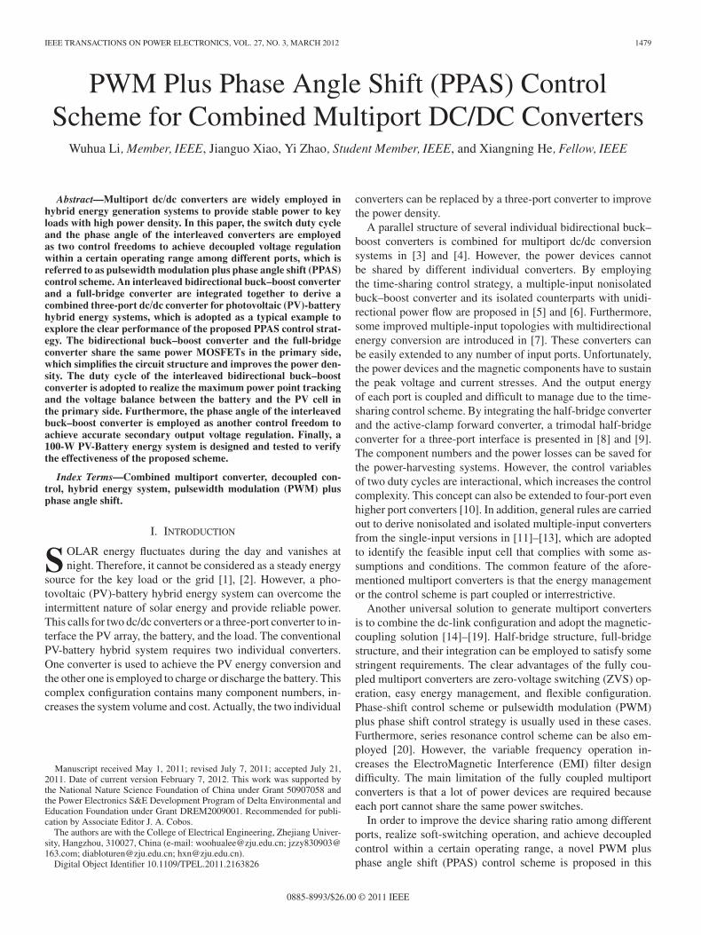
Fig. 3. Key waveforms in battery discharging mode.
n1 turns. The turns ratio N is defined as n2 /n1 . The couplingreference is marked by “∗.” As shown in Fig. 2, vp is the mag-netizing inductor voltage of Tr and Vout is the secondary outputvoltage of the combined three-port converter.
In order to simplify the circuit operation analysis, the magne-tizing inductor of the transformer is assumed to be infinite andall the power devices are ideal. There are two operation modesfor the battery. One is the battery charging mode and the other isthe battery discharging mode. The key steady-state waveformsin the battery discharging mode are shown in Fig. 3. Once in thebattery charging mode, all of the waveforms are nearly the sameexcept that the inductor currents iL 1 and iL 2 change their direc-tions. Therefore, only the battery discharging mode is analyzedhere. There are eight operational stages in one switching period.The corresponding equivalent circuits are shown in Fig. 4.
Stage 1 [t0–t1] [see Fig. 4(a)]: At t0 , S1 is turned ON andS3 remains in ON state. L1 is discharged and L2 is still chargedlinearly. The phase voltage difference vab is Vbus . The leakageinductor current ip increases from the initial value −Ip 0 to zero.Meanwhile, Do 1 and Do2 begin to conduct simultaneously. Themagnetizing inductor voltage vp is zero since the second andthird windings are short circuited. The current through Do 1decreases while that through Do 2 increases. This stage endsuntil ip is zero
ip(t) = −Ip0 +Vbus
LLk· t (1)
t1 − t0 =LLk · Ip0
Vbus. (2)
Fig. 4. Operation stages in battery discharging mode. (a) Stage 1 [t0 –t1 ].(b) Stage 2 [t1 –t2 ]. (c) Stage 3 [t2 –t3 ]. (d) Stage 4 [t3 –t4 ]. (e) Stage 5 [t4 –t5 ].(f) Stage 6 [t5 –t6 ]. (g) Stage 7 [t6 –t7 ]. (h) Stage 8 [t7 –t′0 ].

1482 IEEE TRANSACTIONS ON POWER ELECTRONICS, VOL. 27, NO. 3, MARCH 2012
Stage 2 [t1–t2] [see Fig. 4(b)]: At t1 , the leakage inductorcurrent ip increases from zero. The voltages of vab and vp andthe operational states of all the power devices remain unchanged.The current commutation of Do1 and Do 2 continues until thediode current iDo2 decreases to zero while iDo1 is equal to theoutput filter inductor current iLf
ip(t) =Vbus
LLk· (t − t1). (3)
Stage 3 [t2–t3] [see Fig. 4(c)]: At t2 , Do2 is reverse-biasedand the output filter inductor current iLf fully flows throughDo1 . The leakage inductor current ip is the output filter inductorcurrent iLf divided by N. The primary voltage vab is Vbus , but themagnetizing inductor voltage vp is (Vbus−VLk 1), where VLk 1is given by
VLk1 ≈ LLk
N 2 · Lf(Vbus − N · Vout) (4)
ip(t) = Ip(t2) +VLk1
LLk· (t − t2). (5)
Stage 4 [t3–t4] [see Fig. 4(d)]: At t3 , S3 is turned OFF whileS2 is turned ON. The inductor current iL 2 starts to decrease andthe output filter inductor current begins to freewheel throughDo1 . The primary voltage vab is shorted by S1 and S2 , but themagnetizing inductor voltage vp is equal to the small valueVLk 2 , which is derived by
VLk2 ≈ LLk
N · Lf· Vout (6)
ip(t) = Ip(t3) −VLk2
LLk·(t − ϕ
2π· Ts
). (7)
Stage 5 [t4–t5] [see Fig. 4(e)]: At t4 , S1 is turned OFF whileS4 is turned ON. The inductor current iL 1 starts to increase. Theleakage inductor current ip starts to decrease since the primaryvoltage vab is −Vbus , but the magnetizing inductor voltage vp
is zero. At the same time, Do1 and Do2 begin to conduct simul-taneously. The diode current iDo1 decreases and iDo2 increasesuntil the leakage inductor current ip reduces to zero
ip(t) = Ip(t4) −Vbus
LLk· (t − D · Ts). (8)
Stage 6 [t5–t6] [see Fig. 4(f)]: At t5 , the leakage inductorcurrent ip decreases from zero to a negative value linearly. Do 1and Do2 are still in the conduction state and the diode currentiDo1 decreases to zero
ip(t) = −Vbus
LLk· (t − t5). (9)
Stage 7 [t6–t7] [see Fig. 4(g)]: At t6 , Do1 is blocked and theoutput filter inductor current iLf flows through Do 2 . The primaryvoltage vab is −Vbus and the magnetizing inductor voltage vp
is (−Vbus+VLk 1).
Stage 8 [t7–t′0 ] [see Fig. 4(h)]: At t7 , S2 is turned OFFwhile S3 is turned ON. The inductor current iL 2 starts to in-crease. The primary voltage vab is shorted by S3 and S4 andthe magnetizing inductor voltage vp equals to −VLk 2 . Thisstage ends until S1 is turned ON. Then, a new switching periodbegins.
IV. CIRCUIT PERFORMANCE ANALYSIS
A. Formula Derivation
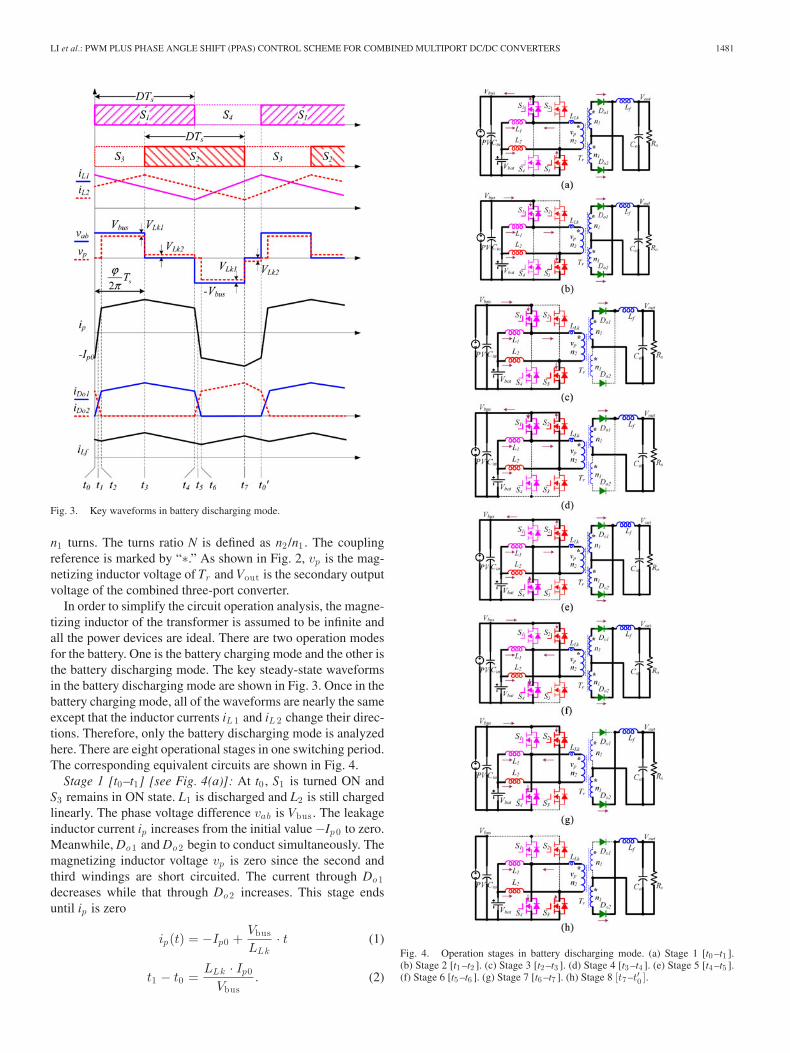
The output filter inductor Lf is assumed to be large enoughand its current ripple is ignored to simplify the voltage gainderivation. The secondary inductor current iLf is equal to theoutput current Io . The variation range of the phase angle ϕ isfrom zero to π. There are three possible operation cases basedon the relationship between the duty cycle D and the phase angleϕ, which are shown in Fig. 5.
Case 1 [(ϕ/2π) < D and (ϕ/2π) < (1 − D)] [see Fig. 5(a)]:During the time interval 0 to Tr , the increment of the leakageinductor current should satisfy the following:
Vbus
LLk· Tr = 2 · Io
N. (10)
The output current can be expressed by
Io =Vout
Ro. (11)
Due to the volt-second balance principle on the output filterinductor, the output voltage can be derived by
Vout =1Ts
∫ Ts
0
|vp |N
dt =2Ts
· Vbus
N·( ϕ
2πTs − Tr
). (12)
From (10) to (12), the output voltage is a function of the phaseangle ϕ, which is obtained by
Vout =2Vbus/N
1 + (4LLk/N 2 · Ro · Ts)
· ϕ
2π
[ ϕ
2π≤ D and
ϕ
2π≤ (1 − D)
]. (13)
Case 2 [D < 0.5 and D < (ϕ/2π) < (1 − D)] [see Fig. 5(b)]:Employing the similar derivation procedure, the output voltagecan be given by
Vout =1Ts
∫ Ts
0
|vp |N
dt =2Ts
· Vbus
N· (D · Ts − Tr ) . (14)
Based on (10), (11), and (14), the output voltage is a functionof the duty cycle D, which is written by
Vout =2Vbus/N
1 + (4LLk/N 2 · Ro · Ts)
· D[D < 0.5 and D <
ϕ
2π< (1 − D)
]. (15)
Case 3 [D > 0.5 and (1 − D) < (ϕ/2π) < D] [seeFig. 5(c)]: Applying a similar mathematical derivation, the out-put voltage is a function of the variable (1−D), which is given
LI et al.: PWM PLUS PHASE ANGLE SHIFT (PPAS) CONTROL SCHEME FOR COMBINED MULTIPORT DC/DC CONVERTERS 1483
Fig. 5. Three operation modes. (a) (ϕ/2π) < D and (ϕ/2π) < (1−D). (b) D <0.5 and D < (ϕ/2π) < (1−D). (c) D > 0.5 and (1−D) < (ϕ/2π) < D.
by
Vout =2Vbus/N
1 + (4LLk/N 2 · Ro · Ts)
· (1 − D)[D > 0.5 and (1 − D) <
ϕ
2π< D
]. (16)
As a result, the general output voltage can be summarized by
Vout =
⎧⎪⎪⎪⎪⎪⎨⎪⎪⎪⎪⎪⎩
G · ϕ
2π· Vbus
[ ϕ
2π≤ D and
ϕ
2π≤ (1−D)
]
G · D · Vbus
[D < 0.5 and D <
ϕ
2π< (1−D)
]
G · (1−D) · Vbus
[D > 0.5 and (1−D) <
ϕ
2π< D
]
(17)
G =2N
· 11 + (4LLk/N 2 · Ro · Ts)
. (18)
From the previous analysis, the duty cycle D can be employedto balance the two primary voltages and the phase angle ϕ isadopted to regulate the secondary output voltage. These twocontrol freedoms make the three-variable system fully control-lable. There is a restrictive condition for the combined three-port converter with the proposed PPAS control scheme, whichis rewritten by
ϕ
2π≤ D and
ϕ
2π≤ (1 − D). (19)
From the general output voltage gain expression shown in(17), it can be determined that the secondary output voltage isdetermined by the switch duty cycle rather than the phase angleif the restrictive condition cannot be satisfied. This means thatthe decoupled control performance is lost. As a result, the dutycycle and the phase angle should be limited to an acceptablerange. Fortunately, this can be easily implemented by the ad-vanced digital signal processor. During the start-up operation, anopen-loop control strategy can be employed before the requiredvoltage is built to guarantee the effective operation.
The primary interleaved buck–boost converter operates in thecontinuous-conduction mode due to the asymmetrical comple-mentary operation of the upper and lower switches. The relation-ship between the battery voltage and the bus voltage is derivedby
Vbat = D · Vbus . (20)
From (17) to (20), the restrictive condition among the bat-tery voltage, bus voltage, and secondary output voltage can beobtained by
Vout ≤ G · Vbat and Vout ≤ G · (Vbus − Vbat). (21)
The voltage stress of the output diodes Do1 and Do 2 is deter-mined by the bus voltage and the turn ratio of the transformer,which is given by
VDo1 = VDo2 =2Vbus
N. (22)
Although a small dc current through the transformer primarywinding may exist due to the potential mismatch of the switchinglegs, it is convenient and effective to balance it by inserting asmall dc block capacitor into the primary winding, which is awidely employed solution in the conventional phase shift full-bridge converters.
1484 IEEE TRANSACTIONS ON POWER ELECTRONICS, VOL. 27, NO. 3, MARCH 2012
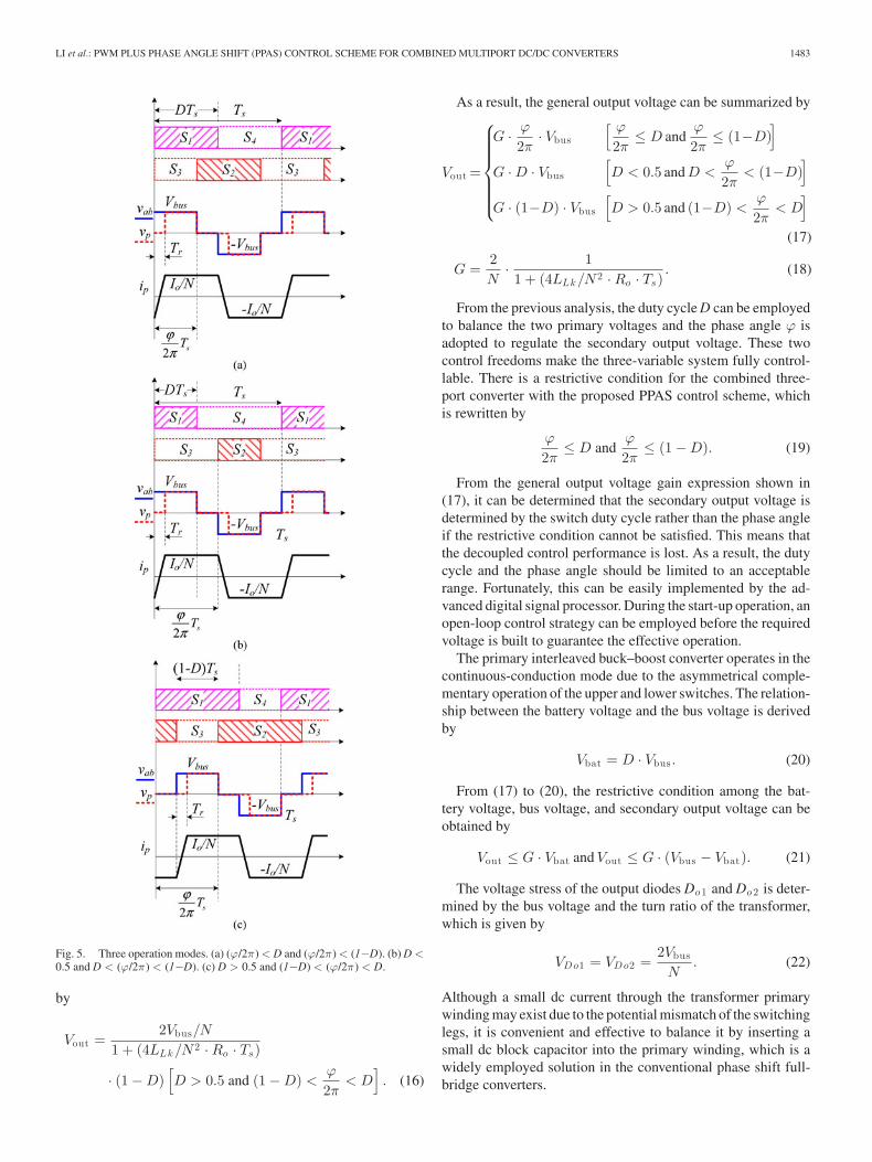
Fig. 6. Operational waveforms with dead time tDT . (a) Simplified primarycircuit. (b) Key waveforms.
B. ZVS Soft-Switching Performance
ZVS soft-switching performance can be achieved due to thephase angle shift control strategy, which is similar to the con-ventional phase shift full-bridge converter. However, due to theexistence of the primary inductors L1 and L2 , ZVS performanceof the combined three-port converter is relatively complicated.ZVS condition of the combined converter is influenced by thefollowing factors: the leakage inductor LLk , the inductor cur-rents iL 1 and iL 2 , the output power of the PV array Pbus , the loadpower Pout , the dead time tDT , and the junction capacitance ofthe switches. By ignoring the current ripple on the output filterinductor Lf , the ideal operation waveforms with an exaggerateddead time tDT are shown in Fig. 6. The currents ILH and ILL
represent the peak and valley values of the inductor current iL 1or iL 2 since the dead time is small enough to ignore the induc-tor current variation during the time interval tDT . The batterydischarging operation is employed as an example to discuss thesoft-switching operation of the proposed converter. Actually,the ZVS range in the battery charging operation is quite simi-lar to that in the battery discharging operation. The followinganalytical procedure and results are universal regardless of theoperation mode.
Once the antiparallel diode of the MOSFET is in the turn-ON state before its turn-ON gate signal comes, ZVS turn-ON isachieved. Therefore, ZVS conditions of the switches S1–S4 canbe derived by
⎧⎪⎪⎪⎪⎪⎨⎪⎪⎪⎪⎪⎩
Ip(tS1) − ILH < 0 for S1
Ip(tS2) + ILH > 0 for S2
Ip(tS3) + ILL < 0 for S3
Ip(tS4) − ILL > 0 for S4
(23)
where Ip (t1) to Ip (t4) are represented by⎧⎪⎪⎪⎪⎪⎪⎪⎪⎪⎪⎪⎨⎪⎪⎪⎪⎪⎪⎪⎪⎪⎪⎪⎩
Ip(tS1) = − Io
N+
Vbus
LLk· tDT
Ip(tS2) =Io
N
Ip(tS3) = − Io
N
Ip(tS4) =Io
N− Vbus
LLk· tDT .
(24)
From (23) and (24), it can be seen that the ZVS condition ofswitches S1 and S4 is more rigorous than that of switches S2 andS3 because the term (Vbus /LLk )·tDT is positive. As a result, theZVS condition of all power MOSFETs can be guaranteed oncethe following is satisfied
⎧⎪⎪⎨⎪⎪⎩
ILH > − Io
N+
Vbus
LLk· tDT
ILL <Io
N− Vbus
LLk· tDT .
(25)
From (25), it can be concluded that the ZVS condition isdetermined by the secondary output current, the turns ratio ofthe transformer, the bus voltage, the leakage inductor, the deadtime, and the current ripple on the primary inductors.
Assuming the circuit conversion efficiency is unity, the peakand the valley current values can be derived by
⎧⎪⎪⎨⎪⎪⎩
ILH =Pout − Pbus
2Vbat+
12· Vbat
L1· (1 − D) · Ts
ILL =Pout − Pbus
2Vbat− 1
2· Vbat
L1· (1 − D) · Ts.
(26)
As a result, the detailed ZVS condition of the combined three-port converter can be represented by
⎧⎪⎪⎪⎪⎪⎪⎪⎪⎪⎪⎪⎪⎪⎨⎪⎪⎪⎪⎪⎪⎪⎪⎪⎪⎪⎪⎪⎩
Pbus <
(1 +
2Vbat
N · Vout
)· Pout +
V 2bat
L1· (1 − D) · Ts
−2Vbat · Vbus
LLk· tDT
Pbus >
(1 − 2Vbat
N · Vout
)· Pout −
V 2bat
L1· (1 − D) · Ts
+2Vbat · Vbus
LLk· tDT .
(27)From (27), the ZVS margin of the combined converter with
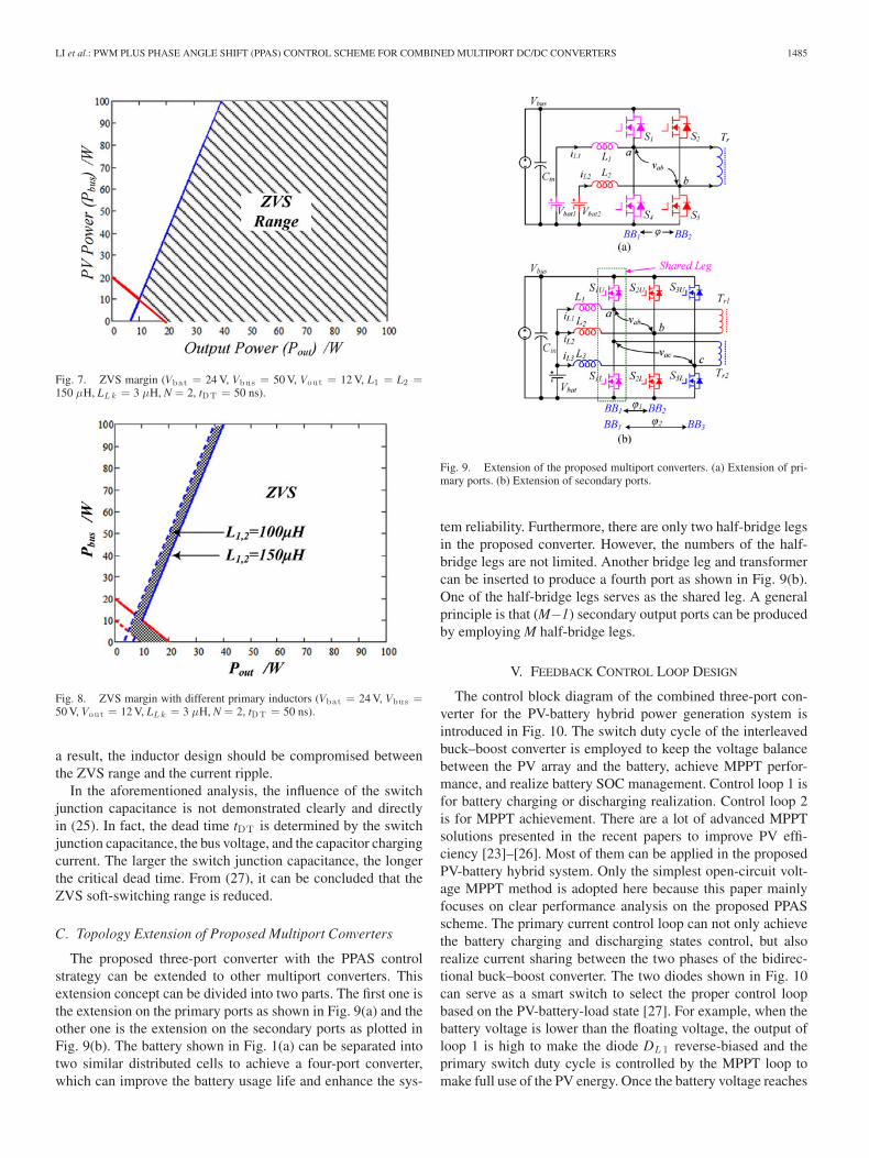
a PPAS control scheme is plotted in Fig. 7, where a PV-batteryhybrid generation system is employed with the following pa-rameters: Vbat = 24 V, Vbus = 50 V, Vout = 12 V, L1 = L2 =150 μH, LLk = 3 μH, N = 2, tDT = 50 ns. A wide-range ZVSoperation can be achieved to improve the circuit efficiency.
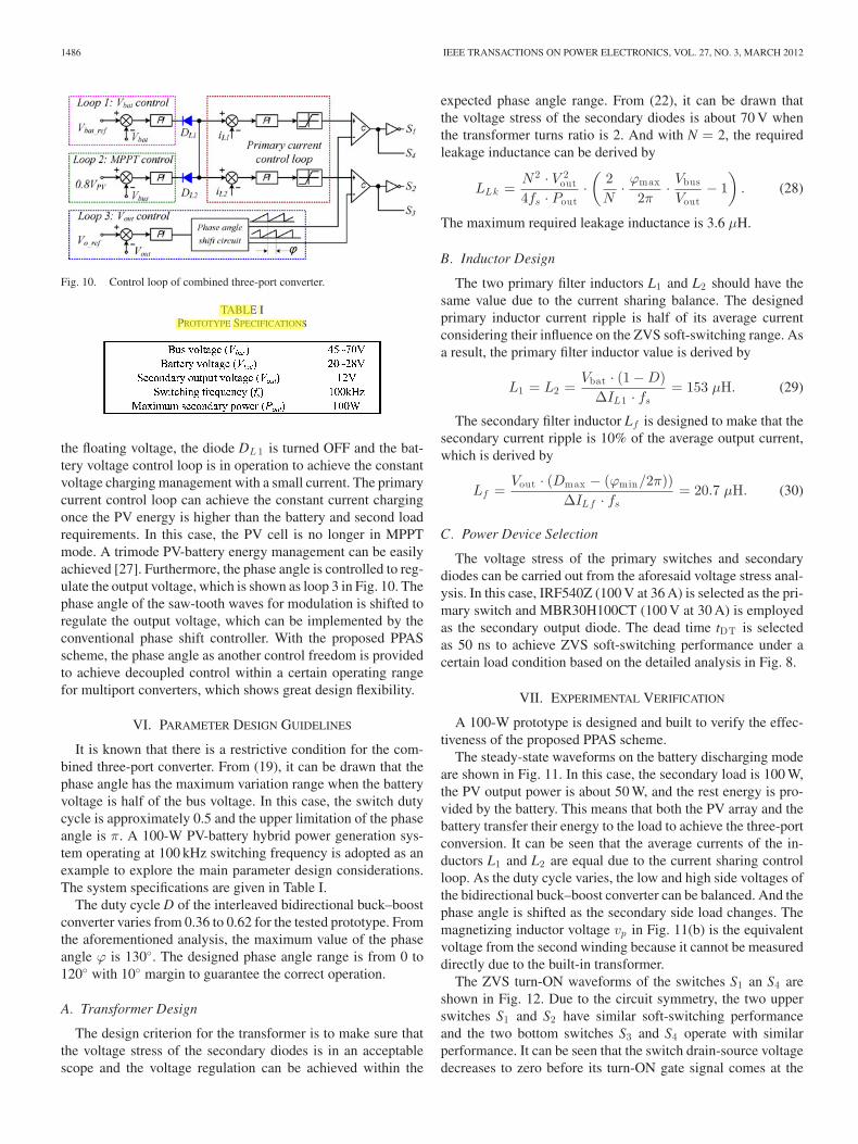
From (27), it can be concluded that the inductors of the bidi-rectional buck–boost converter has a minor impact on the ZVSrange. The ZVS margin of the combined converter with differentinductors is drawn in Fig. 8. ZVS range is extended when theinductors of the bidirectional buck–boost converter decrease. As
LI et al.: PWM PLUS PHASE ANGLE SHIFT (PPAS) CONTROL SCHEME FOR COMBINED MULTIPORT DC/DC CONVERTERS 1485
Fig. 7. ZVS margin (Vbat = 24 V, Vbus = 50 V, Vout = 12 V, L1 = L2 =150 μH, LLk = 3 μH, N = 2, tDT = 50 ns).
Fig. 8. ZVS margin with different primary inductors (Vbat = 24 V, Vbus =50 V, Vout = 12 V, LLk = 3 μH, N = 2, tDT = 50 ns).
a result, the inductor design should be compromised betweenthe ZVS range and the current ripple.
In the aforementioned analysis, the influence of the switchjunction capacitance is not demonstrated clearly and directlyin (25). In fact, the dead time tDT is determined by the switchjunction capacitance, the bus voltage, and the capacitor chargingcurrent. The larger the switch junction capacitance, the longerthe critical dead time. From (27), it can be concluded that theZVS soft-switching range is reduced.
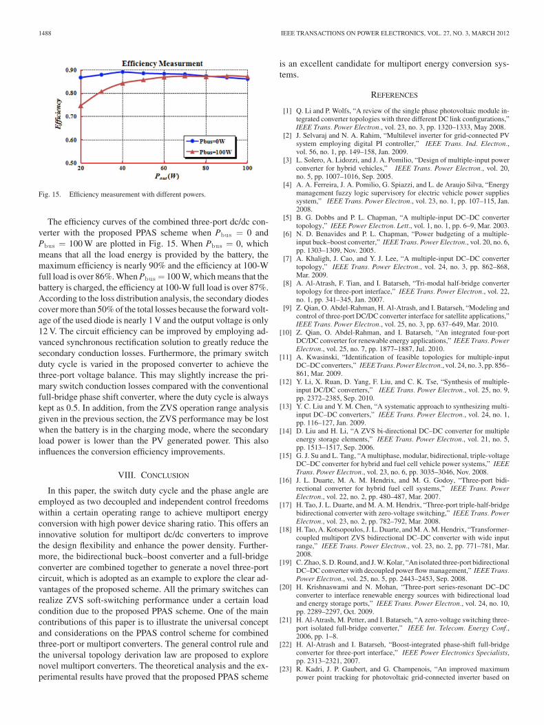
C. Topology Extension of Proposed Multiport Converters
The proposed three-port converter with the PPAS controlstrategy can be extended to other multiport converters. Thisextension concept can be divided into two parts. The first one isthe extension on the primary ports as shown in Fig. 9(a) and theother one is the extension on the secondary ports as plotted inFig. 9(b). The battery shown in Fig. 1(a) can be separated intotwo similar distributed cells to achieve a four-port converter,which can improve the battery usage life and enhance the sys-
Fig. 9. Extension of the proposed multiport converters. (a) Extension of pri-mary ports. (b) Extension of secondary ports.
tem reliability. Furthermore, there are only two half-bridge legsin the proposed converter. However, the numbers of the half-bridge legs are not limited. Another bridge leg and transformercan be inserted to produce a fourth port as shown in Fig. 9(b).One of the half-bridge legs serves as the shared leg. A generalprinciple is that (M−1) secondary output ports can be producedby employing M half-bridge legs.
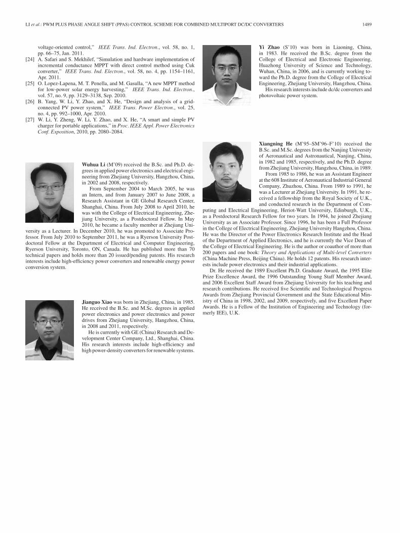
V. FEEDBACK CONTROL LOOP DESIGN
The control block diagram of the combined three-port con-verter for the PV-battery hybrid power generation system isintroduced in Fig. 10. The switch duty cycle of the interleavedbuck–boost converter is employed to keep the voltage balancebetween the PV array and the battery, achieve MPPT perfor-mance, and realize battery SOC management. Control loop 1 isfor battery charging or discharging realization. Control loop 2is for MPPT achievement. There are a lot of advanced MPPTsolutions presented in the recent papers to improve PV effi-ciency [23]–[26]. Most of them can be applied in the proposedPV-battery hybrid system. Only the simplest open-circuit volt-age MPPT method is adopted here because this paper mainlyfocuses on clear performance analysis on the proposed PPASscheme. The primary current control loop can not only achievethe battery charging and discharging states control, but alsorealize current sharing between the two phases of the bidirec-tional buck–boost converter. The two diodes shown in Fig. 10can serve as a smart switch to select the proper control loopbased on the PV-battery-load state [27]. For example, when thebattery voltage is lower than the floating voltage, the output ofloop 1 is high to make the diode DL 1 reverse-biased and theprimary switch duty cycle is controlled by the MPPT loop tomake full use of the PV energy. Once the battery voltage reaches
1486 IEEE TRANSACTIONS ON POWER ELECTRONICS, VOL. 27, NO. 3, MARCH 2012
Fig. 10. Control loop of combined three-port converter.
TABLE IPROTOTYPE SPECIFICATIONS
the floating voltage, the diode DL 1 is turned OFF and the bat-tery voltage control loop is in operation to achieve the constantvoltage charging management with a small current. The primarycurrent control loop can achieve the constant current chargingonce the PV energy is higher than the battery and second loadrequirements. In this case, the PV cell is no longer in MPPTmode. A trimode PV-battery energy management can be easilyachieved [27]. Furthermore, the phase angle is controlled to reg-ulate the output voltage, which is shown as loop 3 in Fig. 10. Thephase angle of the saw-tooth waves for modulation is shifted toregulate the output voltage, which can be implemented by theconventional phase shift controller. With the proposed PPASscheme, the phase angle as another control freedom is providedto achieve decoupled control within a certain operating rangefor multiport converters, which shows great design flexibility.
VI. PARAMETER DESIGN GUIDELINES
It is known that there is a restrictive condition for the com-bined three-port converter. From (19), it can be drawn that thephase angle has the maximum variation range when the batteryvoltage is half of the bus voltage. In this case, the switch dutycycle is approximately 0.5 and the upper limitation of the phaseangle is π. A 100-W PV-battery hybrid power generation sys-tem operating at 100 kHz switching frequency is adopted as anexample to explore the main parameter design considerations.The system specifications are given in Table I.
The duty cycle D of the interleaved bidirectional buck–boostconverter varies from 0.36 to 0.62 for the tested prototype. Fromthe aforementioned analysis, the maximum value of the phaseangle ϕ is 130◦. The designed phase angle range is from 0 to120◦ with 10◦ margin to guarantee the correct operation.
A. Transformer Design
The design criterion for the transformer is to make sure thatthe voltage stress of the secondary diodes is in an acceptablescope and the voltage regulation can be achieved within the
expected phase angle range. From (22), it can be drawn thatthe voltage stress of the secondary diodes is about 70 V whenthe transformer turns ratio is 2. And with N = 2, the requiredleakage inductance can be derived by
LLk =N 2 · V 2
out
4fs · Pout·(
2N
· ϕmax
2π· Vbus
Vout− 1
). (28)
The maximum required leakage inductance is 3.6 μH.
B. Inductor Design
The two primary filter inductors L1 and L2 should have thesame value due to the current sharing balance. The designedprimary inductor current ripple is half of its average currentconsidering their influence on the ZVS soft-switching range. Asa result, the primary filter inductor value is derived by
L1 = L2 =Vbat · (1 − D)
ΔIL1 · fs= 153 μH. (29)
The secondary filter inductor Lf is designed to make that thesecondary current ripple is 10% of the average output current,which is derived by
Lf =Vout · (Dmax − (ϕmin/2π))
ΔILf · fs= 20.7 μH. (30)
C. Power Device Selection
The voltage stress of the primary switches and secondarydiodes can be carried out from the aforesaid voltage stress anal-ysis. In this case, IRF540Z (100 V at 36 A) is selected as the pri-mary switch and MBR30H100CT (100 V at 30 A) is employedas the secondary output diode. The dead time tDT is selectedas 50 ns to achieve ZVS soft-switching performance under acertain load condition based on the detailed analysis in Fig. 8.
VII. EXPERIMENTAL VERIFICATION
A 100-W prototype is designed and built to verify the effec-tiveness of the proposed PPAS scheme.
The steady-state waveforms on the battery discharging modeare shown in Fig. 11. In this case, the secondary load is 100 W,the PV output power is about 50 W, and the rest energy is pro-vided by the battery. This means that both the PV array and thebattery transfer their energy to the load to achieve the three-portconversion. It can be seen that the average currents of the in-ductors L1 and L2 are equal due to the current sharing controlloop. As the duty cycle varies, the low and high side voltages ofthe bidirectional buck–boost converter can be balanced. And thephase angle is shifted as the secondary side load changes. Themagnetizing inductor voltage vp in Fig. 11(b) is the equivalentvoltage from the second winding because it cannot be measureddirectly due to the built-in transformer.
The ZVS turn-ON waveforms of the switches S1 an S4 areshown in Fig. 12. Due to the circuit symmetry, the two upperswitches S1 and S2 have similar soft-switching performanceand the two bottom switches S3 and S4 operate with similarperformance. It can be seen that the switch drain-source voltagedecreases to zero before its turn-ON gate signal comes at the

LI et al.: PWM PLUS PHASE ANGLE SHIFT (PPAS) CONTROL SCHEME FOR COMBINED MULTIPORT DC/DC CONVERTERS 1487
Fig. 11. Steady-state waveforms with Vbus = 50 V, Vbat = 24 V, Pbus =50 W, Pout = 100 W. (a) Effect of current sharing loop. (b) Phase angle shiftwaveforms.
Fig. 12. ZVS-ON performance Vbus = 55 V, Vbat = 20 V, Pbus = 55 W,Pout = 60 W. (a) ZVS-ON waveforms of S1 . (b) ZVS-ON waveforms of S4 .
measured load. As a result, ZVS soft-switching performanceis achieved for all the primary power MOSFETs to reduce theswitching losses.
The critical ZVS operation range of the combined three-portdc/dc converter with the proposed PPAS scheme is plotted inFig. 13. When the PV output power is 10 W and the secondaryload is 12 W, the drain-source voltage of the switch S1 is justreduced to zero at the interval that its turn-ON gate signal isgiven, which means that the combined converter operates in thecritical ZVS state. Furthermore, the ZVS operation of the switchS4 is totally ensured at the critical state. These experimentalresults are consistent with the theoretical analysis in the previoussection.
The experimental waveforms with step load are given inFig. 14, where Vbus ac and Vout ac represent the ac compo-
Fig. 13. Critical ZVS-ON performance Vbus = 55 V, Vbat = 20 V, Pbus =10 W, Pout = 12 W. (a) ZVS-ON waveforms of S1 . (b) ZVS-ON waveforms ofS4 .
Fig. 14. Dynamic response of combined three-port converter with Vbus =50 V, Vbat = 24 V, Pbus = 50 W. (a) Voltage waveforms with ac coupling.(b) Current waveforms.
nents of the voltages Vbus and Vout . The secondary load variesfrom 0.833 to 8.33 A. It can be seen that the transient outputvoltage ripple is small even if a wide-range load variation oc-curs. And the dynamic response of the output voltage is fastalthough the PV output voltage Vbus is a little small with about0.5 V voltage ripple. Due to the decoupled control of the PWMplus phase angle shift control scheme, the dynamic response ofthe bus voltage and the secondary output voltage is independent.
The efficiency of the derived converter is defined by
η =Pout
Pbus + Pbat(31)
where Pout is the secondary load power consumption, Pbus isthe output power of the PV array, and Pbat is the provided orconsumed power of the battery.
1488 IEEE TRANSACTIONS ON POWER ELECTRONICS, VOL. 27, NO. 3, MARCH 2012
Fig. 15. Efficiency measurement with different powers.
The efficiency curves of the combined three-port dc/dc con-verter with the proposed PPAS scheme when Pbus = 0 andPbus = 100 W are plotted in Fig. 15. When Pbus = 0, whichmeans that all the load energy is provided by the battery, themaximum efficiency is nearly 90% and the efficiency at 100-Wfull load is over 86%. When Pbus = 100 W, which means that thebattery is charged, the efficiency at 100-W full load is over 87%.According to the loss distribution analysis, the secondary diodescover more than 50% of the total losses because the forward volt-age of the used diode is nearly 1 V and the output voltage is only12 V. The circuit efficiency can be improved by employing ad-vanced synchronous rectification solution to greatly reduce thesecondary conduction losses. Furthermore, the primary switchduty cycle is varied in the proposed converter to achieve thethree-port voltage balance. This may slightly increase the pri-mary switch conduction losses compared with the conventionalfull-bridge phase shift converter, where the duty cycle is alwayskept as 0.5. In addition, from the ZVS operation range analysisgiven in the previous section, the ZVS performance may be lostwhen the battery is in the charging mode, where the secondaryload power is lower than the PV generated power. This alsoinfluences the conversion efficiency improvements.
VIII. CONCLUSION
In this paper, the switch duty cycle and the phase angle areemployed as two decoupled and independent control freedomswithin a certain operating range to achieve multiport energyconversion with high power device sharing ratio. This offers aninnovative solution for multiport dc/dc converters to improvethe design flexibility and enhance the power density. Further-more, the bidirectional buck–boost converter and a full-bridgeconverter are combined together to generate a novel three-portcircuit, which is adopted as an example to explore the clear ad-vantages of the proposed scheme. All the primary switches canrealize ZVS soft-switching performance under a certain loadcondition due to the proposed PPAS scheme. One of the maincontributions of this paper is to illustrate the universal conceptand considerations on the PPAS control scheme for combinedthree-port or multiport converters. The general control rule andthe universal topology derivation law are proposed to explorenovel multiport converters. The theoretical analysis and the ex-perimental results have proved that the proposed PPAS scheme
is an excellent candidate for multiport energy conversion sys-tems.
REFERENCES
[1] Q. Li and P. Wolfs, “A review of the single phase photovoltaic module in-tegrated converter topologies with three different DC link configurations,”IEEE Trans. Power Electron., vol. 23, no. 3, pp. 1320–1333, May 2008.
[2] J. Selvaraj and N. A. Rahim, “Multilevel inverter for grid-connected PVsystem employing digital PI controller,” IEEE Trans. Ind. Electron.,vol. 56, no. 1, pp. 149–158, Jan. 2009.
[3] L. Solero, A. Lidozzi, and J. A. Pomilio, “Design of multiple-input powerconverter for hybrid vehicles,” IEEE Trans. Power Electron., vol. 20,no. 5, pp. 1007–1016, Sep. 2005.
[4] A. A. Ferreira, J. A. Pomilio, G. Spiazzi, and L. de Araujo Silva, “Energymanagement fuzzy logic supervisory for electric vehicle power suppliessystem,” IEEE Trans. Power Electron., vol. 23, no. 1, pp. 107–115, Jan.2008.
[5] B. G. Dobbs and P. L. Chapman, “A multiple-input DC–DC convertertopology,” IEEE Power Electron. Lett., vol. 1, no. 1, pp. 6–9, Mar. 2003.
[6] N. D. Benavides and P. L. Chapman, “Power budgeting of a multiple-input buck–boost converter,” IEEE Trans. Power Electron., vol. 20, no. 6,pp. 1303–1309, Nov. 2005.
[7] A. Khaligh, J. Cao, and Y. J. Lee, “A multiple-input DC–DC convertertopology,” IEEE Trans. Power Electron., vol. 24, no. 3, pp. 862–868,Mar. 2009.
[8] A. Al-Atrash, F. Tian, and I. Batarseh, “Tri-modal half-bridge convertertopology for three-port interface,” IEEE Trans. Power Electron., vol. 22,no. 1, pp. 341–345, Jan. 2007.
[9] Z. Qian, O. Abdel-Rahman, H. Al-Atrash, and I. Batarseh, “Modeling andcontrol of three-port DC/DC converter interface for satellite applications,”IEEE Trans. Power Electron., vol. 25, no. 3, pp. 637–649, Mar. 2010.
[10] Z. Qian, O. Abdel-Rahman, and I. Batarseh, “An integrated four-portDC/DC converter for renewable energy applications,” IEEE Trans. PowerElectron., vol. 25, no. 7, pp. 1877–1887, Jul. 2010.
[11] A. Kwasinski, “Identification of feasible topologies for multiple-inputDC–DC converters,” IEEE Trans. Power Electron., vol. 24, no. 3, pp. 856–861, Mar. 2009.
[12] Y. Li, X. Ruan, D. Yang, F. Liu, and C. K. Tse, “Synthesis of multiple-input DC/DC converters,” IEEE Trans. Power Electron., vol. 25, no. 9,pp. 2372–2385, Sep. 2010.
[13] Y. C. Liu and Y. M. Chen, “A systematic approach to synthesizing multi-input DC–DC converters,” IEEE Trans. Power Electron., vol. 24, no. 1,pp. 116–127, Jan. 2009.
[14] D. Liu and H. Li, “A ZVS bi-directional DC–DC converter for multipleenergy storage elements,” IEEE Trans. Power Electron., vol. 21, no. 5,pp. 1513–1517, Sep. 2006.
[15] G. J. Su and L. Tang, “A multiphase, modular, bidirectional, triple-voltageDC–DC converter for hybrid and fuel cell vehicle power systems,” IEEETrans. Power Electron., vol. 23, no. 6, pp. 3035–3046, Nov. 2008.
[16] J. L. Duarte, M. A. M. Hendrix, and M. G. Godoy, “Three-port bidi-rectional converter for hybrid fuel cell systems,” IEEE Trans. PowerElectron., vol. 22, no. 2, pp. 480–487, Mar. 2007.
[17] H. Tao, J. L. Duarte, and M. A. M. Hendrix, “Three-port triple-half-bridgebidirectional converter with zero-voltage switching,” IEEE Trans. PowerElectron., vol. 23, no. 2, pp. 782–792, Mar. 2008.
[18] H. Tao, A. Kotsopoulos, J. L. Duarte, and M. A. M. Hendrix, “Transformer-coupled multiport ZVS bidirectional DC–DC converter with wide inputrange,” IEEE Trans. Power Electron., vol. 23, no. 2, pp. 771–781, Mar.2008.
[19] C. Zhao, S. D. Round, and J. W. Kolar, “An isolated three-port bidirectionalDC–DC converter with decoupled power flow management,” IEEE Trans.Power Electron., vol. 25, no. 5, pp. 2443–2453, Sep. 2008.
[20] H. Krishnaswami and N. Mohan, “Three-port series-resonant DC–DCconverter to interface renewable energy sources with bidirectional loadand energy storage ports,” IEEE Trans. Power Electron., vol. 24, no. 10,pp. 2289–2297, Oct. 2009.
[21] H. Al-Atrash, M. Petter, and I. Batarseh, “A zero-voltage switching three-port isolated full-bridge converter,” IEEE Int. Telecom. Energy Conf.,2006, pp. 1–8.
[22] H. Al-Atrash and I. Batarseh, “Boost-integrated phase-shift full-bridgeconverter for three-port interface,” IEEE Power Electronics Specialists,pp. 2313–2321, 2007.
[23] R. Kadri, J. P. Gaubert, and G. Champenois, “An improved maximumpower point tracking for photovoltaic grid-connected inverter based on
LI et al.: PWM PLUS PHASE ANGLE SHIFT (PPAS) CONTROL SCHEME FOR COMBINED MULTIPORT DC/DC CONVERTERS 1489
voltage-oriented control,” IEEE Trans. Ind. Electron., vol. 58, no. 1,pp. 66–75, Jan. 2011.
[24] A. Safari and S. Mekhilef, “Simulation and hardware implementation ofincremental conductance MPPT with direct control method using Cukconverter,” IEEE Trans. Ind. Electron., vol. 58, no. 4, pp. 1154–1161,Apr. 2011.
[25] O. Lopez-Lapena, M. T. Penella, and M. Gasulla, “A new MPPT methodfor low-power solar energy harvesting,” IEEE Trans. Ind. Electron.,vol. 57, no. 9, pp. 3129–3138, Sep. 2010.
[26] B. Yang, W. Li, Y. Zhao, and X. He, “Design and analysis of a grid-connected PV power system,” IEEE Trans. Power Electron., vol. 25,no. 4, pp. 992–1000, Apr. 2010.
[27] W. Li, Y. Zheng, W. Li, Y. Zhao, and X. He, “A smart and simple PVcharger for portable applications,” in Proc. IEEE Appl. Power ElectronicsConf. Exposition, 2010, pp. 2080–2084.
Wuhua Li (M’09) received the B.Sc. and Ph.D. de-grees in applied power electronics and electrical engi-neering from Zhejiang University, Hangzhou, China,in 2002 and 2008, respectively.
From September 2004 to March 2005, he wasan Intern, and from January 2007 to June 2008, aResearch Assistant in GE Global Research Center,Shanghai, China. From July 2008 to April 2010, hewas with the College of Electrical Engineering, Zhe-jiang University, as a Postdoctoral Fellow. In May2010, he became a faculty member at Zhejiang Uni-
versity as a Lecturer. In December 2010, he was promoted to Associate Pro-fessor. From July 2010 to September 2011, he was a Ryerson University Post-doctoral Fellow at the Department of Electrical and Computer Engineering,Ryerson University, Toronto, ON, Canada. He has published more than 70technical papers and holds more than 20 issued/pending patents. His researchinterests include high-efficiency power converters and renewable energy powerconversion system.
Jianguo Xiao was born in Zhejiang, China, in 1985.He received the B.Sc. and M.Sc. degrees in appliedpower electronics and power electronics and powerdrives from Zhejiang University, Hangzhou, China,in 2008 and 2011, respectively.
He is currently with GE (China) Research and De-velopment Center Company, Ltd., Shanghai, China.His research interests include high-efficiency andhigh power-density converters for renewable systems.
Yi Zhao (S’10) was born in Liaoning, China,in 1983. He received the B.Sc. degree from theCollege of Electrical and Electronic Engineering,Huazhong University of Science and Technology,Wuhan, China, in 2006, and is currently working to-ward the Ph.D. degree from the College of ElectricalEngineering, Zhejiang University, Hangzhou, China.
His research interests include dc/dc converters andphotovoltaic power system.
Xiangning He (M’95–SM’96–F’10) received theB.Sc. and M.Sc. degrees from the Nanjing Universityof Aeronautical and Astronautical, Nanjing, China,in 1982 and 1985, respectively, and the Ph.D. degreefrom Zhejiang University, Hangzhou, China, in 1989.
From 1985 to 1986, he was an Assistant Engineerat the 608 Institute of Aeronautical Industrial GeneralCompany, Zhuzhou, China. From 1989 to 1991, hewas a Lecturer at Zhejiang University. In 1991, he re-ceived a fellowship from the Royal Society of U.K.,and conducted research in the Department of Com-
puting and Electrical Engineering, Heriot-Watt University, Edinburgh, U.K.,as a Postdoctoral Research Fellow for two years. In 1994, he joined ZhejiangUniversity as an Associate Professor. Since 1996, he has been a Full Professorin the College of Electrical Engineering, Zhejiang University Hangzhou, China.He was the Director of the Power Electronics Research Institute and the Headof the Department of Applied Electronics, and he is currently the Vice Dean ofthe College of Electrical Engineering. He is the author or coauthor of more than200 papers and one book: Theory and Applications of Multi-level Converters(China Machine Press, Beijing China). He holds 12 patents. His research inter-ests include power electronics and their industrial applications.
Dr. He received the 1989 Excellent Ph.D. Graduate Award, the 1995 ElitePrize Excellence Award, the 1996 Outstanding Young Staff Member Award,and 2006 Excellent Staff Award from Zhejiang University for his teaching andresearch contributions. He received five Scientific and Technological ProgressAwards from Zhejiang Provincial Government and the State Educational Min-istry of China in 1998, 2002, and 2009, respectively, and five Excellent PaperAwards. He is a Fellow of the Institution of Engineering and Technology (for-merly IEE), U.K.