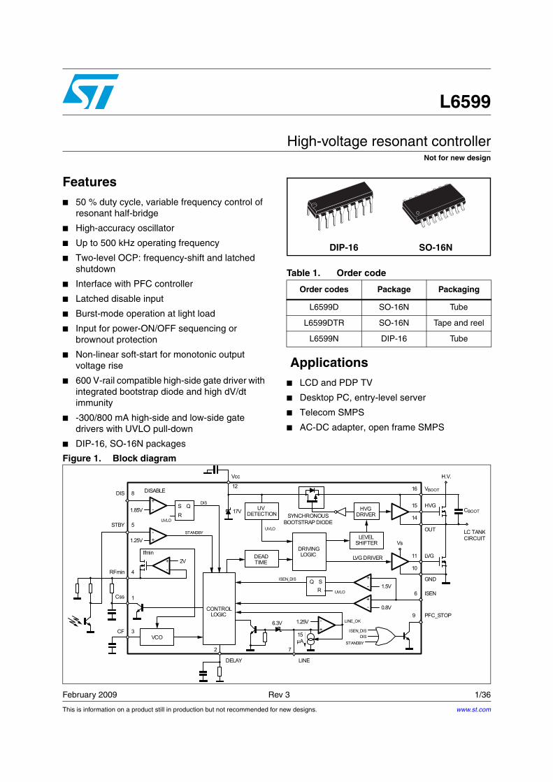
high-voltage resonant controller · lc tank circuit h.v. lvg uv detection vs hvg synchronous...
TRANSCRIPT
Not for new design
This is information on a product still in production but not recommended for new designs.
February 2009 Rev 3 1/36
36
L6599
High-voltage resonant controller
Features■ 50 % duty cycle, variable frequency control of
resonant half-bridge
■ High-accuracy oscillator
■ Up to 500 kHz operating frequency
■ Two-level OCP: frequency-shift and latched shutdown
■ Interface with PFC controller
■ Latched disable input
■ Burst-mode operation at light load
■ Input for power-ON/OFF sequencing or brownout protection
■ Non-linear soft-start for monotonic output voltage rise
■ 600 V-rail compatible high-side gate driver with integrated bootstrap diode and high dV/dt immunity
■ -300/800 mA high-side and low-side gate drivers with UVLO pull-down
■ DIP-16, SO-16N packages
Applications■ LCD and PDP TV
■ Desktop PC, entry-level server
■ Telecom SMPS
■ AC-DC adapter, open frame SMPS
Table 1. Order code
Order codes Package Packaging
L6599D SO-16N Tube
L6599DTR SO-16N Tape and reel
L6599N DIP-16 Tube
DIP-16 SO-16N
www.st.com
Figure 1. Block diagram
STANDBYDIS
ISEN_DIS
GND
Ifmin
ISEN
0.8V
1.5V
PFC_STOP
Vcc
VBOOT
OUT
CBOOT
LC TANKCIRCUIT
H.V.
LVG
UV DETECTION
Vs
HVG
SYNCHRONOUSBOOTSTRAP DIODE
HVG DRIVER
LVG DRIVER
Css
CF
DISABLE
+-
DIS
LINE
DEAD TIME
+-
+-
LEVELSHIFTER
12 8
7
4
3
1
9
6
10
11
14
15
16
RFmin
1.85VS QR
UVLO
UVLO
Q SR UVLO
CONTROLLOGIC
+- LINE_OK1.25V
15µA
DIS
ISEN_DIS
17V
6.3V
VCO
-+1.25V
STANDBY
+-
STBY 5
DRIVING LOGIC
2V
2
DELAY
Contents L6599
2/36
Contents
1 Device description . . . . . . . . . . . . . . . . . . . . . . . . . . . . . . . . . . . . . . . . . . 3
2 Pin settings . . . . . . . . . . . . . . . . . . . . . . . . . . . . . . . . . . . . . . . . . . . . . . . . 4
2.1 Connection . . . . . . . . . . . . . . . . . . . . . . . . . . . . . . . . . . . . . . . . . . . . . . . . . 4
2.2 Functions . . . . . . . . . . . . . . . . . . . . . . . . . . . . . . . . . . . . . . . . . . . . . . . . . . 4
3 Typical system block diagram . . . . . . . . . . . . . . . . . . . . . . . . . . . . . . . . . 6
4 Electrical data . . . . . . . . . . . . . . . . . . . . . . . . . . . . . . . . . . . . . . . . . . . . . . 7
4.1 Maximum ratings . . . . . . . . . . . . . . . . . . . . . . . . . . . . . . . . . . . . . . . . . . . . 7
4.2 Thermal data . . . . . . . . . . . . . . . . . . . . . . . . . . . . . . . . . . . . . . . . . . . . . . . 7
5 Electrical characteristics . . . . . . . . . . . . . . . . . . . . . . . . . . . . . . . . . . . . . 8
6 Typical electrical performance . . . . . . . . . . . . . . . . . . . . . . . . . . . . . . . . 11
7 Application information . . . . . . . . . . . . . . . . . . . . . . . . . . . . . . . . . . . . . 15
7.1 Oscillator . . . . . . . . . . . . . . . . . . . . . . . . . . . . . . . . . . . . . . . . . . . . . . . . . 16
7.2 Operation at no load or very light load . . . . . . . . . . . . . . . . . . . . . . . . . . . 18
7.3 Soft-start . . . . . . . . . . . . . . . . . . . . . . . . . . . . . . . . . . . . . . . . . . . . . . . . . . 21
7.4 Current sense, OCP and OLP . . . . . . . . . . . . . . . . . . . . . . . . . . . . . . . . . 23
7.5 Latched shutdown . . . . . . . . . . . . . . . . . . . . . . . . . . . . . . . . . . . . . . . . . . 27
7.6 Line sensing function . . . . . . . . . . . . . . . . . . . . . . . . . . . . . . . . . . . . . . . . 27
7.7 Bootstrap section . . . . . . . . . . . . . . . . . . . . . . . . . . . . . . . . . . . . . . . . . . . 29
7.8 Application example . . . . . . . . . . . . . . . . . . . . . . . . . . . . . . . . . . . . . . . . . 31
8 Package mechanical data . . . . . . . . . . . . . . . . . . . . . . . . . . . . . . . . . . . . 33
9 Revision history . . . . . . . . . . . . . . . . . . . . . . . . . . . . . . . . . . . . . . . . . . . 35
L6599 Device description
3/36
1 Device description
The L6599 is a double-ended controller specific for the resonant half-bridge topology. It provides 50 % complementary duty cycle: the high-side switch and the low-side switch are driven ON\OFF 180° out-of-phase for exactly the same time. Output voltage regulation is obtained by modulating the operating frequency. A fixed dead-time inserted between the turn-OFF of one switch and the turn-ON of the other one guarantees soft-switching and enables high-frequency operation.
To drive the high-side switch with the bootstrap approach, the IC incorporates a high-voltage floating structure able to withstand more than 600 V with a synchronous-driven high-voltage DMOS that replaces the external fast-recovery bootstrap diode.
The IC enables the designer to set the operating frequency range of the converter by means of an externally programmable oscillator.
At start-up, to prevent uncontrolled inrush current, the switching frequency starts from a programmable maximum value and progressively decays until it reaches the steady-state value determined by the control loop. This frequency shift is non linear to minimize output voltage overshoots; its duration is programmable as well.
The IC can be forced to enter a controlled burst-mode operation at light load, so as to keep converter's input consumption to a minimum.
IC's functions include a not-latched active-low disable input with current hysteresis useful for power sequencing or for brownout protection, a current sense input for OCP with frequency shift and delayed shutdown with automatic restart.
A higher level OCP latches off the IC if the first-level protection is not sufficient to control the primary current. Their combination offers complete protection against overload and short circuits. An additional latched disable input (DIS) allows easy implementation of OTP and/or OVP.
An interface with the PFC controller is provided that enables to switch off the pre-regulator during fault conditions, such as OCP shutdown and DIS high, or during burst-mode operation.
Pin settings L6599
4/36
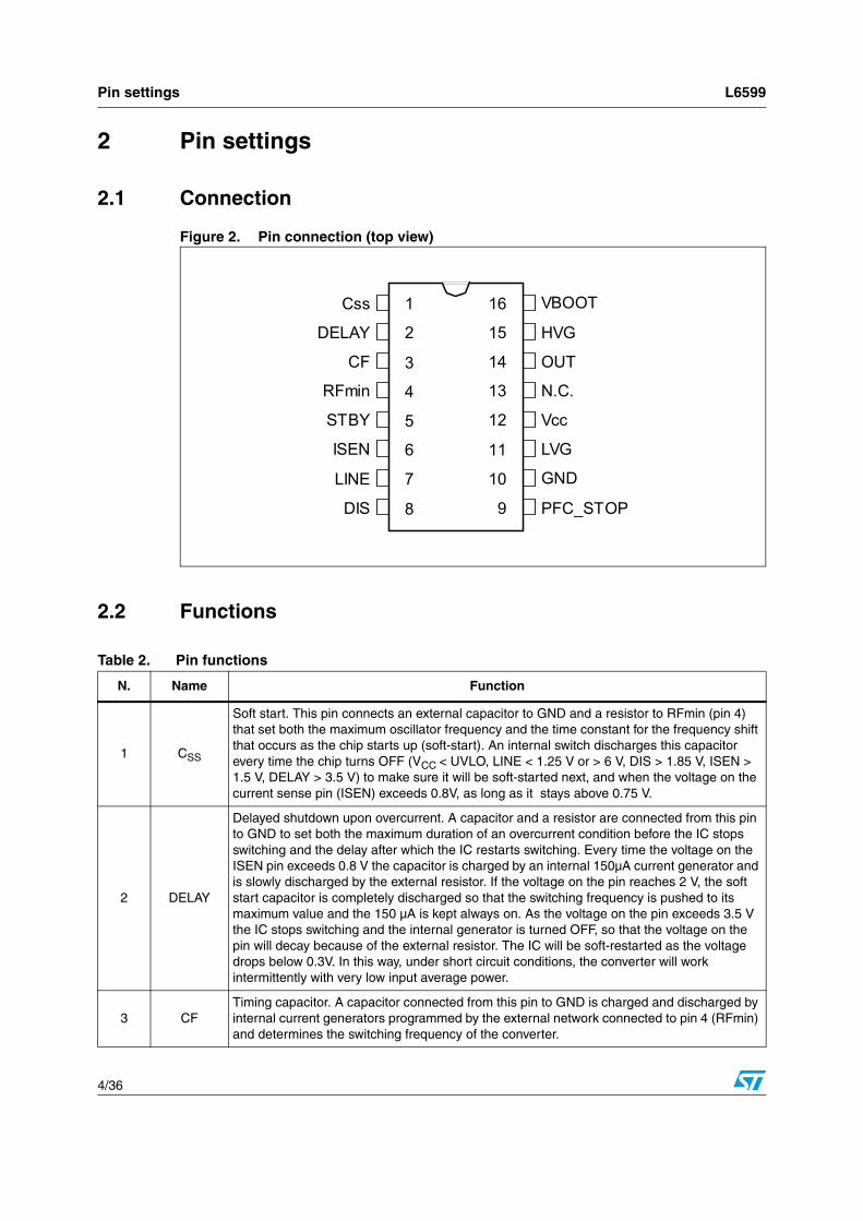
2 Pin settings
2.1 Connection
Figure 2. Pin connection (top view)
2.2 Functions
GND
Css
DELAY
STBY
ISEN
LINE
LVG
VBOOT
HVG
N.C.
Vcc
PFC_STOP
OUT
DIS
CF
RFmin
1
2
3
4
5
6
7
8
16
15
14
13
12
11
10
9
Table 2. Pin functions
N. Name Function
1 CSS
Soft start. This pin connects an external capacitor to GND and a resistor to RFmin (pin 4) that set both the maximum oscillator frequency and the time constant for the frequency shift that occurs as the chip starts up (soft-start). An internal switch discharges this capacitor every time the chip turns OFF (VCC < UVLO, LINE < 1.25 V or > 6 V, DIS > 1.85 V, ISEN >1.5 V, DELAY > 3.5 V) to make sure it will be soft-started next, and when the voltage on the current sense pin (ISEN) exceeds 0.8V, as long as it stays above 0.75 V.
2 DELAY
Delayed shutdown upon overcurrent. A capacitor and a resistor are connected from this pin to GND to set both the maximum duration of an overcurrent condition before the IC stops switching and the delay after which the IC restarts switching. Every time the voltage on the ISEN pin exceeds 0.8 V the capacitor is charged by an internal 150µA current generator and is slowly discharged by the external resistor. If the voltage on the pin reaches 2 V, the soft start capacitor is completely discharged so that the switching frequency is pushed to its maximum value and the 150 µA is kept always on. As the voltage on the pin exceeds 3.5 V the IC stops switching and the internal generator is turned OFF, so that the voltage on the pin will decay because of the external resistor. The IC will be soft-restarted as the voltage drops below 0.3V. In this way, under short circuit conditions, the converter will work intermittently with very low input average power.
3 CFTiming capacitor. A capacitor connected from this pin to GND is charged and discharged by internal current generators programmed by the external network connected to pin 4 (RFmin) and determines the switching frequency of the converter.
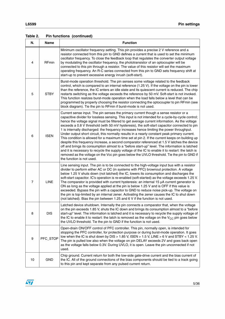
L6599 Pin settings
5/36
N. Name Function
4 RFmin
Minimum oscillator frequency setting. This pin provides a precise 2 V reference and a resistor connected from this pin to GND defines a current that is used to set the minimum oscillator frequency. To close the feedback loop that regulates the converter output voltage by modulating the oscillator frequency, the phototransistor of an optocoupler will be connected to this pin through a resistor. The value of this resistor will set the maximum operating frequency. An R-C series connected from this pin to GND sets frequency shift at start-up to prevent excessive energy inrush (soft-start).
5 STBY
Burst-mode operation threshold. The pin senses some voltage related to the feedback control, which is compared to an internal reference (1.25 V). If the voltage on the pin is lower than the reference, the IC enters an idle state and its quiescent current is reduced. The chip restarts switching as the voltage exceeds the reference by 50 mV. Soft-start is not invoked. This function realizes burst-mode operation when the load falls below a level that can be programmed by properly choosing the resistor connecting the optocoupler to pin RFmin (see block diagram). Tie the pin to RFmin if burst-mode is not used.
6 ISEN
Current sense input. The pin senses the primary current though a sense resistor or a capacitive divider for lossless sensing. This input is not intended for a cycle-by-cycle control; hence the voltage signal must be filtered to get average current information. As the voltage exceeds a 0.8 V threshold (with 50 mV hysteresis), the soft-start capacitor connected to pin 1 is internally discharged: the frequency increases hence limiting the power throughput. Under output short circuit, this normally results in a nearly constant peak primary current. This condition is allowed for a maximum time set at pin 2. If the current keeps on building up despite this frequency increase, a second comparator referenced at 1.5 V latches the device off and brings its consumption almost to a “before start-up” level. The information is latched and it is necessary to recycle the supply voltage of the IC to enable it to restart: the latch is removed as the voltage on the Vcc pin goes below the UVLO threshold. Tie the pin to GND if the function is not used.
7 LINE
Line sensing input. The pin is to be connected to the high-voltage input bus with a resistor divider to perform either AC or DC (in systems with PFC) brownout protection. A voltage below 1.25 V shuts down (not latched) the IC, lowers its consumption and discharges the soft-start capacitor. IC’s operation is re-enabled (soft-started) as the voltage exceeds 1.25 V. The comparator is provided with current hysteresis: an internal 15 µA current generator is ON as long as the voltage applied at the pin is below 1.25 V and is OFF if this value is exceeded. Bypass the pin with a capacitor to GND to reduce noise pick-up. The voltage on the pin is top-limited by an internal zener. Activating the zener causes the IC to shut down (not latched). Bias the pin between 1.25 and 6 V if the function is not used.
8 DIS
Latched device shutdown. Internally the pin connects a comparator that, when the voltage on the pin exceeds 1.85 V, shuts the IC down and brings its consumption almost to a “before start-up” level. The information is latched and it is necessary to recycle the supply voltage of the IC to enable it to restart: the latch is removed as the voltage on the VCC pin goes below the UVLO threshold. Tie the pin to GND if the function is not used.
9 PFC_STOP
Open-drain ON/OFF control of PFC controller. This pin, normally open, is intended for stopping the PFC controller, for protection purpose or during burst-mode operation. It goes low when the IC is shut down by DIS > 1.85 V, ISEN > 1.5 V, LINE > 6 V and STBY < 1.25 V. The pin is pulled low also when the voltage on pin DELAY exceeds 2V and goes back open as the voltage falls below 0.3V. During UVLO, it is open. Leave the pin unconnected if not used.
10 GNDChip ground. Current return for both the low-side gate-drive current and the bias current of the IC. All of the ground connections of the bias components should be tied to a track going to this pin and kept separate from any pulsed current return.
Table 2. Pin functions (continued)
Typical system block diagram L6599
6/36
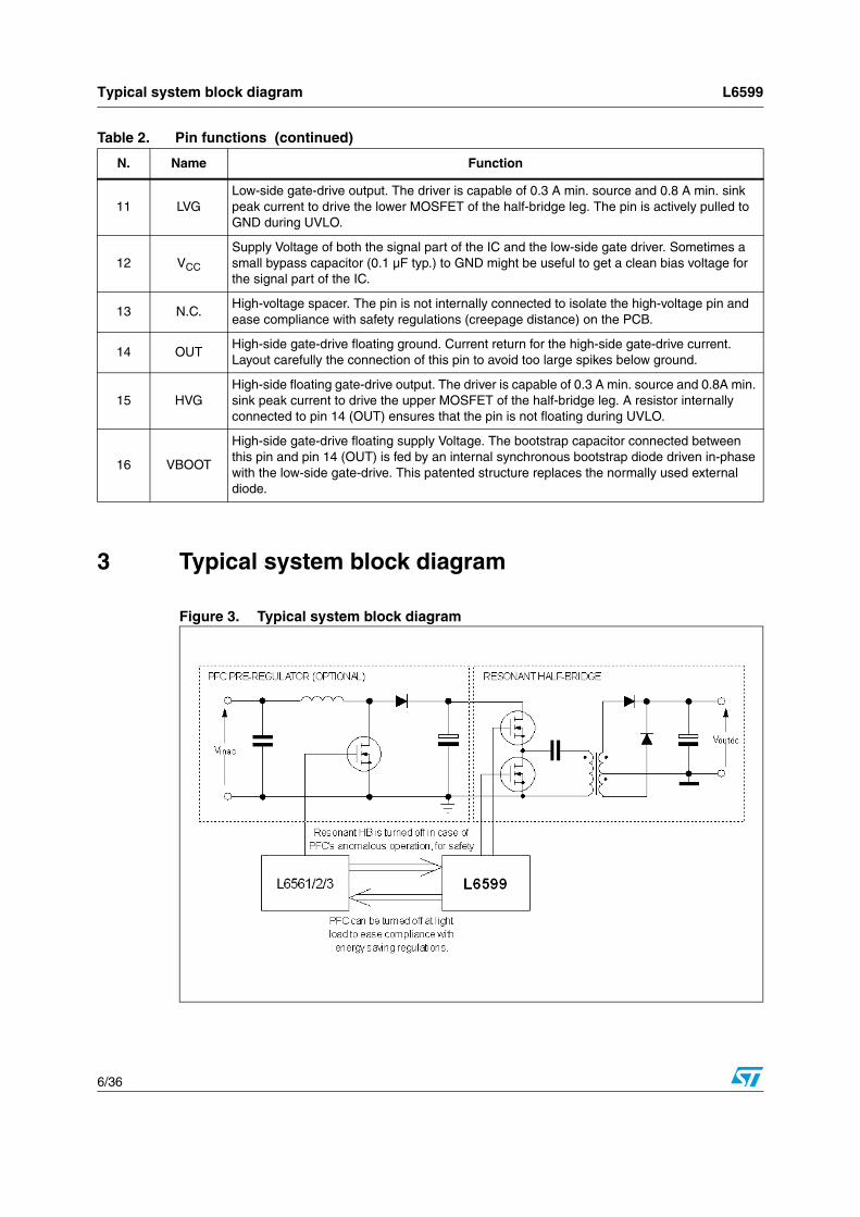
3 Typical system block diagram
Figure 3. Typical system block diagram
N. Name Function
11 LVGLow-side gate-drive output. The driver is capable of 0.3 A min. source and 0.8 A min. sink peak current to drive the lower MOSFET of the half-bridge leg. The pin is actively pulled to GND during UVLO.
12 VCC
Supply Voltage of both the signal part of the IC and the low-side gate driver. Sometimes a small bypass capacitor (0.1 µF typ.) to GND might be useful to get a clean bias voltage for the signal part of the IC.
13 N.C.High-voltage spacer. The pin is not internally connected to isolate the high-voltage pin and ease compliance with safety regulations (creepage distance) on the PCB.
14 OUTHigh-side gate-drive floating ground. Current return for the high-side gate-drive current. Layout carefully the connection of this pin to avoid too large spikes below ground.
15 HVGHigh-side floating gate-drive output. The driver is capable of 0.3 A min. source and 0.8A min. sink peak current to drive the upper MOSFET of the half-bridge leg. A resistor internally connected to pin 14 (OUT) ensures that the pin is not floating during UVLO.
16 VBOOT
High-side gate-drive floating supply Voltage. The bootstrap capacitor connected between this pin and pin 14 (OUT) is fed by an internal synchronous bootstrap diode driven in-phase with the low-side gate-drive. This patented structure replaces the normally used external diode.
Table 2. Pin functions (continued)
L6599 Electrical data
7/36
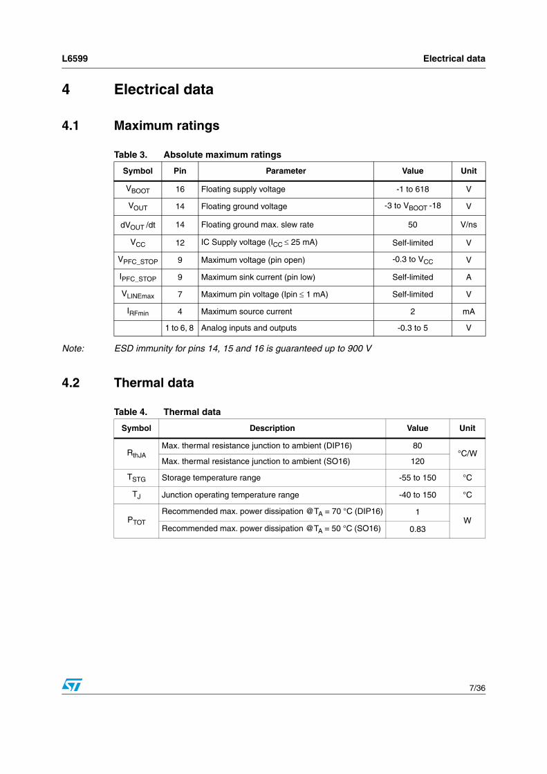
4 Electrical data
4.1 Maximum ratings
Note: ESD immunity for pins 14, 15 and 16 is guaranteed up to 900 V
4.2 Thermal data
Table 3. Absolute maximum ratings
Symbol Pin Parameter Value Unit
VBOOT 16 Floating supply voltage -1 to 618 V
VOUT 14 Floating ground voltage -3 to VBOOT -18 V
dVOUT /dt 14 Floating ground max. slew rate 50 V/ns
VCC 12 IC Supply voltage (ICC ≤ 25 mA) Self-limited V
VPFC_STOP 9 Maximum voltage (pin open) -0.3 to VCC V
IPFC_STOP 9 Maximum sink current (pin low) Self-limited A
VLINEmax 7 Maximum pin voltage (Ipin ≤ 1 mA) Self-limited V
IRFmin 4 Maximum source current 2 mA
1 to 6, 8 Analog inputs and outputs -0.3 to 5 V
Table 4. Thermal data
Symbol Description Value Unit
RthJAMax. thermal resistance junction to ambient (DIP16) 80
°C/WMax. thermal resistance junction to ambient (SO16) 120
TSTG Storage temperature range -55 to 150 °C
TJ Junction operating temperature range -40 to 150 °C
PTOT Recommended max. power dissipation @TA = 70 °C (DIP16) 1
W Recommended max. power dissipation @TA = 50 °C (SO16) 0.83
Electrical characteristics L6599
8/36
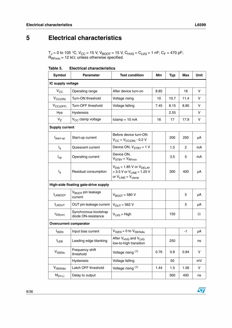
5 Electrical characteristics
TJ = 0 to 105 °C, VCC = 15 V, VBOOT = 15 V, CHVG = CLVG = 1 nF; CF = 470 pF; RRFmin = 12 kΩ; unless otherwise specified.
Table 5. Electrical characteristics
Symbol Parameter Test condition Min Typ Max Unit
IC supply voltage
VCC Operating range After device turn-on 8.85 16 V
VCC(ON) Turn-ON threshold Voltage rising 10 10.7 11.4 V
VCC(OFF) Turn-OFF threshold Voltage falling 7.45 8.15 8.85 V
Hys Hysteresis 2.55 V
VZ VCC clamp voltage Iclamp = 10 mA 16 17 17.9 V
Supply current
Istart-up Start-up current Before device turn-ON VCC = VCC(ON) - 0.2 V
200 250 µA
Iq Quiescent current Device ON, VSTBY = 1 V 1.5 2 mA
Iop Operating current Device ON, VSTBY = VRFmin
3.5 5 mA
Iq Residual consumption VDIS
> 1.85 V or VDELAY > 3.5 V or VLINE < 1.25 V or VLINE = Vclamp
300 400 µA
High-side floating gate-drive supply
ILKBOOTVBOOT pin leakage current
VBOOT = 580 V 5 µA
ILKOUT OUT pin leakage current VOUT = 562 V 5 µA
rDS(on)Synchronous bootstrap diode ON-resistance VLVG
= High 150 Ω
Overcurrent comparator
IISEN Input bias current VISEN = 0 to VISENdis -1 µA
tLEB Leading edge blanking After VHVG and VLVG low-to-high transition
250 ns
VISENxFrequency shift threshold Voltage rising (1) 0.76 0.8 0.84 V
Hysteresis Voltage falling 50 mV
VISENdis Latch OFF threshold Voltage rising (1) 1.44 1.5 1.56 V
td(H-L) Delay to output 300 400 ns
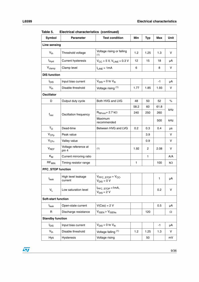
L6599 Electrical characteristics
9/36
Symbol Parameter Test condition Min Typ Max Unit
Line sensing
Vth Threshold voltage Voltage rising or falling (1)
1.2 1.25 1.3 V
IHyst Current hysteresis VCC > 5 V, VLINE = 0.3 V 12 15 18 µA
Vclamp Clamp level ILINE = 1mA 6 8 V
DIS function
IDIS Input bias current VDIS = 0 to Vth -1 µA
Vth Disable threshold Voltage rising (1) 1.77 1.85 1.93 V
Oscillator
D Output duty cycle Both HVG and LVG 48 50 52 %
fosc Oscillation frequency
58.2 60 61.8 kHz
RRFmin= 2.7 kΩ 240 250 260
Maximum recommended
500 kHz
TD Dead-time Between HVG and LVG 0.2 0.3 0.4 µs
VCFp Peak value 3.9 V
VCFv Valley value 0.9 V
VREFVoltage reference at pin 4
(1) 1.92 2 2.08 V
KM Current mirroring ratio 1 A/A
RFMIN Timing resistor range 1 100 kΩ
PFC_STOP function
IleakHigh level leakage current
VPFC_STOP = VCC,
VDIS = 0 V1 µA
VL Low saturation level IPFC_STOP
=1mA,VDIS = 2 V
0.2 V
Soft-start function
Ileak Open-state current V(Css) = 2 V 0.5 µA
R Discharge resistance VISEN > VISENx 120 Ω
Standby function
IDIS Input bias current VDIS = 0 to Vth -1 µA
Vth Disable threshold Voltage falling (1) 1.2 1.25 1.3 V
Hys Hysteresis Voltage rising 50 mV
Table 5. Electrical characteristics (continued)
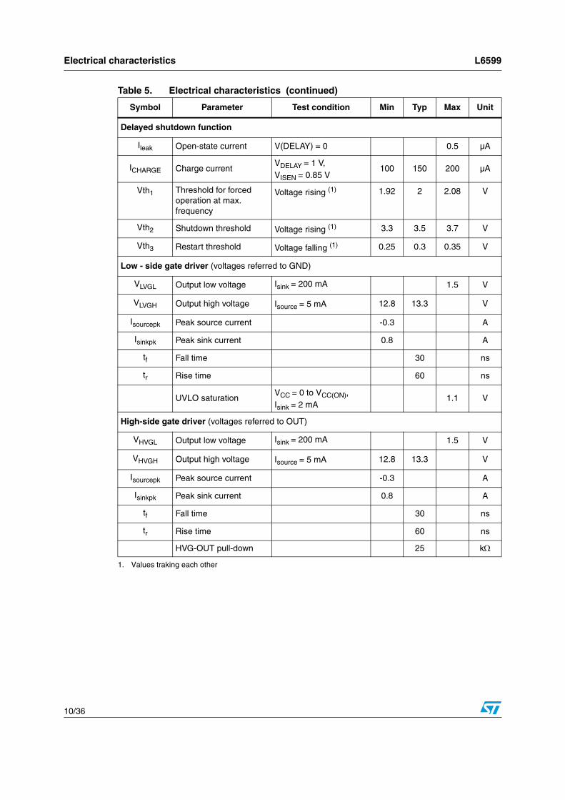
Electrical characteristics L6599
10/36
Symbol Parameter Test condition Min Typ Max Unit
Delayed shutdown function
Ileak Open-state current V(DELAY) = 0 0.5 µA
ICHARGE Charge current VDELAY = 1 V, VISEN = 0.85 V
100 150 200 µA
Vth1 Threshold for forced operation at max. frequency
Voltage rising (1) 1.92 2 2.08 V
Vth2 Shutdown threshold Voltage rising (1) 3.3 3.5 3.7 V
Vth3 Restart threshold Voltage falling (1) 0.25 0.3 0.35 V
Low - side gate driver (voltages referred to GND)
VLVGL Output low voltage Isink = 200 mA 1.5 V
VLVGH Output high voltage Isource = 5 mA 12.8 13.3 V
Isourcepk Peak source current -0.3 A
Isinkpk Peak sink current 0.8 A
tf Fall time 30 ns
tr Rise time 60 ns
UVLO saturation VCC = 0 to VCC(ON), Isink = 2 mA
1.1 V
High-side gate driver (voltages referred to OUT)
VHVGL Output low voltage Isink = 200 mA 1.5 V
VHVGH Output high voltage Isource = 5 mA 12.8 13.3 V
Isourcepk Peak source current -0.3 A
Isinkpk Peak sink current 0.8 A
tf Fall time 30 ns
tr Rise time 60 ns
HVG-OUT pull-down 25 kΩ
1. Values traking each other
Table 5. Electrical characteristics (continued)
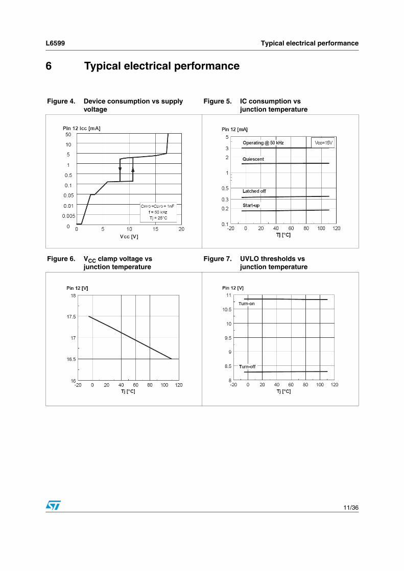
L6599 Typical electrical performance
11/36
6 Typical electrical performance
Figure 4. Device consumption vs supply voltage
Figure 5. IC consumption vs junction temperature
Figure 6. VCC clamp voltage vs junction temperature
Figure 7. UVLO thresholds vs junction temperature
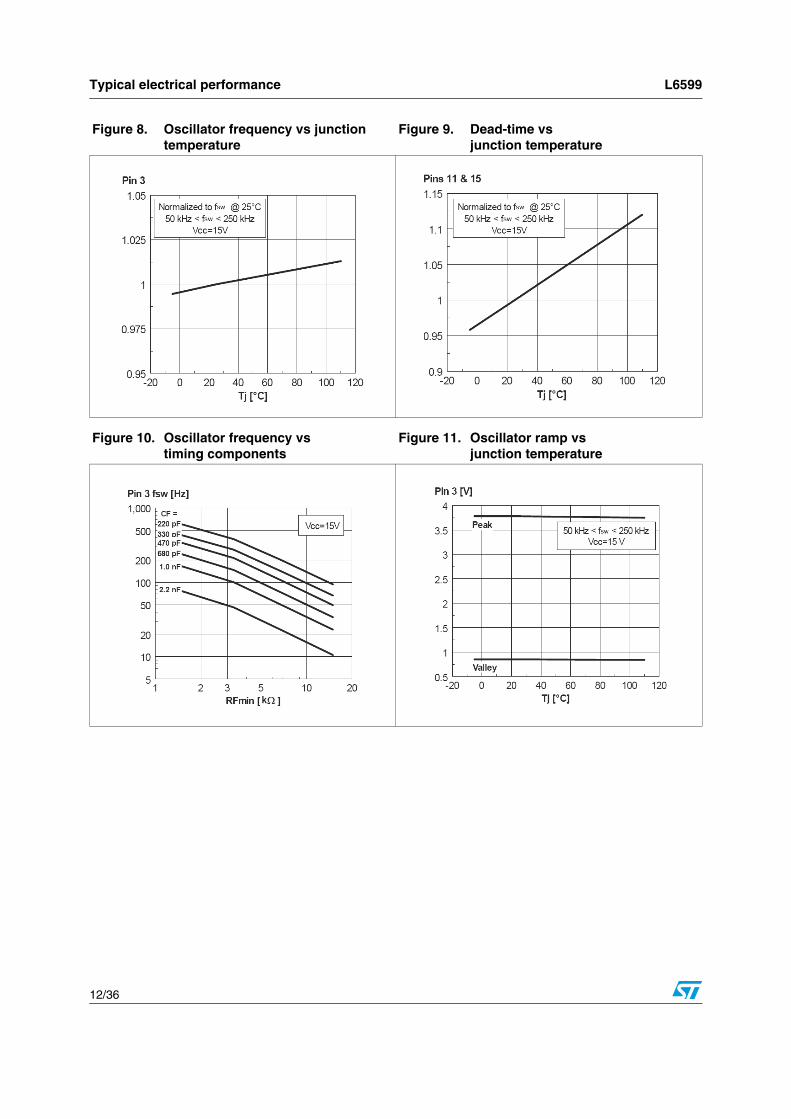
Typical electrical performance L6599
12/36
Figure 8. Oscillator frequency vs junction temperature
Figure 9. Dead-time vs junction temperature
Figure 10. Oscillator frequency vs timing components
Figure 11. Oscillator ramp vs junction temperature
L6599 Typical electrical performance
13/36
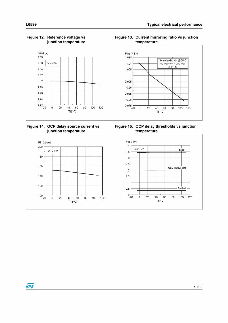
Figure 12. Reference voltage vs junction temperature
Figure 13. Current mirroring ratio vs junction temperature
Figure 14. OCP delay source current vs junction temperature
Figure 15. OCP delay thresholds vs junction temperature
Typical electrical performance L6599
14/36
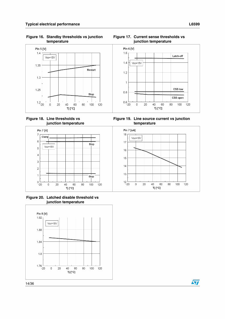
Figure 16. Standby thresholds vs junction temperature
Figure 17. Current sense thresholds vs junction temperature
Figure 18. Line thresholds vs junction temperature
Figure 19. Line source current vs junction temperature
Figure 20. Latched disable threshold vs junction temperature
L6599 Application information
15/36
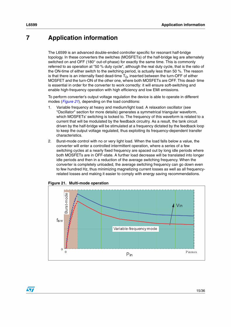
7 Application information
The L6599 is an advanced double-ended controller specific for resonant half-bridge topology. In these converters the switches (MOSFETs) of the half-bridge leg are alternately switched on and OFF (180° out-of-phase) for exactly the same time. This is commonly referred to as operation at "50 % duty cycle", although the real duty cycle, that is the ratio of the ON-time of either switch to the switching period, is actually less than 50 %. The reason is that there is an internally fixed dead-time TD, inserted between the turn-OFF of either MOSFET and the turn-ON of the other one, where both MOSFETs are OFF. This dead- time is essential in order for the converter to work correctly: it will ensure soft-switching and enable high-frequency operation with high efficiency and low EMI emissions.
To perform converter's output voltage regulation the device is able to operate in different modes (Figure 21), depending on the load conditions:
1. Variable frequency at heavy and medium/light load. A relaxation oscillator (see "Oscillator" section for more details) generates a symmetrical triangular waveform, which MOSFETs' switching is locked to. The frequency of this waveform is related to a current that will be modulated by the feedback circuitry. As a result, the tank circuit driven by the half-bridge will be stimulated at a frequency dictated by the feedback loop to keep the output voltage regulated, thus exploiting its frequency-dependent transfer characteristics.
2. Burst-mode control with no or very light load. When the load falls below a value, the converter will enter a controlled intermittent operation, where a series of a few switching cycles at a nearly fixed frequency are spaced out by long idle periods where both MOSFETs are in OFF-state. A further load decrease will be translated into longer idle periods and then in a reduction of the average switching frequency. When the converter is completely unloaded, the average switching frequency can go down even to few hundred Hz, thus minimizing magnetizing current losses as well as all frequency-related losses and making it easier to comply with energy saving recommendations.
Figure 21. Multi-mode operation
Application information L6599
16/36
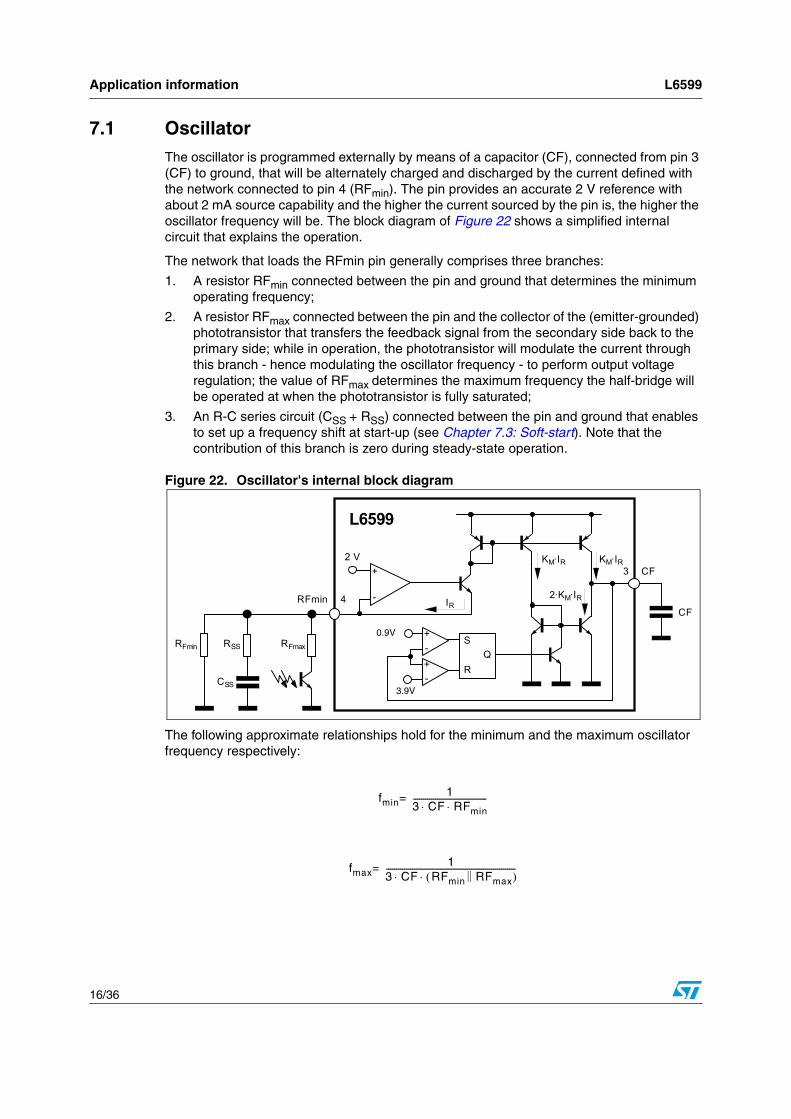
7.1 Oscillator The oscillator is programmed externally by means of a capacitor (CF), connected from pin 3 (CF) to ground, that will be alternately charged and discharged by the current defined with the network connected to pin 4 (RFmin). The pin provides an accurate 2 V reference with about 2 mA source capability and the higher the current sourced by the pin is, the higher the oscillator frequency will be. The block diagram of Figure 22 shows a simplified internal circuit that explains the operation.
The network that loads the RFmin pin generally comprises three branches:
1. A resistor RFmin connected between the pin and ground that determines the minimum operating frequency;
2. A resistor RFmax connected between the pin and the collector of the (emitter-grounded) phototransistor that transfers the feedback signal from the secondary side back to the primary side; while in operation, the phototransistor will modulate the current through this branch - hence modulating the oscillator frequency - to perform output voltage regulation; the value of RFmax determines the maximum frequency the half-bridge will be operated at when the phototransistor is fully saturated;
3. An R-C series circuit (CSS + RSS) connected between the pin and ground that enables to set up a frequency shift at start-up (see Chapter 7.3: Soft-start). Note that the contribution of this branch is zero during steady-state operation.
Figure 22. Oscillator's internal block diagram
The following approximate relationships hold for the minimum and the maximum oscillator frequency respectively:
L6599
2 V+
-4RFmin
3 CF
S QR
+-
1 V
4 V
+-
CFIR
2·KM·IR
KM·IR
RFmin RFmaxRSS
CSS
KM·IR
0.9V
3.9V
fmin1
3 CF RFmin⋅ ⋅-------------------------------------=
fmax1
3 CF RFmin RFmax||( )⋅ ⋅-----------------------------------------------------------------=
L6599 Application information
17/36
After fixing CF in the hundred pF or in the nF (consistently with the maximum source capability of the RFmin pin and trading this off against the total consumption of the device), the value of RFmin and RFmax will be selected so that the oscillator frequency is able to cover the entire range needed for regulation, from the minimum value fmin (at minimum input voltage and maximum load) to the maximum value fmax (at maximum input voltage and minimum load):
A different selection criterion will be given for RFmax in case burst-mode operation at no-load will be used (see "Operation at no load or very light load" section).
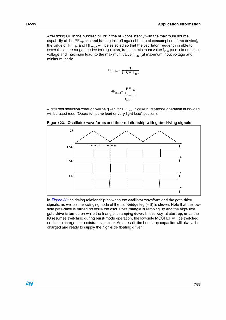
Figure 23. Oscillator waveforms and their relationship with gate-driving signals
In Figure 23 the timing relationship between the oscillator waveform and the gate-drive signals, as well as the swinging node of the half-bridge leg (HB) is shown. Note that the low-side gate-drive is turned on while the oscillator's triangle is ramping up and the high-side gate-drive is turned on while the triangle is ramping down. In this way, at start-up, or as the IC resumes switching during burst-mode operation, the low-side MOSFET will be switched on first to charge the bootstrap capacitor. As a result, the bootstrap capacitor will always be charged and ready to supply the high-side floating driver.
RFmin1
3 CF fmin⋅ ⋅------------------------------=
RFmaxRFmin
fmax
fmin----------- 1–
---------------------=
CF
HVG t
t
LVG t
HB
t
TD TD
Application information L6599
18/36
7.2 Operation at no load or very light loadWhen the resonant half-bridge is lightly loaded or unloaded at all, its switching frequency will be at its maximum value. To keep the output voltage under control in these conditions and to avoid losing soft-switching, there must be some significant residual current flowing through the transformer's magnetizing inductance. This current, however, produces some associated losses that prevent converter's no-load consumption from achieving very low values.
To overcome this issue, the L6599 enables the designer to make the converter operate intermittently (burst-mode operation), with a series of a few switching cycles spaced out by long idle periods where both MOSFETs are in OFF-state, so that the average switching frequency can be substantially reduced. As a result, the average value of the residual magnetizing current and the associated losses will be considerably cut down, thus facilitating the converter to comply with energy saving recommendations.
The device can be operated in burst-mode by using pin 5 (STBY): if the voltage applied to this pin falls below 1.25 V the IC will enter an idle state where both gate-drive outputs are low, the oscillator is stopped, the soft-start capacitor CSS keeps its charge and only the 2 V reference at RFmin pin stays alive to minimize IC's consumption and VCC capacitor's discharge. The IC will resume normal operation as the voltage on the pin exceeds 1.25 V by 50 mV.
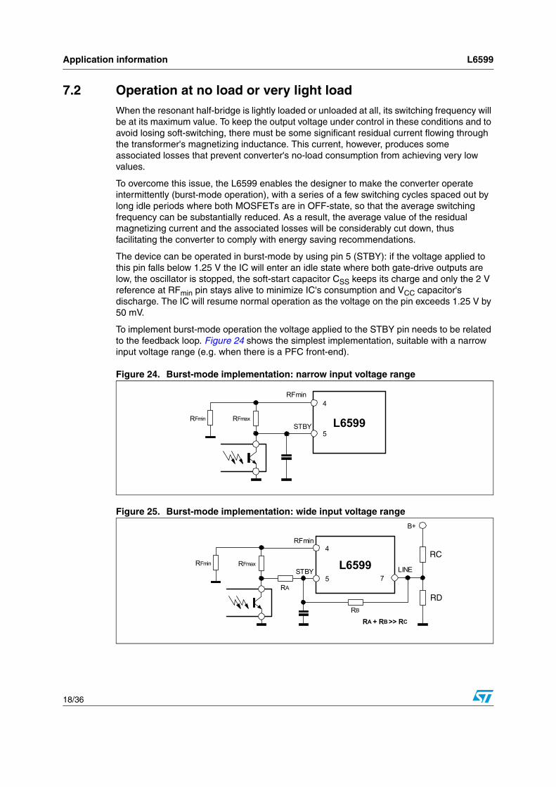
To implement burst-mode operation the voltage applied to the STBY pin needs to be related to the feedback loop. Figure 24 shows the simplest implementation, suitable with a narrow input voltage range (e.g. when there is a PFC front-end).
Figure 24. Burst-mode implementation: narrow input voltage range
Figure 25. Burst-mode implementation: wide input voltage range
L6599STBY
4
5
RFmin
RFmin RFmax RFmin RFmax
L6599 L6599STBY
4
5
RFmin
RFmin RFmax
7LINE
RA
B+
RB
RC
RD
RA + RB >> RC
RC
RD
L6599 Application information
19/36
Essentially, RFmax will define the switching frequency fmax above which the L6599 will enter burst-mode operation. Once fixed fmax, RFmax will be found from the relationship:
Note that, unlike the fmax considered in the previous section ("Chapter 7.1: Oscillator"), here fmax is associated to some load PoutB greater than the minimum one. PoutB will be such that the transformer's peak currents are low enough not to cause audible noise.
Resonant converter's switching frequency, however, depends also on the input voltage; hence, in case there is quite a large input voltage range with the circuit of Figure 24 the value of PoutB would change considerably. In this case it is recommended to use the arrangement shown in Figure 25 where the information on the converter's input voltage is added to the voltage applied to the STBY pin. Due to the strongly non-linear relationship between switching frequency and input voltage, it is more practical to find empirically the right amount of correction RA / (RA + RB) needed to minimize the change of PoutB. Just be careful in choosing the total value RA + RB much greater than RC to minimize the effect on the LINE pin voltage (see Chapter 7.6: Line sensing function).
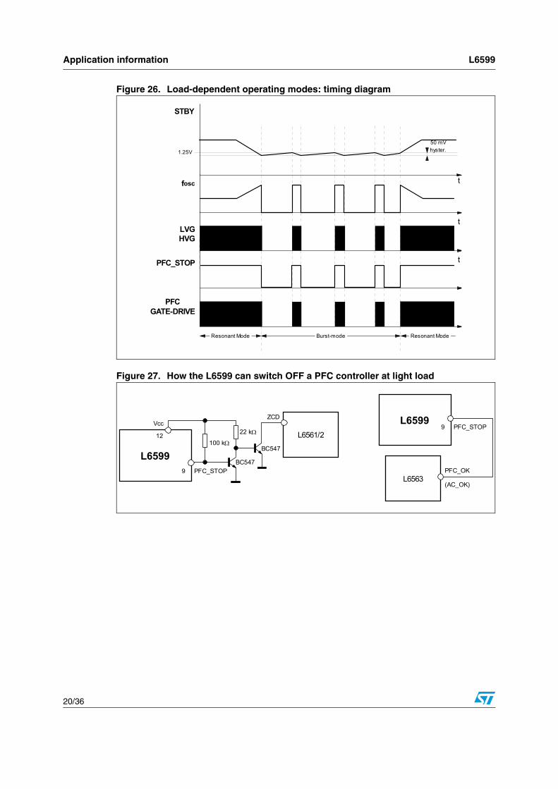
Whichever circuit is in use, its operation can be described as follows. As the load falls below the value PoutB the frequency will try to exceed the maximum programmed value fmax and the voltage on the STBY pin (VSTBY) will go below 1.25V. The IC will then stop with both gate-drive outputs low, so that both MOSFETs of the half-bridge leg are in OFF-state. The voltage VSTBY will now increase as a result of the feedback reaction to the energy delivery stop and, as it exceeds 1.3V, the IC will restart switching. After a while, VSTBY will go down again in response to the energy burst and stop the IC. In this way the converter will work in a burst-mode fashion with a nearly constant switching frequency. A further load decrease will then cause a frequency reduction, which can go down even to few hundred hertz. The timing diagram of Figure 26 illustrates this kind of operation, showing the most significant signals. A small capacitor (typically in the hundred pF) from the STBY pin to ground, placed as close to the IC as possible to reduce switching noise pick-up, will help get clean operation.
To help the designer meet energy saving requirements even in power-factor-corrected systems, where a PFC pre-regulator precedes the DC-DC converter, the device allows that the PFC pre-regulator can be turned off during burst-mode operation, hence eliminating the no-load consumption of this stage (0.5 ÷ 1 W). There is no compliance issue in that because EMC regulations on low-frequency harmonic emissions refer to nominal load, no limit is envisaged when the converter operates with light or no load.
To do so, the device provides pin 9 (PFC_STOP): it is an open collector output, normally open, that is asserted low when the IC is idle during burst-mode operation. This signal will be externally used for switching off the PFC controller and the pre-regulator as shown in Figure 27 When the L6599 is in UVLO the pin is kept open, to let the PFC controller start first.
RFmax38---
RFmin
fmax
fmin----------- 1–
---------------------⋅=
Application information L6599
20/36
Figure 26. Load-dependent operating modes: timing diagram
Figure 27. How the L6599 can switch OFF a PFC controller at light load
LVGHVG
1.25V
t
t
t
STBY
50 mVhyster.
Resonant Mode Burst-mode
fosc
Resonant Mode
PFC_STOP
PFCGATE-DRIVE
L6599PFC_STOP9
L6561/212
VccZCD
22 kΩ
100 kΩ
BC547
BC547
L6599PFC_STOP9
L6563PFC_OK
(AC_OK)
L6599 Application information
21/36
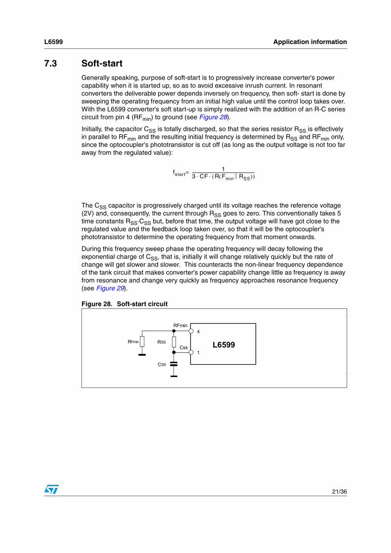
7.3 Soft-startGenerally speaking, purpose of soft-start is to progressively increase converter's power capability when it is started up, so as to avoid excessive inrush current. In resonant converters the deliverable power depends inversely on frequency, then soft- start is done by sweeping the operating frequency from an initial high value until the control loop takes over. With the L6599 converter's soft start-up is simply realized with the addition of an R-C series circuit from pin 4 (RFmin) to ground (see Figure 28).
Initially, the capacitor CSS is totally discharged, so that the series resistor RSS is effectively in parallel to RFmin and the resulting initial frequency is determined by RSS and RFmin only, since the optocoupler's phototransistor is cut off (as long as the output voltage is not too far away from the regulated value):
The CSS capacitor is progressively charged until its voltage reaches the reference voltage (2V) and, consequently, the current through RSS goes to zero. This conventionally takes 5 time constants RSS·CSS but, before that time, the output voltage will have got close to the regulated value and the feedback loop taken over, so that it will be the optocoupler's phototransistor to determine the operating frequency from that moment onwards.
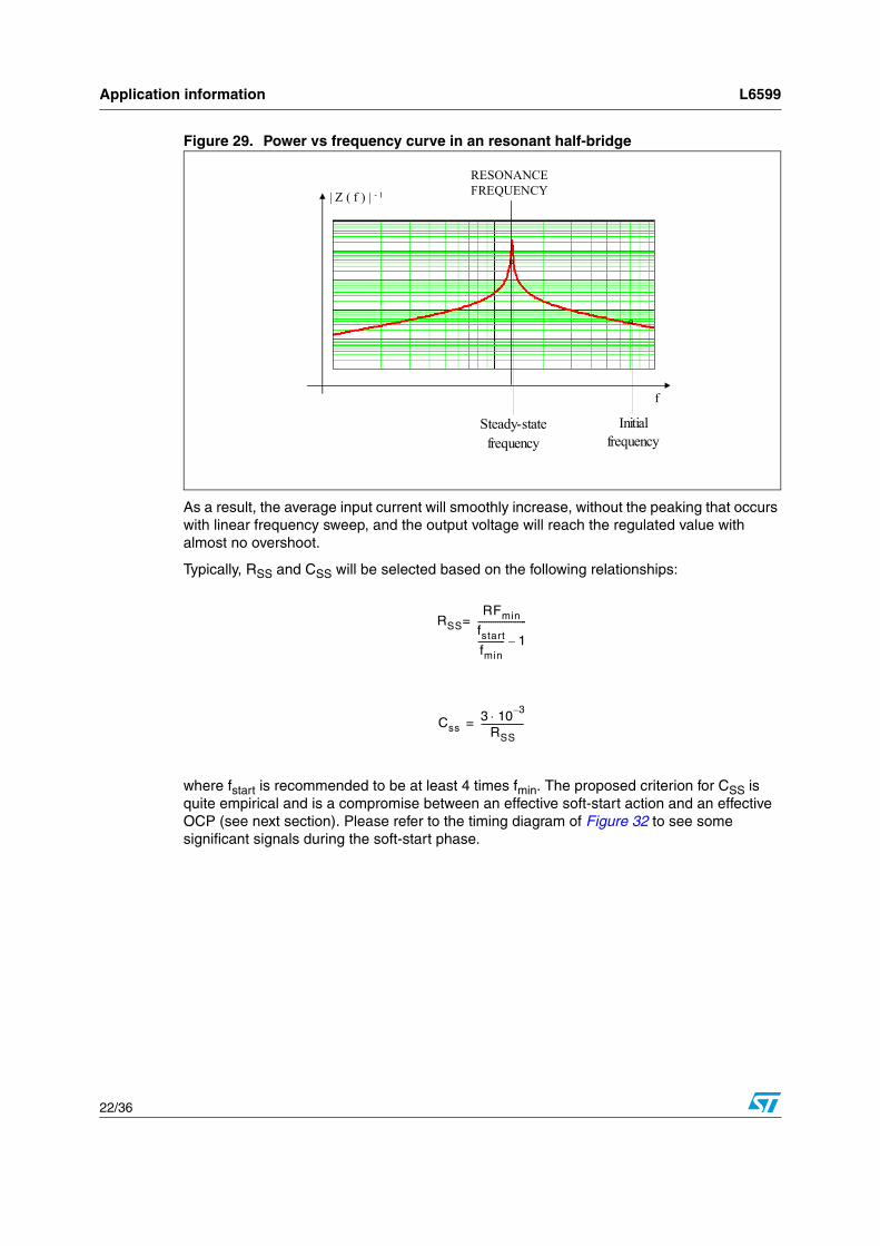
During this frequency sweep phase the operating frequency will decay following the exponential charge of CSS, that is, initially it will change relatively quickly but the rate of change will get slower and slower. This counteracts the non-linear frequency dependence of the tank circuit that makes converter's power capability change little as frequency is away from resonance and change very quickly as frequency approaches resonance frequency (see Figure 29).
Figure 28. Soft-start circuit
fstart1
3 CF R Fmin RSS||( )( )⋅ ⋅---------------------------------------------------------------=
L6599Css
4
1
RFmin
RFmin RSS
CSS
| Z ( f ) |
Application information L6599
22/36
Figure 29. Power vs frequency curve in an resonant half-bridge
As a result, the average input current will smoothly increase, without the peaking that occurs with linear frequency sweep, and the output voltage will reach the regulated value with almost no overshoot.
Typically, RSS and CSS will be selected based on the following relationships:
where fstart is recommended to be at least 4 times fmin. The proposed criterion for CSS is quite empirical and is a compromise between an effective soft-start action and an effective OCP (see next section). Please refer to the timing diagram of Figure 32 to see some significant signals during the soft-start phase.
RESONANCE FREQUENCY
f
| Z ( f ) | - 1
Initialfrequency
Steady-statefrequency
RSSRFmin
fstart
fmin------------ 1–
----------------------=
Css3 10 3–⋅
RSS-------------------=
L6599 Application information
23/36
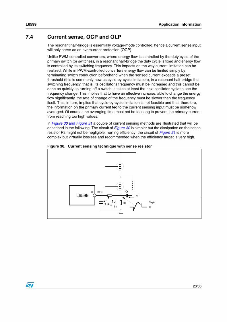
7.4 Current sense, OCP and OLPThe resonant half-bridge is essentially voltage-mode controlled; hence a current sense input will only serve as an overcurrent protection (OCP).
Unlike PWM-controlled converters, where energy flow is controlled by the duty cycle of the primary switch (or switches), in a resonant half-bridge the duty cycle is fixed and energy flow is controlled by its switching frequency. This impacts on the way current limitation can be realized. While in PWM-controlled converters energy flow can be limited simply by terminating switch conduction beforehand when the sensed current exceeds a preset threshold (this is commonly now as cycle-by-cycle limitation), in a resonant half-bridge the switching frequency, that is, its oscillator's frequency must be increased and this cannot be done as quickly as turning off a switch: it takes at least the next oscillator cycle to see the frequency change. This implies that to have an effective increase, able to change the energy flow significantly, the rate of change of the frequency must be slower than the frequency itself. This, in turn, implies that cycle-by-cycle limitation is not feasible and that, therefore, the information on the primary current fed to the current sensing input must be somehow averaged. Of course, the averaging time must not be too long to prevent the primary current from reaching too high values.
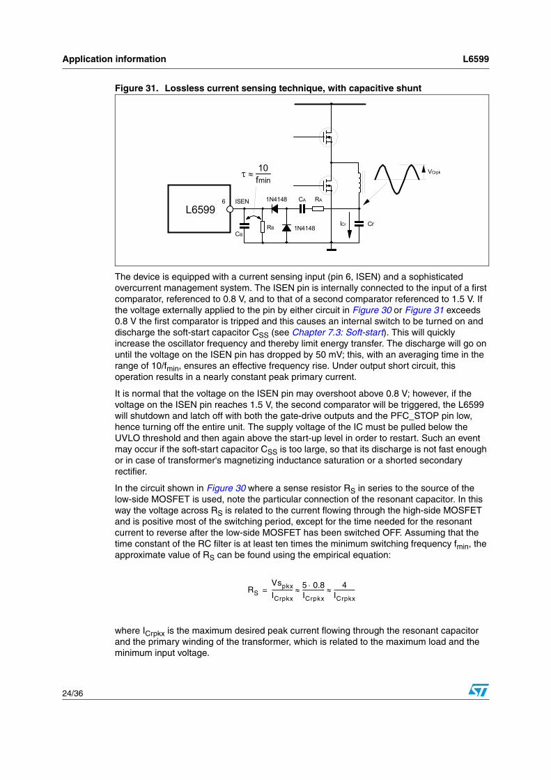
In Figure 30 and Figure 31 a couple of current sensing methods are illustrated that will be described in the following. The circuit of Figure 30 is simpler but the dissipation on the sense resistor Rs might not be negligible, hurting efficiency; the circuit of Figure 31 is more complex but virtually lossless and recommended when the efficiency target is very high.
Figure 30. Current sensing technique with sense resistor
L65996 ISEN
τ ≈ 10fmin
Rs0
Cr
Vspk
ICr L65996
Application information L6599
24/36
Figure 31. Lossless current sensing technique, with capacitive shunt
The device is equipped with a current sensing input (pin 6, ISEN) and a sophisticated overcurrent management system. The ISEN pin is internally connected to the input of a first comparator, referenced to 0.8 V, and to that of a second comparator referenced to 1.5 V. If the voltage externally applied to the pin by either circuit in Figure 30 or Figure 31 exceeds 0.8 V the first comparator is tripped and this causes an internal switch to be turned on and discharge the soft-start capacitor CSS (see Chapter 7.3: Soft-start). This will quickly increase the oscillator frequency and thereby limit energy transfer. The discharge will go on until the voltage on the ISEN pin has dropped by 50 mV; this, with an averaging time in the range of 10/fmin, ensures an effective frequency rise. Under output short circuit, this operation results in a nearly constant peak primary current.
It is normal that the voltage on the ISEN pin may overshoot above 0.8 V; however, if the voltage on the ISEN pin reaches 1.5 V, the second comparator will be triggered, the L6599 will shutdown and latch off with both the gate-drive outputs and the PFC_STOP pin low, hence turning off the entire unit. The supply voltage of the IC must be pulled below the UVLO threshold and then again above the start-up level in order to restart. Such an event may occur if the soft-start capacitor CSS is too large, so that its discharge is not fast enough or in case of transformer's magnetizing inductance saturation or a shorted secondary rectifier.
In the circuit shown in Figure 30 where a sense resistor RS in series to the source of the low-side MOSFET is used, note the particular connection of the resonant capacitor. In this way the voltage across RS is related to the current flowing through the high-side MOSFET and is positive most of the switching period, except for the time needed for the resonant current to reverse after the low-side MOSFET has been switched OFF. Assuming that the time constant of the RC filter is at least ten times the minimum switching frequency fmin, the approximate value of RS can be found using the empirical equation:
where ICrpkx is the maximum desired peak current flowing through the resonant capacitor and the primary winding of the transformer, which is related to the maximum load and the minimum input voltage.
pk
L65996 ISEN
Cr
RA
RB 1N4148CB
CA1N4148
τ ≈ 10fmin
VCrpk
ICr
RS
Vspkx
ICrpkx--------------- 5 0.8⋅
ICrpkx---------------- 4
ICrpkx---------------≈ ≈=
L6599 Application information
25/36
The circuit shown in Figure 31 can be operated in two different ways. If the resistor RA in series to CA is small (not above some hundred Ω, just to limit current spiking) the circuit operates like a capacitive current divider; CA will be typically selected equal to CR/100 or less and will be a low-loss type, the sense resistor RB will be selected as:
and CB will be such that RB·CB is in the range of 10 /fmin.
If the resistor RA in series to CA is not small (in this case it will be typically selected in the ten kΩ ), the circuit operates like a divider of the ripple voltage across the resonant capacitor Cr, which, in turn, is related to its current through the reactance of Cr. Again, CA will be typically selected equal to CR/100 or less, this time not necessarily a low-loss type, while RB (provided it is << RA) according to:
where the reactance of CA (XCA) and CR (XCr) should be calculated at the frequency where ICrpk = ICrpkx. Again, CB will be such that RB·CB is in the range of 10 /fmin.
Whichever circuit one is going to use, the calculated values of RS or RB should be considered just a first cut value that needs to be adjusted after experimental verification.
OCP is effective in limiting primary-to-secondary energy flow in case of an overload or an output short circuit, but the output current through the secondary winding and rectifiers under these conditions might be so high to endanger converter's safety if continuously flowing. To prevent any damage during these conditions it is customary to force converter's intermittent operation, in order to bring the average output current to values such that the thermal stress for the transformer and the rectifiers can be easily handled.
With the L6599 the designer can program externally the maximum time TSH that the converter is allowed to run overloaded or under short circuit conditions. Overloads or short circuits lasting less than TSH will not cause any other action, hence providing the system with immunity to short duration phenomena. If, instead, TSH is exceeded an overload protection (OLP) procedure is activated that shuts down the device and, in case of continuous overload/short circuit, results in continuous intermittent operation with a user-defined duty cycle.
RB0.8π
ICrpkx--------------- 1
Cr
CA-------+⎝ ⎠
⎛ ⎞=
RB0.8π
ICrpkx---------------
RA2 XCA
2+
XCr
----------------------------⋅=
Application information L6599
26/36
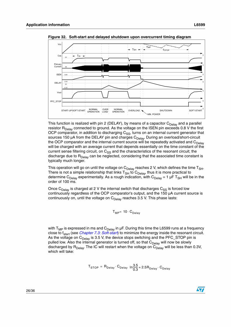
Figure 32. Soft-start and delayed shutdown upon overcurrent timing diagram
This function is realized with pin 2 (DELAY), by means of a capacitor CDelay and a parallel resistor RDelay connected to ground. As the voltage on the ISEN pin exceeds 0.8 V the first OCP comparator, in addition to discharging CSS, turns on an internal current generator that sources 150 µA from the DELAY pin and charges CDelay. During an overload/short-circuit the OCP comparator and the internal current source will be repeatedly activated and CDelay will be charged with an average current that depends essentially on the time constant of the current sense filtering circuit, on CSS and the characteristics of the resonant circuit; the discharge due to RDelay can be neglected, considering that the associated time constant is typically much longer.
This operation will go on until the voltage on CDelay reaches 2 V, which defines the time TSH. There is not a simple relationship that links TSH to CDelay, thus it is more practical to determine CDelay experimentally. As a rough indication, with CDelay = 1 µF TSH will be in the order of 100 ms.
Once CDelay is charged at 2 V the internal switch that discharges CSS is forced low continuously regardless of the OCP comparator's output, and the 150 µA current source is continuously on, until the voltage on CDelay reaches 3.5 V. This phase lasts:
with TMP is expressed in ms and CDelay in µF. During this time the L6599 runs at a frequency close to fstart (see Chapter 7.3: Soft-start) to minimize the energy inside the resonant circuit. As the voltage on CDelay is 3.5 V, the device stops switching and the PFC_STOP pin is pulled low. Also the internal generator is turned off, so that CDelay will now be slowly discharged by RDelay. The IC will restart when the voltage on CDelay will be less than 0.3V, which will take:
t
Vcc
Css
t
tDELAY
START-UP OVERLOAD OVERLOAD
t
PrimaryCurrent
NORMALOPERATION
NORMALOPERATION SHUTDOWN
2V
Voutt
0A
SOFT-START SOFT-START
2V
3.5V
0.3V
MIN. POWER
t
PFC_STOP
ISEN t0.8V
TSH TSTOP TMP
Tss
TMP 10 CDelay⋅=
TSTOP RDelay CDelay⋅= ln3.50.3-------- 2.5RDelay≈ CDelay⋅
L6599 Application information
27/36
The timing diagram of Figure 32 shows this operation.
Note that if during TSTOP the supply voltage of the L6599 (Vcc) falls below the UVLO threshold the IC keeps memory of the event and will not restart immediately after VCC exceeds the start-up threshold if V(DELAY) is still higher than 0.3 V. Also the PFC_STOP pin will stay low as long as V(DELAY) is greater than 0.3 V. Note also that in case there is an overload lasting less than TSH, the value of TSH for the next overload will be lower if they are close to one another.
7.5 Latched shutdownThe device is equipped with a comparator having the non-inverting input externally available at pin 8 (DIS) and with the inverting input internally referenced to 1.85 ‘V. As the voltage on the pin exceeds the internal threshold, the IC is immediately shut down and its consumption reduced at a low value. The information is latched and it is necessary to let the voltage on the Vcc pin go below the UVLO threshold to reset the latch and restart the IC.
This function is useful to implement a latched overtemperature protection very easily by biasing the pin with a divider from an external reference voltage, where the upper resistor is an NTC physically located close to a heating element like the MOSFET, or the secondary diode or the transformer.
An OVP can be implemented as well, e.g. by sensing the output voltage and transferring an overvoltage condition via an optocoupler.
7.6 Line sensing functionThis function basically stops the IC as the input voltage to the converter falls below the specified range and lets it restart as the voltage goes back within the range. The sensed voltage can be either the rectified and filtered mains voltage, in which case the function will act as a brownout protection, or, in systems with a PFC pre-regulator front-end, the output voltage of the PFC stage, in which case the function will serve as power-on and power-off sequencing.
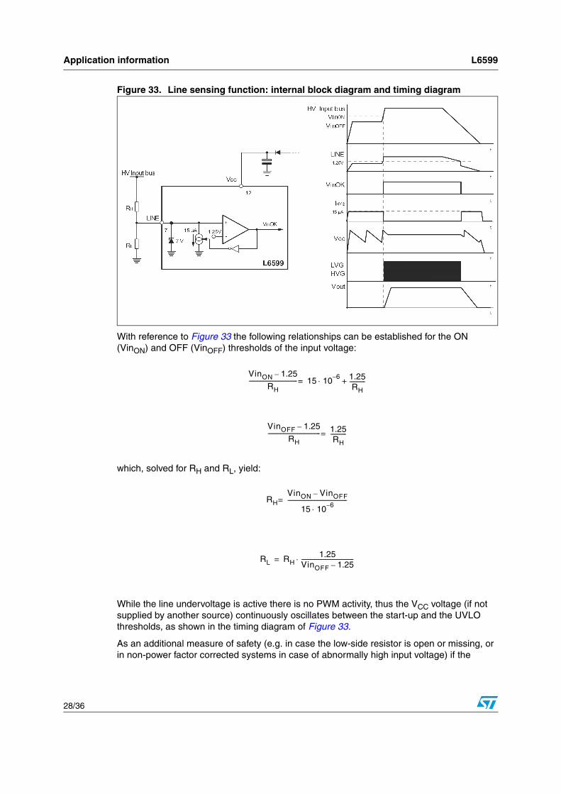
L6599 shutdown upon input undervoltage is accomplished by means of an internal comparator, as shown in the block diagram of Figure 33, whose non-inverting input is available at pin 7 (LINE). The comparator is internally referenced to 1.25 V and disables the IC if the voltage applied on the LINE pin is below the internal reference. Under these conditions the soft-start is discharged, the PFC_STOP pin is open and the consumption of the IC is reduced. PWM operation is re-enabled as the voltage on the pin is above the reference. The comparator is provided with current hysteresis instead of a more usual voltage hysteresis: an internal 1 µA current sink is ON as long as the voltage on the LINE pin is below the reference and is OFF if the voltage is above the reference.
This approach provides an additional degree of freedom: it is possible to set the ON threshold and the OFF threshold separately by properly choosing the resistors of the external divider (see below). With voltage hysteresis, instead, fixing one threshold automatically fixes the other one depending on the built-in hysteresis of the comparator.
Application information L6599
28/36
Figure 33. Line sensing function: internal block diagram and timing diagram
With reference to Figure 33 the following relationships can be established for the ON (VinON) and OFF (VinOFF) thresholds of the input voltage:
which, solved for RH and RL, yield:
While the line undervoltage is active there is no PWM activity, thus the VCC voltage (if not supplied by another source) continuously oscillates between the start-up and the UVLO thresholds, as shown in the timing diagram of Figure 33.
As an additional measure of safety (e.g. in case the low-side resistor is open or missing, or in non-power factor corrected systems in case of abnormally high input voltage) if the
VinON 1.25–
RH---------------------------------- 15 10 6– 1.25
RH-----------+⋅=
VinOFF 1.25–
RH------------------------------------- 1.25
RH-----------=
RHVinON VinOFF–
15 10 6–⋅------------------------------------------=
RL RH1.25
VinOFF 1.25–-------------------------------------⋅=
L6599 Application information
29/36
voltage on the pin exceeds 7 V the device is shutdown. If its supply voltage is always above the UVLO threshold, the IC will restart as the voltage falls below 7 V.
The LINE pin, while the device is operating, is a high impedance input connected to high value resistors, thus it is prone to pick up noise, which might alter the OFF threshold or give origin to undesired switch-off of the IC during ESD tests. It is possible to bypass the pin to ground with a small film capacitor (e.g. 1-10 nF) to prevent any malfunctioning of this kind. If the function is not used the pin has to be connected to a voltage greater than 1.25 V but lower than 6V (worst-case value of the 7 V threshold).
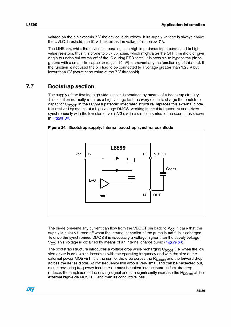
7.7 Bootstrap sectionThe supply of the floating high-side section is obtained by means of a bootstrap circuitry. This solution normally requires a high voltage fast recovery diode to charge the bootstrap capacitor CBOOT. In the L6599 a patented integrated structure, replaces this external diode. It is realized by means of a high voltage DMOS, working in the third quadrant and driven synchronously with the low side driver (LVG), with a diode in series to the source, as shown in Figure 34.
Figure 34. Bootstrap supply: internal bootstrap synchronous diode
The diode prevents any current can flow from the VBOOT pin back to VCC in case that the supply is quickly turned off when the internal capacitor of the pump is not fully discharged. To drive the synchronous DMOS it is necessary a voltage higher than the supply voltage VCC. This voltage is obtained by means of an internal charge pump (Figure 34).
The bootstrap structure introduces a voltage drop while recharging CBOOT (i.e. when the low side driver is on), which increases with the operating frequency and with the size of the external power MOSFET. It is the sum of the drop across the RDS(on) and the forward drop across the series diode. At low frequency this drop is very small and can be neglected but, as the operating frequency increases, it must be taken into account. In fact, the drop reduces the amplitude of the driving signal and can significantly increase the RDS(on) of the external high-side MOSFET and then its conductive loss.
L6599
14 OUT
16 VBOOTVcc 12
LVG
CBOOT
Application information L6599
30/36
This concern applies to converters designed with a high resonance frequency (indicatively, > 150 kHz), so that they run at high frequency also at full load. Otherwise, the converter will run at high frequency only at light load, where the current flowing in the MOSFETs of the half-bridge leg is lower, so that, generally, an RDS(on) rise is not an issue. However, it is wise to check this point anyway and the following equation is useful to compute the drop on the bootstrap driver:
where Qg is the gate charge of the external power MOS, RDS(on) is the on-resistance of the bootstrap DMOS (150, typ.) and Tcharge is the ON-time of the bootstrap driver, which equals about half the switching period minus the dead time TD. For example, using a MOSFET with a total gate charge of 30 nC, the drop on the bootstrap driver is about 3 V at a switching frequency of 200 kHz:
If a significant drop on the bootstrap driver is an issue, an external ultra-fast diode can be used, thus saving the drop on the RDS(on) of the internal DMOS.
VDrop ICh earg r DS( )ON VF
Qg
TCh earg--------------------R DS( )ON VF+=+=
VDrop30 10 9–⋅
2.5 10 6– 0.3 10 6–⋅–⋅-------------------------------------------------------150 0.6 2.7V=+=
L6599 Application information
31/36
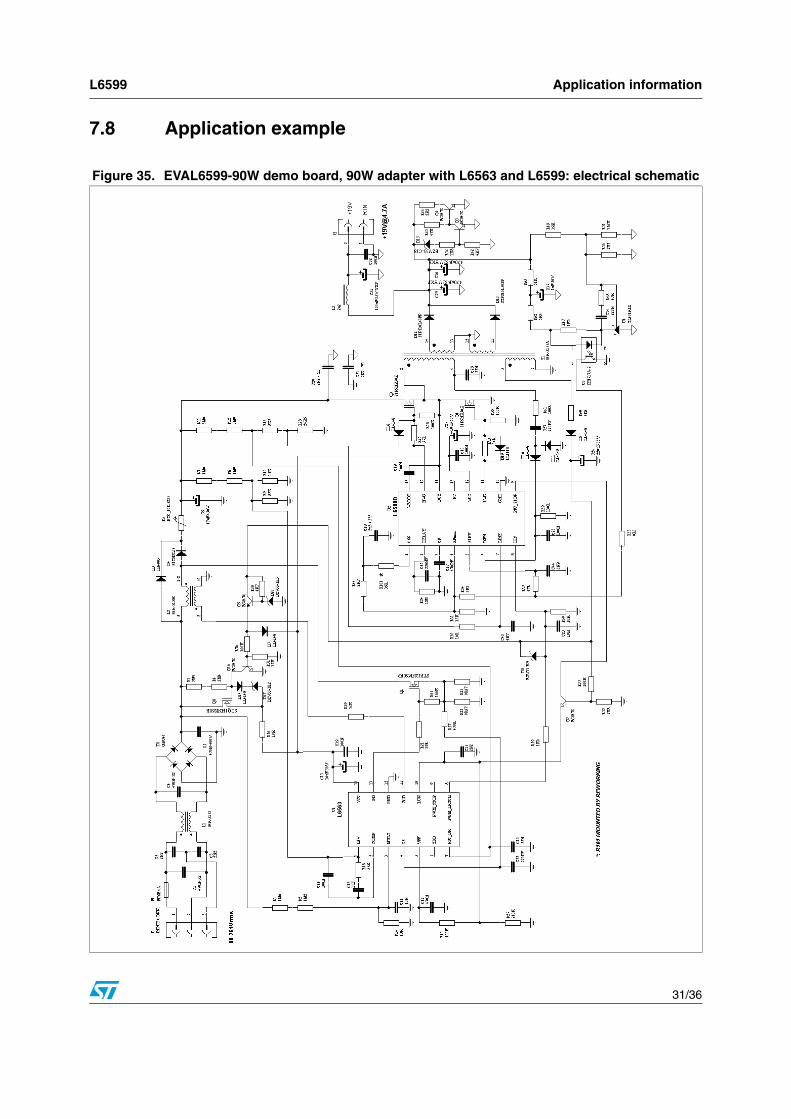
7.8 Application example
Figure 35. EVAL6599-90W demo board, 90W adapter with L6563 and L6599: electrical schematic
Application information L6599
32/36
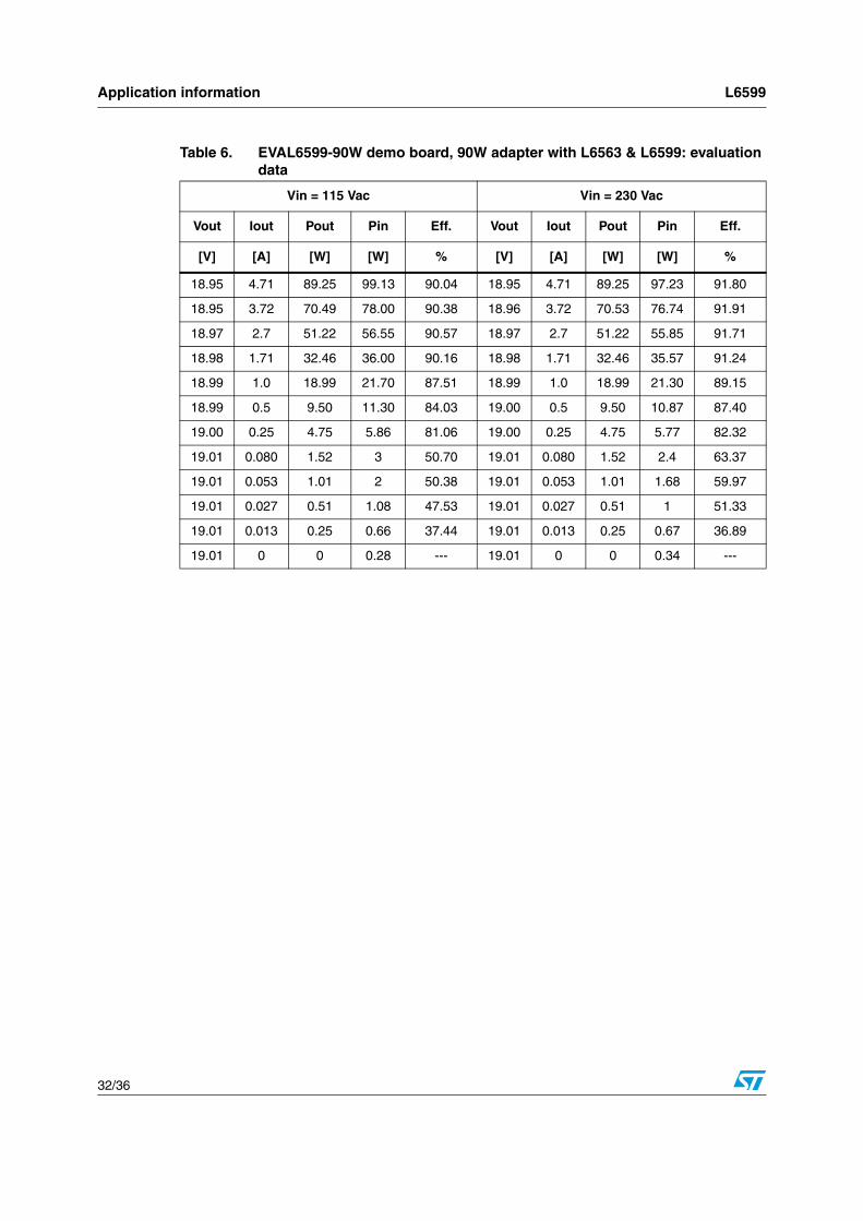
Table 6. EVAL6599-90W demo board, 90W adapter with L6563 & L6599: evaluation data
Vin = 115 Vac Vin = 230 Vac
Vout Iout Pout Pin Eff. Vout Iout Pout Pin Eff.
[V] [A] [W] [W] % [V] [A] [W] [W] %
18.95 4.71 89.25 99.13 90.04 18.95 4.71 89.25 97.23 91.80
18.95 3.72 70.49 78.00 90.38 18.96 3.72 70.53 76.74 91.91
18.97 2.7 51.22 56.55 90.57 18.97 2.7 51.22 55.85 91.71
18.98 1.71 32.46 36.00 90.16 18.98 1.71 32.46 35.57 91.24
18.99 1.0 18.99 21.70 87.51 18.99 1.0 18.99 21.30 89.15
18.99 0.5 9.50 11.30 84.03 19.00 0.5 9.50 10.87 87.40
19.00 0.25 4.75 5.86 81.06 19.00 0.25 4.75 5.77 82.32
19.01 0.080 1.52 3 50.70 19.01 0.080 1.52 2.4 63.37
19.01 0.053 1.01 2 50.38 19.01 0.053 1.01 1.68 59.97
19.01 0.027 0.51 1.08 47.53 19.01 0.027 0.51 1 51.33
19.01 0.013 0.25 0.66 37.44 19.01 0.013 0.25 0.67 36.89
19.01 0 0 0.28 --- 19.01 0 0 0.34 ---
L6599 Package mechanical data
33/36
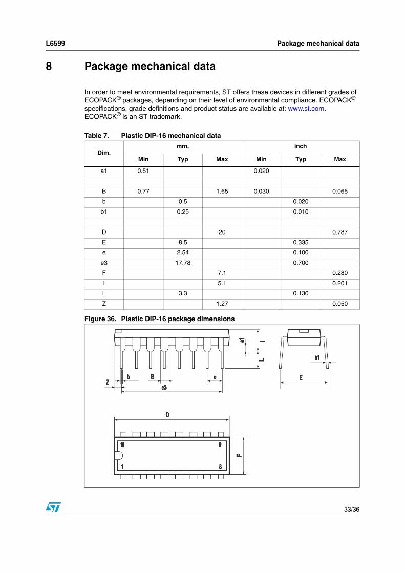
8 Package mechanical data
In order to meet environmental requirements, ST offers these devices in different grades of ECOPACK® packages, depending on their level of environmental compliance. ECOPACK® specifications, grade definitions and product status are available at: www.st.com. ECOPACK® is an ST trademark.
Table 7. Plastic DIP-16 mechanical data
Dim. mm. inch
Min Typ Max Min Typ Max
a1 0.51 0.020
B 0.77 1.65 0.030 0.065
b 0.5 0.020
b1 0.25 0.010
D 20 0.787
E 8.5 0.335
e 2.54 0.100
e3 17.78 0.700
F 7.1 0.280
I 5.1 0.201
L 3.3 0.130
Z 1.27 0.050
Figure 36. Plastic DIP-16 package dimensions
Package mechanical data L6599
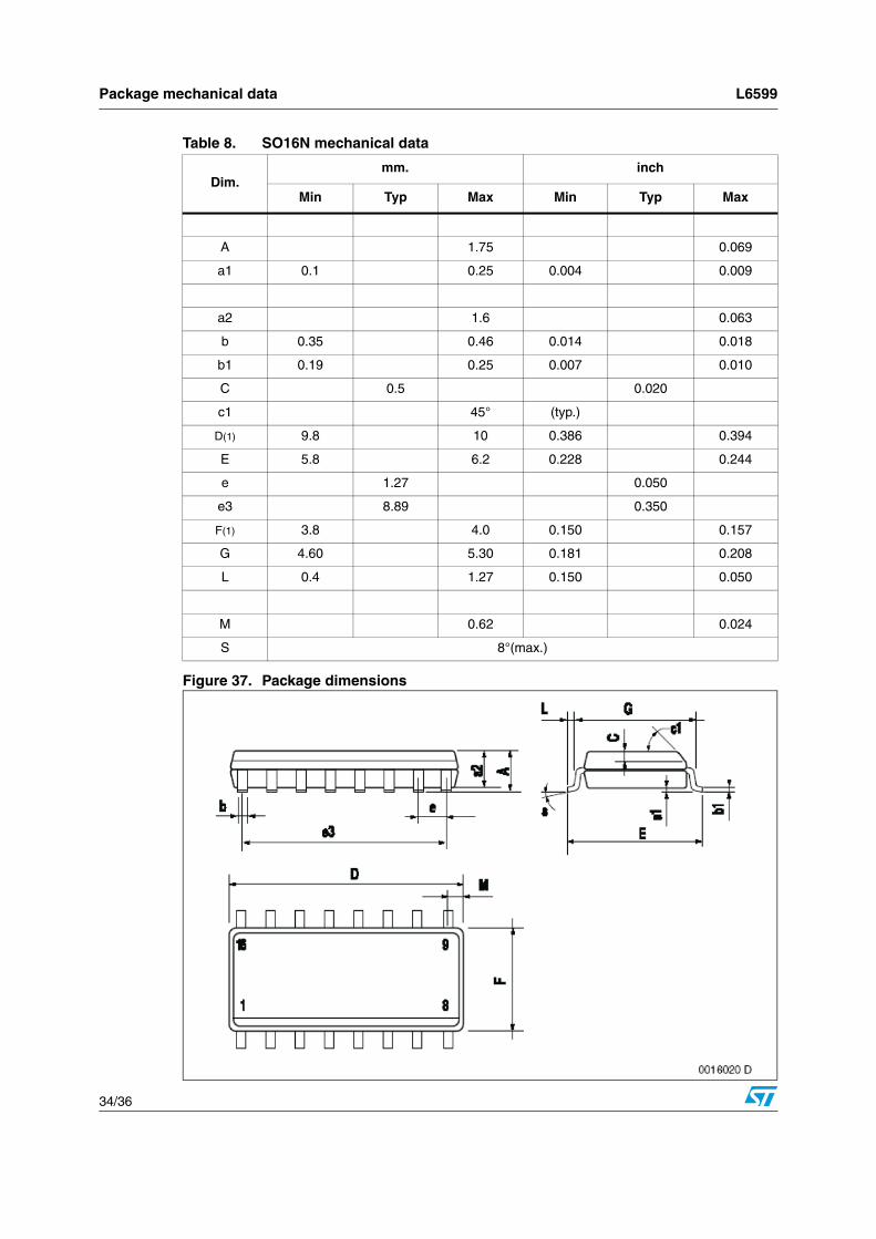
34/36
Figure 37. Package dimensions
Table 8. SO16N mechanical data
Dim. mm. inch
Min Typ Max Min Typ Max
A 1.75 0.069
a1 0.1 0.25 0.004 0.009
a2 1.6 0.063
b 0.35 0.46 0.014 0.018
b1 0.19 0.25 0.007 0.010
C 0.5 0.020
c1 45° (typ.)
D(1) 9.8 10 0.386 0.394
E 5.8 6.2 0.228 0.244
e 1.27 0.050
e3 8.89 0.350
F(1) 3.8 4.0 0.150 0.157
G 4.60 5.30 0.181 0.208
L 0.4 1.27 0.150 0.050
M 0.62 0.024
S 8°(max.)
L6599 Revision history
35/36
9 Revision history
Table 9. Document revision history
Date Revision Changes
15-May-2006 1 Initial release
18-Jul-2006 2 Typo in cover page
11-Feb-2009 3Not recommended for new designs, the device has been replaced by L6599A
L6599
36/36
Please Read Carefully:
Information in this document is provided solely in connection with ST products. STMicroelectronics NV and its subsidiaries (“ST”) reserve theright to make changes, corrections, modifications or improvements, to this document, and the products and services described herein at anytime, without notice.
All ST products are sold pursuant to ST’s terms and conditions of sale.
Purchasers are solely responsible for the choice, selection and use of the ST products and services described herein, and ST assumes noliability whatsoever relating to the choice, selection or use of the ST products and services described herein.
No license, express or implied, by estoppel or otherwise, to any intellectual property rights is granted under this document. If any part of thisdocument refers to any third party products or services it shall not be deemed a license grant by ST for the use of such third party productsor services, or any intellectual property contained therein or considered as a warranty covering the use in any manner whatsoever of suchthird party products or services or any intellectual property contained therein.
UNLESS OTHERWISE SET FORTH IN ST’S TERMS AND CONDITIONS OF SALE ST DISCLAIMS ANY EXPRESS OR IMPLIEDWARRANTY WITH RESPECT TO THE USE AND/OR SALE OF ST PRODUCTS INCLUDING WITHOUT LIMITATION IMPLIEDWARRANTIES OF MERCHANTABILITY, FITNESS FOR A PARTICULAR PURPOSE (AND THEIR EQUIVALENTS UNDER THE LAWSOF ANY JURISDICTION), OR INFRINGEMENT OF ANY PATENT, COPYRIGHT OR OTHER INTELLECTUAL PROPERTY RIGHT.
UNLESS EXPRESSLY APPROVED IN WRITING BY AN AUTHORIZED ST REPRESENTATIVE, ST PRODUCTS ARE NOTRECOMMENDED, AUTHORIZED OR WARRANTED FOR USE IN MILITARY, AIR CRAFT, SPACE, LIFE SAVING, OR LIFE SUSTAININGAPPLICATIONS, NOR IN PRODUCTS OR SYSTEMS WHERE FAILURE OR MALFUNCTION MAY RESULT IN PERSONAL INJURY,DEATH, OR SEVERE PROPERTY OR ENVIRONMENTAL DAMAGE. ST PRODUCTS WHICH ARE NOT SPECIFIED AS "AUTOMOTIVEGRADE" MAY ONLY BE USED IN AUTOMOTIVE APPLICATIONS AT USER’S OWN RISK.
Resale of ST products with provisions different from the statements and/or technical features set forth in this document shall immediately voidany warranty granted by ST for the ST product or service described herein and shall not create or extend in any manner whatsoever, anyliability of ST.
ST and the ST logo are trademarks or registered trademarks of ST in various countries.
Information in this document supersedes and replaces all information previously supplied.
The ST logo is a registered trademark of STMicroelectronics. All other names are the property of their respective owners.
© 2009 STMicroelectronics - All rights reserved
STMicroelectronics group of companies
Australia - Belgium - Brazil - Canada - China - Czech Republic - Finland - France - Germany - Hong Kong - India - Israel - Italy - Japan - Malaysia - Malta - Morocco - Singapore - Spain - Sweden - Switzerland - United Kingdom - United States of America
www.st.com