high speed characteristics of vcsels - welcome to … speed... · high speed characteristics of...
TRANSCRIPT

High Speed Characteristics of VCSELs
Jim Tatum*, David Smith, Jim Guenter and Ralph Johnson
Honeywell’s MICRO SWITCH Division, 830 East Arapaho Rd., Richardson, TX, 75081
ABSTRACTThe high speed characteristics of Vertical Cavity Surface Emitting Lasers (VCSELs) for use in modern high
bandwidth fiber optic networks is presented. An equivalent circuit model based on microwave network analyzer S 11
measurements is developed. The dynamic operation of multi-transverse mode VCSELs is also investigated. Experimentally,a laser with two orthogonally polarized modes is examined. We show that each of the transverse laser modes may havesignificantly different rise and fall times. A multimode rate equation model is used to predict the exact pulseshape for eachmode. The laser gain is saturated by the total optical intensity, and the sum of the modal powers is shown to have a constantrise and fall time. The system performance in terms of the bit error rate is also investigated. We demonstrate that selectiveattenuation of the optical modes can lead to an increase in the bit error rate due to polarization partitioning noise.Keywords: VCSEL, High Speed Modulation, Fiber Optic Networks
1. INTRODUCTION
The Vertical Cavity Surface Emitting Laser (VCSEL) is emergin g as the light source of choice for modern highspeed, short wavelength communication systems. The inherent low cost of manufacture [1], enhanced reliability [2], non-astigmatic and circularly symmetric optical output are among the advantages of VCSELs over traditional edge emittinglasers. However much of the development and characterization performed on edge emitting devices must be reexamined foruse with the VCSEL. For edge emitting lasers typically used in short wavelength telecommunication applications, there hasbeen a vast amount of work done to ensure stable single transverse mode emission, and in some cases single longitudinalmode operation. Single transverse mode operation increases the efficiency of coupling light into a fiber optic cable, and thelow longitudinal mode count significantly reduces chromatic dispersion in the fiber. In VCSEL emission, the output istypically multi-transverse mode and single longitudinal mode. The total spectral width of the emission is generally less than5 Angstroms, which ensures a low coherence source, but not at the expense of chromatic dispersion. The circularlysymmetric and non astigmatic emission of the VCSEL, even in multi-transverse modes, typically has a beam divergenceangle less than 12 ° FWHM (NA=0.12). This easily couples into high NA (0.275) multimode (62.5/125 µm) graded indexfiber generally found in LAN backbones. The narrow beam emission is set by the coupling of the mode to the Bragg grating,and for high contrast gratings, the mode size is reduced and the emission angle is increased. Finally, the surface emittingstructure and small mode size enables production of highly uniform and densely packed lasers, with minimal crosstalk, foruse in parallel optical links.
The lasers used in this work were grown by low pressure MOCVD, and designed to emit at 850nm [2,3]. Thestructure is shown schematically in Fig. 1. The p-mirror stack consists of 20.5 periods of alternating layers ofAlAs/Al 0.15Ga0.85As. The active region contains three GaAs quantum wells surrounded by Al 0.25Ga0.75As spacers, and thecavity is spaced to form a single wavelength cavity with Al 0.6Ga0.4As. The n-mirror consists of 22.5 periods ofAlAs/Al 0.15Ga0.85As pairs grown on an n-type GaAs substrate. Current confinement was achieved by proton implantation.The VCSEL is intended for commercial use and has an inner diameter of 20 µm and a top metal aperture of 15µm. Thisprovides the best balance of threshold current, modulation bandwidth, series resistance and spectral width. Typical forwardvoltage and light output versus current relationship for ambient temperatures of 10,40 and 70 °C are shown in Fig. 2. Thelaser threshold current is stable within 1mA over approximately 80 °C temperature variation. This allows VCSELs to beused in an open loop driving circuit, significantly reducing the cost. The forward operating voltage is typically 1.8V with aseries resistance of 20 Ohms, enabling the VCSEL to be driven directly with low voltage sources and PECL/ECL logic.Typical slope efficiencies are 0.2mW/mA.
* Email: [email protected]; Phone: 972-470-4572; Web: http://www.sensing.honeywell.com

2. EQUIVALENT CIRCUIT PARAMETERS.
The equivalent lumped circuit model of a VCSEL is of great practical utility to design interface drive circuits forhigh speed modulation. To measure the impedance of a VCSEL, packaging parasitics were minimized by uising silverepoxy to mount a VCSEL on a copper circuit board. Electrical contact was made via a wire bond attached to a 50 ohmcustom ceramic stripline. The stripline was electrically contacted through a high speed microwave probe. The stripline and
the probe have a bandwidth in excess of 20Ghz. A networkanalyzer, calibrated to the end of the microstrip line by use of anidentical ceramic standard, was used to measure the reflection (S 11)coefficient as a function of frequency and dc bias current. To ensurethe VCSEL was being modulated in the small signal regime, theinput electrical power was kept under -40dBm. The circuit modelappropriate for subthreshold bias currents is shown in Fig. 3. Thecomponents that make up the equivalent circuit include aninductance L b due to the bond wire, a capacitance Cp from theVCSEL chip, and a resistance R s arising from the metal contactsand the resistance of the Bragg mirror stack. The p-n junction ismodeled by a capacitance C j and a resistance R j in parallel. The
0.0
0.5
1.0
1.5
2.0
2.5
3.0
3.5
0 5 10 15Current (mA)
Pow
er (m
w)
1.0
1.5
2.0
Forw
ard
Vol
tage
(V)
10°C40°C70°C
Figure 2 Typical LIV curves for 10, 40 and 70C.
p-Contactp-Mirror StackProton ImplantActive Region
n-Mirror Stack
GaAs Substrate
Figure 1 Schematic of a VCSEL.
Figure 3 VCSEL Equivalent circuit
0
10
20
30
40
50
60
70
80
0 1 10 100 1000 10000Frequency (MHz)
Mag
nitu
de Z
(Ohm
s)
-25
-20
-15
-10
-5
0
5
Pha
se Z
(Deg
rees
)
Figure 4 Measured and calculated VCSEL impedance
0
0.5
1
1.5
2
2.5
3
3.5
4
4.5
5
0 1000 2000 3000 4000Current (uA)
Car
rier L
ifetim
e (n
s)
Figure 5 Measured differential carrier lifetime and fit.

differential carrier lifetime is given by τd=RjCj. The measured VCSEL impedance magnitude and phase, for a bias currentof 1 mA, is shown in Fig. 4 as the solid lines. The fit obtained using our model is indicated as the broken lines in Fig. 4,and the values of the components are L b=0.25nH, Cp=0.8pF, Rs=35Ω, and τd=1.75ns. At low frequencies, the VCSELimpedance is real, and is giving by the sum of R s and Rj. As the frequency increases, the junction capacitance dominates,and the real part of the impedance reduces to R s. Excellent agreement between the VCSEL and its equivalent circuit areobtained over a very large range of operating temperatures and currents, indicating the appropriateness of our model. Figure5 shows the measured differential carrier lifetime calculated from the impedance measurements as described in [4]. This allelectrical technique yields much more accurate results than the commonly used optical techniques, particularly at the lowbias currents associated with VCSEL operation. Accurate carrier lifetime measurements allow for a proper estimation of thethreshold carrier density, which in turn enables estimation of non-radiative recombination processes. The solid line in Fig. 5is a fit to the measured carrier lifetime as a function of the dc bias current. We find the carrier lifetime can be approximatedby:
τ d I≅ +0 033
16 853
..
where I is the injected current in µA, and τd is in ns. The total carrier density in the active region is then found byintegrating the current times the carrier lifetime,
( )n I I dId
I
( ) = ′ ′∫ τ0
yielding a threshold carrier density of 2 ×1018 cm-3. Using traditional optical techniques for carrier density measurements,we would have overestimated the threshold carrier density by about 40%. The simple equivalent circuit model describedhere can be used to quite accurately model the laser impedance for design into communication systems. In addition, thecorrect carrier lifetime measurements allow the optical designer to better understand the mechanics of the laser itself.
3. MULTI-TRANSVERSE MODE OPERATION
In contrast to edge emitting lasers, the orientation of the quantum well active region with respect the Bragg mirrorscauses little polarization selection of the optical output of a VCSEL, and the emission tends to be polarized along the[1 1 0 ] / [110 ] crystallographic axes. This has recently been shown to be caused by a small anisotropy in the elasticlattice tensor [5]. Because of the small anisotropy and a polarization independent gain, the optical modes of a VCSEL areessentially randomly polarized between the two orthogonal [ 110 ] and [1 1 0 ] crystallographic planes. Usingspectroscopically and polarization resolved near field emission, complete families of both Laguerre-Gaussian and Hermite-Gaussian optical modes have been shown to exist in VCSELs [6]. These multiple transverse modes, each with a differentwavelength, help decohere the laser source and thus make it less susceptible to interference effects, such as fiber modalnoise, in communication systems. In Fig. 6 is a plot of the coherence of a VCSEL as a function of the dc current.
0
50
100
150
200
250
300
350
3 4 5 6 7 8 9 10Current (mA)
Coh
eren
ce L
engt
h (m
m)
0
2
4
6
8
10
12
14
16
Effe
ctiv
e Fr
eque
ncy
Wid
th (G
Hz)
Figure 6 Coherence length and effective frequency width of a VCSEL.
0%
10%
20%
30%
40%
50%
60%
70%
80%
90%
100%
0 5 10 15 20DC Current (mA)
Per
cent
Pow
er in
S,P
Pol
ariz
atio
n
Figure 7 Per-cent power in the S and P modes of a VCSEL.
S
P
The coherence was calculated using:
( )[ ]( )
∆νν ν
ν νcoh
S d
S d= ∫
∫
2
2
where S(ν) is the photon density at frequency ν. The optical frequency spectrum at threshold, 3.5mA, was nearly singlefrequency , with a second frequency component appearing at 4.5mA. Typical spectral linewidths were less than 1 Ghz. Athigh bias currents, I>5mA, there are at least 5 independent frequency components evident in the optical spectrum. Thesespectral components were found to tune at 0.065nm/°C and 0.083nm/mA. (This gives a junction temperature rise of1.27°C/mA.) It is important to note the total spectral bandwidth is still less than 5 because the laser is multi-transversemode. The longitudinal mode spacing of the VCSEL is about 40nm. Each of the transverse modes has its wave vectororiented at an angle with respect to the emission direction, and the mode wavelength is defined by the projection of thewave vector onto the optical axis. This projection leads to the small differences in wavelength observed for each transversemode [6,7]. Since each of the transverse modes may be polarized along either the [ 110 ] or the [1 1 0 ] crystallographicplanes, polarizing components in the optical path could severely limit VCSEL performance in an optical system. As anillustration, the per cent power in each of the two orthogonal modes is plotted as a function of the dc bias current in Fig. 7.We have arbitrarily labeled the [ 110 ] direction P, and the [ 1 1 0 ] direction S polarization. As the dc bias current isincreased, the laser polarization is seen to switch between the S and P polarizations. Recently there have been severalattempts by researchers to control the polarization state by introducing anisotropy in either the geometry [8,9] or gain[10,11]. These have met with varying degrees of success, and the impact on device reliability is unknown.
The non-degeneracy of the transverse mode family both spatially and in polarization may lead to a reduction incoherence of the laser, but it also creates some interesting effects when selective modal attenuation mechanisms act on thelaser output field. Selective modal attenuation can be manifested in a number of ways. Polarization selective elements mayoccur in components of the fiber link such as beamsplitters, fused couplers, diffractive lenses etc, each of which maydifferentially attenuate modes depending on their polarization state. In the worst case, they may completely block one modeand pass the other unattenuated. Modes may be selectively spatially attenuated when coupling into fibers or passing throughspatially inhomogeneous optical elements. In particular, overfilled launches into optical fibers or vignetting of beamsthrough aperture stops will tend to select modal fields in the center of the VCSEL and block modes nearer the outerperimeter. In some VCSEL designs modes may even lase under the contact ring, preventing the optical power of thosemodes from leaving the laser.
The effects of selective modal attenuation fall into three broad categories. First there is Bit Error Rate (BER)degradation due to selection induced turn-on jitter [12], secondly there are pulse distortion effects [13], and thirdly there isBER degradation due to selection induced mode partition noise. All of these effects have the same root cause, namely thatthe distribution of power between the lasing modes changes with time even when the total power emitted from the laserappears to have reached steady state saturation [14]. If one of these modes is preferentially selected, the effects of the modecompetition will then become evident as jitter; as mode partition amplitude noise; or as long time constant tailing effects onthe rising edge of the optical pulse.
The effect of polarization selectivity on turn-on delay induced jitter on the rising edge was investigated byKuksenkov et al. [12]. In their case, the polarization selectivity was introduced by breaking the degeneracy of thepolarization eigenmodes in the laser itself. This was accomplished by designing a polarization controlling structure thatcreated enough differential gain between the eigenmodes to allow one of them to become the dominant mode. However, dueto spontaneous emission, there is a finite probability that under transient conditions the laser may start to lase in thesecondary mode and quickly switch to the dominant mode. This would create distortion on the rising edge due to thedifferent gains of the modes, and would be present on some pulses but not on others. This alone would not cause turn-onjitter. However, if an external polarization selective element was also present, then the secondary mode would be blockedentirely and this effect would create turn-on delay jitter in addition to distortion on the rising edge. Even when the totalpower of the modes reaches steady state due to gain saturation of the optical power, the individual modes of the laser maystill be competing with each other for the gain, and may not have reached steady state. Lam et al. showed from a study ofthe multimode rate equations in multi-longitudinal mode quantum well edge emitters that the individual modes may take
more than five times longer to reach steady state than the total power[14]. In the case of a single transverse mode edge emitter, all themodes clearly compete for the same gain, because they occupyessentially the same mode volume. Consequently there is nomechanism where the individual modes can be selectively observedby spatial or polarization means. The long settling times of theindividual modes are typically not observed in edge emitters, and it isonly possible to observe the sum of the power of all the modes. Inmulti-transverse mode VCSELs however, the modes can be spatiallyselected or selected by polarization as described above.
In this section we examine the effect of polarizationselection of modes on pulse rise times by studying the simple case ofa two moded VCSEL where the modes have orthogonal polarizations.The modes have a strong spatial overlap, and thus compete for thesame gain. This allows us to invoke a simple multimode rateequation model, with no spatially dependent terms, to explain theobserved effects.
In order to facilitate testing in fiber networks, a VCSEL wasmounted on a transistor TO46 header and placed on a large thermo-electrically controlled heat sink. A bias tee was employed to allowboth a dc biasing current and an ac modulation current. The laserwas collimated using a 0.12 NA lens, closely matching the VCSELemission. The laser was operated in a multi-transverse mode, and wewere able to separate the orthogonal modes using a polarizer. Inaddition to the fiber network, the light was directed to an averagepower detector; an avalanche photodiode; or a Fabry-Perotinterferometer. To verify the number of modes operating both nearfield images and spectral characteristics were measured.
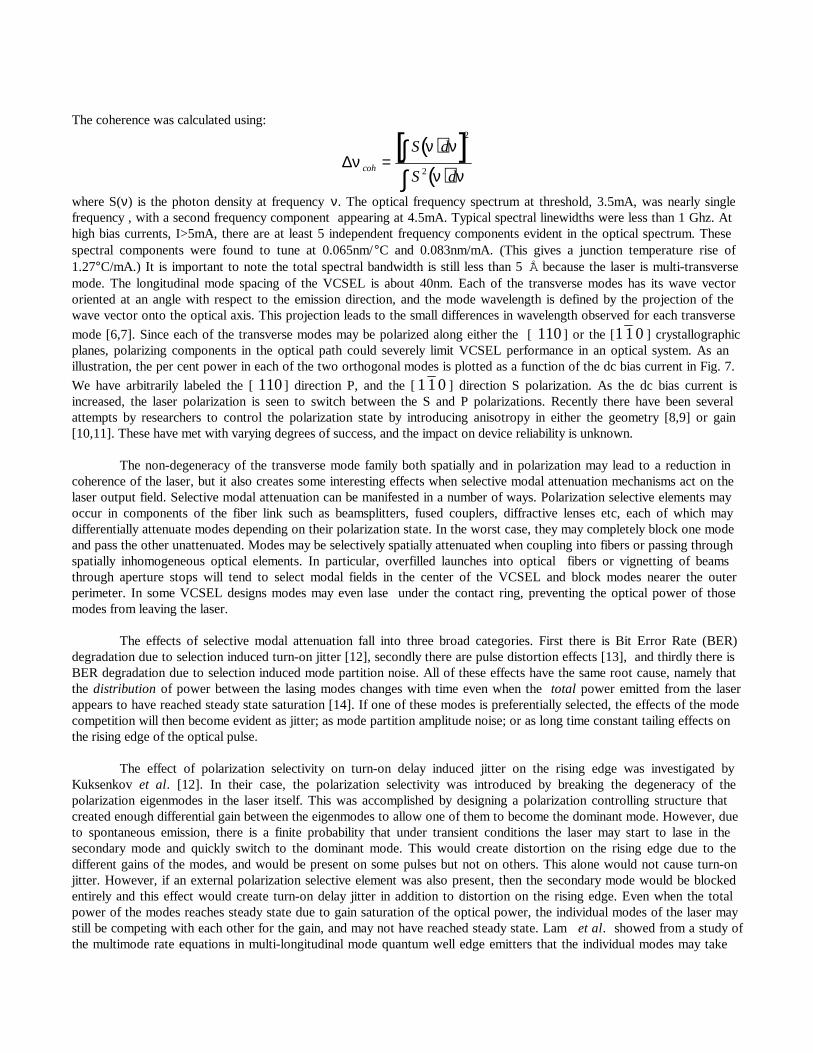
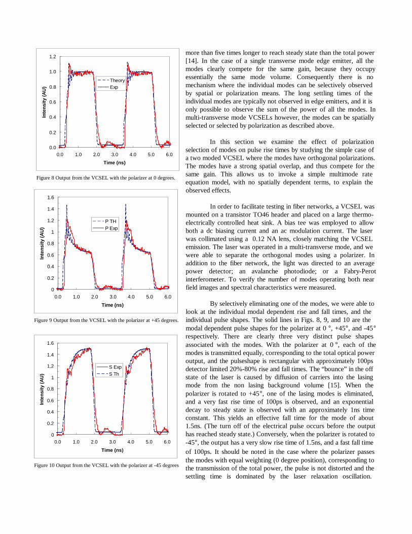
By selectively eliminating one of the modes, we were able tolook at the individual modal dependent rise and fall times, and theindividual pulse shapes. The solid lines in Figs. 8, 9, and 10 are themodal dependent pulse shapes for the polarizer at 0 °, +45°, and -45°respectively. There are clearly three very distinct pulse shapesassociated with the modes. With the polarizer at 0 °, each of themodes is transmitted equally, corresponding to the total optical poweroutput, and the pulseshape is rectangular with approximately 100psdetector limited 20%-80% rise and fall times. The “bounce” in the offstate of the laser is caused by diffusion of carriers into the lasingmode from the non lasing background volume [15]. When thepolarizer is rotated to +45°, one of the lasing modes is eliminated,and a very fast rise time of 100ps is observed, and an exponentialdecay to steady state is observed with an approximately 1ns timeconstant. This yields an effective fall time for the mode of about1.5ns. (The turn off of the electrical pulse occurs before the outputhas reached steady state.) Conversely, when the polarizer is rotated to-45°, the output has a very slow rise time of 1.5ns, and a fast fall timeof 100ps. It should be noted in the case where the polarizer passesthe modes with equal weighting (0 degree position), corresponding tothe transmission of the total power, the pulse is not distorted and thesettling time is dominated by the laser relaxation oscillation.
0.0
0.2
0.4
0.6
0.8
1.0
1.2
0.0 1.0 2.0 3.0 4.0 5.0 6.0
Time (ns)
Inte
nsity
(AU
)
TheoryExp
Figure 8 Output from the VCSEL with the polarizer at 0 degrees.
0
0.2
0.4
0.6
0.8
1
1.2
1.4
1.6
0.0 1.0 2.0 3.0 4.0 5.0 6.0
Time (ns)
Inte
nsity
(AU
)
P THP Exp
Figure 9 Output from the VCSEL with the polarizer at +45 degrees.
0
0.2
0.4
0.6
0.8
1
1.2
1.4
1.6
0.0 1.0 2.0 3.0 4.0 5.0 6.0
Time (ns)
Inte
nsity
(AU
)
S ExpS Th
Figure 10 Output from the VCSEL with the polarizer at -45 degrees

However, when the polarizer is oriented to select only one mode, the pulse shape is severly distorted and the settling time isvery long, and is dominated by mode competition effects rather than the relaxation oscillation. It is intuitively obvious thatif some modes appear to overshoot and then relax back to the steady state value, others will undershoot and have a long risetime. Because the gain saturates as the total intensity, the sum of the two, will exactly compensate each other. In a realworld case where the polarization selection may be partial, the pulse will simply appear to have a slow tail or an overshooton the rising edge. The exact pulseshape will depend on what degree the above compensation has been compromised bydifferentially removing some of the power from the modes. This effect is likely to cause power penalties due to pulsedistortion in a real optical link.
In order to develop an understanding of the possible implications to VCSEL performance in modulationexperiments, we have employed a multimode rate equation model. The rate equations, normalized to their steady statevalues, are given by;
( ) ( )dNdt
N P t N N Ij jj
2
22 2 1
1= − − + −
∑τ
Γ
( )dNdt
N N N N Ij jj
1
21
2
11 2 1
1= − − − −
∑τ
ττ
Γ
( ) ( )dIdt
I N N N N Ij
cj j j j j
j
= − − − − −
∑1
2 1 2 1τβΓ Γ
where N1 is the number of electrons in the valence band, N 2 is the number of electrons in the conduction band, P(t) is theinjected carrier density, and I j is the intensity of the j th mode. All of these values are normalized to the steady statecharacteristics in order to facilitate computer modeling. The time constants in equations (1) - (3) are the spontaneousemission lifetime τ2 (1ns), the hole lifetime τ1 (1ps), and the photon lifetime τc (4ps). The coupling of spontaneousemission to the j th lasing mode is βj, and the mode overlap with the gain region is Γj. It is important to note the gain in theabove equation is saturated by the total optical intensity and there are no lateral carrier diffusion effects. It has been shownby other researchers that spatial hole burning of the Laguerre-Gaussian modes can lead to mode competition and modaldependent rise times [15,16]. The rate equations were solved for 2 independent modes subjected to a dc offset digital input.The analysis can be easily extended to include an arbitrary number of modes. The results of our simulation are shown as thedashed lines in Figs. 8, 9, and 10. Figure 8 shows how the total intensity, or the sum of the two modes evolves in time.Figures 9 and 10 show how the individual modes evolve in time. Excellent agreement between theory and experiment isachieved without using a spatial dependent carrier concentration. At high output power, or for many lateral modes, it may
become important to include lateral carrier diffusion in the rateequations [15]. In addition, to model lasers that do not havelarge overlap of the individual optical modes, as in the case offilamentary large aperture VCSELs, it may be necessary toinclude carrier diffusion and mode competition in the laser rateequations. For many cases, simple mode competition will sufficeas a model because the physical size of the spatial modes are ofthe same order, and the numerical aperture of the modes iseffectively limited by the Bragg reflector. The large overlap ofeach of the modes encourages mode competition, saturation ofthe gain by the total optical intensity, and our simple rateequation is applicable. We have shown multimode propertiesrelative to high speed VCSEL operation, and in particular haveshown a simple rate equation analysis can be used to accuratelypredict the mode competition in a VCSEL.
VCSEL BER @ 622MB/sIdc = 8.6mA, Vmod = 1V, T = 20 C
1.00E-12
1.00E-11
1.00E-10
1.00E-09
1.00E-08
1.00E-07
1.00E-06
1.00E-05
1.00E-04
1.00E-03
-25 -24 -23 -22 -21 -20 -19 -18 -17 -16 -15Received Power (dBm)
BE
R
-45-30-150153045
Figure 11 Measured BER with polarization selective coupling loss.
015
-15
30-30,-45
45

The measured bit error rate (BER) for a VCSEL as a function of thereceived power is shown in Fig. 11. When all of the laser emission is coupledinto the fiber, (polarizer at 0 °) the laser BER performance is quite good, andfollows normal Gaussian statistics. However, when the coupling into the fiberdiscriminates the various VCSEL modes, significant limitations on performanceare introduced. The laser used for this study was lasing in two transverse modes,each orthogonally polarized. The action of the polarizer is then to selectivelyattenuate one of the modes. The BER degrades with increasing mode selectiveloss (polarizer at 15, 30, -15 and -30) until eventually, when one of thepolarization is eliminated, (polarizer at -45 °) an error floor is found atapproximately 10 -9. Conversely, when the orthogonal mode is eliminated,(polarizer at +45) the error floor is approximately 10 -7. The worst case BERperformance occurs when one of the modes is completely eliminated.
Figures 12, 13 and 14 show the accumulated noise on a long pulsewhen the polarizer is rotated to 0, -45, and +45 degrees respectively. Theoscilloscope was placed in an infinite persistence mode, and the data wascollected for ten minutes. In each case the total horizontal scale is 10ns, andtotal vertical scale is 750mV. In each of the figures, there is a histogram of thenoise on the right hand side of the figure. The worst case BER performancecoincides with a dramatic increase in the noise on the pulse when only onemodes is selected, as shown in Figs 13 and 14. When both modes are passedequally as in Fig. 12, the noise disappears. Figures 13 and 14 also show thenoise remains for long pulse durations, indicating the noise source is not simplyturn on jitter. This means the optical power is being dynamically and randomlypartitioned between the modes with the constraint that the total power remainsconstant, creating polarization mode partition noise. This should not beconfused with the phenomenon of the same name observed in multi-longitudinal mode edge emitting lasers in dispersive links. In that case themechanism is the same but the modes are separated temporally by a longdispersive fiber link and thus create dispersion penalties. In our case, the modesare separated by only a few angstroms, there is no need for a long dispersivefiber link, and the modes are discriminated by polarization. The resultant effectis amplitude noise, which disappears when the polarizer is set to pass bothmodes equally, and increases as the polarizer is rotated to selectively block oneof the modes.
It should be noted that polarization mode partition noise will cause anerror floor to arise, not simply a power penalty. The BER is set by the Signal toNoise Ratio (SNR) of the detected pulse. When the dominant noise source isreceiver thermal noise, if there is a degradation of the pulse which causes anincrease in BER, then the BER can be returned to its original value byincreasing the amplitude of the signal. The amount of increase required iscalled the power penalty. By contrast, an error floor arises when no further
increase in signal amplitude can restore the BER, and is the limiting BER performance of the link. In our case, an errorfloor results because the mode partitioning limits the maximum optical SNR before the receiver noise is even added. Whenthe partitioning reduces the SNR of the optical signal below that required to maintain a certain BER, no furtherimprovement in SNR can be obtained by increasing the amplitude of the optical signal. An error floor results because thenoise increases proportionately to the pulse amplitude. When the polarizer passes both modes equally, then the partitionnoise will vanish because the total optical power is always being transmitted. The noise is worse on the rising edge of thepulse and then appears to improve slightly as the pulse settles to its steady state on-level. This is probably due to the laserturning on entirely in one mode or the other. If it turns on in the mode which does not pass through the polarizer, then the
Figure 12 polarizer at 0 degrees.
Figure 13 Polarizer at -45
Figure 14 Polarizer at +45

pulse will appear to remain at zero until the other mode turns on, creating turn-on delay. When the turn-on transient hasdecayed, however, the partition noise remains but the discrimination is only partial such that it never completelyextinguishes either mode. The fact the total power remains constant suggests that what is happening from pulse to pulse isthe distribution of power between the modes varies, but the total power is held constant due to gain saturation of the laser.It is not clear at this point whether the power in each mode remains constant for the duration of a pulse or whether itchanges continuously, possibly driven by spontaneous emission.
4. CONCLUSIONSWe have presented an equivalent circuit model that is useful for designing high speed interfacing circuits to
VCSELs. The model is quite simple, but yet robust in that it fits our measured data over a very broad range of operatingcharacteristics. The differential carrier lifetime was extracted from our equivalent circuit, and was shown to vary with thebias current. For accurate calculations of the carrier density in the active region, the bias dependent carrier lifetime must beused. We have also identified some of the nuances of multi-transverse mode VCSELs for communications. In particular, wehave shown that each of the modes may have a significantly different rise time, fall time and pulse shape. A relativelysimple multimode rate equation model was used to predict the exact individual pulseshapes. The model is valid when thereis significant spatial overlap of the individual modes in the gain volume, and each of the modes is competing for the samegain. The modal competition also produces significant effects from a systems point of view. When one of the lasing modesis selectively eliminated, the emission contains a large amount of polarization mode partitioning noise, and can be thelimiting factor on BER performance. However, the polarization mode partitioning noise observed here is not the same effectobserved with multi-longitudinal mode edge emitting lasers, and is completely eliminated by coupling all of the VCSELemission into the fiber network.
AcknowledgmentsThe authors would like to acknowledge many stimulating technical discussions with J. R. Biard and R. Krzyzanowski.Excellent technical assistance was provided by D. F. Wappes. We would also like to acknowledge K. J. Stewart for excellentsample preparation.
References
[1] H. Q. Hoe, H. C. Chui, K. D. Choquette, B. E. Hammons, W. G. Breiland and K. M. Geib, “Highly Uniform andReproducible Vertical-Cavity Surface-Emitting Lasers Grown by Metalorganic Vapor Phase Epitaxy with a In SituReflectometry,” IEEE Phot. Tech. Lett., vol. 8, pp. 1285-1287, 1996.
[2] J. K. Guenter, R. A. Hawthorne, D. N. Granville, M. K. Hibbs-Brenner and R.A. Morgan, “Reliability of Proton-Implanted VCSELs for Data Communications,” Proc. SPIE vol. 2683, 1996.
[3] R. A. Morgan, M. K. Hibbs-Brenner, T. M. Marta, R. A. Walterson, S. Bounnak, E. L. Kalweit and J. A. Lehman,“200°C, 96nm Wavelength Range, Continuous-Wave Lasing from Unbonded GaAs MOVPE-Grown Vertical CavitySurface Emitting Lasers,” IEEE Phot. Tech. Lett., vol. 7, pp. 441-443, 1995.
[4] G. E. Shtengal, D. A. Ackerman, and P. A. Morton, “True Carrier Lifetime Measurements of Semiconductor Lasers,”Elect. Lett., vol. 31, pp. 1747-1748, 1995.
[5] A. K. Jansen van Doom, M. P. van Exter and J. P. Woerdman, “Elasto-optic Anisotropy and Polarization Orientation ofVertical-Cavity Surface-Emitting Semiconductor Lasers,” Appl. Phys. Lett., vol. 69, pp. 1041-1043, 1996.
[6] H. Li, T. L. Lucas, J. G. McInerney and R. A. Morgan, “Modes and Patterns of Electrically Pumped Vertical-CavitySurface-Emitting Lasers,” Chaos, Solitons, and Fractals, vol. 4, pp. 1619-1636, 1994.
[7] A.E. Siegman, LASERS, University Science Books, Mill Valley, CA, 1986.[8] K. D. Choquette and R. E. Leibenguth, “Control of Vertical-Cavity Laser Polarization with Anisotropic Transverse
Cavity Geometries,” IEEE Phot. Tech. Lett., vol. 6, pp. 40-42, 1994.[9] J. Ser, Y. Ju, J. Shjin and Y. H. Lee, “Polarization Stabilization of Vertical-Cavity Top-Surface-Emitting Lasers by
Inscription of Fine Metal-Interlaced Gratings,” IEEE Phot. Tech. Lett., vol. 66, pp. 2769-2771, 1995.[10] A. Chavez-Pirson, H. Ando, H. Saito and H. Kanbe, “Polarization Properties of a Vertical Cavity Surface Emitting
Laser Using a Fractional Layer Superlattice Gain Medium,” Appl. Phys. Lett., vol. 62, pp. 3082-3084, 1993.

[11] T. Numai, K. Kurihara, K. Kuhn, H. Kosaka. I. Ogura, M. Kajita, H. Saito and K. Kasahara, “Control of Light-OutputPolarization for Surface Emitting Laser Type Device by Strained Active Layer Grown on Misoriented Substrate,” IEEEJ. Quant. Elec., vol. 31, pp. 636-642, 1995.
[12] D. V. Kuksenkov, H. Temkin, and T. Yoshikawa, “Dynamic properties of Vertical Cavity Surface emitting Lasers withImproved Polarization Stability,” IEEE Phot. Tech. Lett., vol. 8, pp. 977-979, 1996.
[13] D. Smith, “Characterizing Components for High Speed Data Interconnects,” Symposium on Optical FiberMeasurements, Boulder, CO, October 1996.
[14] Y. Lam, J. P. Loehr, and J. Singh, “Comparison of Steady-State and Transient Characteristics of Lattice-Matched andStrained InGaAS-AlGaAs (on GaAs) and InGasAS-AlInAs (on InP) Quantum-Well Lasers,” IEEE J. Quant. Elec., vol.28, pp. 1248-1260, 1992.
[15] A. Valle, J. Sarma and K. A. Shore, “Spatial Holeburning Effects on the Dynamics of Vertical Cavity Surface-EmittingLaser Diodes,” IEEE J. Quant. Elec., vol. 31, pp. 1423-1431, 1995.
[16] O. Buccafusca, J. L. A. Chilla, J. J. Rocca, S. Field, C. Wilmsen, V Morozov, and R, Leibenguth, “Transverse ModeDynamics in Vertical Cavity Surface Emitting Lasers Excited by Fast Electrical Pulses,” Appl. Phys. Lett., vol. 68, pp.590-592, 1996.