high speed cache
DESCRIPTION
- PowerPoint PPT PresentationTRANSCRIPT
High Speed Cache
For: PICo Board ProposalBy: Team XOR
NOTE TO FUTURE VIEWERS OF THESE SLIDES: ALL YELLOW TEXT BOXES ACCOMPANIED BY ARROWS IN THE DIRECT VICINITY OF THE YELLOW TEXT BOXES WERE ADDED AFTER THE PRESENTATION, AS PER PROF. CALHOUN’S REQUEST, IN ORDER TO MAKE OUR PRESENTATION MORE UNDERSTANDABLE WHEN VIEWING THESE SLIDES NOT DURING THE ORAL PRESENTATION.
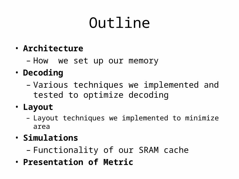
Outline
• Architecture– How we set up our memory
• Decoding– Various techniques we implemented and tested to
optimize decoding• Layout
– Layout techniques we implemented to minimize area
• Simulations– Functionality of our SRAM cache
• Presentation of Metric
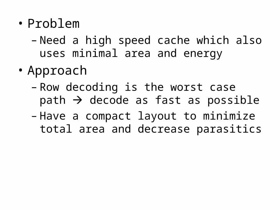
• Problem– Need a high speed cache which also uses minimal
area and energy
• Approach– Row decoding is the worst case path decode as
fast as possible– Have a compact layout to minimize total area and
decrease parasitics
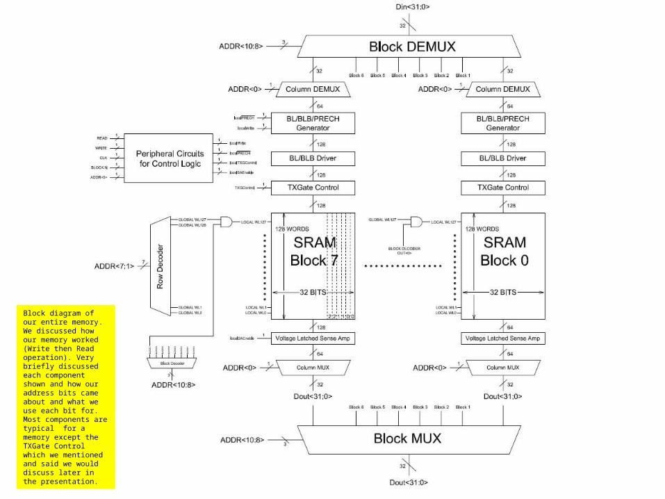
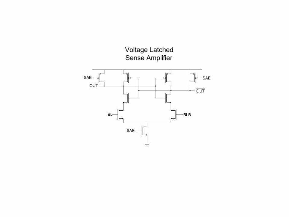
Block diagram of our entire memory. We discussed how our memory worked (Write then Read operation). Very briefly discussed each component shown and how our address bits came about and what we use each bit for. Most components are typical for a memory except the TXGate Control which we mentioned and said we would discuss later in the presentation.
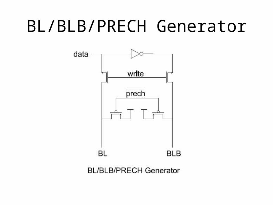
BL/BLB/PRECH Generator
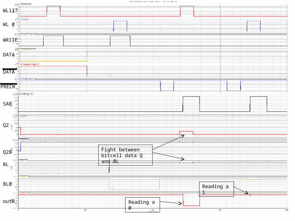
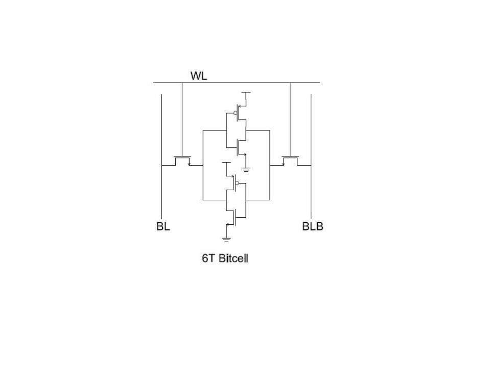
Fight between bitcell data Q and BL
WL127
WL 0
WRITE
DATA
DATA
PRECH
SAE
Q2
Q2B
BL
BLB
out0 Reading a 0
Reading a 1
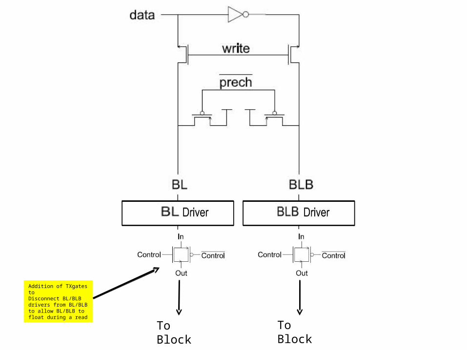
To Block To Block
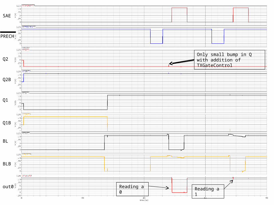
Addition of TXgates toDisconnect BL/BLB drivers from BL/BLB to allow BL/BLB to float during a read
SAE
PRECH
Q2
Q2B
Q1
Q1B
BL
BLB
out0
Only small bump in Q with addition of TXGateControl
Reading a 0 Reading a 1
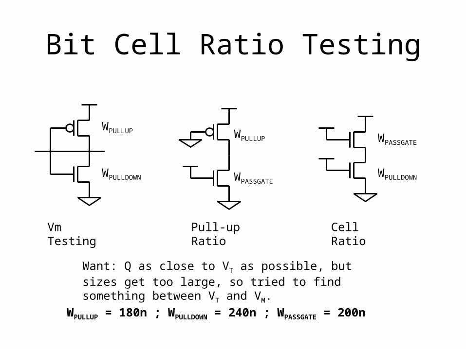
Bit Cell Ratio Testing
Vm Testing Pull-up Ratio Cell Ratio
WPULLUP WPULLUP
WPULLDOWN WPULLDOWN
WPASSGATE
WPASSGATE
Want: Q as close to VT as possible, but sizes get too large, so tried to find something between VT and VM.
WPULLUP = 180n ; WPULLDOWN = 240n ; WPASSGATE = 200n
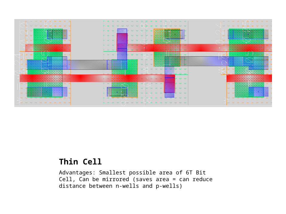
Thin CellAdvantages: Smallest possible area of 6T Bit Cell, Can be mirrored (saves area = can reduce distance between n-wells and p-wells)
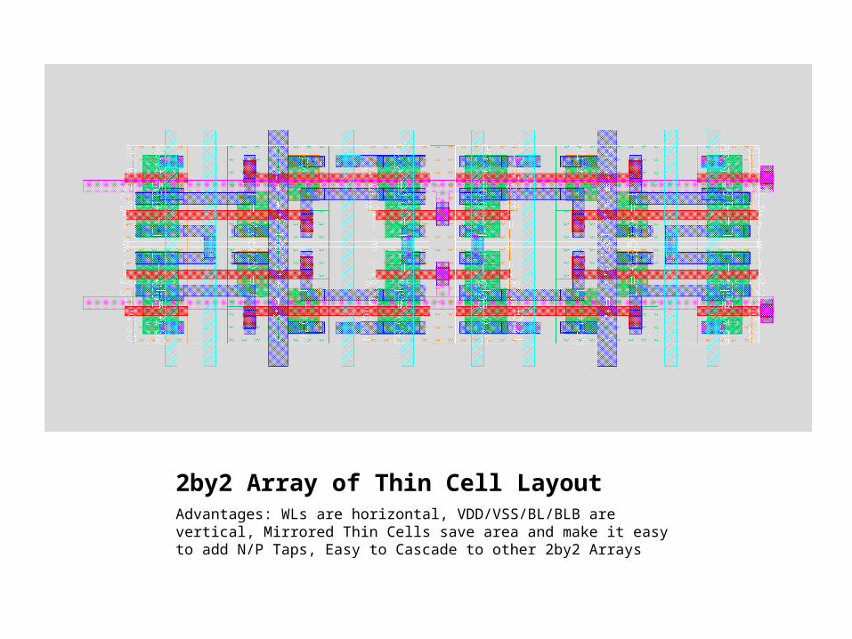
2by2 Array of Thin Cell LayoutAdvantages: WLs are horizontal, VDD/VSS/BL/BLB are vertical, Mirrored Thin Cells save area and make it easy to add N/P Taps, Easy to Cascade to other 2by2 Arrays
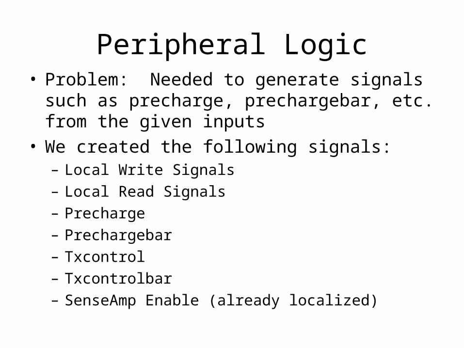
Peripheral Logic• Problem: Needed to generate signals such as
precharge, prechargebar, etc. from the given inputs• We created the following signals:
– Local Write Signals– Local Read Signals– Precharge– Prechargebar– Txcontrol– Txcontrolbar– SenseAmp Enable (already localized)
Decoding
• Need: High Speed• Decoding the proper row location is on critical
path• Considered numerous options
– Static– Dynamic
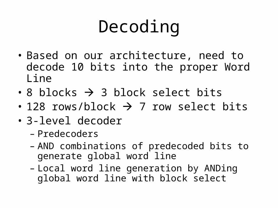
Decoding
• Based on our architecture, need to decode 10 bits into the proper Word Line
• 8 blocks 3 block select bits• 128 rows/block 7 row select bits• 3-level decoder
– Predecoders– AND combinations of predecoded bits to generate
global word line– Local word line generation by ANDing global word line
with block select
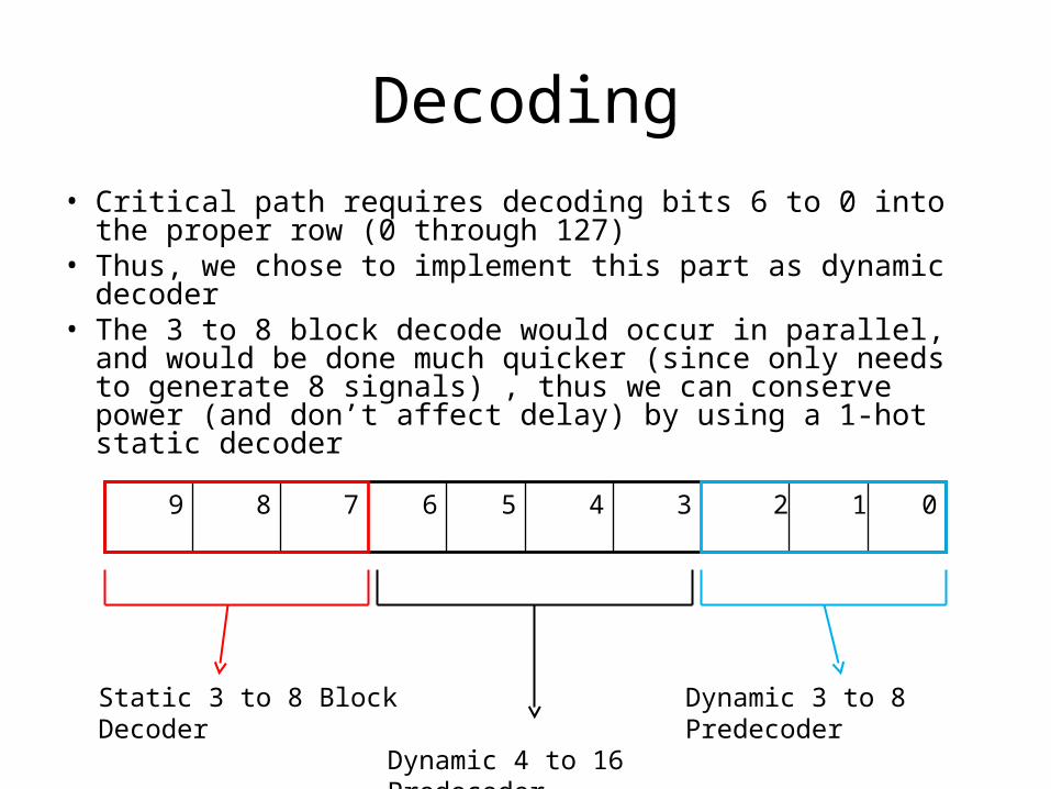
Decoding• Critical path requires decoding bits 6 to 0 into the proper
row (0 through 127)• Thus, we chose to implement this part as dynamic decoder• The 3 to 8 block decode would occur in parallel, and would
be done much quicker (since only needs to generate 8 signals) , thus we can conserve power (and don’t affect delay) by using a 1-hot static decoder
Static 3 to 8 Block Decoder
9 8 7 6 5 4 3 2 1 0
Dynamic 3 to 8 Predecoder
Dynamic 4 to 16 Predecoder
Decoding
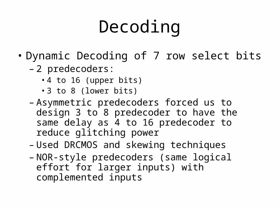
• Dynamic Decoding of 7 row select bits– 2 predecoders:
• 4 to 16 (upper bits)• 3 to 8 (lower bits)
– Asymmetric predecoders forced us to design 3 to 8 predecoder to have the same delay as 4 to 16 predecoder to reduce glitching power
– Used DRCMOS and skewing techniques– NOR-style predecoders (same logical effort for
larger inputs) with complemented inputs
Decoding
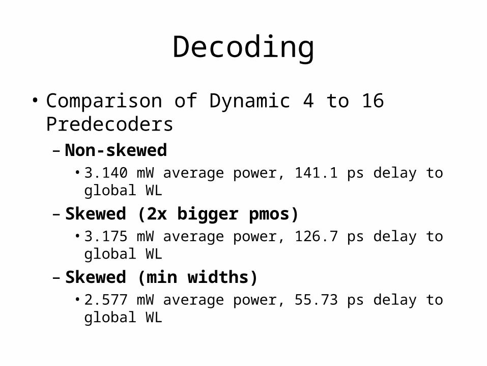
• Comparison of Dynamic 4 to 16 Predecoders– Non-skewed
• 3.140 mW average power, 141.1 ps delay to global WL
– Skewed (2x bigger pmos)• 3.175 mW average power, 126.7 ps delay to global WL
– Skewed (min widths)• 2.577 mW average power, 55.73 ps delay to global WL
Decoding
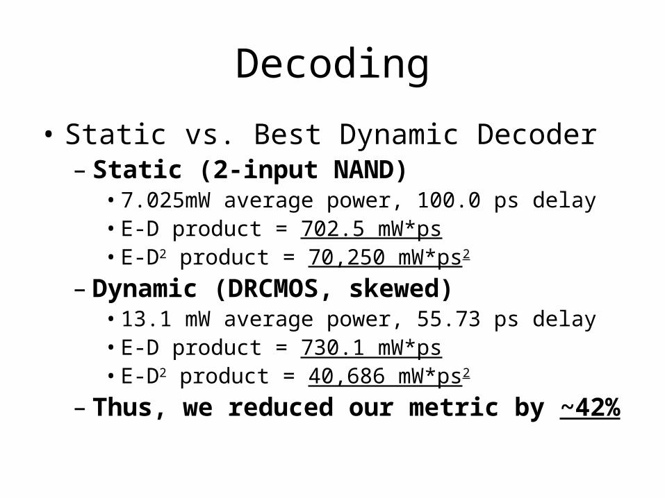
• Static vs. Best Dynamic Decoder– Static (2-input NAND)
• 7.025mW average power, 100.0 ps delay• E-D product = 702.5 mW*ps• E-D2 product = 70,250 mW*ps2
– Dynamic (DRCMOS, skewed)• 13.1 mW average power, 55.73 ps delay• E-D product = 730.1 mW*ps• E-D2 product = 40,686 mW*ps2
– Thus, we reduced our metric by ~42%
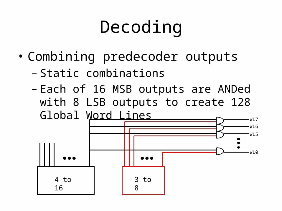
Decoding
• Combining predecoder outputs– Static combinations– Each of 16 MSB outputs are ANDed with 8 LSB
outputs to create 128 Global Word Lines
4 to 16 3 to 8
WL0
WL5
WL6WL7
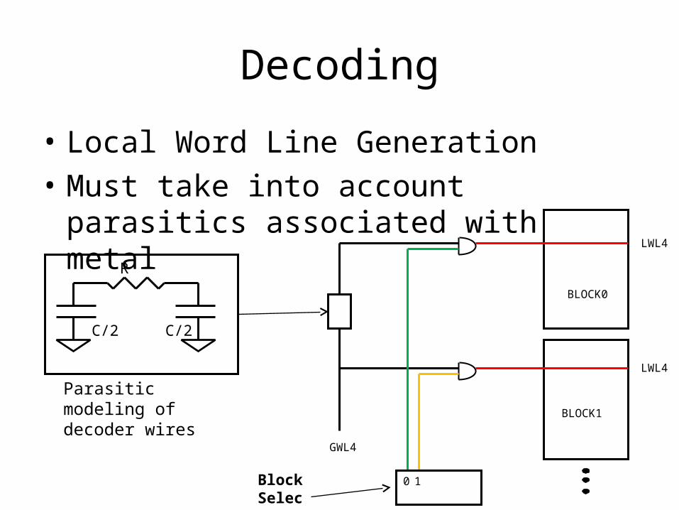
Decoding
• Local Word Line Generation• Must take into account parasitics associated
with long metal
GWL4
LWL4
LWL4
BLOCK1
BLOCK0
0 1Block Select
Parasitic modeling of decoder wires
C/2
R
C/2
Decoding
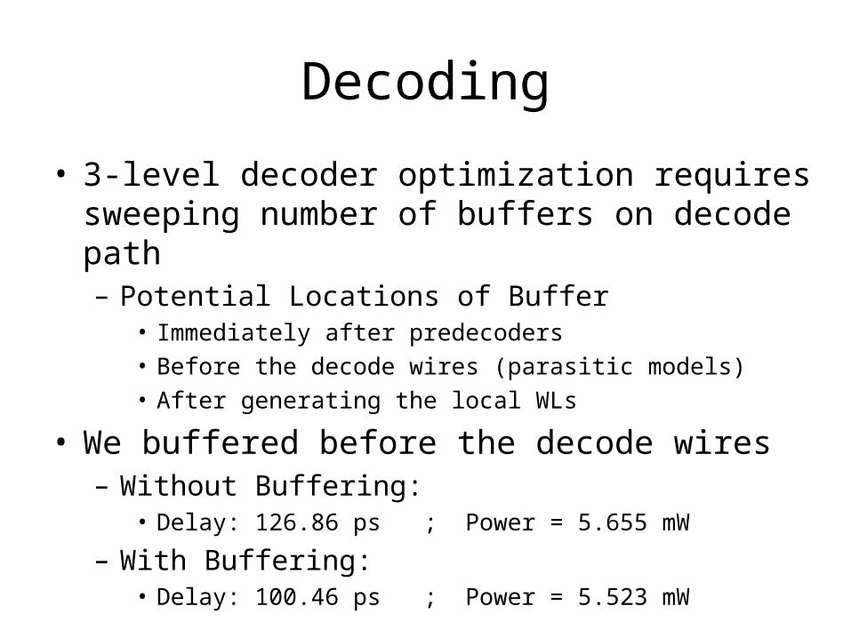
• 3-level decoder optimization requires sweeping number of buffers on decode path– Potential Locations of Buffer
• Immediately after predecoders• Before the decode wires (parasitic models)• After generating the local WLs
• We buffered before the decode wires– Without Buffering:
• Delay: 126.86 ps ; Power = 5.655 mW
– With Buffering:• Delay: 100.46 ps ; Power = 5.523 mW
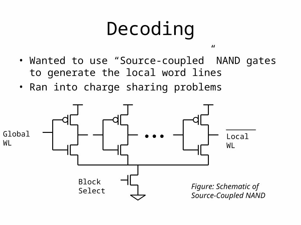
Decoding
• Wanted to use “Source-coupled” NAND gates to generate the local word lines
• Ran into charge sharing problems
Local WLGlobal WL
Block SelectFigure: Schematic of Source-Coupled NAND
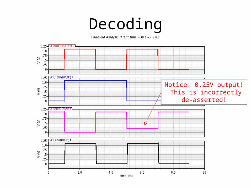
Decoding
Notice: 0.25V output! This is incorrectly de-asserted!
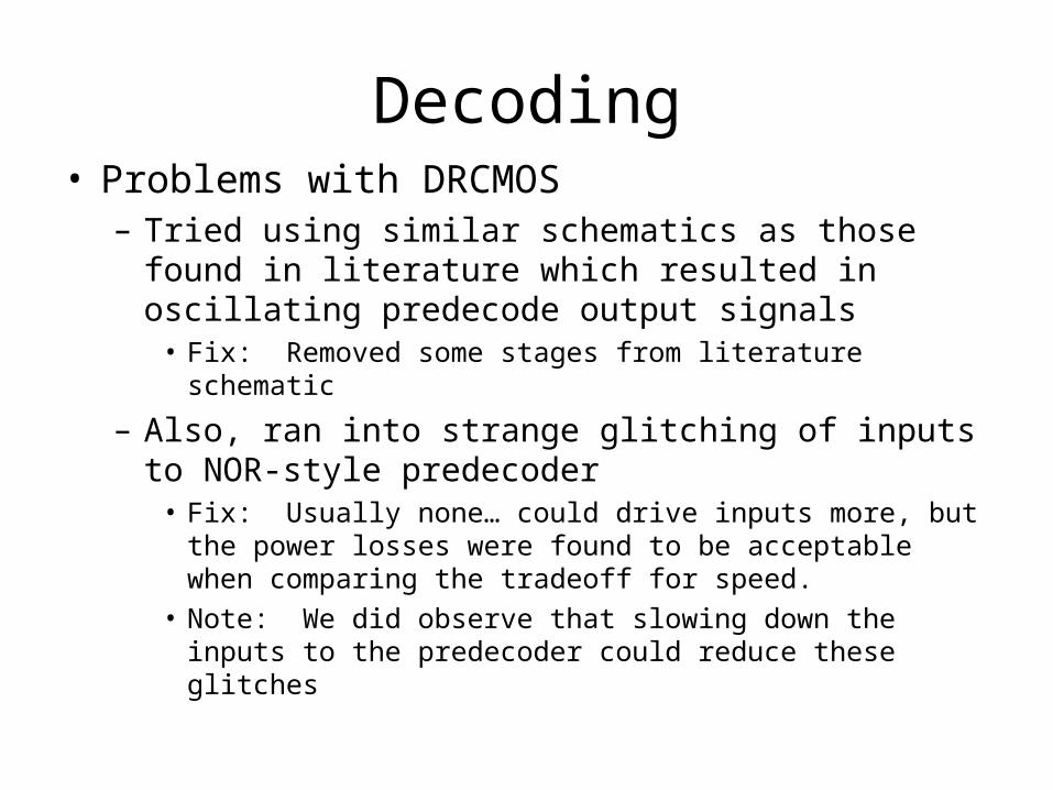
Decoding• Problems with DRCMOS
– Tried using similar schematics as those found in literature which resulted in oscillating predecode output signals
• Fix: Removed some stages from literature schematic
– Also, ran into strange glitching of inputs to NOR-style predecoder
• Fix: Usually none… could drive inputs more, but the power losses were found to be acceptable when comparing the tradeoff for speed.
• Note: We did observe that slowing down the inputs to the predecoder could reduce these glitches
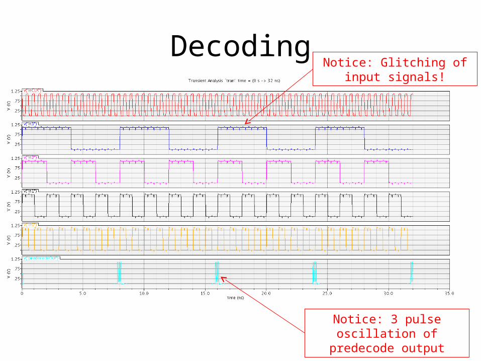
DecodingNotice: Glitching of input
signals!
Notice: 3 pulse oscillation of predecode output
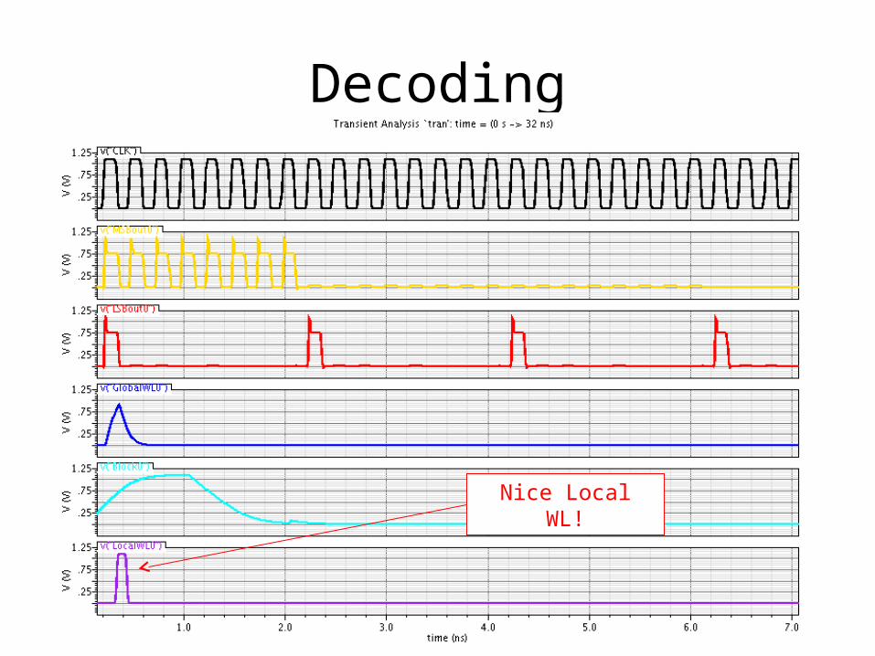
Decoding
Nice Local WL!
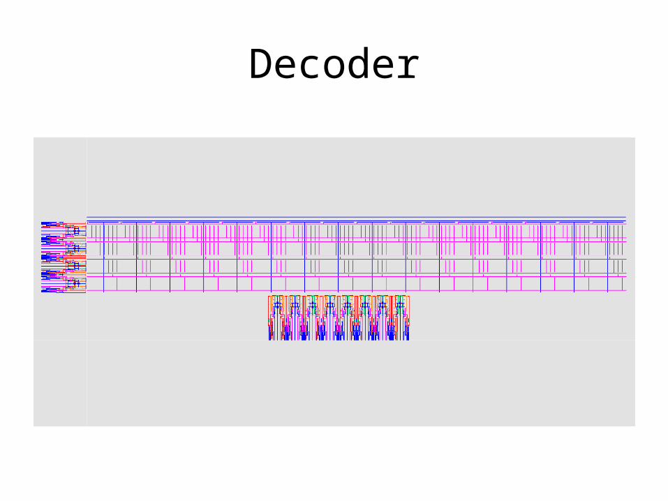
Decoder
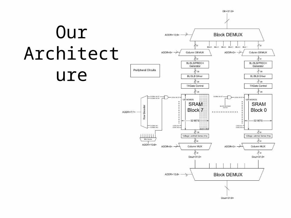
Our Architecture
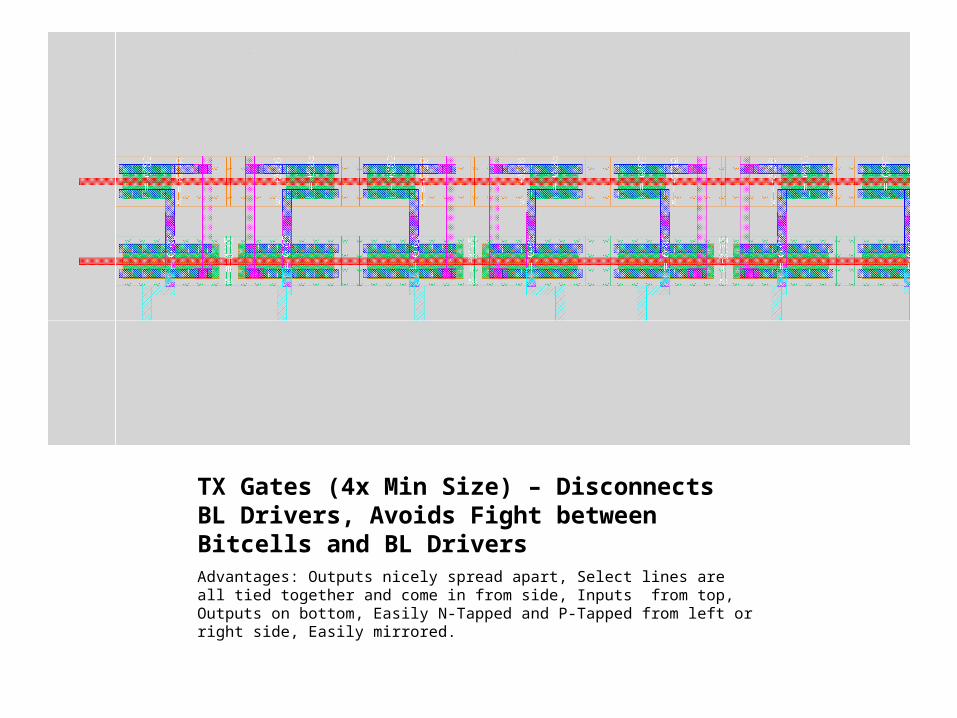
TX Gates (4x Min Size) – Disconnects BL Drivers, Avoids Fight between Bitcells and BL DriversAdvantages: Outputs nicely spread apart, Select lines are all tied together and come in from side, Inputs from top, Outputs on bottom, Easily N-Tapped and P-Tapped from left or right side, Easily mirrored.
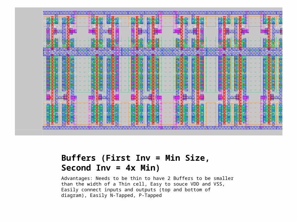
Buffers (First Inv = Min Size, Second Inv = 4x Min)Advantages: Needs to be thin to have 2 Buffers to be smaller than the width of a Thin cell, Easy to souce VDD and VSS, Easily connect inputs and outputs (top and bottom of diagram), Easily N-Tapped, P-Tapped
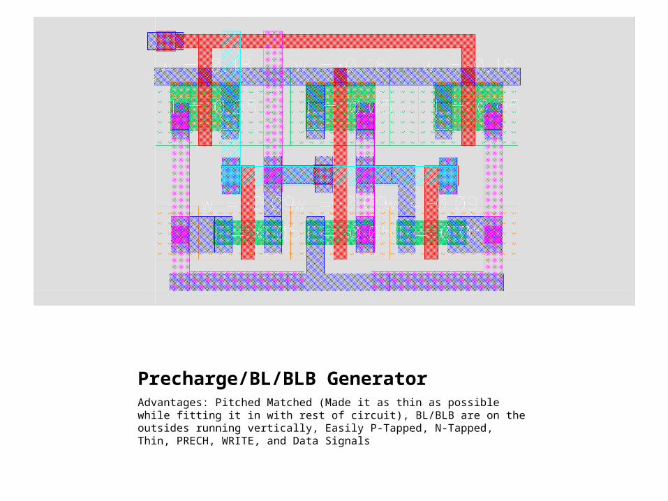
Precharge/BL/BLB GeneratorAdvantages: Pitched Matched (Made it as thin as possible while fitting it in with rest of circuit), BL/BLB are on the outsides running vertically, Easily P-Tapped, N-Tapped, Thin, PRECH, WRITE, and Data Signals
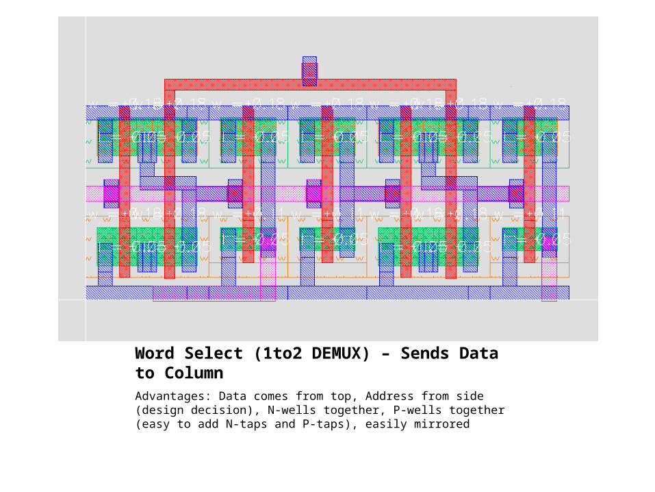
Word Select (1to2 DEMUX) – Sends Data to ColumnAdvantages: Data comes from top, Address from side (design decision), N-wells together, P-wells together (easy to add N-taps and P-taps), easily mirrored
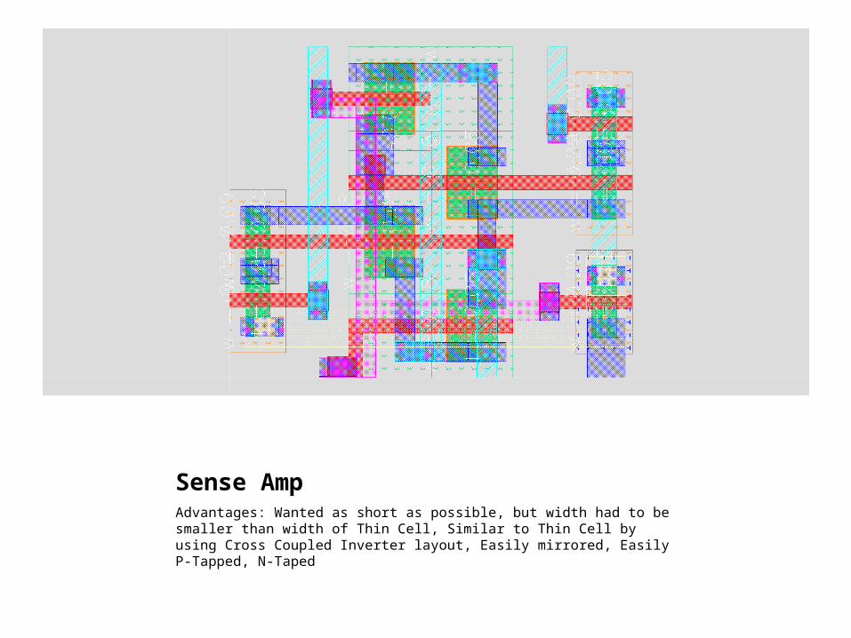
Sense AmpAdvantages: Wanted as short as possible, but width had to be smaller than width of Thin Cell, Similar to Thin Cell by using Cross Coupled Inverter layout, Easily mirrored, Easily P-Tapped, N-Taped
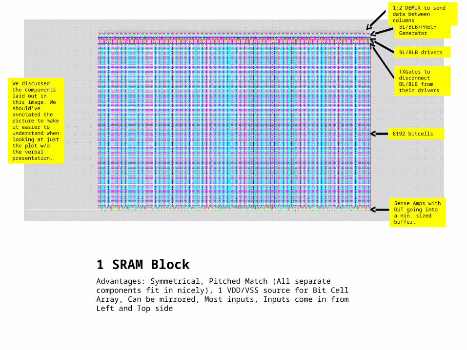
1 SRAM BlockAdvantages: Symmetrical, Pitched Match (All separate components fit in nicely), 1 VDD/VSS source for Bit Cell Array, Can be mirrored, Most inputs, Inputs come in from Left and Top side
We discussed the components laid out in this image. We should’ve annotated the picture to make it easier to understand when looking at just the plot w/o the verbal presentation.
Sense Amps with OUT going into a min. sized buffer.
BL/BLB/PRECH Generator
TXGates to disconnect BL/BLB from their drivers
BL/BLB drivers
1:2 DEMUX to send data between columns
8192 bitcells
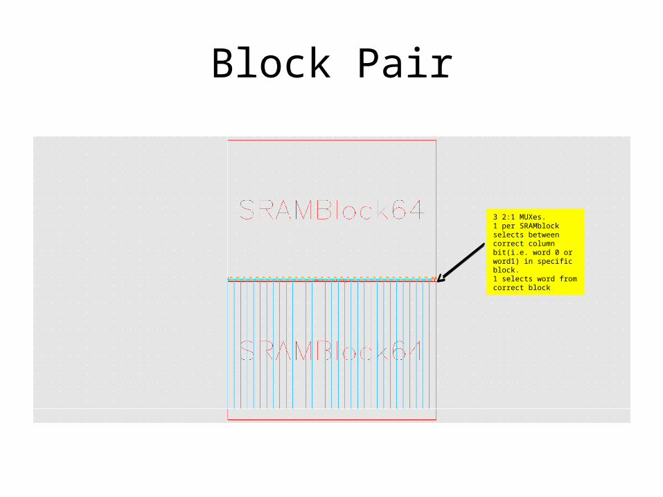
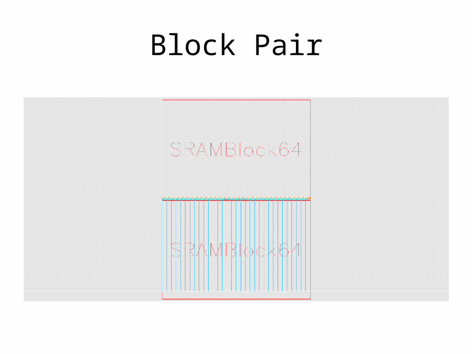
Block Pair
3 2:1 MUXes.1 per SRAMblock selects between correct column bit(i.e. word 0 or word1) in specific block.1 selects word from correct block
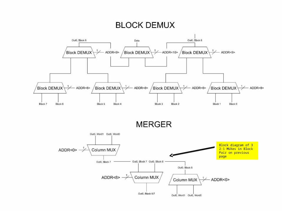
Block diagram of 3 2:1 MUXes in Block Pair on previous page
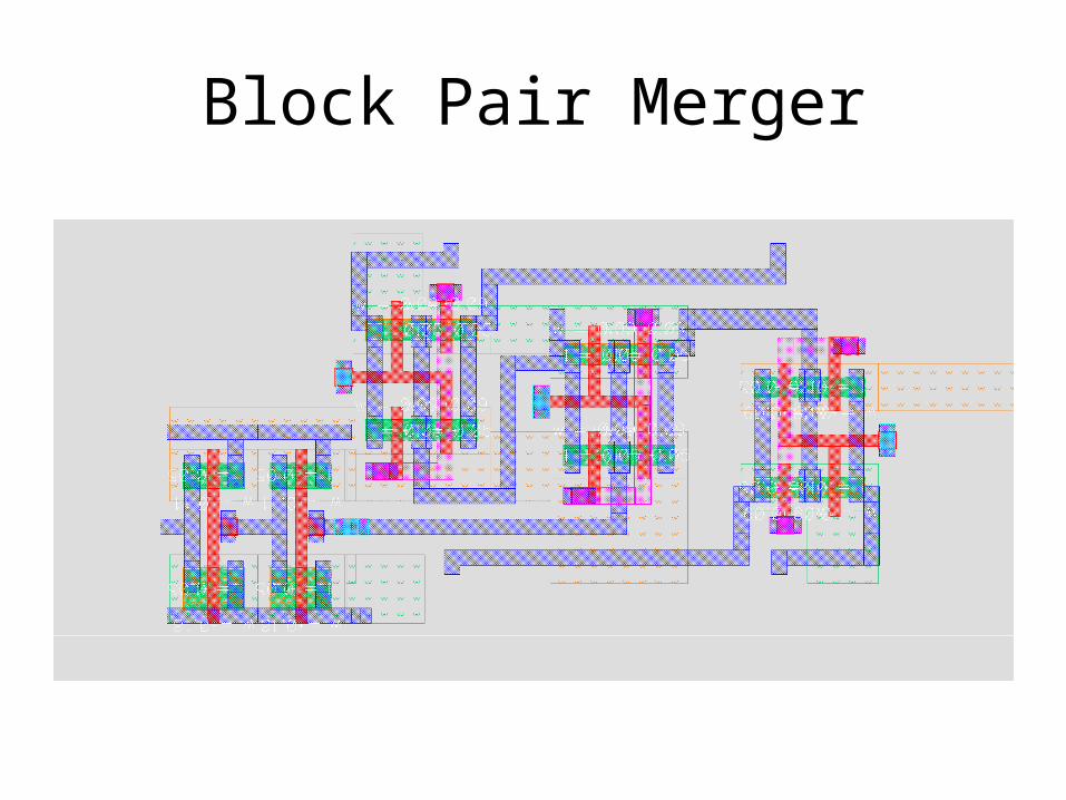
Block Pair Merger
Block Pair
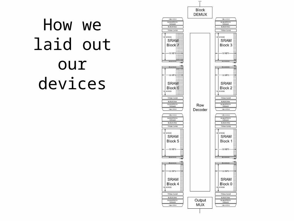
How we laid out our devices
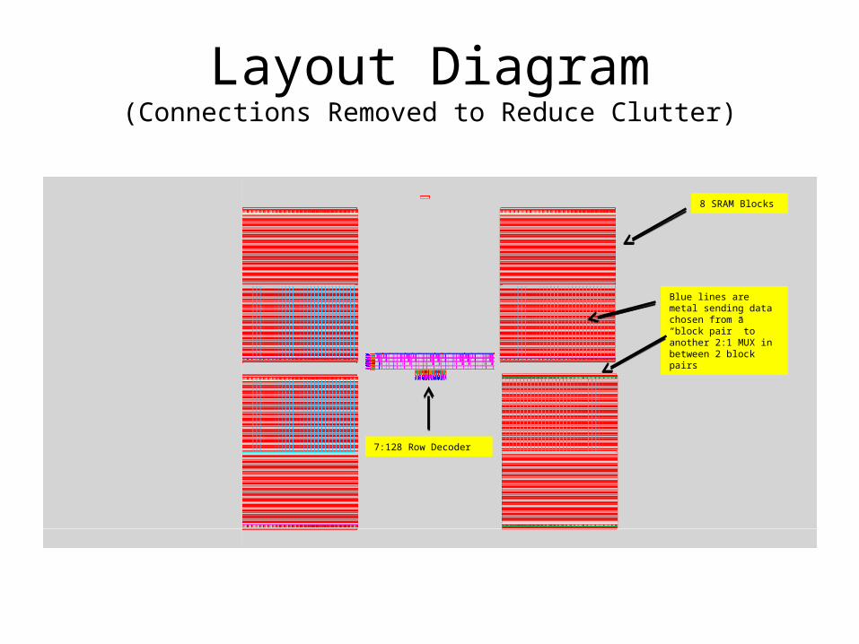
Layout Diagram(Connections Removed to Reduce Clutter)
8 SRAM Blocks
Blue lines are metal sending data chosen from a “block pair” to another 2:1 MUX in between 2 block pairs
7:128 Row Decoder
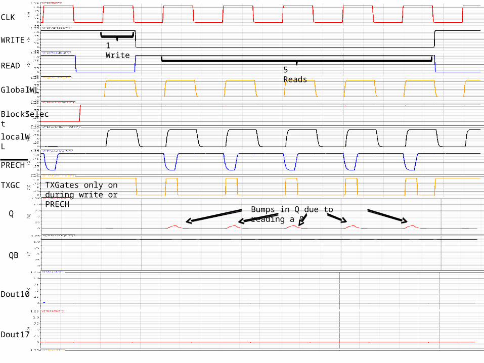
CLK
WRITE
READ
GlobalWL
BlockSelect
PRECH
localWL
TXGC
Q
QB
Dout10
Dout17
5 Reads
1 Write
Bumps in Q due to reading a 0
TXGates only on during write or PRECH
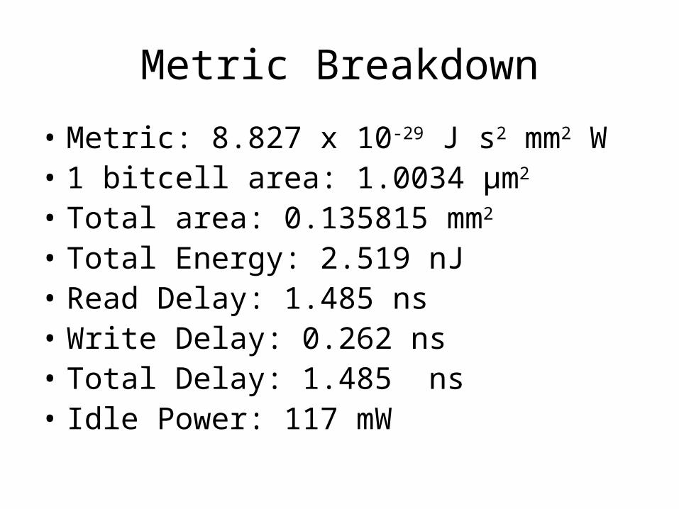
Metric Breakdown
• Metric: 8.827 x 10⁻²⁹ J s2 mm2 W• 1 bitcell area: 1.0034 µm2
• Total area: 0.135815 mm2
• Total Energy: 2.519 nJ• Read Delay: 1.485 ns• Write Delay: 0.262 ns• Total Delay: 1.485 ns• Idle Power: 117 mW

Questions?