high performance 32nm logic technology featuring … · iedm 2009 high performance 32nm logic...
TRANSCRIPT

IEDM 2009
High Performance 32nm Logic Technology Featuring 2nd Generation
High-k + Metal Gate Transistors
P. Packan, S. Akbar, M. Armstrong, D. Bergstrom, M. Brazier, H. Deshpande, K. Dev, G. Ding, T. Ghani, O. Golonzka, W. Han, J. He*, R. Heussner, R. James, J. Jopling, C. Kenyon, S-H. Lee, M. Liu, S. Lodha, B. Mattis, A. Murthy, L. Neiberg,
J. Neirynck, S. Pae*, C. Parker, L. Pipes, J. Sebastian, J. Seiple, B. Sell, A. Sharma, S. Sivakumar, B. Song, A. St. Amour, K. Tone, T. Troeger, C. Weber**,
K. Zhang, Y. Luo, S. Natarajan
Logic Technology Development, * Quality and Reliability Engineering, ** TCAD
Intel Corporation
IEDM 2009 2
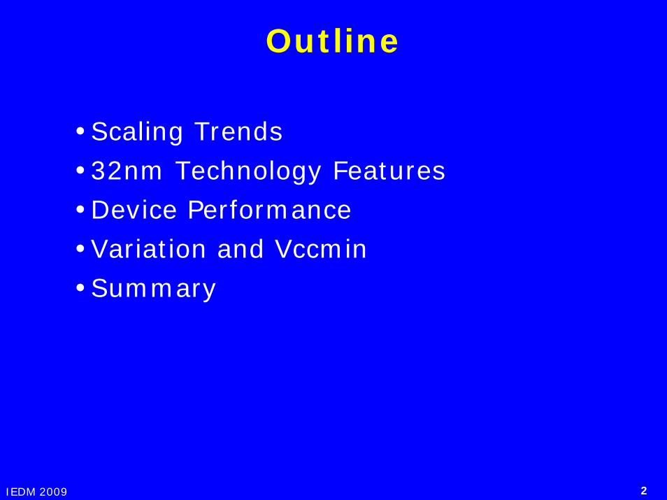
Outline
Scaling Trends32nm Technology FeaturesDevice PerformanceVariation and VccminSummary

IEDM 2009 3
Key Messages
32nm technology continues historic scaling trends–Reduced pitch and increased performance
Record NMOS and PMOS drive currents– NMOS Idsat of 1.62mA/um @100nA/um Ioff, 1.0V – PMOS Idsat of 1.37mA/um @100nA/um Ioff, 1.0V
Highest reported SRAM array density for any 32nm or 28nm technology

IEDM 2009 4
Outline
Scaling Trends32nm Technology FeaturesDevice PerformanceVariation and VccminSummary

IEDM 2009 5
Pitch Scaling Trend
Pitch scaling trend is continued to the 32nm technology node
PitchPitchPitch
100
1000
1995 2000 2005 2010
Gate Pitch (nm) 0.7x every
2 years
32nm
65nm
45nm
112.5 nm
Tightest reported gate pitch for Tightest reported gate pitch for any 32nm or 28nm nodeany 32nm or 28nm node

IEDM 2009 6
Pitch Scaling Issues
Reduced contact area increases resistanceReduced area for strain enhancementReduced gate length increases VtIncreased fringe capacitance
Novel techniques needed to scale pitch and Novel techniques needed to scale pitch and improve performanceimprove performance

IEDM 2009 7
Traditional Scaling
Junction scaling is slowing due to resistance increasesGate length scaling through increased Vt degrades performanceTraditional scaling is losing steam – new paradigm needed
Id=μCox/Le(Vg-Vt)α
0.20.30.40.50.60.70.80.9
11.1
0.015 0.025 0.035 0.045 0.055
IDLIN
IDSAT
VT0
0.2
0.4
0.6
0.8
1
1.2
0 0.02 0.04 0.06
IDLIN
REXT
VT
Junction ScalingJunction Scaling
Norm
aliz
ed V
alue
Tip Depth (um)
Vt ScalingVt ScalingN
orm
aliz
ed V
alue
Gate Length (um)

IEDM 2009 8
Gate Length and Drive Current
Longer gate lengths can improve drive current for the same Ioff due to the lower VtHowever, density and capacitance benefits at the shorter gate lengths are still preferred
0.E+00
2.E-08
4.E-08
6.E-08
8.E-08
1.E-07
1.E-07
0.7 0.8 0.9 1.0 1.1 1.2 1.3 1.4Normalized Idlin
Ioff
(A/u
m)
36nm Lg
32nm Lg
9%
Vds=0.05VVds=0.05V

IEDM 2009 9
Mobility Scaling
Increasing mobility increases device performance with minimal impact to leakage – effective scaling strategyReducing scattering mechanisms, applying stress and surface orientation all affect mobility
Id=μCox/Le(Vg-Vt)α
M.Giles, AVS 2006
(001) surface
1GPa uniaxial stress [110]
1 MV/cm vertical field
30meV energy contours
CB
D A
kx (2π/a)
k y(2π/
a)
0.2
0.1
0
-0.1
-0.20.20.10-0.1-0.2
C
D
B
kx (2π/a)
k y(2π/
a)A
0.2
0.1
0
-0.1
-0.20.20.10-0.1-0.2
Unstressed Stressed

IEDM 2009 10
Capping Layers Gate Induced
Contacts
Stress Methods
Epitaxial LayersC. Auth, VLSI 2008

IEDM 2009 11
NP Ratio Trend
PMOS drive strength has been increasing more rapidly than NMOS primarily due to mobility improvements from stressHole mobility shows a greater sensitivity to stress for (100)
– Valence band degeneracy– Band energy splitting– Band warping
Affects device sizing in circuits– Balances inverter circuits– Reduces PMOS area
Improves performance and power
hhhh
Electrons Holes
Technology Node
N/P
Idsa
t Rat
io
250 180 130 90 65 45
2.5
2.0
1.5
1.032
Introduction ofIntroduction ofStrained EpiStrained Epi

IEDM 2009 12
Idlin versus Idsat
• As an inverter switches, the transistor bias changes mapping out a current trajectory
• For typical capacitive loads, the majority of charging occurs at lower Vds values
• Based on these trajectories, Idsat may not be a good figure of merit for performance
• Idlin and Idsat are equally important for circuit performance
0.0E+00
2.0E-04
4.0E-04
6.0E-04
8.0E-04
1.0E-03
1.2E-03
1.4E-03
1.6E-03
1.8E-03
0 0.2 0.4 0.6 0.8 1Vds(V)
ID (A
)
ID(m)load = 2fFload = 4fFload = 10fF
Idsat
Idlin

IEDM 2009 13
Outline
Scaling Trends32nm Technology FeaturesDevice PerformanceVariation and VccminSummary

IEDM 2009 14
32nm Design Rules
Layer Pitch (nm) Thick (nm) Aspect Ratio
Isolation 140 200
35
95
95
95
151
204
303
Metal 7 450.1 388 1.7
Metal 8 566.5 504 1.8
8um
--
Contacted Gate 112.5 --
Metal 1 112.5 1.7
Metal 2 112.5 1.7
Metal 3 112.5 1.7
Metal 4 168.8 1.8
Metal 5 225.0 1.8
Metal 6 337.6 1.8
Metal 9 19.4um 1.5
~0.7x scaling from 45nm technology~0.7x scaling from 45nm technology

IEDM 2009 15
Interconnects
9 metal layers
Metal 1-3 pitches match transistor pitch
Graduated upper level pitches optimized for density and performance
Extensive use of low-k ILD and SiCN materials

IEDM 2009 16
Thick Top Metal Layer
Thick top metal for power delivery and I/O routing
IEDM 2009 17
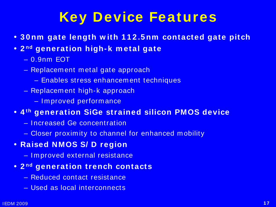
Key Device Features30nm gate length with 112.5nm contacted gate pitch2nd generation high-k metal gate– 0.9nm EOT– Replacement metal gate approach
– Enables stress enhancement techniques– Replacement high-k approach
– Improved performance
4th generation SiGe strained silicon PMOS device– Increased Ge concentration– Closer proximity to channel for enhanced mobility
Raised NMOS S/D region– Improved external resistance
2nd generation trench contacts– Reduced contact resistance– Used as local interconnects

IEDM 2009 18
Replacement Metal Gate Benefits
High Thermal budget available for Midsection– Better Activation of S/D Implants
Low thermal budget for Metal Gate– Large range of gate materials available
Significant enhancement of strain– Both NMOS and PMOS benefits

IEDM 2009 19
NMOSNMOS PMOSPMOS
Device Cross Sections

IEDM 2009 20
NMOSNMOS PMOSPMOS
Device Cross Sections
30nm gate length devices112.5nm contacted gate pitch
112.5nm
30nm
112.5nm
30nm

IEDM 2009 21
NMOSNMOS PMOSPMOS
Device Cross Sections
2nd generation high-k dual work function metal gateReplacement metal gate and high-k flow for improved performance

IEDM 2009 22
NMOSNMOS PMOSPMOS
Device Cross Sections
4th generation strained SiGe PMOS epi layer Increased Ge content and closer proximity to channel for higher strain
IEDM 2009 23
NMOSNMOS PMOSPMOS
Device Cross Sections
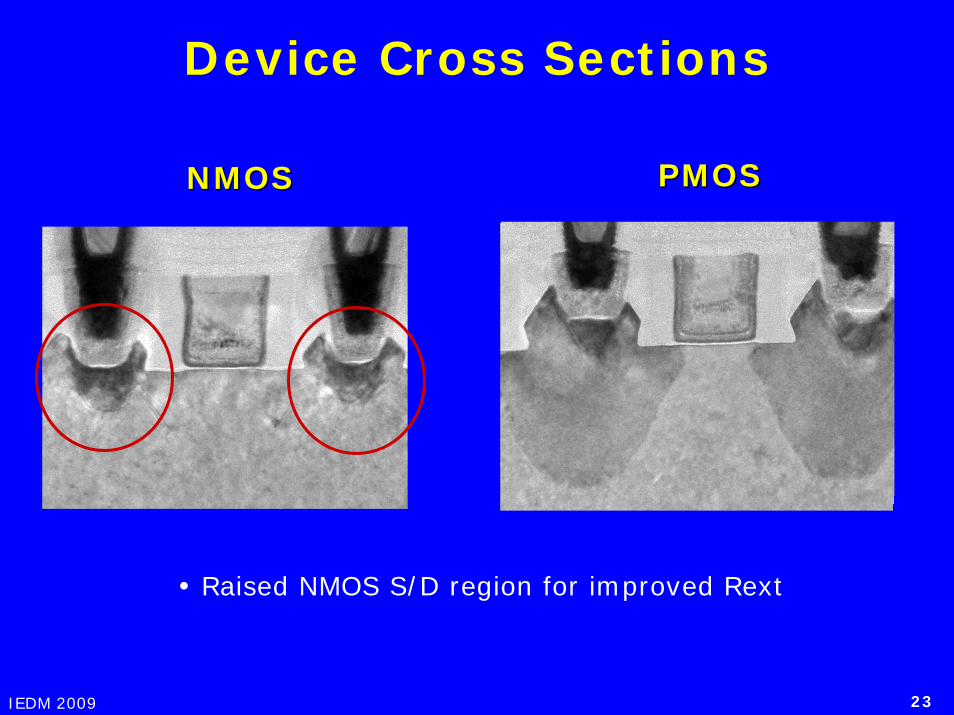
Raised NMOS S/D region for improved Rext

IEDM 2009 24
NMOSNMOS PMOSPMOS
Device Cross Sections
Dual trench contacts with tungsten lower layer and copper upper layerTrench contacts for improved resistance and local interconnects

IEDM 2009 25
PMOS Mobility Scaling
65 nm
23%31nm
45 nm
30%21nm
32 nm
40%12nm
90 nm
17%50nm
Increasing Ge ConcentrationIncreasing Ge Concentration
Closer ProximityCloser Proximity
RMG Strain Enhancement RMG Strain Enhancement
Increasing Ge concentration and closer SiGe proximity improves drive Strain enhancement possible only in the RMG flow also improves drive

IEDM 2009 26
1
2
3
4
90nm 65nm 45nm 32nm
Stress and Mobility Enhancement
0
500
1000
1500
2000
2500
90nm 65nm 45nm 32nm
TechnologyTechnology
Str
ess
(MPa
)Str
ess
(MPa
)
Stress ScalingStress Scaling
TechnologyTechnology
Mobili
ty E
nhan
cem
ent
Mobili
ty E
nhan
cem
ent Mobility ScalingMobility Scaling
Innovations enable performance and pitch scaling

IEDM 2009 27
Outline
Scaling Trends32nm Technology FeaturesDevice PerformanceVariation and VccminSummary

IEDM 2009 28
NMOS Performance
1.62mA/um Idsat and 0.231mA/um Idlin @ 100nA Ioff 19% and 20% gain over 45nm
1
10
100
1000
Ioff
(nA
/um
)0.18 0.2 0.22 0.24 0.26
Idlin (mA/um)
45nm0.192mA/um
This work0.231mA/um@100nA/um Ioff112.5nm pitch
20%20%
Vgs=1.0V Vgs=1.0V Vds=0.05Vds=0.05
45nm: Mistry 2007 IEDM
1
10
100
1000
Ioff
(nA
/um
)
1 1.2 1.4 1.6 1.8 2Idsat (mA/um)
This work1.62mA/um@100nA/um Ioff112.5nm pitch
45nm1.36mA/um 19%19%
Vgs=1.0VVgs=1.0VVds=1.0VVds=1.0V
45nm: Mistry 2007 IEDM

IEDM 2009 29
PMOS Performance
1.37mA/um Idsat and 0.240mA/um Idlin @ 100nA Ioff28% and 35% gain over 45nm
1
10
100
1000
Ioff
(nA
/um
)
0.8 1 1.2 1.4 1.6|Idsat| (mA/um)
This work1.37mA/um@100nA/um Ioff112.5nm pitch
45nm1.07mA/um 28%28%
45nm: Mistry 2007 IEDM
Vgs=1.0VVgs=1.0VVds=1.0VVds=1.0V
1
10
100
1000
Ioff
(nA
/um
)0.16 0.18 0.2 0.22 0.24 0.26 0.28
|Idlin| (mA/um)
45nm0.178mA/um
This work0.240mA/um@100nA/um Ioff112.5nm pitch
35%35%
45nm: Mistry 2007 IEDM
Vgs=1.0V Vgs=1.0V Vds=0.05Vds=0.05

IEDM 2009 30
IV Characteristics
PMOS drive currents are approaching NMOS valuesSubthreshold slopes are well maintained at ~100mV/decade
0
0.2
0.4
0.6
0.8
1
1.2
1.4
1.6
1.8
Id (m
A/u
m)
-1 -0.75 -0.5 -0.25 0 0.25 0.5 0.75 1Vds (V)
PMOSNMOS
1.0V
0.8V
0.6V
1e-9
1e-8
1e-7
1e-6
1e-5
1e-4
1e-3
1e-2
Id (A
/um
)-1 -0.75 -0.5 -0.25 0 0.25 0.5 0.75 1
Vgs (V)
PMOS NMOS
Vds=50mV
Vds=1.0V

IEDM 2009 31
Pitch and Performance Scaling
Simultaneous performance and density improvement
1001000 Gate Pitch (nm)
Drive Current (mA/um)
0.0
0.5
1.0
1.5
2.01.0 V, 100 nA IOFF
45nm
32nm
65nm90nm
NMOS
PMOS
130nm
Highest reported drive currents at tightest reported gate pitch of any 32nm or 28nm technology

IEDM 2009 32
Outline
Scaling Trends32nm Technology FeaturesDevice PerformanceVariation and VccminSummary

IEDM 2009 33
Device Variation
32nm technology continues the 0.7x reduction in CD variationNo increase in systematic and random variation is seen
Gate CD variation improvements with technology scaling
0.1
1
10
130nm 90nm 65nm 45nm 32nm
WIW-total TOTAL
WID-total 0.7X
LOG
(Nor
mal
ized
Var
iatio
n)
Generation
( )
0
1
2
3
4
5
130nm 90nm 65nm 45nm 32nm
PE
RC
EN
T (%
)
Systematic Variation
012
345
130nm 90nm 65nm 45nm 32nmP
ER
CE
NT
(%)
Random VariationK.KuhnK.Kuhn

IEDM 2009 34
SRAM Scaling Trend
Transistor density doubles every two years
32 nm, 0.171 um2
45 nm, 0.346 um2
65 nm, 0.570 um2
0.1
1
10
100
250nm180nm130nm 90nm 65nm 45nm
Source: Intel
Technology
0.5x everytwo years
32nm
SRAM
Cel
l Are
a (u
mSRAM
Cel
l Are
a (u
m22))

IEDM 2009 35
Array Density Scaling
Array density includes cells, sense amps and control circuitry
0.1
1
10
90nm 65nm 45nm 32nm
Technology Node
Arr
ay D
ensi
ty (M
b/m
m2 )
2x increase 2x increase per generationper generation
4.2Mb/mm4.2Mb/mm22
4.2Mbit/mm2 array density is the highest reported for any 32nm or 28nm technology

IEDM 2009 36
Cell Area and Vccmin
As expected, larger SRAM cell sizes support lower VccminVccmin depends on the distribution percentage reported
0.50 0.60 0.70 0.80
10
50
90
VccminP
erce
nt
1
99
0.90 1.0
0.171um2
0.199um2
0.256um2
3.25Mb array
Cell Area (/umCell Area (/um22))
Vcc
min
(V)
Vcc
min
(V)
0.5
0.55
0.6
0.65
0.7
0.75
0.8
0.15 0.2 0.25 0.3
3.25 Mb array

IEDM 2009 37
Cell Area and Vccmin
As expected, larger SRAM cell sizes support lower VccminVccmin depends on the distribution percentage reported
0.50 0.60 0.70 0.80
10
50
90
VccminP
erce
nt
1
99
0.90 1.0
0.171um2
0.199um2
0.256um2
150mV
3.25Mb array
Cell Area (/umCell Area (/um22))
Vcc
min
(V)
Vcc
min
(V)
0.5
0.55
0.6
0.65
0.7
0.75
0.8
0.15 0.2 0.25 0.3
3.25 Mb array

IEDM 2009 38
Cell Array Size and Vccmin
Vccmin increases for larger array sizes due to the statistics from the larger number of cells
0.6
0.65
0.7
0.75
0.8
0.85
0.1 1 10 100 1000Array Size (Mb)Array Size (Mb)
Vcc
min
@ 9
0%
(V)
Vcc
min
@ 9
0%
(V)
0.199um0.199um22
cell sizecell size

IEDM 2009 39
Cell Array Size and Vccmin
Vccmin increases for larger array sizes due to the statistics from the larger number of cells
0.6
0.65
0.7
0.75
0.8
0.85
0.1 1 10 100 1000Array Size (Mb)Array Size (Mb)
Vcc
min
@ 9
0%
(V)
Vcc
min
@ 9
0%
(V)
150mV150mV
0.199um0.199um22
cell sizecell size
IEDM 2009 40
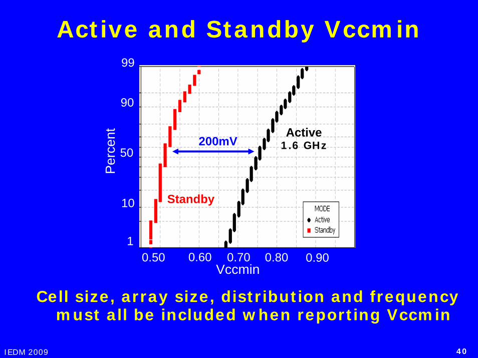
Active and Standby Vccmin
Cell size, array size, distribution and frequency must all be included when reporting Vccmin
99
0.50 0.60 0.70 0.80
10
50
90
Vccmin
Per
cent
10.90
200mVActive
Standby
1.6 GHz

IEDM 2009 41
Outline
Scaling Trends32nm Technology FeaturesDevice PerformanceVariation and VccminSummary

IEDM 2009 42
32 nm Defect Density Trend90 nm 65 nm 45 nm 32 nm
2002 2003 2004 2005 2006 2007 2008 2009 2010
Defect Density(log scale) <2 year
HigherYield
• Intel’s 32 nm process has achieved the high yields needed for volume production
• 32 nm CPU products are presently being produced and shipped from two factories

IEDM 2009 43
32 nm Westmere Microprocessor
Dual core WestmereIndustry’s first 32 nm processor
First in a family of 32 nm microprocessors based upon the Intel® microarchitecture codenamed Nehalem

IEDM 2009 44
Summary32nm technology continues historic scaling trends–Reduced pitch and increased performance
Record NMOS and PMOS drive currents– NMOS Idsat of 1.62mA/um @100nA/um Ioff, 1.0V – PMOS Idsat of 1.37mA/um @100nA/um Ioff, 1.0V
Highest reported SRAM array density and tightest reported gate pitch for any 32nm or 28nm technology
This 32nm technology is in high volume manufacturing of multi-core CPU products in multiple fabs
IEDM 2009 45
Acknowledgements
The authors gratefully acknowledge the many people in the following organizations at Intel who contributed to this work:–Logic Technology Development –Quality and Reliability Engineering–Technology CAD–Components Research–Assembly & Test Technology Development

IEDM 2009 46
For further information on Intel's silicon technology, please visit our Technology & Research page at
www.intel.com/technology