high-efficiency, multijunction solar cells for large-scale solar
TRANSCRIPT
High-efficiency, multijunction solar cells for large-scale solar
electricity generationSarah Kurtz
APS March Meeting, 2006
Acknowledge: Jerry Olson, John Geisz, Mark Wanlass, Bill McMahon, Dan Friedman, Scott Ward, Anna Duda, Charlene Kramer, Michelle Young, Alan Kibbler, Aaron Ptak, Jeff Carapella, Scott Feldman, Chris Honsberg (Univ. of Delaware), Allen Barnett (Univ. of Delaware), Richard King (Spectrolab), Paul Sharps (EMCORE)
Outline• Motivation - High efficiency adds value• The essence of high efficiency
– Choice of materials & quality of materials– Success so far - 39%
• Material quality– Avoid defects causing non-radiative recombination
• High-efficiency cells for the future– Limited only by our creativity to combine high-quality
materials• The promise of concentrator systems
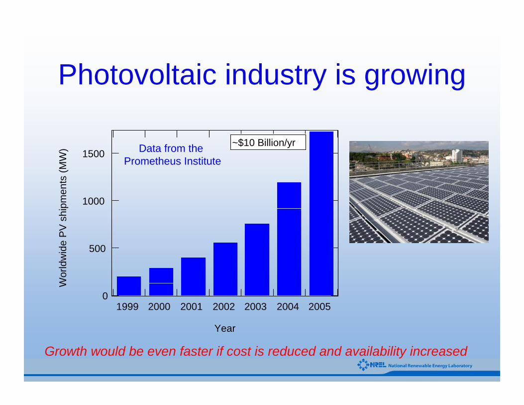
Photovoltaic industry is growing
Growth would be even faster if cost is reduced and availability increased
1500
1000
500
0
Wor
ldw
ide
PV
shi
pmen
ts (M
W)
1999 2000 2001 2002 2003 2004 2005
Year
~$10 Billion/yrData from thePrometheus Institute
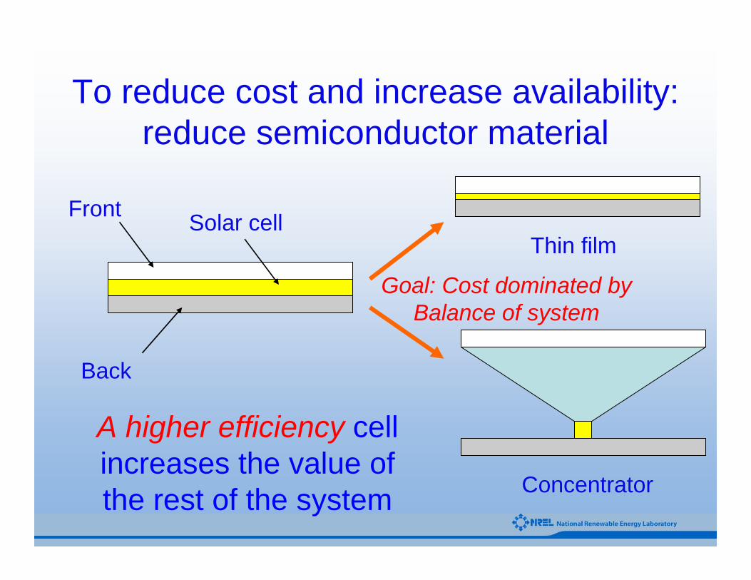
To reduce cost and increase availability: reduce semiconductor material
Front Solar cell
Back
Thin film
Concentrator
A higher efficiency cell increases the value of the rest of the system
Goal: Cost dominated by Balance of system
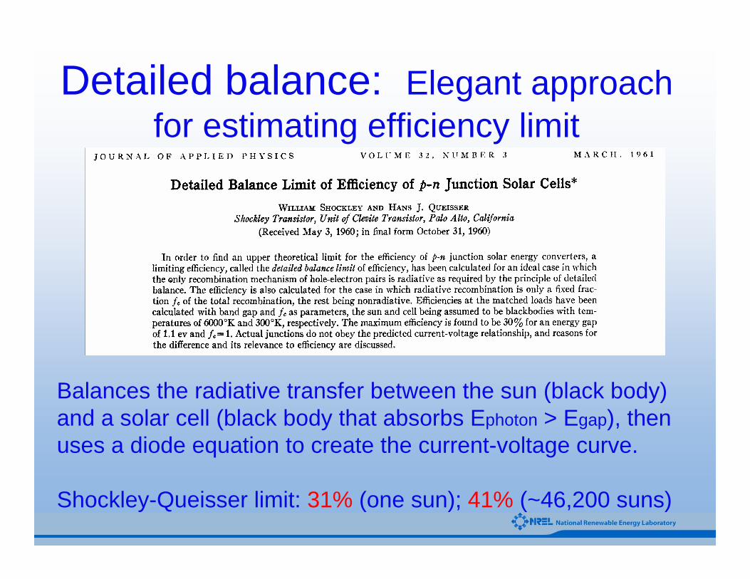
Detailed balance: Elegant approach for estimating efficiency limit
Balances the radiative transfer between the sun (black body) and a solar cell (black body that absorbs Ephoton > Egap), then uses a diode equation to create the current-voltage curve.
Shockley-Queisser limit: 31% (one sun); 41% (~46,200 suns)
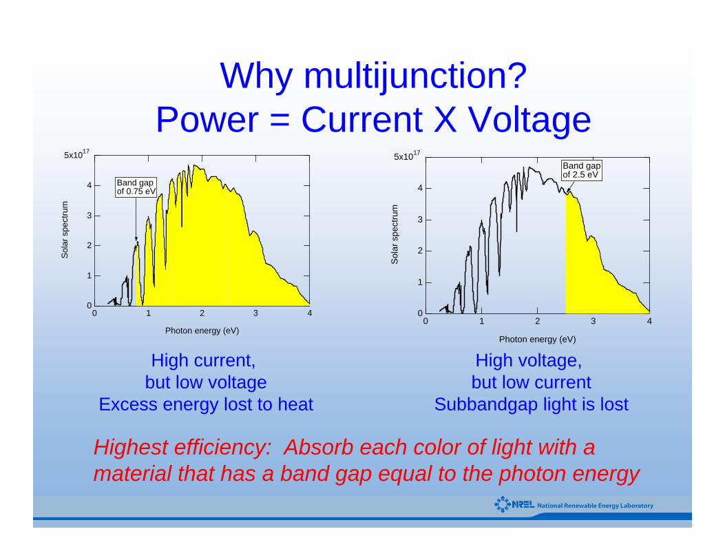
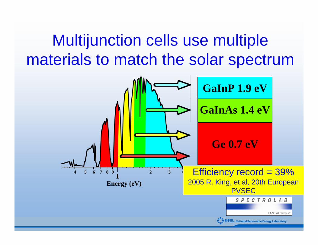
Why multijunction?Power = Current X Voltage
5x10¹⁷
4
3
2
1
0
Sol
ar s
pect
rum
43210
Photon energy (eV)
Band gapof 0.75 eV
5x10¹⁷
4
3
2
1
0
Sol
ar s
pect
rum
43210
Photon energy (eV)
Band gapof 2.5 eV
High current,but low voltage
Excess energy lost to heat
High voltage,but low current
Subbandgap light is lost
Highest efficiency: Absorb each color of light with a material that has a band gap equal to the photon energy
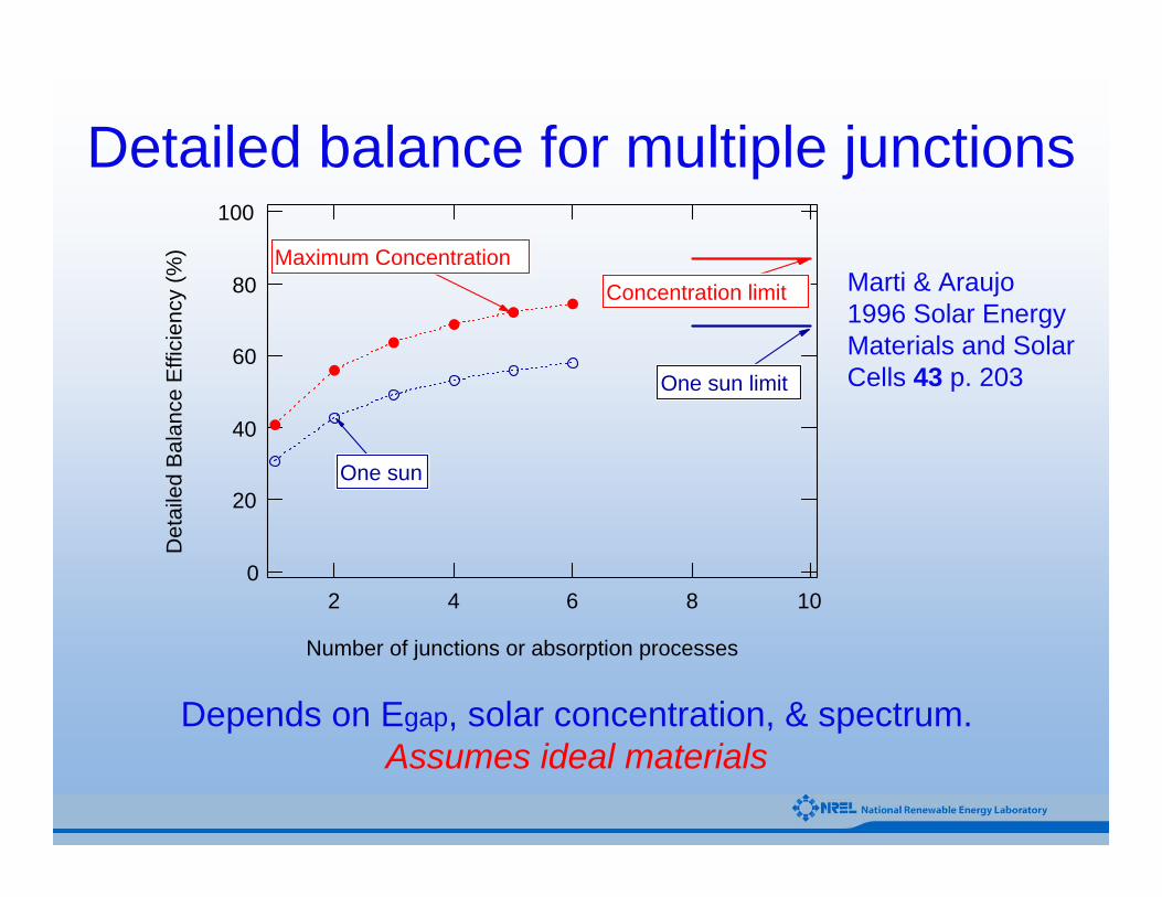
Detailed balance for multiple junctions
Depends on Egap, solar concentration, & spectrum. Assumes ideal materials
100
80
60
40
20
0
Det
aile
d B
alan
ce E
ffici
ency
(%)
108642
Number of junctions or absorption processes
One sun limit
One sun
Concentration limitMaximum Concentration
Marti & Araujo1996 Solar Energy Materials and Solar Cells 43 p. 203
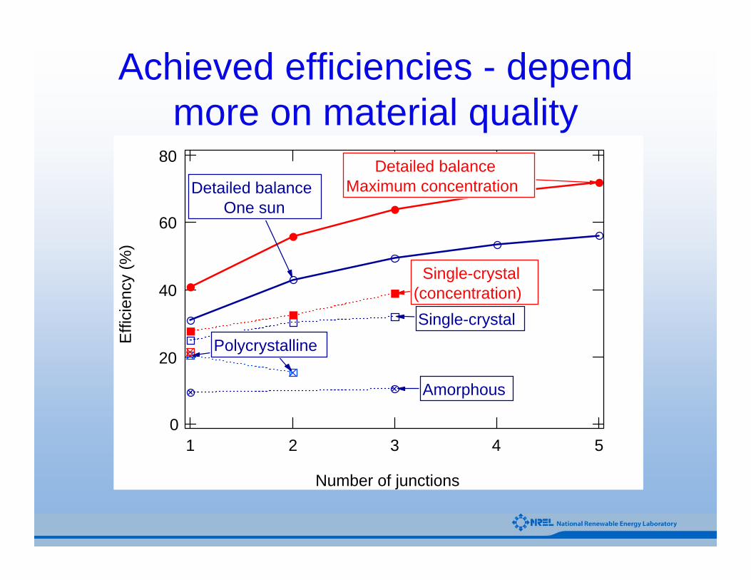
Achieved efficiencies - depend more on material quality
80
60
40
20
0
Effi
cien
cy (%
)
54321
Number of junctions
Detailed balanceOne sun
Detailed balanceMaximum concentration
Amorphous
PolycrystallineSingle-crystal
Single-crystal(concentration)
Polycrystalline
Effic
iency
(%)
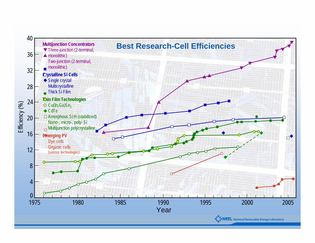
200019951990198519801975
Multijunction ConcentratorsThree-junction (2-terminal, monolithic)Two-junction (2-terminal, monolithic)
Crystalline Si CellsSingle crystalMulticrystallineThick Si Film
Thin Film TechnologiesCu(In,Ga)Se2CdTeAmorphous Si:H (stabilized)Nano-, micro-, poly- SiMultijunction polycrystalline
Emerging PVDye cells Organic cells(various technologies)12
8
4
0
16
20
24
28
32
36
2005
40Best Research-Cell Efficiencies
Year
p4 5 6 7 8 9
12 3 4
Energy (eV)
Ge 0.7 eV
GaInAs 1.4 eV
GaInP 1.9 eV
Efficiency record = 39%2005 R. King, et al, 20th European
PVSEC
Multijunction cells use multiplematerials to match the solar spectrum
40
30
20
10
0
Effi
cien
cy (%
)
20052000199519901985Year
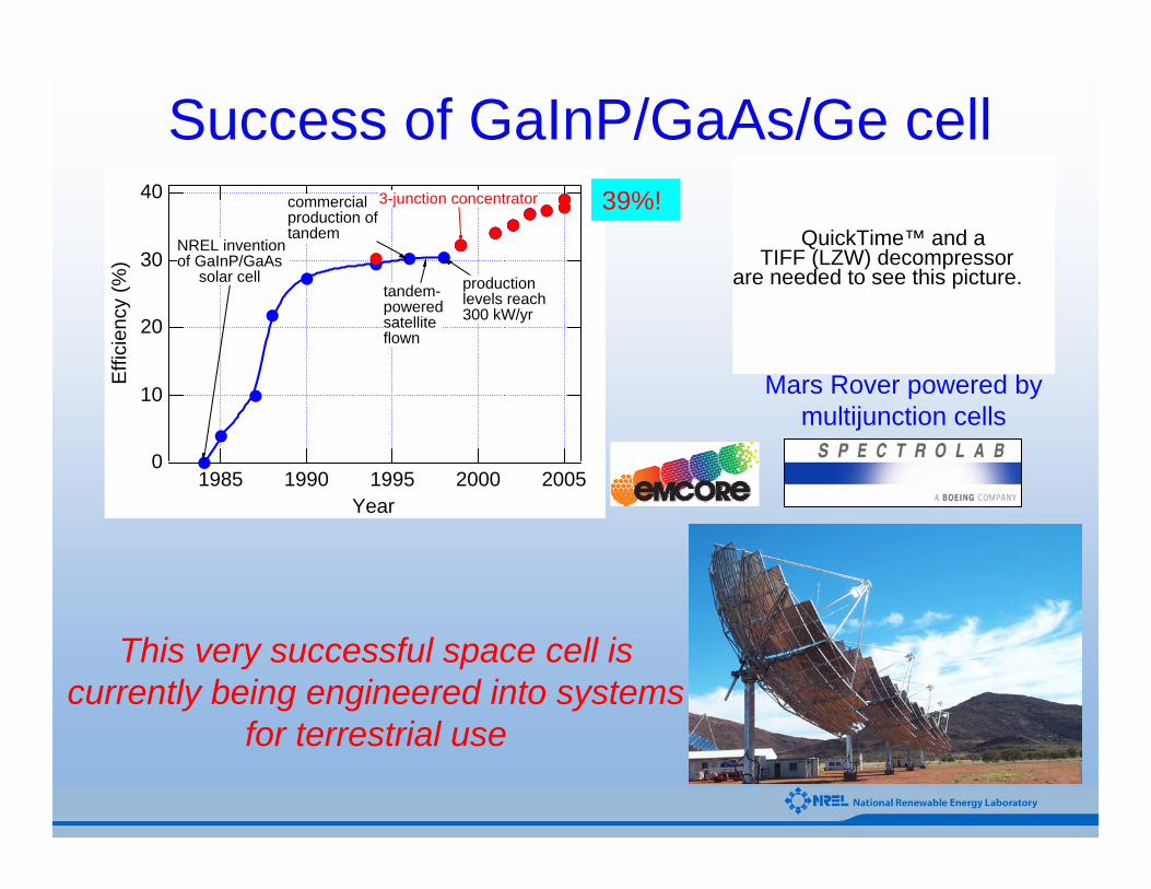
NREL invention of GaInP/GaAs solar cell
tandem-poweredsatelliteflown
commercialproduction oftandem
productionlevels reach300 kW/yr
3-junction concentrator
Success of GaInP/GaAs/Ge cell
QuickTime™ and aTIFF (LZW) decompressor
are needed to see this picture.
Mars Rover powered by multijunction cells
This very successful space cell is currently being engineered into systems
for terrestrial use
39%!
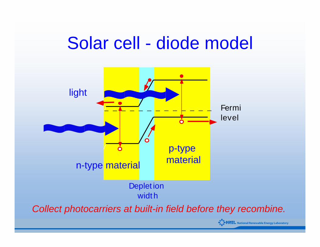
Solar cell - diode model
Collect photocarriers at built-in field before they recombine.
Fermilevel
Deplet ionwidt h
p-type materialn-type material
light
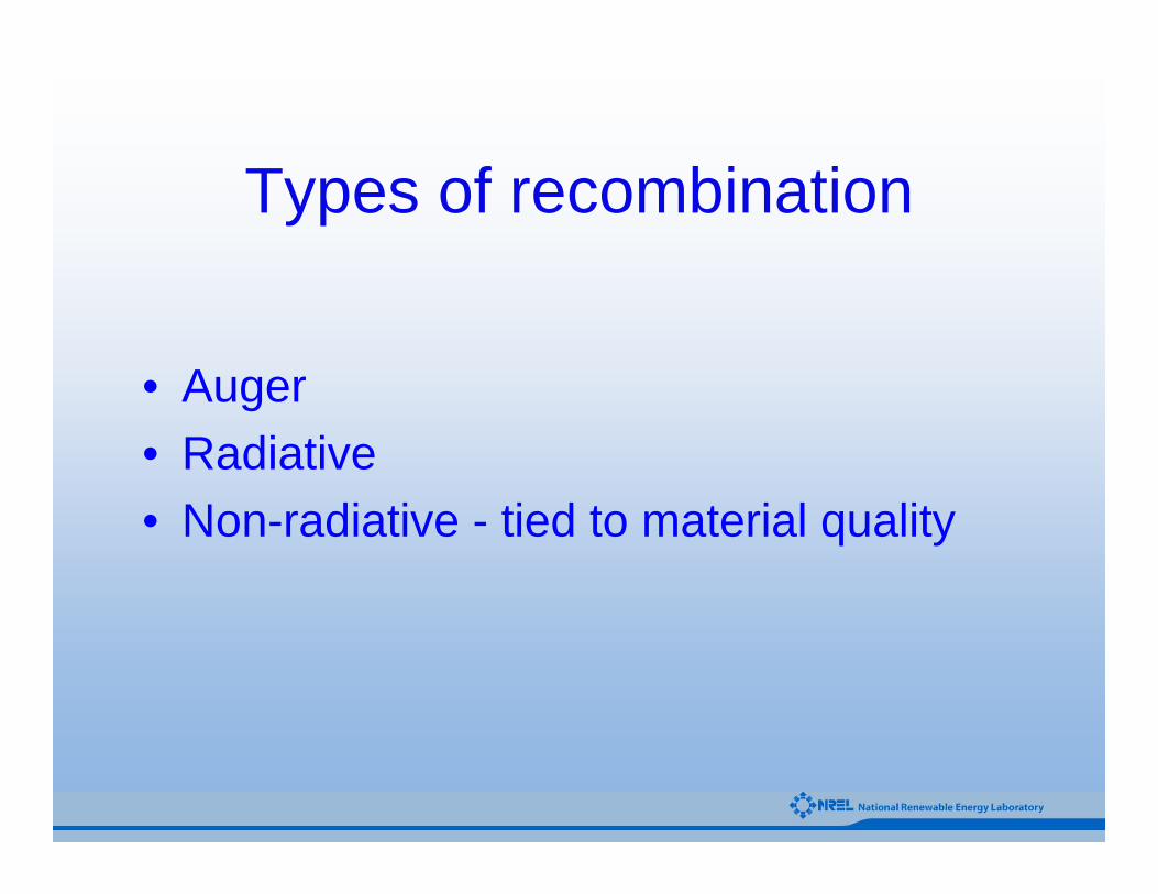
Types of recombination
• Auger• Radiative • Non-radiative - tied to material quality
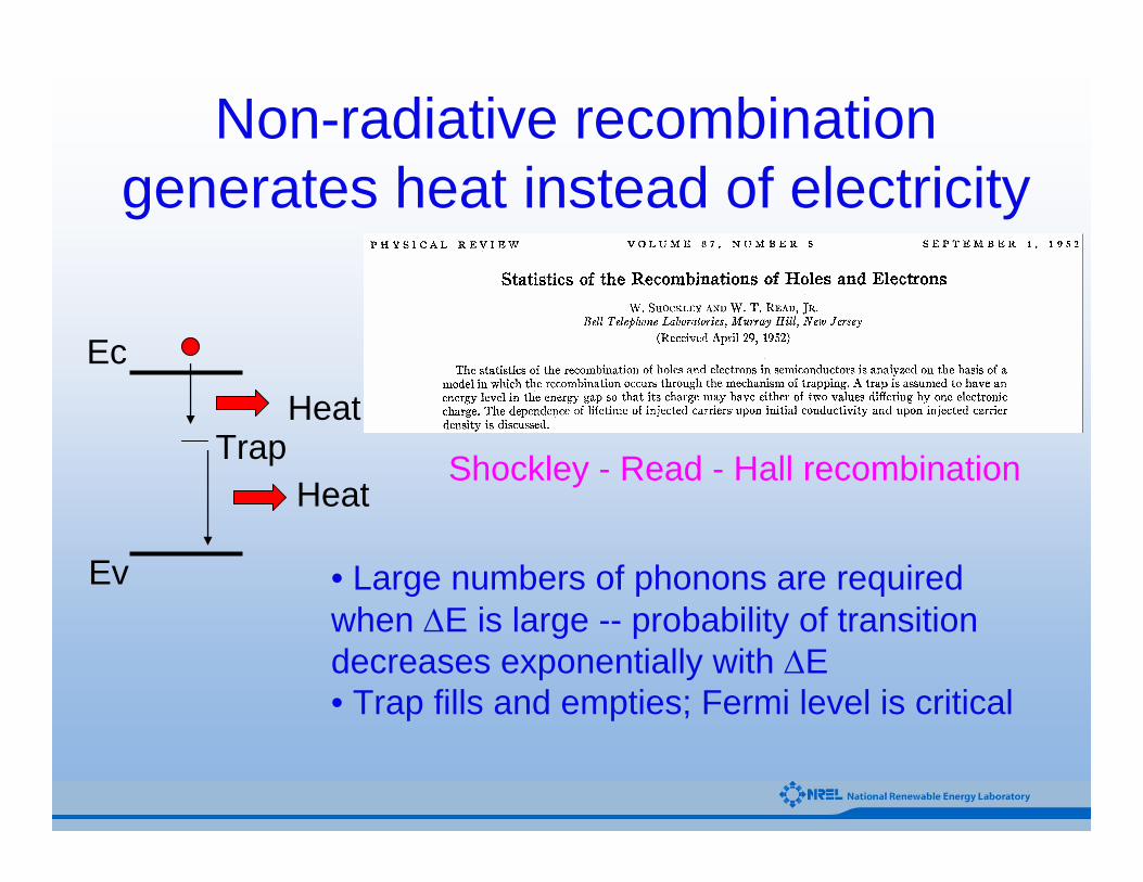
Non-radiative recombination generates heat instead of electricity
Heat
Shockley - Read - Hall recombination
• Large numbers of phonons are required when ΔE is large -- probability of transition decreases exponentially with ΔE• Trap fills and empties; Fermi level is critical
Ec
Ev
TrapHeat
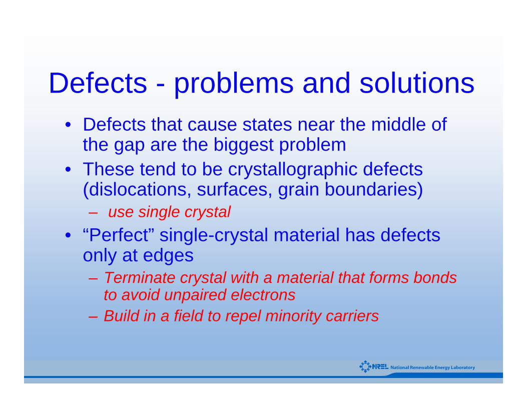
Defects - problems and solutions• Defects that cause states near the middle of
the gap are the biggest problem• These tend to be crystallographic defects
(dislocations, surfaces, grain boundaries)– use single crystal
• “Perfect” single-crystal material has defects only at edges– Terminate crystal with a material that forms bonds
to avoid unpaired electrons– Build in a field to repel minority carriers
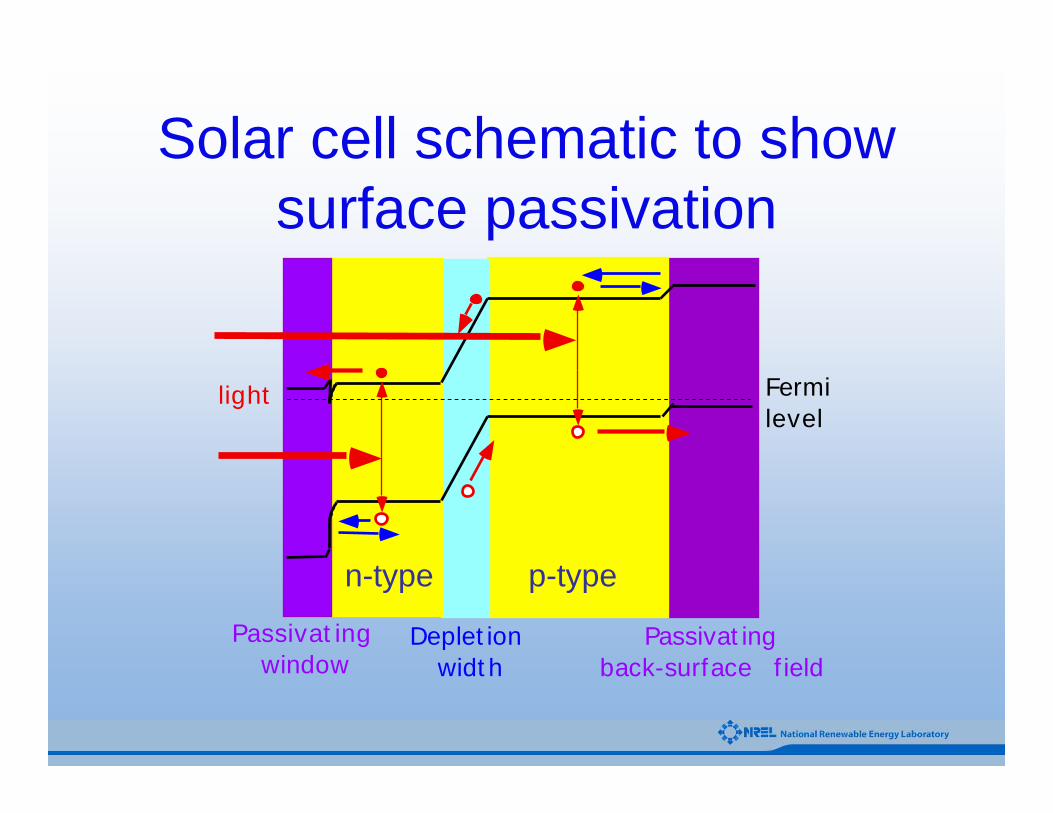
Solar cell schematic to show surface passivation
Fermilevel
Passivat ingwindow
Deplet ionwidt h
Passivat ingback-surface f ield
light
n-type p-type
Summary about high efficiency
• High efficiency cell makes rest of system more valuable
• Minimize non-radiative recombination– Use single crystal– “Get rid of” surfaces with passivating layers
• With these ground rules, how do we combine materials? - Lots of research opportunities
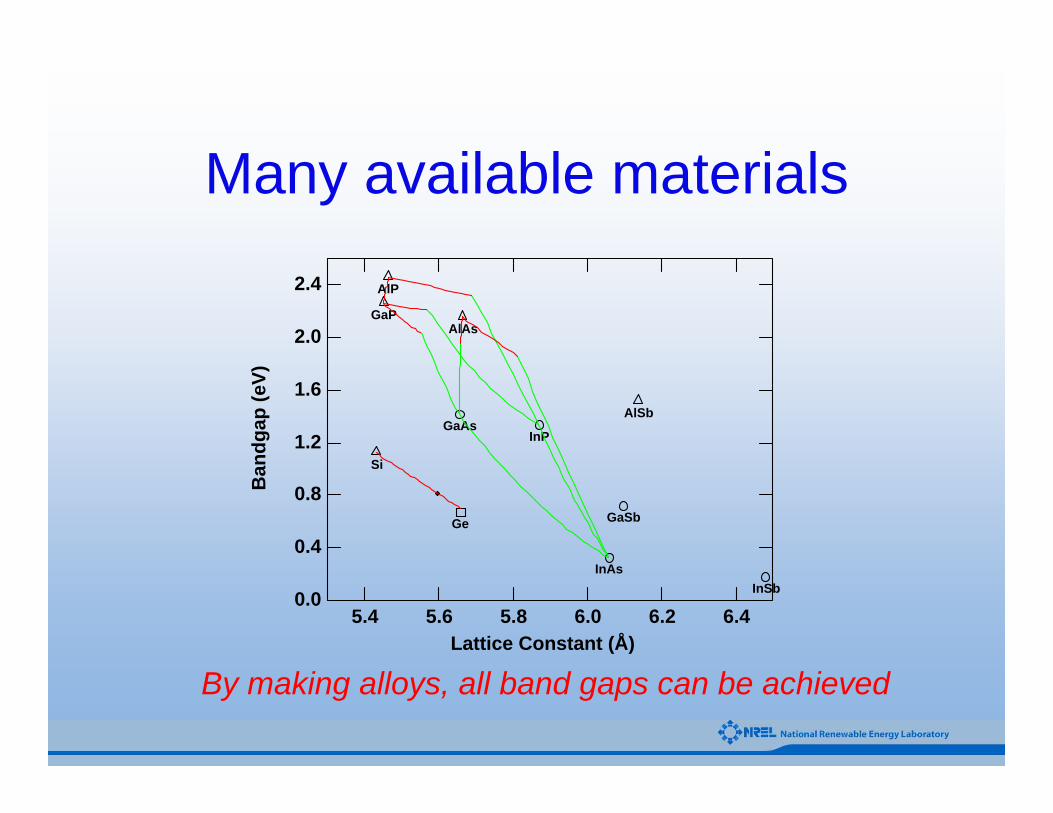
Many available materials
By making alloys, all band gaps can be achieved
2.4
2.0
1.6
1.2
0.8
0.4
0.0
Ban
dgap
(eV)
6.46.26.05.85.65.4Lattice Constant (Å)
AlP
AlAs
AlSb
GaP
GaAs
GaSb
InP
InAsInSb
Ge
Si
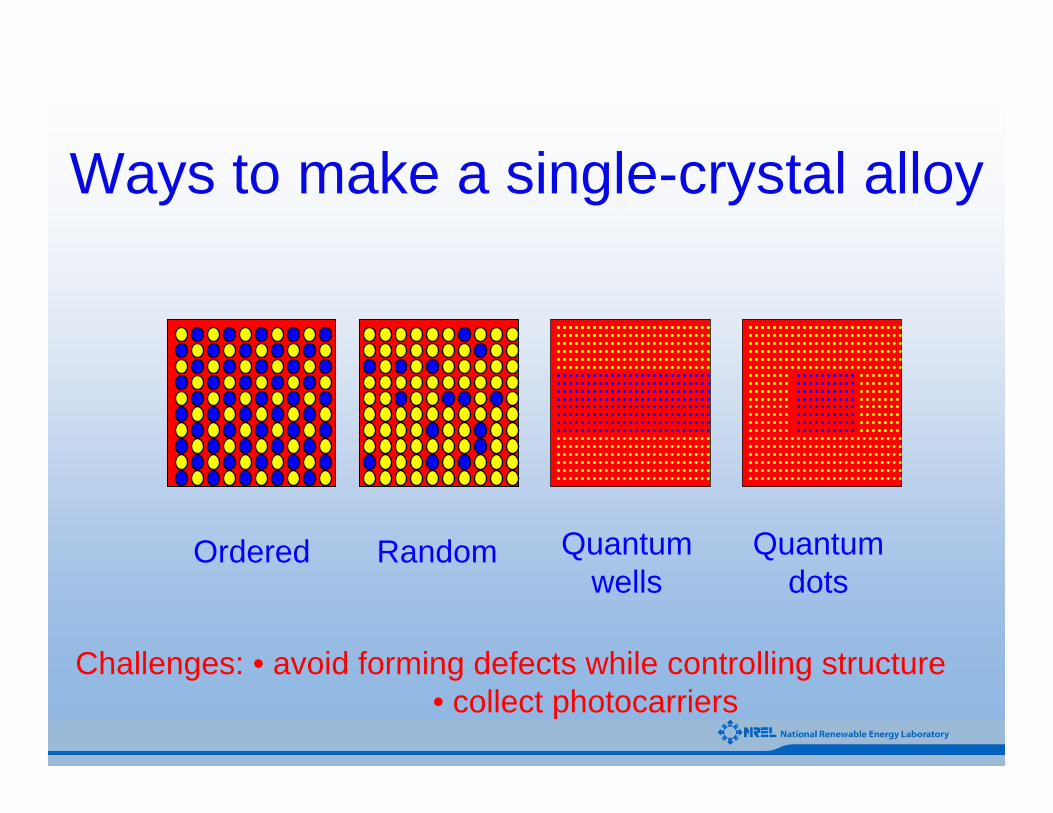
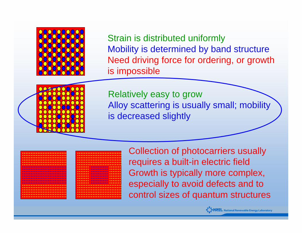
Ways to make a single-crystal alloy
Ordered Random Quantumwells
Quantumdots
Challenges: • avoid forming defects while controlling structure • collect photocarriers
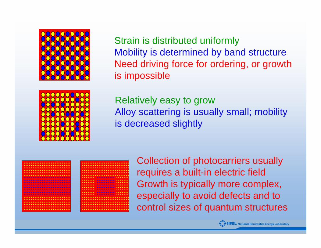
Strain is distributed uniformlyMobility is determined by band structureNeed driving force for ordering, or growth is impossible
Relatively easy to growAlloy scattering is usually small; mobility is decreased slightly
Collection of photocarriers usually requires a built-in electric fieldGrowth is typically more complex, especially to avoid defects and to control sizes of quantum structures
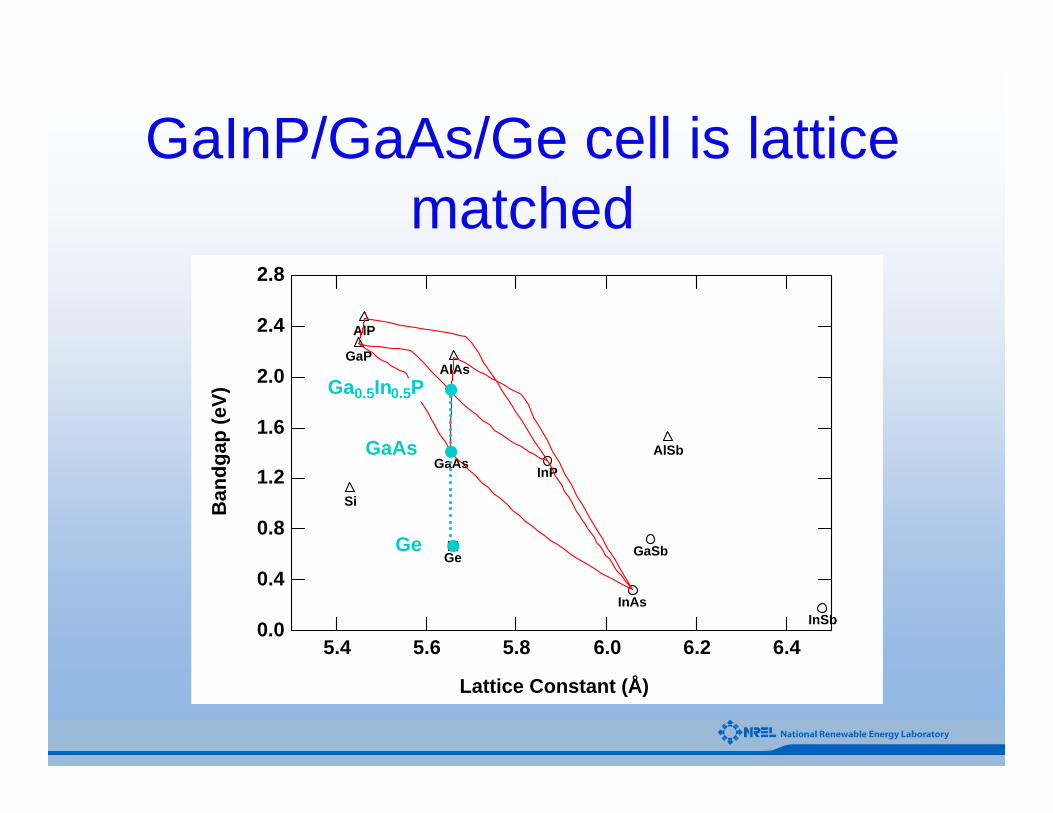
GaInP/GaAs/Ge cell is lattice matched
2.8
2.4
2.0
1.6
1.2
0.8
0.4
0.0
Ban
dgap
(eV)
6.46.26.05.85.65.4
Lattice Constant (Å)
AlP
AlAs
AlSb
GaP
GaAs
GaSb
InP
InAsInSb
Ge
Si
Ga0.5In0.5P
GaAs
Ge
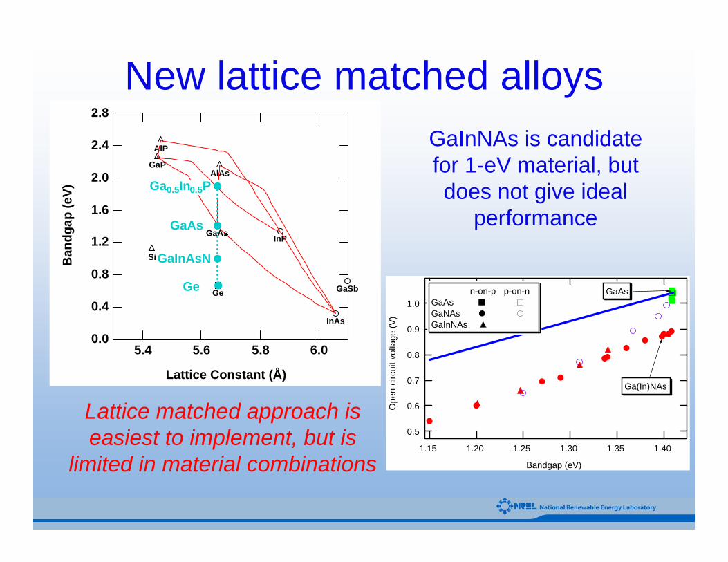
1.0
0.9
0.8
0.7
0.6
0.5
Ope
n-ci
rcui
t vol
tage
(V)
1.401.351.301.251.201.15
Bandgap (eV)
GaAs
Ga(In)NAs
n-on-p p-on-nGaAs GaNAs GaInNAs
New lattice matched alloysGaInNAs is candidate for 1-eV material, but does not give ideal
performance
Lattice matched approach is easiest to implement, but is
limited in material combinations
2.8
2.4
2.0
1.6
1.2
0.8
0.4
0.0
Ban
dgap
(eV)
6.05.85.65.4
Lattice Constant (Å)
AlP
AlAsGaP
GaAs
GaSb
InP
InAs
Ge
Si
Ga0.5In0.5P
GaAs
Ge
GaInAsN
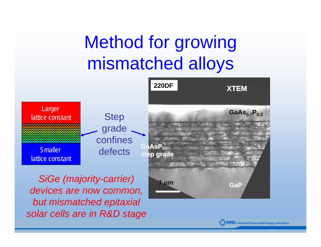
Method for growing mismatched alloys
1 1 µµmm
GaAsP GaAsP step gradestep grade
220DF
GaAsGaAs0.70.7PP0.30.3
GaPGaP
XTEMXTEM
Largerlattice constant
Smallerlattice constant
Stepgrade
confines defects
SiGe (majority-carrier) devices are now common, but mismatched epitaxial
solar cells are in R&D stage
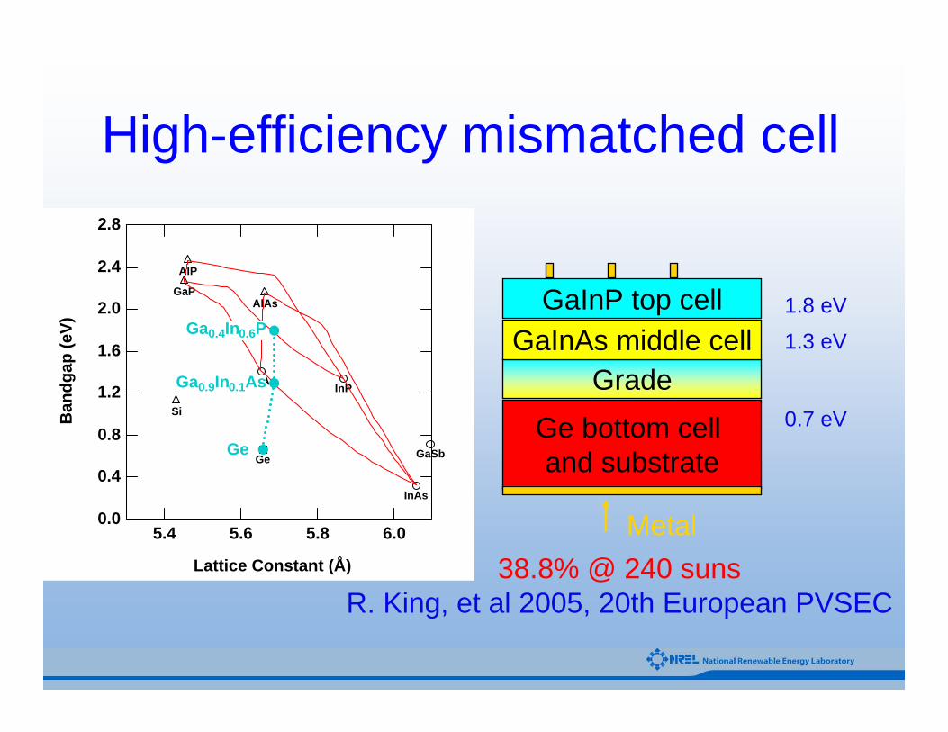
High-efficiency mismatched cell
Ge bottom cell and substrate
GradeGaInAs middle cell
GaInP top cell
Metal38.8% @ 240 suns
R. King, et al 2005, 20th European PVSEC
1.8 eV
1.3 eV
0.7 eV
2.8
2.4
2.0
1.6
1.2
0.8
0.4
0.0
Ban
dgap
(eV)
6.05.85.65.4
Lattice Constant (Å)
AlP
AlAsGaP
GaAs
GaSb
InP
InAs
Ge
Si
Ga0.4In0.6P
Ga0.9In0.1As
Ge
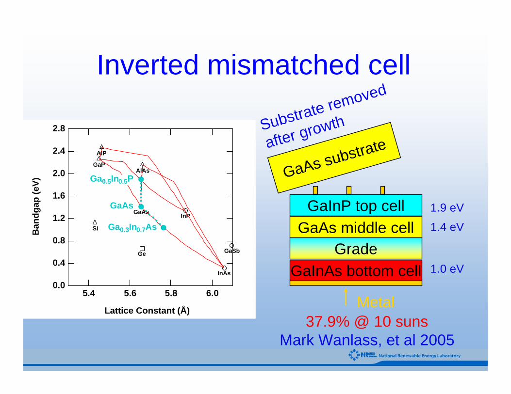
Inverted mismatched cell
GaInAs bottom cellGrade
GaAs middle cellGaInP top cell
Metal
GaAs substrateSubstrate removed
after growth
37.9% @ 10 sunsMark Wanlass, et al 2005
1.9 eV
1.4 eV
1.0 eV
2.8
2.4
2.0
1.6
1.2
0.8
0.4
0.0
Ban
dgap
(eV)
6.05.85.65.4
Lattice Constant (Å)
AlP
AlAsGaP
GaAs
GaSb
InP
InAs
Ge
Si
Ga0.5In0.5P
GaAs
Ga0.3In0.7As
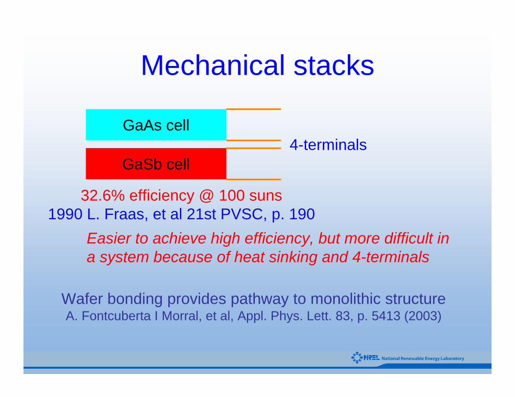
Mechanical stacks
32.6% efficiency @ 100 suns1990 L. Fraas, et al 21st PVSC, p. 190
GaAs cell
GaSb cell4-terminals
Easier to achieve high efficiency, but more difficult in a system because of heat sinking and 4-terminals
Wafer bonding provides pathway to monolithic structureA. Fontcuberta I Morral, et al, Appl. Phys. Lett. 83, p. 5413 (2003)
Summary• Photovoltaic industry is growing > 40%/year• High efficiency cells may help the solar industry
grow even faster• Detailed balance provides upper bound (>60%)
for efficiencies, assuming ideal materials• Single-crystal solar cells have achieved the
highest efficiencies: 39%• Higher efficiencies will be achieved when ways
are found to integrate materials while retaininghigh crystal quality
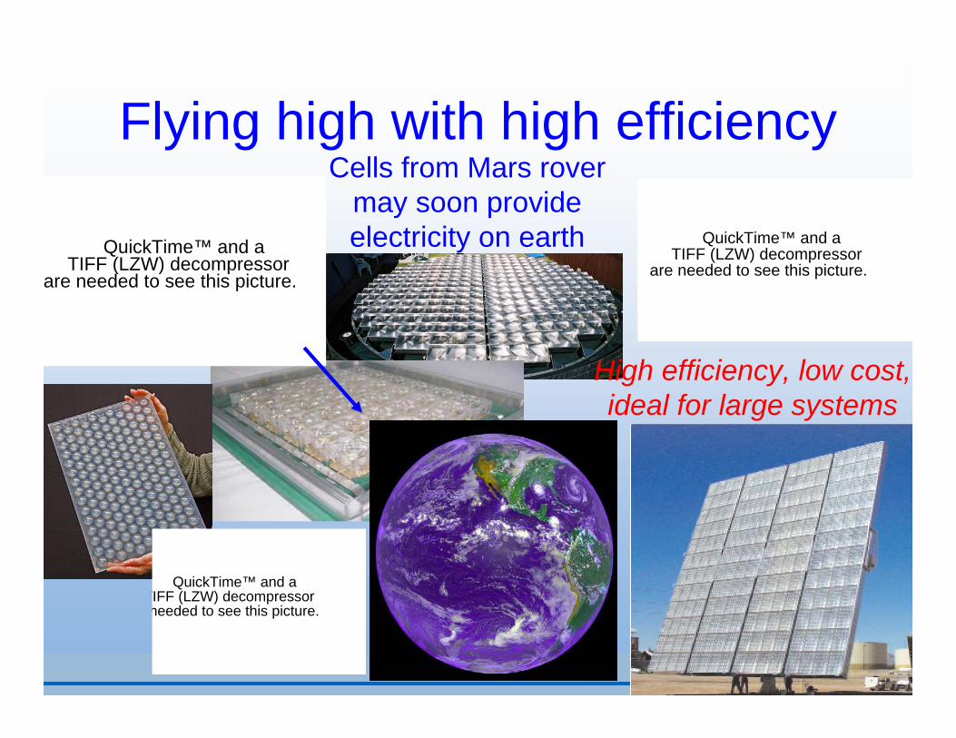
Flying high with high efficiencyCells from Mars rover
may soon provide electricity on earthQuickTime™ and a
TIFF (LZW) decompressorare needed to see this picture.
QuickTime™ and aTIFF (LZW) decompressor
are needed to see this picture.
High efficiency, low cost,ideal for large systems
QuickTime™ and aTIFF (LZW) decompressorneeded to see this picture.