gf14lpp-xl ams reference flow for finfet technology · gf14lpp-xl ams reference flow for finfet...
TRANSCRIPT

GF14LPP-XL AMS Reference Flow for FINFET Technology
Rajashekhar Chimmalagi – Design Methodology
April 5th 2016

Agenda
GLOBALFOUNDRIES 2
FinFET & FinFET Challenges
GF Reference Flows
Ref Flow Design
1
2
3
Ref Flow Modules 4
Summary 5

REVENUE
Company Highlights
GLOBALFOUNDRIES 3
East Fishkill
Singapore
Dresden Malta
Burlington
300mm
200K Wafers/Mo
200mm
133K Wafers/Mo
MORE THAN
FAB LOCATIONS FAB CAPACITY
~6B* 25,000 Patents &
Applications
2nd Largest Foundry
Trusted Foundry
*Based upon analysts’ estimates
250
Customers
18,000
Employees

Global Manufacturing Capacity: ~7M Wafers/Yr*
GLOBALFOUNDRIES 4
28nm, ≤ 14nm 45nm–22nm 180nm–40nm 350nm–90nm 90nm–22nm
TECHNOLOGY
CAPACITY IN WAFERS/MONTH
Singapore Dresden, Germany
Malta, New York
East Fishkill, New York
Burlington, Vermont
14,000 (300mm) 60,000 (300mm) 68,000 (300mm) 93,000 (200mm)
Up to 60,000 (300mm) 40,000 (200mm)
*200mm Equivalents

GLOBALFOUNDRIES 5
FinFET & FinFET Challenges
GF Reference Flows
Ref Flow Design
1
2
3
Ref Flow Modules 4
Summary 5

End of Bulk CMOS Scaling ? ?? • Planar CMOS is hitting hard scaling limits at 20nm
Shorter gates need higher doping to control leakage Higher VT at given leakage Degraded mobility Increased junction leakage Increased variation
Source Drain
Gat
e
Halo
Improved gate control of the channel requires less channel doping Lower VT at given leakage Higher mobility Lower variation Much Higher drive in the same
area foot-print [2*h+L]
Planar FET FinFET
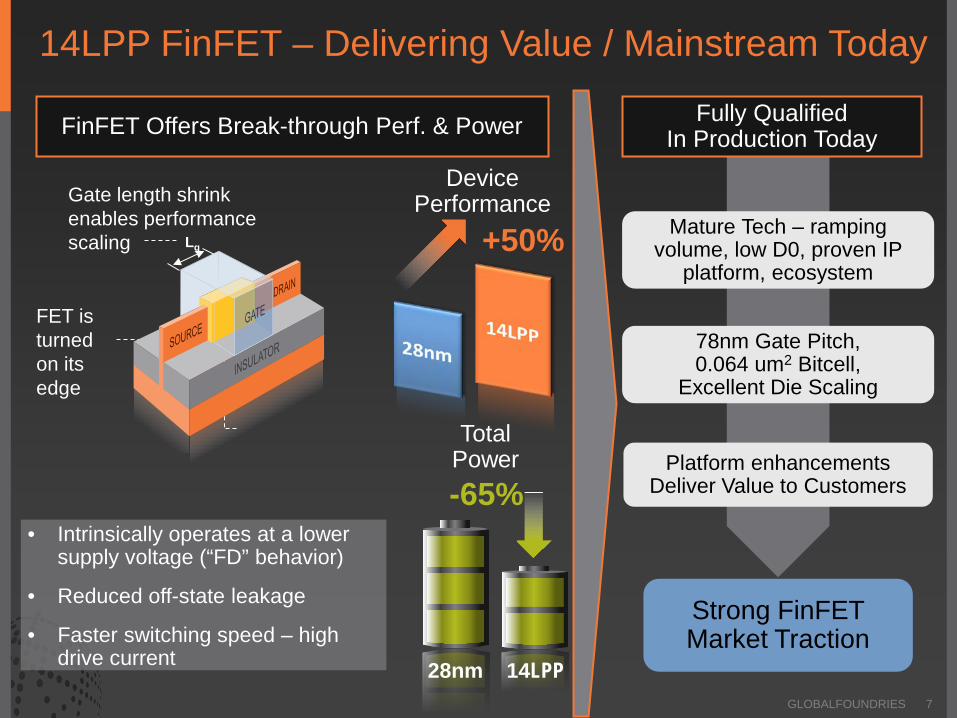
Gate length shrink enables performance scaling
Lg
14LPP FinFET – Delivering Value / Mainstream Today
GLOBALFOUNDRIES 7
• Intrinsically operates at a lower supply voltage (“FD” behavior)
• Reduced off-state leakage
• Faster switching speed – high drive current
Lg
Gate length shrink enables performance scaling
FET is turned on its edge
Device Performance
Total Power
28nm
14LPP
+50%
-65%
FinFET Offers Break-through Perf. & Power
Mature Tech – ramping volume, low D0, proven IP
platform, ecosystem
78nm Gate Pitch, 0.064 um2 Bitcell,
Excellent Die Scaling
Platform enhancements Deliver Value to Customers
Strong FinFET Market Traction
Fully Qualified In Production Today

FinFET Design Challenges
• Electrical / Circuit Challenges – Quantized width, function of number of fins
• Tuning of drive strength with number of fins
• Parasitic Challenges
– 3D structure => change in computation of parasitics – MOL extraction – Increased gate capacitance
• Miller effect magnifies this increase
GLOBALFOUNDRIES 8
Substrate
Source
C2 CA
Gate
C1 V0_CO
C3
C5
Fin
Fin
Drain C4
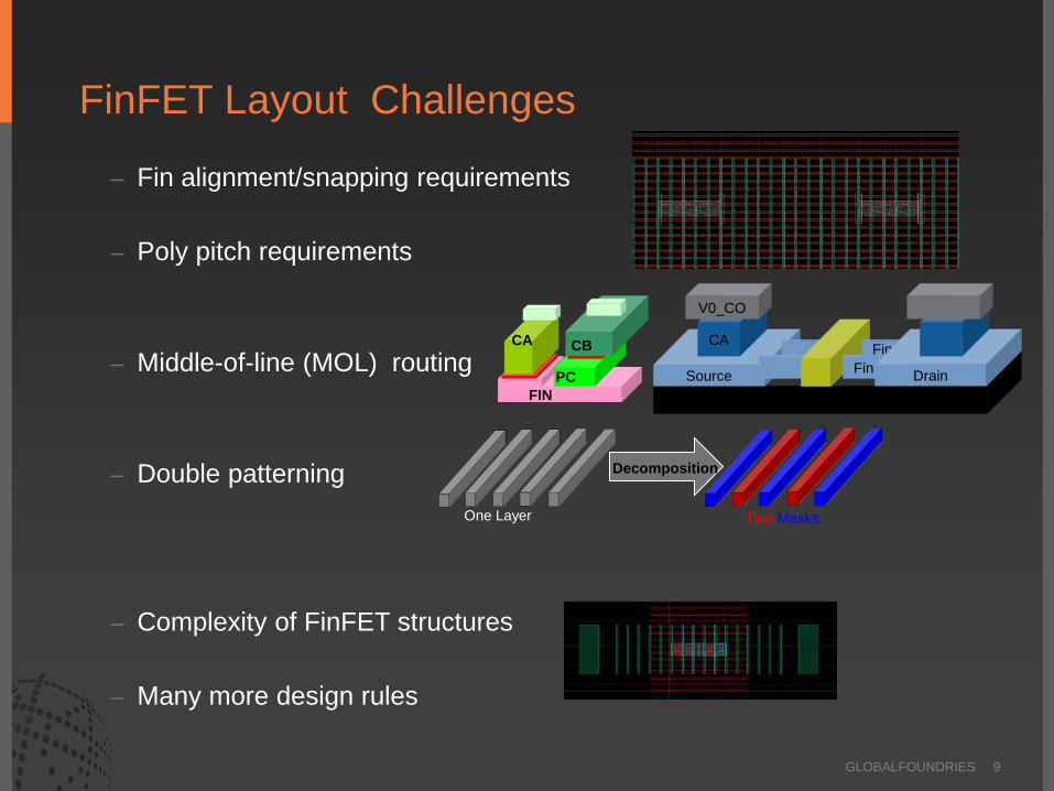
FinFET Layout Challenges
– Fin alignment/snapping requirements
– Poly pitch requirements
– Middle-of-line (MOL) routing
– Double patterning
– Complexity of FinFET structures
– Many more design rules
GLOBALFOUNDRIES 9
PC FIN
CB CA
One Layer Two Masks
Decomposition
Substrate Source
CA
Gate
V0_CO
Fin Fin
Drain

Moving from Planar to FinFET Planar FinFET Continuous Width of Transistor Discrete or Quantized Widths
Width is the Diffusion Width Width defined by number of fins
No snapping requirement Fins snapping is required
Fewer DRs, less complex device structures
More DRs, more complex device structures
GLOBALFOUNDRIES 10
3-D finFET technology: Etch uniformity requirement Fixed fin thickness/height,
quantized widths All device fins need to be
aligned to a certain spacing

Using Double Patterning to Overcome Lithographic Challenges
• Mx shape spacing are now so small that current light sources cannot print them reliably
• Solution is to split the dense shapes into two masks, each with more sparse shapes
• This process of splitting a single layer into two masks is called double patterning
GLOBALFOUNDRIES Confidential 11
One Layer Two Masks
Decomposition
Colorless Shapes (M1_drawing)
Mask1 Shapes (M1_E1)
Mask2 Shapes (M1_E2)
Mask1 & Mask2 Shapes (M1_e1, M1_e2)
GLOBALFOUNDRIES 12
Design Challenges at Advanced Nodes
GF Reference Flows
Ref Flow Design
1
2
3
Ref Flow Modules 4
Summary 5
Design Challenges at Advanced Nodes
• Design challenges at shrinking dimensions – Increased performance variation – More pronounced parasitic effects – Layout dependent effects – Explosion of design rules – Yield/defect density
• Need new methodologies and flows to tackle them!
GLOBALFOUNDRIES 13

Purpose of Reference Flow • Provide methodologies and
best practices for AMS designs using GLOBALFOUNDRIES processes
• Demonstrate GLOBALFOUNDRIES PDK differentiating features and their effective utilization
• Demonstrate the development of a working design from specification to final physical verification
• Provide a guided approach to our tool suites and foundry process
GLOBALFOUNDRIES 14
Design Flow
s & Methodologies
PDK
IP
EDA Tools
• Ensure our PDKs, EDA tools and third-party libs work together at design-level

Features of the Reference Flow
GLOBALFOUNDRIES 15
Flow steps are presented as modules
Modules are executable and independent from one another
Results are available as reference Enables check for correct
PDK and flow installation
Scripted whenever applicable Allows reuse by customer
Documented in detail Clear instructions guide user
through each step
This image cannot currently be displayed.
This image cannot currently be displayed.
This image cannot currently be displayed.

GLOBALFOUNDRIES 16
GF Reference Flows
Ref Flow Design
2
3
Summary 5
FinFET & FinFET Challenges 1
Ref Flow Modules 4

Design Overview
• Delay Controlled Oscillators (DCO) – DCOs are widely used in PLLs for generating clocks – DCO consists of DCO core and Bias current generator
• Specs – Oscillation frequency: 500MHz – Tuning range: 0.5GHz +/- 100MHz – Power consumption: < 25uA – Supply voltage: 1V +/- 200mV – Temperature: -40C to 150C
GLOBALFOUNDRIES 17
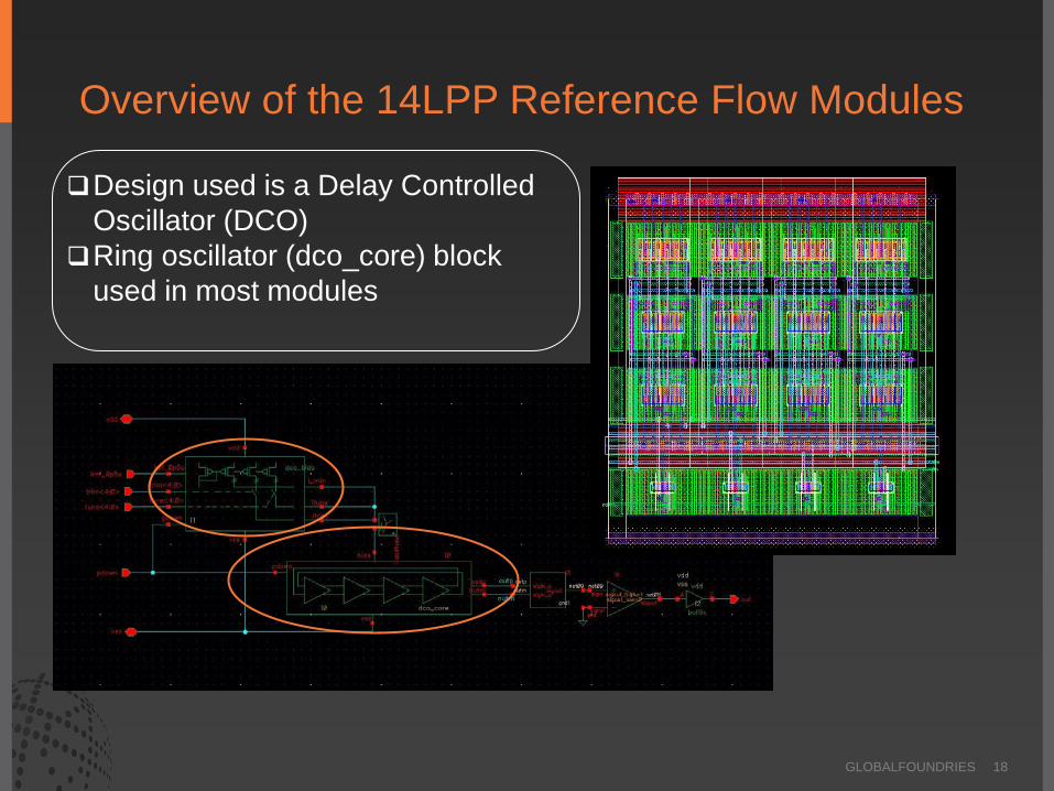
Overview of the 14LPP Reference Flow Modules
GLOBALFOUNDRIES 18
Design used is a Delay Controlled Oscillator (DCO)
Ring oscillator (dco_core) block used in most modules

GLOBALFOUNDRIES 19
GF Reference Flows
Ref Flow Design
2
3
Summary 5
Design Challenges at Advanced Nodes 1
Ref Flow Modules 4

14LPP AMS Ref Flow – Modules
GLOBALFOUNDRIES 20
Streamout Netlist
GDS / Netlist Generation
PhyVerif DRC / LVS / DPT
PEX PEX
Module 1 DCO Circuit Design
Module 2 Unit Cell Partial Layout
Module 3 Unit Cell Device Placement Re-simulation
Module 4 Unit Cell Routing
Module 5 Unit Extraction Cell Sign-Off
Module 6 DCO Assembly Routing
Other Modules
Module 7 DCO Sign-Off
Cadence Modules

Module 1: DCO Circuit Design Objective Functional Design, Characterization over PVT and Exploring LLE, WPE in 14nm FinFET
GLOBALFOUNDRIES 21
Schematic Creation Delay cell, DCO
Statistical variation MonteCarlo Analysis
DCO Characterization over PVTs
Exploring LLE, WPE and Assessing potential mismatch to
post-layout simulation results
Set layout constraints and Hand over to back-end team
Design Tasks
Devices Lib
PDK Features
Models with corners
Models with statistical info
BSIM-CMG with LLE param WPE approximation added
to BSIM-CMG core ADEXL/MMSIM
Tool
ADEXL/MMSIM
ADEXL/MMSIM
VSE
CMS
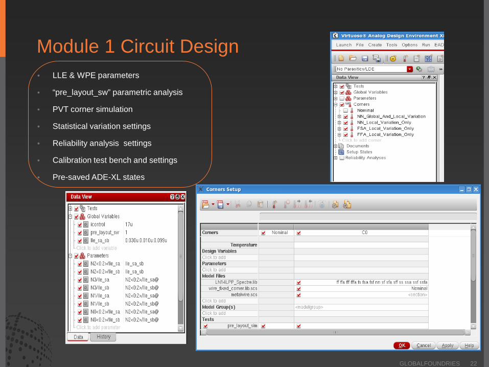
Module 1 Circuit Design
GLOBALFOUNDRIES 22
• LLE & WPE parameters
• “pre_layout_sw” parametric analysis
• PVT corner simulation
• Statistical variation settings
• Reliability analysis settings
• Calibration test bench and settings
• Pre-saved ADE-XL states
Tool
PDK Features
Design Task
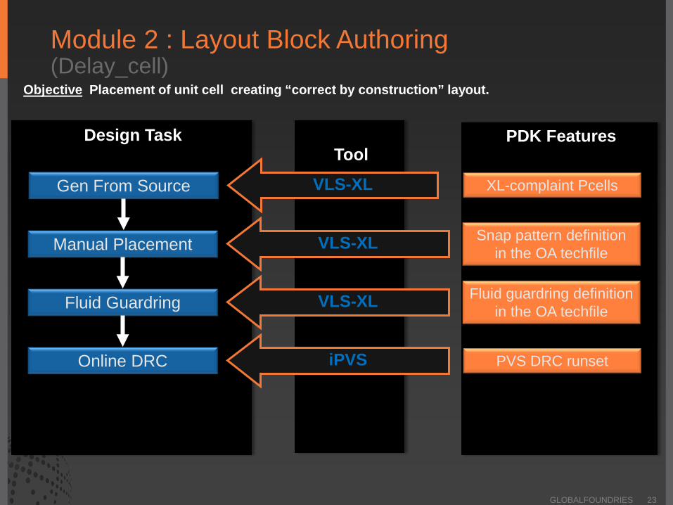
Module 2 : Layout Block Authoring (Delay_cell)
Objective Placement of unit cell creating “correct by construction” layout.
GLOBALFOUNDRIES 23
Gen From Source
Manual Placement
Fluid Guardring
Online DRC
VLS-XL
VLS-XL
VLS-XL
iPVS
XL-complaint Pcells
Snap pattern definition in the OA techfile
Fluid guardring definition in the OA techfile
PVS DRC runset
Module 2: Layout Block Authoring
• Unit cell placement – Brief explanation of important FinFet pCell features , CDFs and settings – Generate from source to create connectivity based layout – Template cell aids easy placement – Snapping and how FinFets are snapped automatically – Connectivity less abutment with dummy poly – Fluid guard ring to create p and n taps – iPVS with presets to run DRC on the fly
GLOBALFOUNDRIES 24

Module 2 Layout Block Authoring
GLOBALFOUNDRIES 25
(1) Place template (2) Place instances (3) Complete routing

Objective Investigate influence of placed FinFet devices RC Parasitics impact
GLOBALFOUNDRIES 26
Device Placement
Device Parasitics Pre-routing Simulation
RC Extraction
Placement sign-off for routing
Design Tasks
XL-compliant Pcells
PDK Features
PVS runset , QRC Setup
Tool
PVS/QRC
VLS-XL
ADE-XL/MMSIM
Module 3: Block Placement Validation
Models

Module 3: Block Placement Validation
• The device parasitic have greater influence
• Placement validation before doing the routing
• “Add LVS Labels” util to create labels on pCell inst terms
• LVS with virtual connectivity and save the SVDB
• RCX with “extview.il” proc to create extracted view
• ADE-XL simulation and analyze the placement
• Variable “delaycell_diff_view” run the corner simulation
GLOBALFOUNDRIES 27

Tool/ Feature
PDK Features
Design Task
Wire Editor Routing default constraint in the OA techfile Pin to Trunk Routing
Manual wire editing
Auto routing
Net-constrained Routing
Constraint Validation Checker
Wire Editor
Wire Editor
Space-based Router
Routing default constraint in the OA techfile
Routing default constraint in the OA techfile
Routing default constraint in the OA techfile
PVS CV
Objective Routing of the design with the features of VLS-XL.
GLOBALFOUNDRIES 28
Module 4 : Block Layout Routing
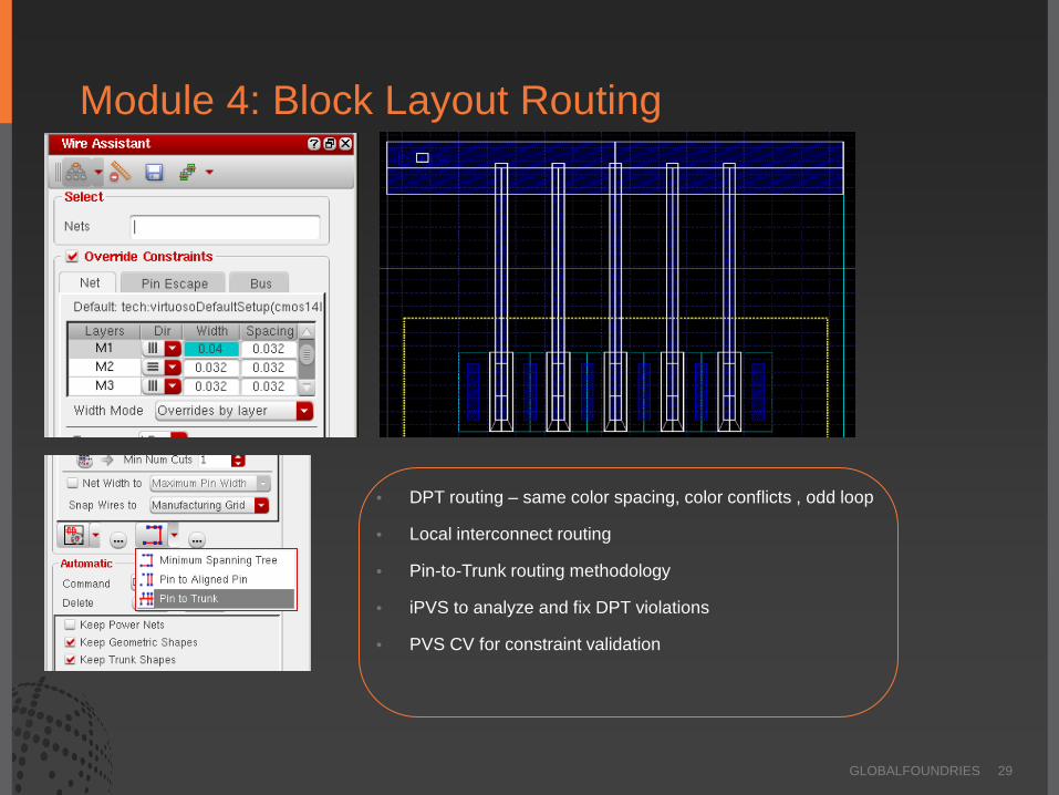
Module 4: Block Layout Routing
GLOBALFOUNDRIES 29
• DPT routing – same color spacing, color conflicts , odd loop
• Local interconnect routing
• Pin-to-Trunk routing methodology
• iPVS to analyze and fix DPT violations
• PVS CV for constraint validation
Tool/ Feature
PDK Features
Design Task
PVS PVS ruledecks for OpenAccess
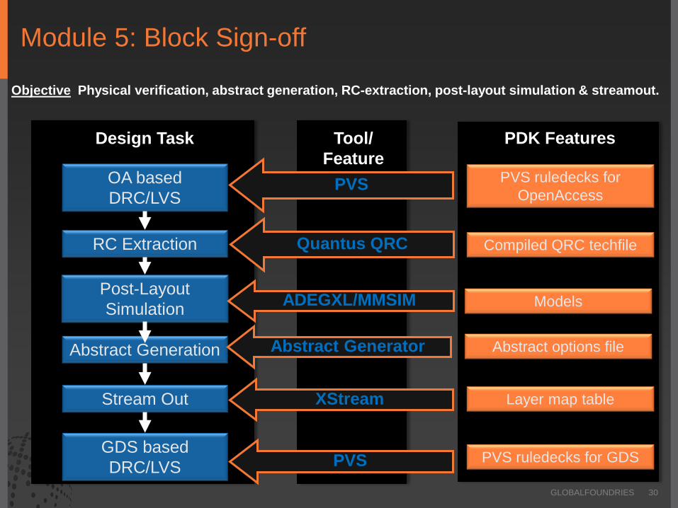
Module 5: Block Sign-off
Objective Physical verification, abstract generation, RC-extraction, post-layout simulation & streamout.
GLOBALFOUNDRIES 30
OA based DRC/LVS
GDS based DRC/LVS
RC Extraction
Stream Out
Abstract Generation Abstract Generator Abstract options file
Layer map table XStream
PVS PVS ruledecks for GDS
Quantus QRC Compiled QRC techfile
Post-Layout Simulation ADEGXL/MMSIM Models
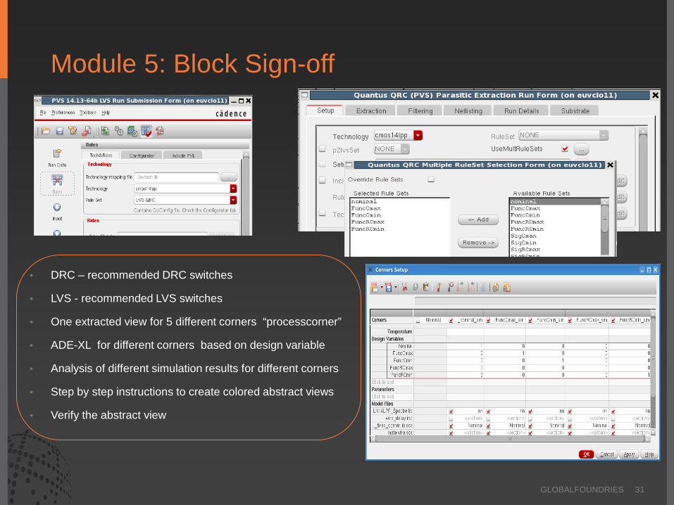
Module 5: Block Sign-off
GLOBALFOUNDRIES 31
• DRC – recommended DRC switches
• LVS - recommended LVS switches
• One extracted view for 5 different corners “processcorner”
• ADE-XL for different corners based on design variable
• Analysis of different simulation results for different corners
• Step by step instructions to create colored abstract views
• Verify the abstract view

Tool/ Feature
PDK Features
Design Task
Gen From Source
Placement Refinement
DRC LVS
VLS-XL
VLS-XL
VSR / Wire Editor
ViPVS
Routing default constraint in the OA techfile
PVS DRC runset
Module 6 : Design Layout Assembly Objective Assembly of all the unit cells , routing and DPT sign-off.
GLOBALFOUNDRIES 32
Routing
DPT Sign-off
PVS PVS Rule Deck
Snap pattern definition in the OA techfile
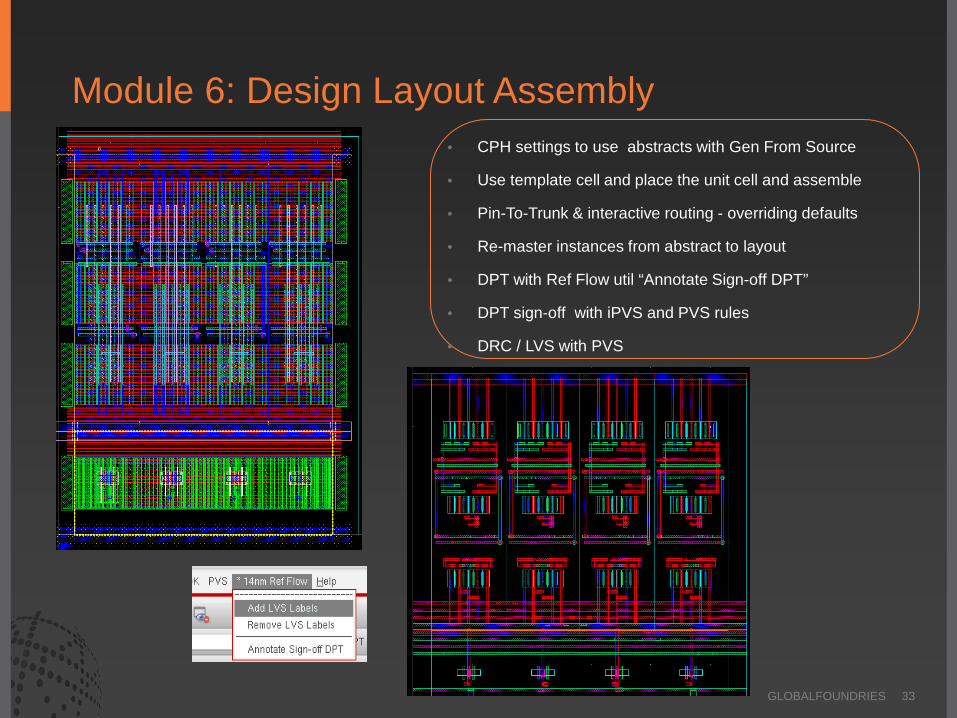
Module 6: Design Layout Assembly
GLOBALFOUNDRIES 33
• CPH settings to use abstracts with Gen From Source
• Use template cell and place the unit cell and assemble
• Pin-To-Trunk & interactive routing - overriding defaults
• Re-master instances from abstract to layout
• DPT with Ref Flow util “Annotate Sign-off DPT”
• DPT sign-off with iPVS and PVS rules
• DRC / LVS with PVS

Module 7: Design Sign-Off
Objective: Full design implementation physical verification , streaming out to GDS & abstract creation .
GLOBALFOUNDRIES 34
Tool/ Feature
PDK Features
Design Task
PVS OA based DRC/LVS
GDS based DRC/LVS
RC Extraction Post-layout SIM
Stream Out Layer map table XStream
PVS PVS ruledecks for GDS
Quantus QRC MMSIM
Compiled QRC techfile Models (BSIM-CMG)
Abstract Generation Abstract Generator Abstract options file
PVS ruledecks for OpenAccess

Design Task
GDSII / CDL creation
DP Generation & DRC
DP Merge
preDP DRC
Fully colored DRC LVS
Objective DPT generation , merging and sign-off on fully colored GDS.
GLOBALFOUNDRIES 35
Module : PhyVerif
• Demonstration of DRC LVS.
• Scripts for Netlist and Colored GDS
• Scripted runs for DPT
• DRC LVS recommended switches
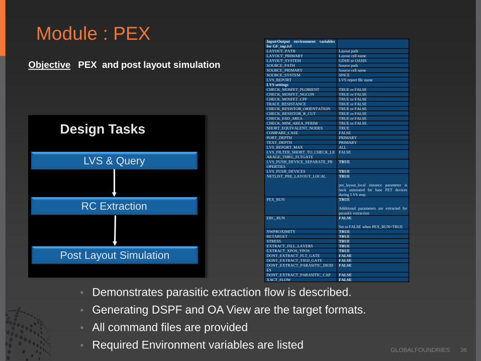
Objective PEX and post layout simulation
GLOBALFOUNDRIES 36
LVS & Query
Post Layout Simulation
RC Extraction
Design Tasks
Module : PEX Input/Output environment variables for GF_top.tvf
LAYOUT_PATH Layout path LAYOUT_PRIMARY Layout cell name LAYOUT_SYSTEM GDSII or OASIS SOURCE_PATH Source path SOURCE_PRIMARY Source cell name SOURCE_SYSTEM SPICE LVS_REPORT LVS report file name LVS settings CHECK_MOSFET_PLORIENT TRUE or FALSE CHECK_MOSFET_NGCON TRUE or FALSE CHECK_MOSFET_CPP TRUE or FALSE TRACE_RESISTANCE TRUE or FALSE CHECK_RESISTOR_ORIENTATION TRUE or FALSE CHECK_RESISTOR_R_CUT TRUE or FALSE CHECK_ESD_AREA TRUE or FALSE CHECK_MIM_AREA_PERIM TRUE or FALSE SHORT_EQUIVALENT_NODES TRUE COMPARE_CASE FALSE PORT_DEPTH PRIMARY TEXT_DEPTH PRIMARY LVS_REPORT_MAX ALL LVS_FILTER_SHORT_TO_CHECK_LEAKAGE_THRU_FLTGATE
FALSE
LVS_PUSH_DEVICE_SEPARATE_PROPERTIES
TRUE
LVS_PUSH_DEVICES TRUE NETLIST_PRE_LAYOUT_LOCAL TRUE
pre_layout_local instance parameter is back annotated for base FET devices during LVS step.
PEX_RUN TRUE
Additional parameters are extracted for parasitic extraction
ERC_RUN FALSE
Set to FALSE when PEX_RUN=TRUE NWPROXIMITY TRUE RETARGET TRUE STRESS TRUE EXTRACT_FILL_LAYERS TRUE EXTRACT_XPOS_YPOS TRUE DONT_EXTRACT_FLT_GATE FALSE DONT_EXTRACT_TIED_GATE FALSE DONT_EXTRACT_PARASITIC_DIODES
FALSE
DONT_EXTRACT_PARASITIC_CAP FALSE XACT_FLOW FALSE
• Demonstrates parasitic extraction flow is described. • Generating DSPF and OA View are the target formats. • All command files are provided • Required Environment variables are listed

Parasitic Extraction
Post-Layout Functional Verification
14LPP Reference Flow Modules
GLOBALFOUNDRIES 37
Pre-Layout Functional Verification
Accelerated Custom Layout
MSOA Interoperability
Physical Verification
Voltus-FI
Virtuoso/EDI*
Schematic-XL/Layout-XL
ADE-XL/MMSIM
Voltus-FI*
Quantus QRC
ADE-XL/MMSIM
PVS
* Planned for V2

GLOBALFOUNDRIES Reference Flows How to get them?
GLOBALFOUNDRIES 38

GLOBALFOUNDRIES 39
GF Reference Flows
Ref Flow Design
2
3
Ref Flow Modules 4
Design Challenges at Advanced Nodes 1
Summary 5

Summary
• 14LPP Modules are well documented with step by step instructions
• FinFET features are highlighted nicely
• Use of “template” cell for easy placement
• Provided utils will improve the AMS design methodology
• Phase II will have MSOA, EM/IR modules
GLOBALFOUNDRIES 40

Acknowledgements
• GLOBALFOUNDRIES : – Richard Trihy , Venkat Ramasubramanian, Hendrik Mau, Rais Huda,
Sascha Hoefer, Winnie Ng, Tim Miller
• CADENCE : – Louis Thiam , John Pierce, Aryoko Prakoso, Tran Hoang
GLOBALFOUNDRIES Confidential 41

Disclaimer The information contained herein [is confidential and] is the property of GLOBALFOUNDRIES and/or its licensors. This document is for informational purposes only, is current only as of the date of publication and is subject to change by GLOBALFOUNDRIES at any time without notice. GLOBALFOUNDRIES, the GLOBALFOUNDRIES logo and combinations thereof are trademarks of GLOBALFOUNDRIES Inc. in the United States and/or other jurisdictions. Other product or service names are for identification purposes only and may be trademarks or service marks of their respective owners. © GLOBALFOUNDRIES Inc. 2016. Unless otherwise indicated, all rights reserved. Do not copy or redistribute except as expressly permitted by GLOBALFOUNDRIES.
Thank you