fundamentals of microelectronicstorlak/courses/ee3311/lectures/ch06updated.pdf · fundamentals of...
TRANSCRIPT
11/13/2010
1
1
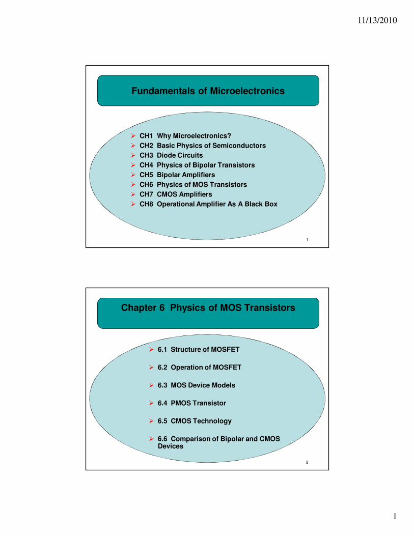
Fundamentals of Microelectronics
� CH1 Why Microelectronics?
� CH2 Basic Physics of Semiconductors
� CH3 Diode Circuits
� CH4 Physics of Bipolar Transistors
� CH5 Bipolar Amplifiers
� CH6 Physics of MOS Transistors
� CH7 CMOS Amplifiers
� CH8 Operational Amplifier As A Black Box
2
Chapter 6 Physics of MOS Transistors
� 6.1 Structure of MOSFET
� 6.2 Operation of MOSFET
� 6.3 MOS Device Models
� 6.4 PMOS Transistor
� 6.5 CMOS Technology
� 6.6 Comparison of Bipolar and CMOS Devices
11/13/2010
2
CH 6 Physics of MOS Transistors 3
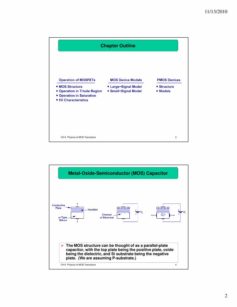
Chapter Outline
CH 6 Physics of MOS Transistors 4
Metal-Oxide-Semiconductor (MOS) Capacitor
� The MOS structure can be thought of as a parallel-plate capacitor, with the top plate being the positive plate, oxide being the dielectric, and Si substrate being the negative plate. (We are assuming P-substrate.)
11/13/2010
3
CH 6 Physics of MOS Transistors 5
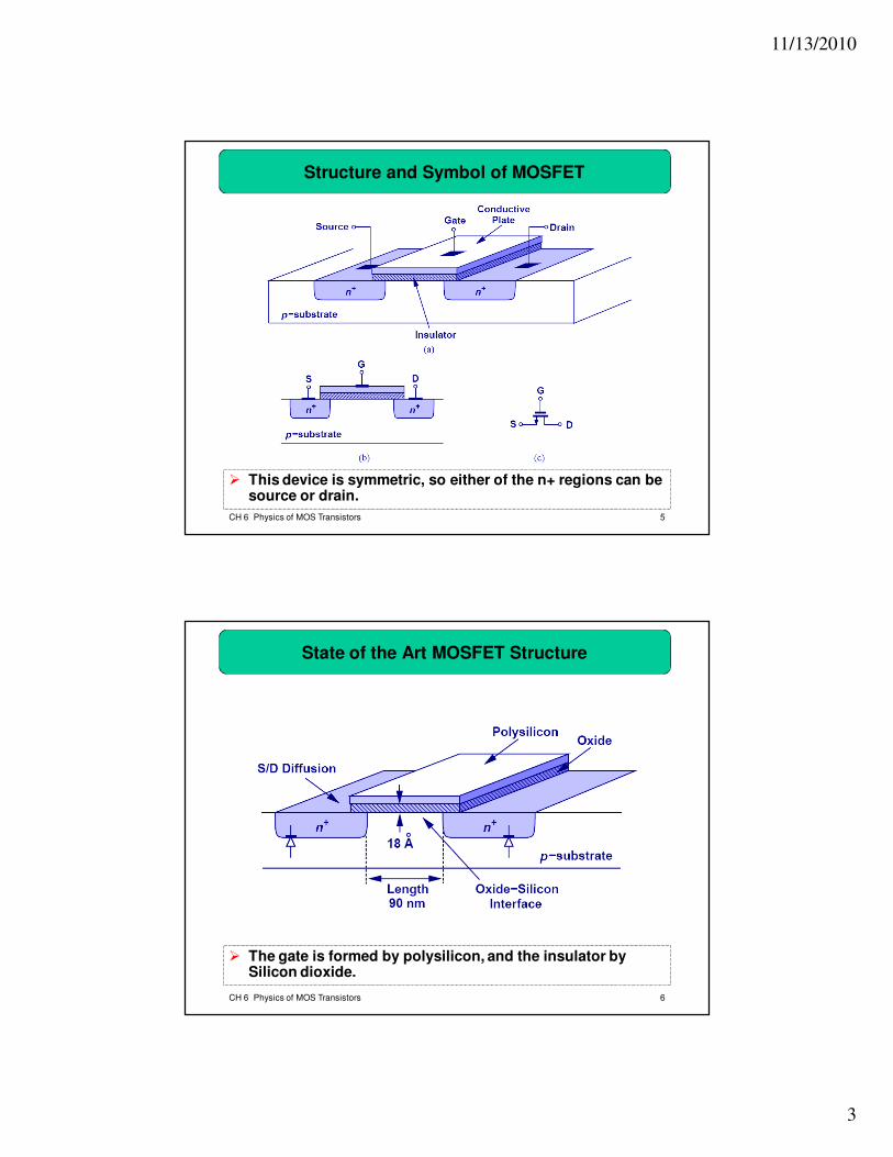
Structure and Symbol of MOSFET
� This device is symmetric, so either of the n+ regions can be source or drain.
CH 6 Physics of MOS Transistors 6
State of the Art MOSFET Structure
� The gate is formed by polysilicon, and the insulator by Silicon dioxide.
11/13/2010
4
CH 6 Physics of MOS Transistors 7
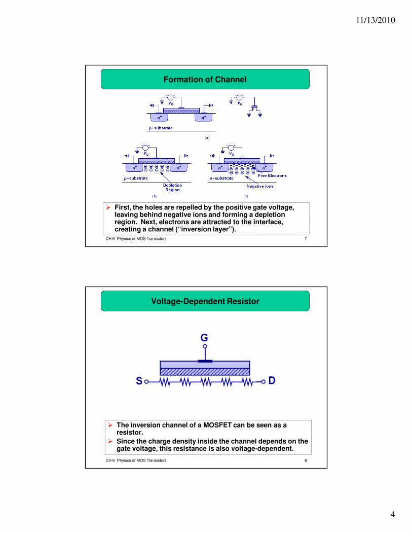
Formation of Channel
� First, the holes are repelled by the positive gate voltage, leaving behind negative ions and forming a depletion region. Next, electrons are attracted to the interface, creating a channel (“inversion layer”).
CH 6 Physics of MOS Transistors 8
Voltage-Dependent Resistor
� The inversion channel of a MOSFET can be seen as a resistor.
� Since the charge density inside the channel depends on the gate voltage, this resistance is also voltage-dependent.
11/13/2010
5
CH 6 Physics of MOS Transistors 9
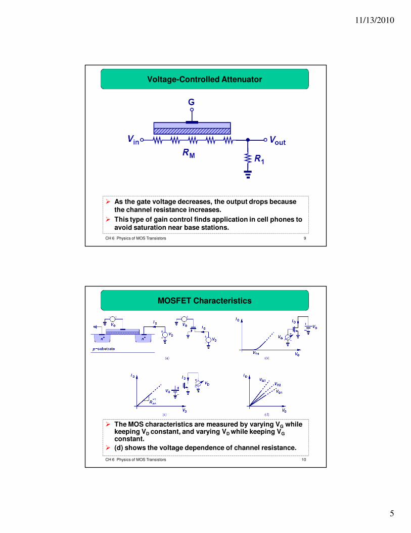
Voltage-Controlled Attenuator
� As the gate voltage decreases, the output drops because the channel resistance increases.
� This type of gain control finds application in cell phones to avoid saturation near base stations.
CH 6 Physics of MOS Transistors 10
MOSFET Characteristics
� The MOS characteristics are measured by varying VG while keeping VD constant, and varying VD while keeping VG
constant.
� (d) shows the voltage dependence of channel resistance.
11/13/2010
6
CH 6 Physics of MOS Transistors 11
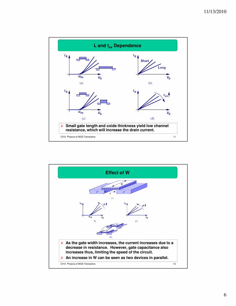
L and tox Dependence
� Small gate length and oxide thickness yield low channel resistance, which will increase the drain current.
CH 6 Physics of MOS Transistors 12
Effect of W
� As the gate width increases, the current increases due to a decrease in resistance. However, gate capacitance also increases thus, limiting the speed of the circuit.
� An increase in W can be seen as two devices in parallel.
11/13/2010
7
CH 6 Physics of MOS Transistors 13
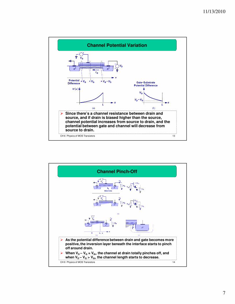
Channel Potential Variation
� Since there’s a channel resistance between drain and source, and if drain is biased higher than the source, channel potential increases from source to drain, and the potential between gate and channel will decrease from source to drain.
CH 6 Physics of MOS Transistors 14
Channel Pinch-Off
� As the potential difference between drain and gate becomes more positive, the inversion layer beneath the interface starts to pinch off around drain.
� When VD – VG = Vth, the channel at drain totally pinches off, and when VD – VG > Vth, the channel length starts to decrease.
11/13/2010
8
CH 6 Physics of MOS Transistors 15
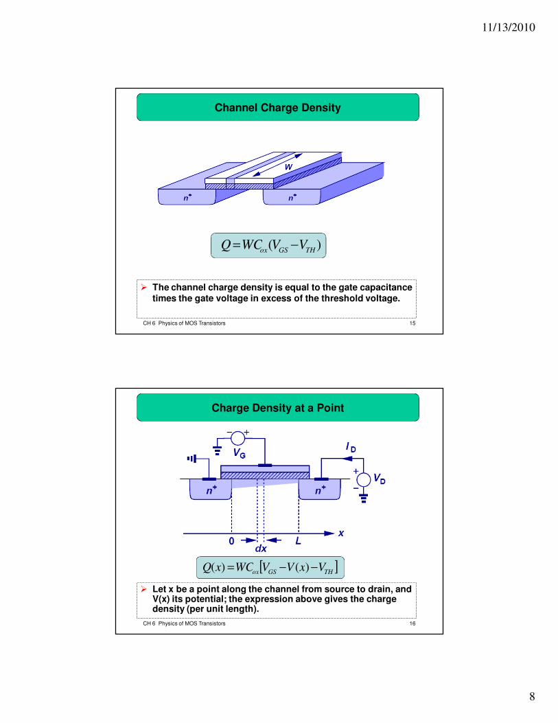
Channel Charge Density
� The channel charge density is equal to the gate capacitance times the gate voltage in excess of the threshold voltage.
)(THGSox
VVWCQ −=
CH 6 Physics of MOS Transistors 16
Charge Density at a Point
� Let x be a point along the channel from source to drain, and V(x) its potential; the expression above gives the charge density (per unit length).
[ ]THGSox
VxVVWCxQ −−= )()(
11/13/2010
9
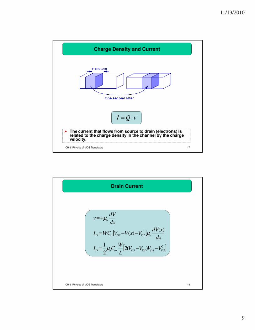
CH 6 Physics of MOS Transistors 17
Charge Density and Current
� The current that flows from source to drain (electrons) is related to the charge density in the channel by the charge velocity.
vQI ⋅=
CH 6 Physics of MOS Transistors 18
Drain Current
[ ]
[ ]2)(2
2
1
)()(
DSDSTHGSoxnD
nTHGSoxD
n
VVVVL
WCI
dx
xdVVxVVWCI
dx
dVv
−−=
−−=
+=
µ
µ
µ
11/13/2010
10
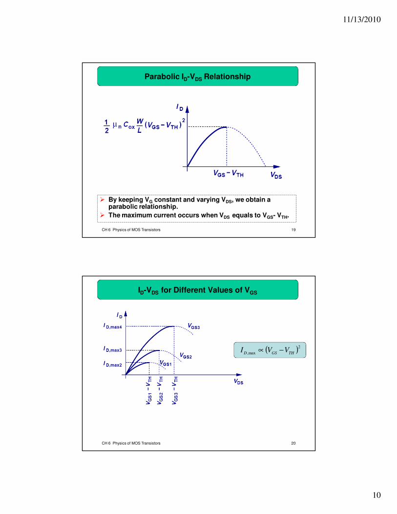
CH 6 Physics of MOS Transistors 19
Parabolic ID-VDS Relationship
� By keeping VG constant and varying VDS, we obtain a parabolic relationship.
� The maximum current occurs when VDS equals to VGS- VTH.
CH 6 Physics of MOS Transistors 20
ID-VDS for Different Values of VGS
( )2
max, THGSDVVI −∝
11/13/2010
11
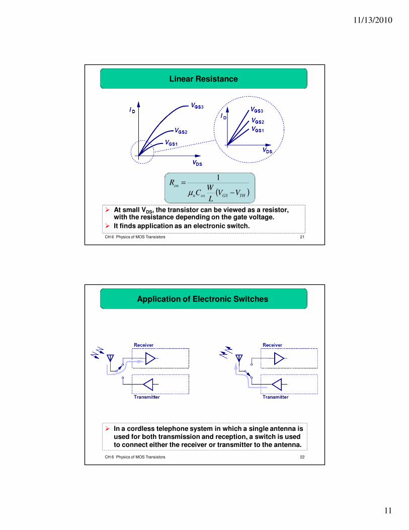
CH 6 Physics of MOS Transistors 21
Linear Resistance
� At small VDS, the transistor can be viewed as a resistor, with the resistance depending on the gate voltage.
� It finds application as an electronic switch.
( )THGSoxn
on
VVL
WC
R
−
=
µ
1
CH 6 Physics of MOS Transistors 22
Application of Electronic Switches
� In a cordless telephone system in which a single antenna is used for both transmission and reception, a switch is used to connect either the receiver or transmitter to the antenna.
11/13/2010
12
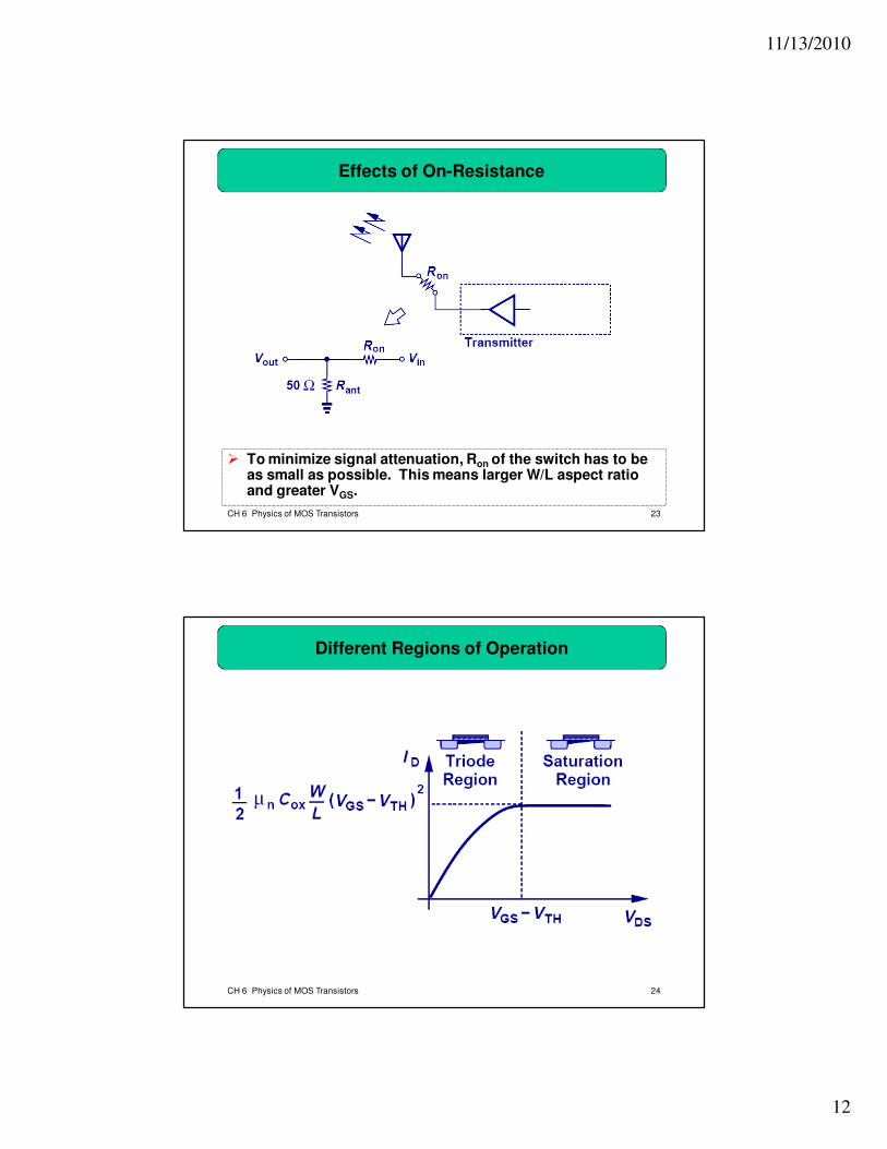
CH 6 Physics of MOS Transistors 23
Effects of On-Resistance
� To minimize signal attenuation, Ron of the switch has to be as small as possible. This means larger W/L aspect ratio and greater VGS.
CH 6 Physics of MOS Transistors 24
Different Regions of Operation
11/13/2010
13
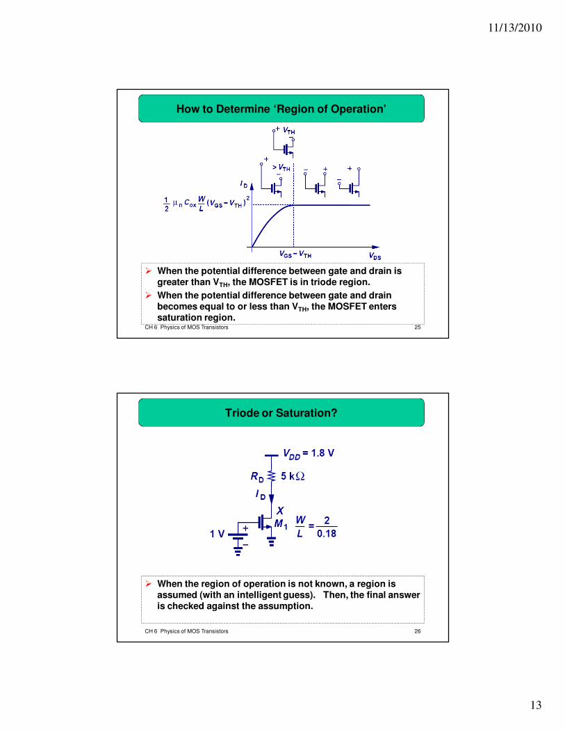
CH 6 Physics of MOS Transistors 25
How to Determine ‘Region of Operation’
� When the potential difference between gate and drain is greater than VTH, the MOSFET is in triode region.
� When the potential difference between gate and drain becomes equal to or less than VTH, the MOSFET enters saturation region.
CH 6 Physics of MOS Transistors 26
Triode or Saturation?
� When the region of operation is not known, a region is assumed (with an intelligent guess). Then, the final answer is checked against the assumption.
11/13/2010
14
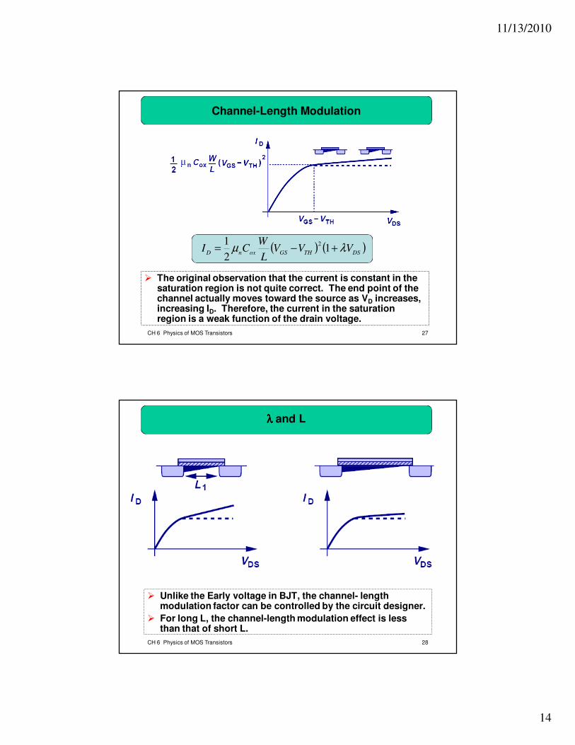
CH 6 Physics of MOS Transistors 27
Channel-Length Modulation
� The original observation that the current is constant in the saturation region is not quite correct. The end point of the channel actually moves toward the source as VD increases, increasing ID. Therefore, the current in the saturation region is a weak function of the drain voltage.
( ) ( )DSTHGSoxnD
VVVL
WCI λµ +−= 1
2
1 2
CH 6 Physics of MOS Transistors 28
λλλλ and L
� Unlike the Early voltage in BJT, the channel- length modulation factor can be controlled by the circuit designer.
� For long L, the channel-length modulation effect is less than that of short L.
11/13/2010
15
CH 6 Physics of MOS Transistors 29
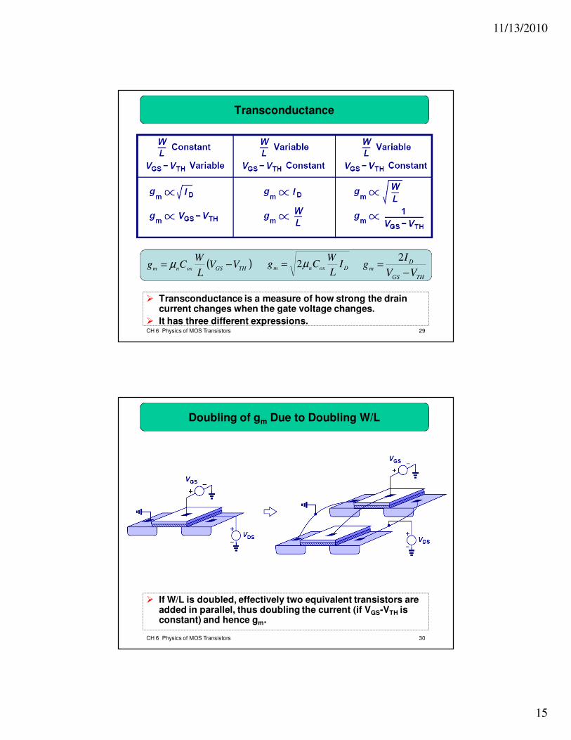
Transconductance
� Transconductance is a measure of how strong the drain current changes when the gate voltage changes.
� It has three different expressions.
( )THGSoxnm
VVL
WCg −= µ Doxnm
IL
WCg µ2=
THGS
Dm
VV
Ig
−=
2
CH 6 Physics of MOS Transistors 30
Doubling of gm Due to Doubling W/L
� If W/L is doubled, effectively two equivalent transistors are added in parallel, thus doubling the current (if VGS-VTH is constant) and hence gm.
11/13/2010
16
CH 6 Physics of MOS Transistors 31
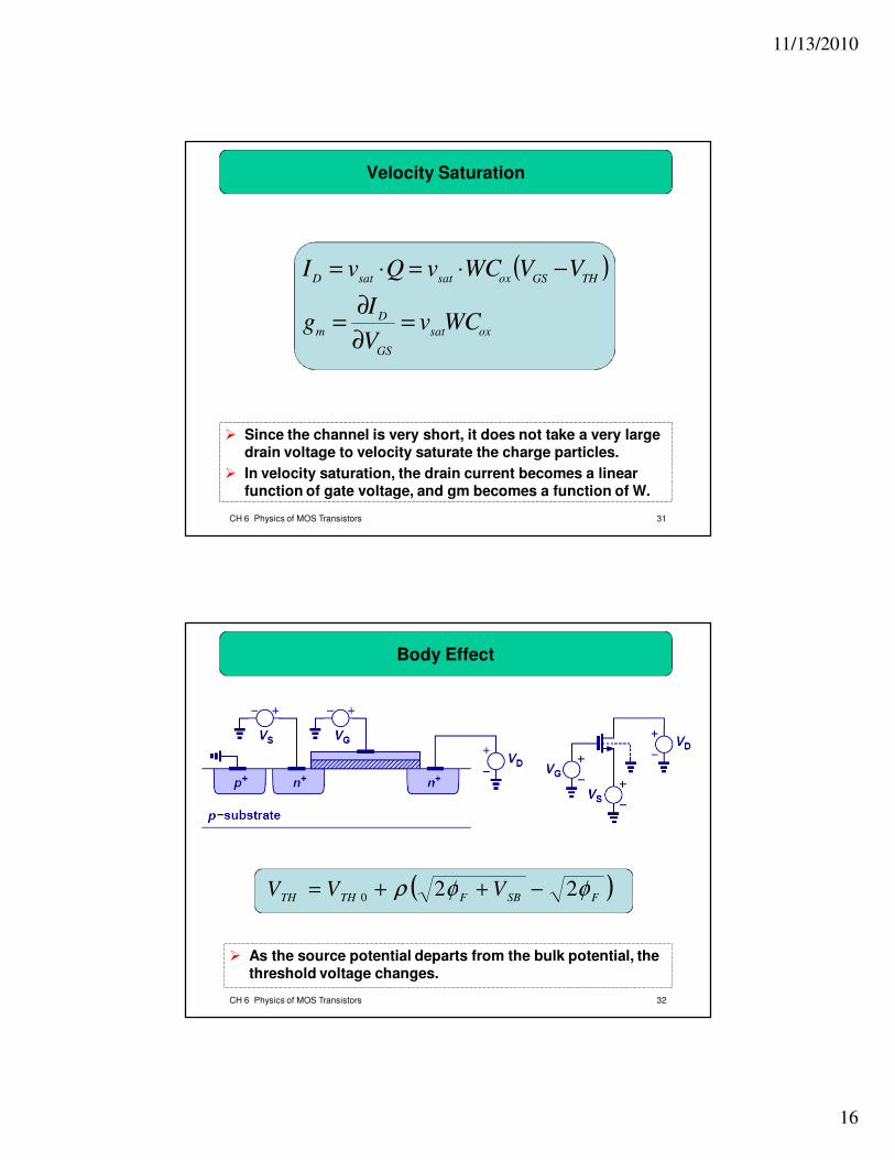
Velocity Saturation
� Since the channel is very short, it does not take a very large drain voltage to velocity saturate the charge particles.
� In velocity saturation, the drain current becomes a linear function of gate voltage, and gm becomes a function of W.
( )
oxsat
GS
D
m
THGSoxsatsatD
WCvV
Ig
VVWCvQvI
=∂
∂=
−⋅=⋅=
CH 6 Physics of MOS Transistors 32
Body Effect
� As the source potential departs from the bulk potential, the threshold voltage changes.
( )FSBFTHTH
VVV φφρ 220
−++=

11/13/2010
17
CH 6 Physics of MOS Transistors 33
Large-Signal Models
� Based on the value of VDS, MOSFET can be represented
with different large-signal models.
CH 6 Physics of MOS Transistors 34
Example: Behavior of ID with V1 as a Function
� Since V1 is connected at the source, as it increases, the current drops.
( )2
12
1THDDoxnD
VVVL
WCI −−= µ
11/13/2010
18
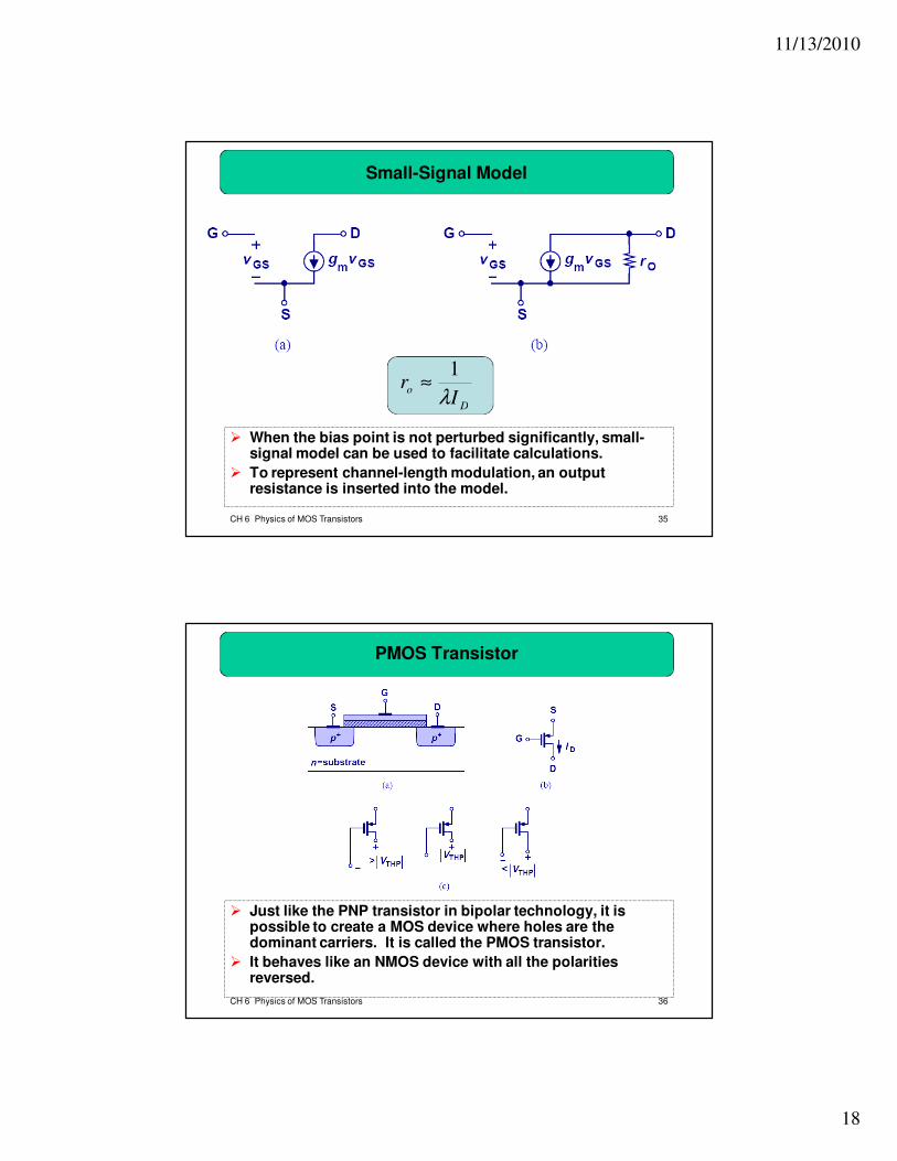
CH 6 Physics of MOS Transistors 35
Small-Signal Model
� When the bias point is not perturbed significantly, small-signal model can be used to facilitate calculations.
� To represent channel-length modulation, an output resistance is inserted into the model.
D
oI
rλ
1≈
CH 6 Physics of MOS Transistors 36
PMOS Transistor
� Just like the PNP transistor in bipolar technology, it is possible to create a MOS device where holes are the dominant carriers. It is called the PMOS transistor.
� It behaves like an NMOS device with all the polarities reversed.
11/13/2010
19
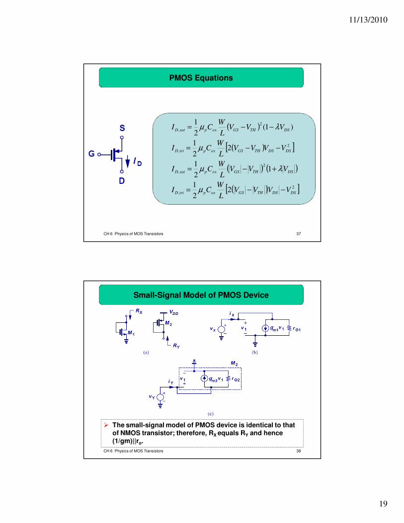
CH 6 Physics of MOS Transistors 37
PMOS Equations
( )
( )[ ]
( ) ( )
( )[ ]2
,
2
,
2
,
2
,
22
1
12
1
22
1
)1(2
1
DSDSTHGSoxptriD
DSTHGSoxpsatD
DSDSTHGSoxptriD
DSTHGSoxpsatD
VVVVL
WCI
VVVL
WCI
VVVVL
WCI
VVVL
WCI
−−=
+−=
−−=
−−=
µ
λµ
µ
λµ
CH 6 Physics of MOS Transistors 38
Small-Signal Model of PMOS Device
� The small-signal model of PMOS device is identical to that of NMOS transistor; therefore, RX equals RY and hence (1/gm)||ro.

11/13/2010
20
CH 6 Physics of MOS Transistors 39
CMOS Technology
� It possible to grow an n-well inside a p-substrate to create a technology where both NMOS and PMOS can coexist.
� It is known as CMOS, or “Complementary MOS”.
CH 6 Physics of MOS Transistors 40
Comparison of Bipolar and MOS Transistors
� Bipolar devices have a higher gm than MOSFETs for a given bias current due to its exponential IV characteristics.