frequency shift keying demodulators for low … · frequency shift keying demodulators for...
TRANSCRIPT
FREQUENCY SHIFT KEYING DEMODULATORS FOR
LOW-POWER FPGA APPLICATIONS
by
RILEY T. HARRINGTON
B.S., Kansas State University, 2011
B.S., Washburn University, 2012
A THESIS
submitted in partial fulfillment of the requirements for the degree
MASTER OF SCIENCE
Department of Electrical and Computer Engineering
College of Engineering
KANSAS STATE UNIVERSITY
Manhattan, Kansas
2017
Approved by:
Major Professor
Dr. Dwight Day

Copyright
RILEY T HARRINGTON
2017
Abstract
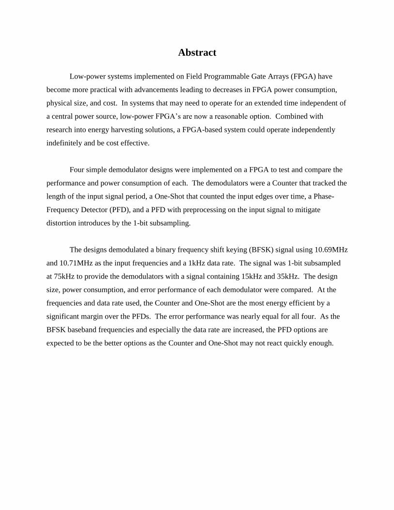
Low-power systems implemented on Field Programmable Gate Arrays (FPGA) have
become more practical with advancements leading to decreases in FPGA power consumption,
physical size, and cost. In systems that may need to operate for an extended time independent of
a central power source, low-power FPGA’s are now a reasonable option. Combined with
research into energy harvesting solutions, a FPGA-based system could operate independently
indefinitely and be cost effective.
Four simple demodulator designs were implemented on a FPGA to test and compare the
performance and power consumption of each. The demodulators were a Counter that tracked the
length of the input signal period, a One-Shot that counted the input edges over time, a Phase-
Frequency Detector (PFD), and a PFD with preprocessing on the input signal to mitigate
distortion introduces by the 1-bit subsampling.
The designs demodulated a binary frequency shift keying (BFSK) signal using 10.69MHz
and 10.71MHz as the input frequencies and a 1kHz data rate. The signal was 1-bit subsampled
at 75kHz to provide the demodulators with a signal containing 15kHz and 35kHz. The design
size, power consumption, and error performance of each demodulator were compared. At the
frequencies and data rate used, the Counter and One-Shot are the most energy efficient by a
significant margin over the PFDs. The error performance was nearly equal for all four. As the
BFSK baseband frequencies and especially the data rate are increased, the PFD options are
expected to be the better options as the Counter and One-Shot may not react quickly enough.
iv
Table of Contents
List of Figures ................................................................................................................................ vi
List of Tables ................................................................................................................................ vii
Acknowledgements ...................................................................................................................... viii
Chapter 1 - Introduction .................................................................................................................. 1
Frequency Shift Keying .............................................................................................................. 2
Demodulation Methods ............................................................................................................... 3
Chapter 2 - Sampling ...................................................................................................................... 6
Subsampling ................................................................................................................................ 8
1-bit Sampling Distortion ......................................................................................................... 12
Averaging .................................................................................................................................. 16
Chapter 3 - Demodulator Design .................................................................................................. 19
Counter ...................................................................................................................................... 19
One-Shot ................................................................................................................................... 21
Phase-Frequency Detector ........................................................................................................ 22
Phase Frequency Detector with Preprocessor ........................................................................... 26
Chapter 4 - Demodulator Comparison Tests ................................................................................ 28
Power Consumption .................................................................................................................. 28
Size of Design ....................................................................................................................... 28
Power .................................................................................................................................... 29
Error Analysis ........................................................................................................................... 29
Eye Diagram ............................................................................................................................. 32
Chapter 5 - Conclusions and Future Work ................................................................................... 33
References ..................................................................................................................................... 37
Appendix A – Hardware Design Language (HDL), Verilog Code .............................................. 39
Counter ...................................................................................................................................... 39
One-Shot ................................................................................................................................... 41
Phase Frequency Detector ........................................................................................................ 43
Phase Frequency Detector with Preprocessor ........................................................................... 44
Supporting Modules .................................................................................................................. 46
v
Edge Detector ........................................................................................................................ 46
Clock Divider ........................................................................................................................ 47
Bit Sync ................................................................................................................................. 47
Binomial Average Filter ....................................................................................................... 49
Moving Average Filter .......................................................................................................... 50
Appendix B – MATLAB Code ..................................................................................................... 53
Counter ...................................................................................................................................... 53
One-Shot ................................................................................................................................... 53
Phase Frequency Detector ........................................................................................................ 53
Phase Frequency Detector with Preprocessor ........................................................................... 55
Test Bed .................................................................................................................................... 55
Supporting Modules .................................................................................................................. 64
Error Generation ................................................................................................................... 64
Find Edges ............................................................................................................................ 68
Subsampling .......................................................................................................................... 69
Replace Zeros ........................................................................................................................ 69
Repeat Elements .................................................................................................................... 70
Averaging Filter .................................................................................................................... 70
vi
List of Figures
Figure 1-1. BFSK and Demodulated Waveforms ........................................................................... 2
Figure 1-2. Phase-Frequency Detector Circuit Model .................................................................... 5
Figure 1-3. Example PFD Inputs and Outputs ................................................................................ 5
Figure 2-1 (a-d). Signal Sample Rates ............................................................................................ 7
Figure 2-2. Signal Bandwidth Position ........................................................................................... 8
Figure 2-3. Aliasing Diagram Showing Alias Overlap ................................................................... 9
Figure 2-4 (a-d). Frequency Domain ............................................................................................ 11
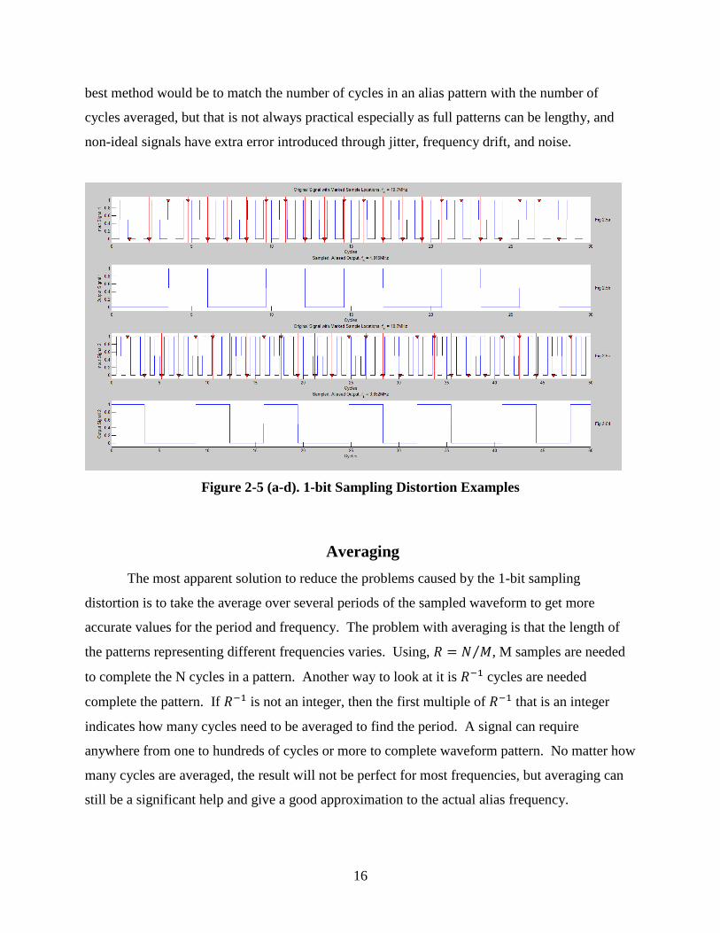
Figure 2-5 (a-d). 1-bit Sampling Distortion Examples ................................................................. 16
Figure 2-6. Period Averaging Example, R = 17/100 .................................................................... 17
Figure 2-7. MSE with No Averaging ............................................................................................ 18
Figure 2-8. MSE with Averaging 8 Periods.................................................................................. 18
Figure 3-1. Counter Demodulator Simulation .............................................................................. 21
Figure 3-2. One-Shot Simulation .................................................................................................. 22
Figure 3-3. Phase-Frequency Detector Circuit Model .................................................................. 23
Figure 3-4. PFD Pulses ................................................................................................................. 24
Figure 3-5. PFD Pulse Subpatterns ............................................................................................... 25
Figure 3-6. PFD Demodulator Simulation .................................................................................... 26
Figure 3-7. PFD Preprocessor ....................................................................................................... 27
Figure 3-8. PFD Preprocessor ....................................................................................................... 27
Figure 4-1. Counter Error Simulation Results .............................................................................. 30
Figure 4-2. One-Shot Error Simulation Results ............................................................................ 30
Figure 4-3. PFD Error Simulation Results .................................................................................... 31
Figure 4-4. PFD with Preprocessor Error Simulation Results ...................................................... 31
Figure 4-5. Demodulator Eye Diagrams ....................................................................................... 32

vii
List of Tables
Table 4-1. Demodulator Power Consumption .............................................................................. 29
Table 4-2 Error Simulation Results .............................................................................................. 32

viii
Acknowledgements
I would like to acknowledge and thank the NASA EPSCoR program for selecting the
Kansas State University Electrical and Computer Engineering department as a research partner.
That would not have been possible without much work from the ECE faculty members involved
in the project, Drs. Kuhn, Day, Gruenbacher, Natarajan, and Warren. In particular, I would like
my committee members Drs. Day, Kuhn, and Gruenbacher. I greatly appreciate all the help and
sticking with me through an unconventional timeline for completing degree requirements.
Thank you to Kansas State University, the College of Engineering, and the ECE Department. I
feel fortunate to have learned from teachers who truly cared and helped prepare me for a
successful career. Thanks to my parents for encouraging me to consider majoring in engineering
and for providing meals and advice whenever needed.
1
Chapter 1 - Introduction
This research was accomplished through an Experimental Program to Stimulate
Competitive Research (EPSCoR) grant partnering Kansas State University (KSU) with the
National Aeronautics and Space Administration (NASA). Part of the project research focused on
developing an intra-suit, wireless sensor network to collect the vital sign data of an astronaut
performing an extravehicular activity (EVA) and transmit the data back to the spacecraft. As
part of the wireless sensor network, each of the vital sign sensors would communicate through a
wireless radio link to an in-suit central radio with a microcontroller unit (MCU) for data
processing. The MCU would collect, compress, and transmit the data to the spacecraft for
analysis. Wireless sensors need a battery that can last several hours or an energy harvesting
system to replenish the energy consumed. To increase the power source lifetime, the sensors,
radio, and MCU need to use minimal power when active and when the system is asleep.
Transmitting and receiving signals in low-power systems required investigation of
techniques that would conserve power in each part of the system. Using a digital system would
allow for reduced power consumption, reasonable noise immunity, and flexible implementation
options [1]. At a high level, a communication system requires two parts, a transmitter and a
receiver. The transmitter modulates the input signal and transmits the data using the decided
frequencies and bandwidth. The receiver demodulates the data from the input signal and
provides the system MCU with the raw demodulated data. This thesis focused on low-power
demodulation design options to recover Frequency Shift Keying (FSK) modulated data.
A primary objective was to reduce the power consumption of the FSK demodulator.
Four demodulator designs were investigated and compared. The demodulators were
implemented digitally and tested using a Microsemi flash-based, Igloo nano Field Programmable
Gate Array (FPGA). FGPAs have gained popularity as technological developments allowed
FPGAs with higher capacity, smaller physical size, and lower cost. The size, power
consumption, and further potential development of each design were compared. An advantage to
using the Igloo nano FPGA family was that the power consumption was shown to be nearly
proportional to the size of the digital design implemented on the FPGA [2].
2
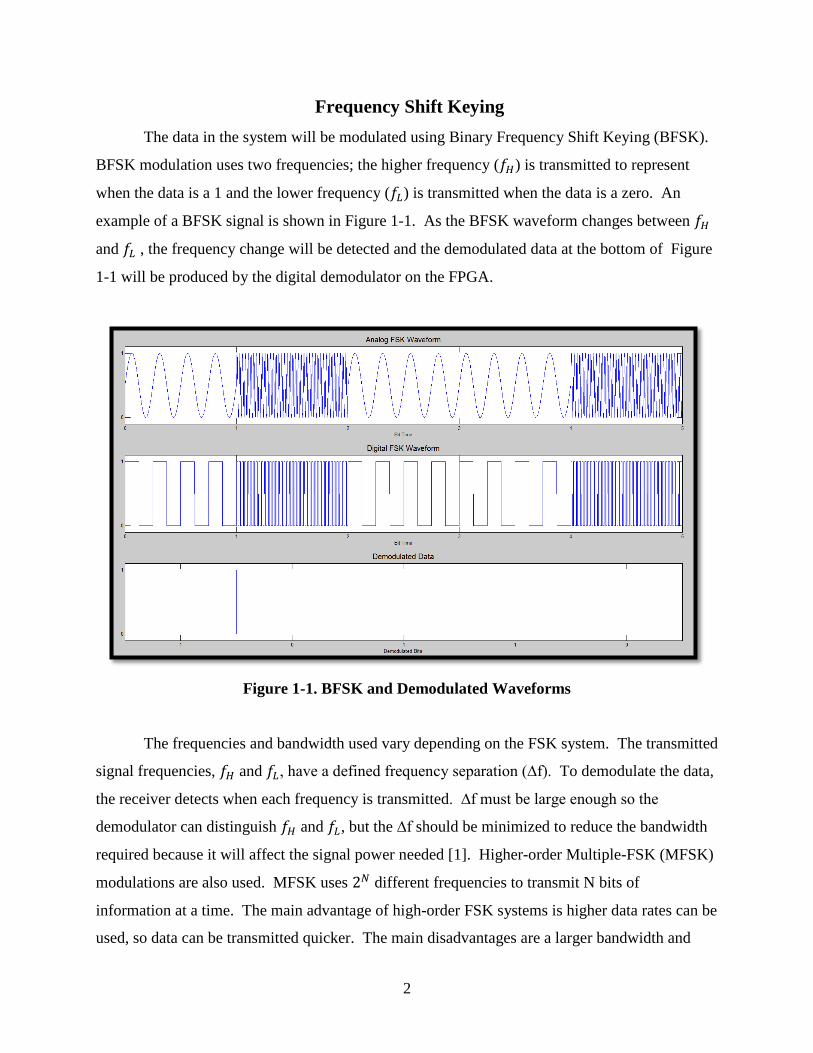
Frequency Shift Keying
The data in the system will be modulated using Binary Frequency Shift Keying (BFSK).
BFSK modulation uses two frequencies; the higher frequency (𝑓𝐻) is transmitted to represent
when the data is a 1 and the lower frequency (𝑓𝐿) is transmitted when the data is a zero. An
example of a BFSK signal is shown in Figure 1-1. As the BFSK waveform changes between 𝑓𝐻
and 𝑓𝐿 , the frequency change will be detected and the demodulated data at the bottom of Figure
1-1 will be produced by the digital demodulator on the FPGA.
Figure 1-1. BFSK and Demodulated Waveforms
The frequencies and bandwidth used vary depending on the FSK system. The transmitted
signal frequencies, 𝑓𝐻 and 𝑓𝐿, have a defined frequency separation (∆f). To demodulate the data,
the receiver detects when each frequency is transmitted. ∆f must be large enough so the
demodulator can distinguish 𝑓𝐻 and 𝑓𝐿, but the ∆f should be minimized to reduce the bandwidth
required because it will affect the signal power needed [1]. Higher-order Multiple-FSK (MFSK)
modulations are also used. MFSK uses 2𝑁 different frequencies to transmit N bits of
information at a time. The main advantage of high-order FSK systems is higher data rates can be
used, so data can be transmitted quicker. The main disadvantages are a larger bandwidth and
3
more power are required and the demodulation is more complex. The work in this paper will
focus only on BFSK demodulation.
Demodulation Methods
FSK modulated signals can be demodulated in several ways. Common techniques
include coherent and non-coherent detection methods that use filtering and comparators to
determine the frequency received. A phase-locked loop (PLL) could also be used. A PLL can
track the input frequency changes, but the PLL complexity may be excessive for a low power
application since BFSK demodulation only needs to distinguish between two frequencies. These
common methods, though proven and effective, require more power and increased design space
on the FPGA than some simpler demodulators, so other demodulation solutions were pursued.
The four methods investigated were a Counter, a One-Shot edge detector, a Phase Frequency
Detector (PFD), and a PFD with a pre-processor. Each method is introduced below and
discussed in more detail in chapter 3.
The Counter was used as a period detector. The frequency of each BFSK frequency, 𝑓𝐻
and 𝑓𝐿, will be significantly different similarly the period length, 𝑇𝐻 and 𝑇𝐿, of each BFSK input
will be significantly different. The Counter measures the period length by counting the number
of clock cycles during the period of the input. The counter value will rise and fall with the input
period length. A threshold value will be set between the expected values for a 𝑇𝐻 and 𝑇𝐿, and the
input will be demodulated to a 1 or 0 based on the counter value relative to the threshold.
The One-Shot demodulator detects the edges of the input signal. The signal is
demodulated by detecting when more or fewer edges are present over a time period. More edges
indicate a higher frequency which is used to determine when the input is 𝑓𝐻 or 𝑓𝐿. This
demodulator will output a pulse with each edge detected. The length of the generated pulse is
𝑇𝐻, so the pulse output for a 𝑓𝐻 input will be constantly high. When the input is 𝑓𝐿,the output
will be a pulse train where the duty cycle (D) can be found with equation 1.1. The output will be
filtered to find the average value of the signal. The output during 𝑓𝐻 will be at or near the
maximum value, and the output during 𝑓𝐿 will be near D. A threshold will be set between the
4
expected values. The actual value being above or below the threshold will determine if the input
is demodulated to a 1 or 0.
𝐷 = 𝑇𝐻/(𝑇𝐿 − 𝑇𝐻) (1.1)
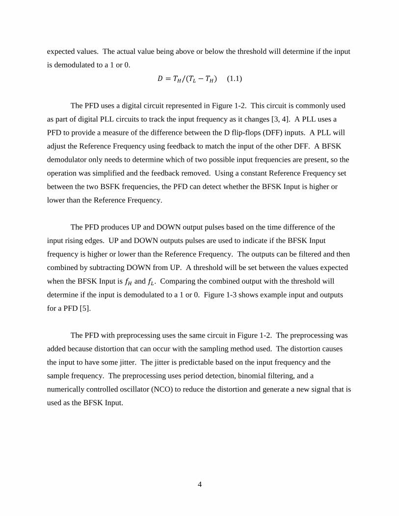
The PFD uses a digital circuit represented in Figure 1-2. This circuit is commonly used
as part of digital PLL circuits to track the input frequency as it changes [3, 4]. A PLL uses a
PFD to provide a measure of the difference between the D flip-flops (DFF) inputs. A PLL will
adjust the Reference Frequency using feedback to match the input of the other DFF. A BFSK
demodulator only needs to determine which of two possible input frequencies are present, so the
operation was simplified and the feedback removed. Using a constant Reference Frequency set
between the two BSFK frequencies, the PFD can detect whether the BFSK Input is higher or
lower than the Reference Frequency.
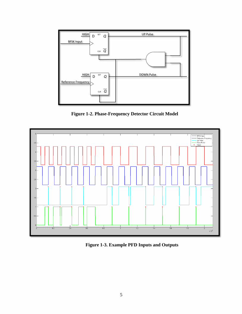
The PFD produces UP and DOWN output pulses based on the time difference of the
input rising edges. UP and DOWN outputs pulses are used to indicate if the BFSK Input
frequency is higher or lower than the Reference Frequency. The outputs can be filtered and then
combined by subtracting DOWN from UP. A threshold will be set between the values expected
when the BFSK Input is 𝑓𝐻 and 𝑓𝐿. Comparing the combined output with the threshold will
determine if the input is demodulated to a 1 or 0. Figure 1-3 shows example input and outputs
for a PFD [5].
The PFD with preprocessing uses the same circuit in Figure 1-2. The preprocessing was
added because distortion that can occur with the sampling method used. The distortion causes
the input to have some jitter. The jitter is predictable based on the input frequency and the
sample frequency. The preprocessing uses period detection, binomial filtering, and a
numerically controlled oscillator (NCO) to reduce the distortion and generate a new signal that is
used as the BFSK Input.
5
Figure 1-2. Phase-Frequency Detector Circuit Model
Figure 1-3. Example PFD Inputs and Outputs
Q
QSET
CLR
D
Q
QSET
CLR
D
UP Pulse
DOWN Pulse
HIGH
HIGH
BFSK Input
Reference Frequency
6
Chapter 2 - Sampling
When a signal is sampled correctly, the original frequency information can be recovered
from the set of samples. The forms of equation 2.1 show the Nyquist sampling theorem specifies
the sample frequency (𝑓𝑠) must be at least twice the bandwidth (BW) of the sampled signal to
preserve the information in the original signal (𝑓𝑖𝑛) similarly a sample must be taken at least at
the Nyquist sample interval, (𝑇𝑠).
𝑓𝑠 ≥ 2 ∗ 𝐵𝑊 (2.1a)
𝑇𝑠 ≤ 1
2𝐵𝑊 (2.1b)
To maintain the actual frequencies in 𝑓𝑖𝑛, it must be sampled at twice the maximum
frequency (𝑓𝑚) present in the signal.
𝑓𝑠 ≥ 2 ∗ 𝑓𝑚 (2.1c)
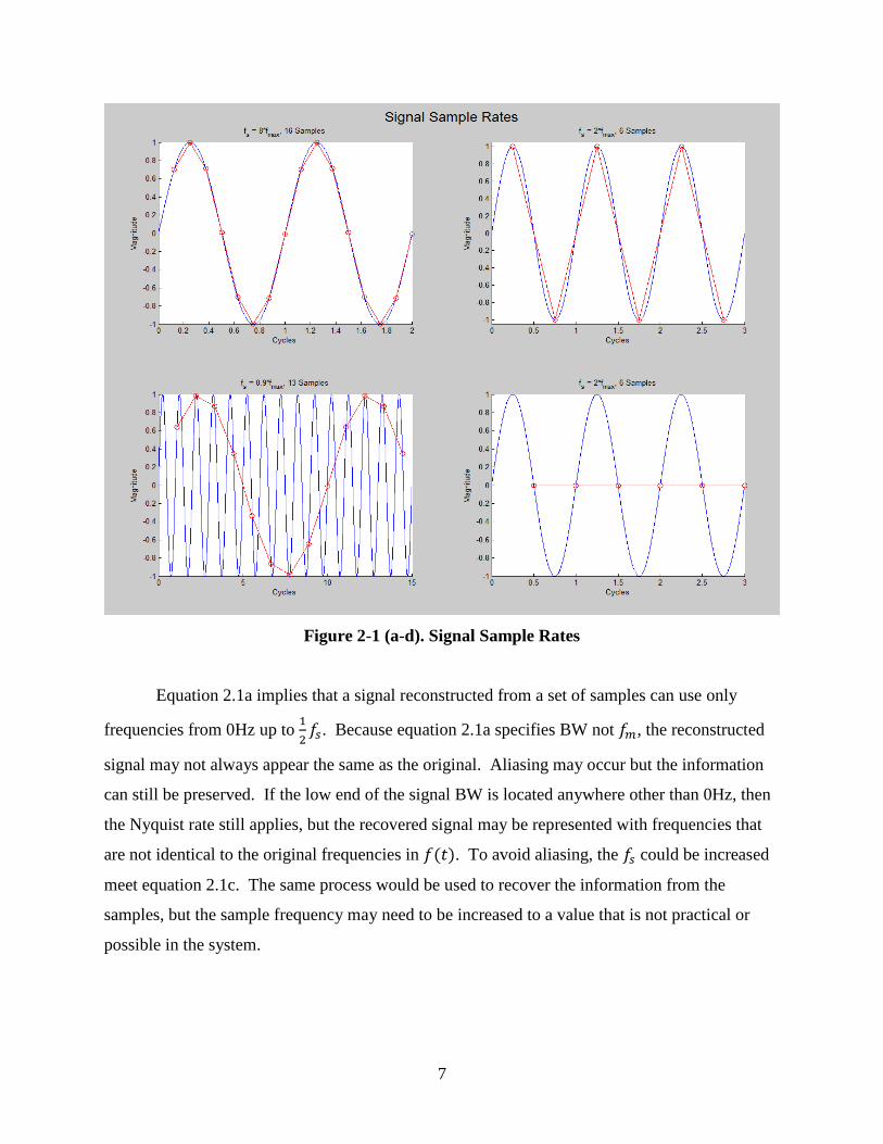
Figure 2-1 shows the result of a signal being sampled at several different rates and
examples of recovered waveforms based on those sample rates. The graphs show an input signal
(blue), sample points (red circles), and the recovered waveform from the samples (red). Figure
2-1a (top left) used 8 samples per cycle, 𝑓𝑠 = 8 ∗ 𝑓𝑚, and the samples preserved the signal
frequency and shape. Figure 2-1c (bottom left) used 0.9 samples per cycle, 𝑓𝑠 = 0.9 ∗ 𝑓𝑚. Too
few samples were taken to preserve the frequency, so the output is an aliased frequency. The
original frequency and alias are related through 𝑓𝑠, so if the alias and 𝑓𝑠 are known, the original
frequency may be determined.
Figures 2-1b (top right) and 2-1d (bottom right), both display what can happen if the
minimum rate of two samples per cycle is used, 𝑓𝑠 = 2 ∗ 𝑓𝑚. If the samples are taken when the
waveform is at its peak, the samples can recover the signal frequency and some of the shape.
The samples could just as likely be taken when the signal is at the zero crossings. The recovered
signal would be a dc value where no frequency or shape information could be successfully
recovered. These examples illustrate why the theoretical minimum number of samples per cycle
is two, but practically the number of samples taken per cycle should greater than two and
preferably several times higher when feasible.
7
Figure 2-1 (a-d). Signal Sample Rates
Equation 2.1a implies that a signal reconstructed from a set of samples can use only
frequencies from 0Hz up to 1
2𝑓𝑠. Because equation 2.1a specifies BW not 𝑓𝑚, the reconstructed
signal may not always appear the same as the original. Aliasing may occur but the information
can still be preserved. If the low end of the signal BW is located anywhere other than 0Hz, then
the Nyquist rate still applies, but the recovered signal may be represented with frequencies that
are not identical to the original frequencies in 𝑓(𝑡). To avoid aliasing, the 𝑓𝑠 could be increased
meet equation 2.1c. The same process would be used to recover the information from the
samples, but the sample frequency may need to be increased to a value that is not practical or
possible in the system.
8
Aliasing can be used intentionally while still preserving the frequency relationships in
𝑓(𝑡). When 𝐵𝑊 ≤ 𝑓𝑚, the signal information can be preserved despite the original frequencies
being lost. When the bandwidth does not start at 0Hz, equations 2.1a and 2.1c are no longer
equal because 𝑓𝑚 is greater than the BW. As 𝑓𝑚 increases, equation 2.1c may not be practical,
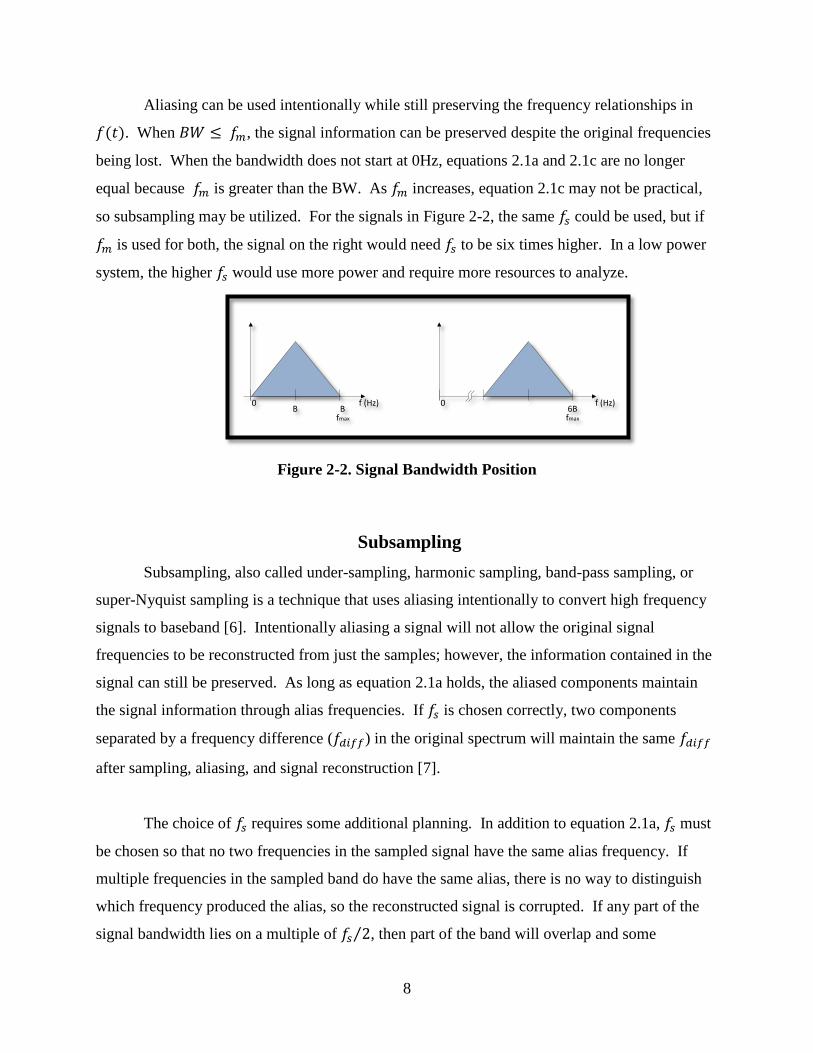
so subsampling may be utilized. For the signals in Figure 2-2, the same 𝑓𝑠 could be used, but if
𝑓𝑚 is used for both, the signal on the right would need 𝑓𝑠 to be six times higher. In a low power
system, the higher 𝑓𝑠 would use more power and require more resources to analyze.
Figure 2-2. Signal Bandwidth Position
Subsampling
Subsampling, also called under-sampling, harmonic sampling, band-pass sampling, or
super-Nyquist sampling is a technique that uses aliasing intentionally to convert high frequency
signals to baseband [6]. Intentionally aliasing a signal will not allow the original signal
frequencies to be reconstructed from just the samples; however, the information contained in the
signal can still be preserved. As long as equation 2.1a holds, the aliased components maintain
the signal information through alias frequencies. If 𝑓𝑠 is chosen correctly, two components
separated by a frequency difference (𝑓𝑑𝑖𝑓𝑓) in the original spectrum will maintain the same 𝑓𝑑𝑖𝑓𝑓
after sampling, aliasing, and signal reconstruction [7].
The choice of 𝑓𝑠 requires some additional planning. In addition to equation 2.1a, 𝑓𝑠 must
be chosen so that no two frequencies in the sampled signal have the same alias frequency. If
multiple frequencies in the sampled band do have the same alias, there is no way to distinguish
which frequency produced the alias, so the reconstructed signal is corrupted. If any part of the
signal bandwidth lies on a multiple of 𝑓𝑠 2⁄ , then part of the band will overlap and some
fs/2 fs 3fs/2
Fs/2
2fsf (Hz)
fs/2 fs 3fs/2 2fsf (Hz)
fs/2
fs
3fs/2
2fs
Original Spectrum
Recovered Spectrum with No Filter
Aliasing Diagram
fs/2 fs 3fs/2 2fsf (Hz)
Recovered Spectrum with Filter
Anti-Aliasing Filter
(c)
(b)
(a)(d)
f1 f2 f3
fa fb fc
f1 f2
f3
f1 f2
f3
f1 f2f3
f3
-B0
Bf (Hz)
fmax
6B0 f (Hz)
fmax
B Bf (Hz)
fmax
0
9
frequencies will have the same alias [8]. A simple way to find whether any frequencies will
share an alias is to divide the maximum and minimum frequencies in the signal by 𝑓𝑠 2⁄ , as
shown in equation 2.2. If the integer part of the quotients are equal, then none of the signal
bandwidth lies on a multiple of 𝑓𝑠 2⁄ .
𝑓𝑙𝑜𝑜𝑟 (𝑓𝑚𝑎𝑥
𝑓𝑠 2⁄) = 𝑓𝑙𝑜𝑜𝑟 (
𝑓𝑚𝑖𝑛
𝑓𝑠 2⁄) (2.2)
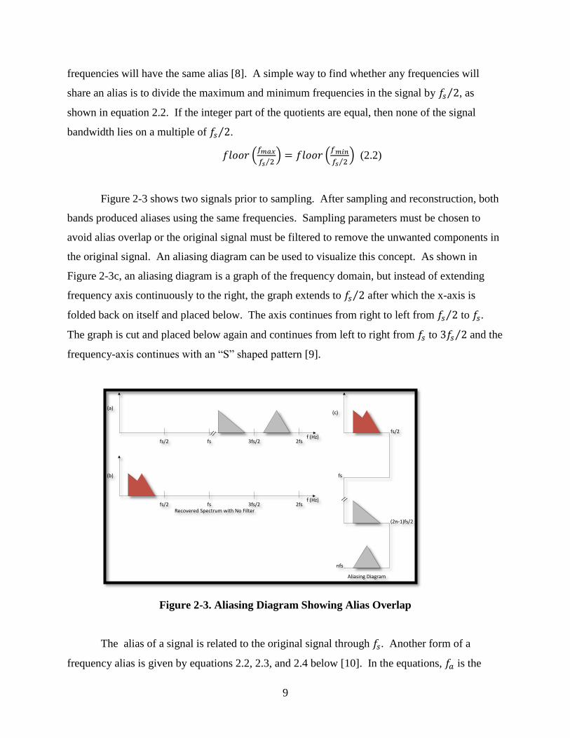
Figure 2-3 shows two signals prior to sampling. After sampling and reconstruction, both
bands produced aliases using the same frequencies. Sampling parameters must be chosen to
avoid alias overlap or the original signal must be filtered to remove the unwanted components in
the original signal. An aliasing diagram can be used to visualize this concept. As shown in
Figure 2-3c, an aliasing diagram is a graph of the frequency domain, but instead of extending
frequency axis continuously to the right, the graph extends to 𝑓𝑠 2⁄ after which the x-axis is
folded back on itself and placed below. The axis continues from right to left from 𝑓𝑠 2⁄ to 𝑓𝑠.
The graph is cut and placed below again and continues from left to right from 𝑓𝑠 to 3𝑓𝑠 2⁄ and the
frequency-axis continues with an “S” shaped pattern [9].
Figure 2-3. Aliasing Diagram Showing Alias Overlap
The alias of a signal is related to the original signal through 𝑓𝑠. Another form of a
frequency alias is given by equations 2.2, 2.3, and 2.4 below [10]. In the equations, 𝑓𝑎 is the
fs/2 fs 3fs/2 2fsf (Hz)
fs/2 fs 3fs/2 2fsf (Hz)
fs/2
fs
(2n-1)fs/2
nfs
Recovered Spectrum with No Filter
Aliasing Diagram
(b)
(a)(c)
//
//
10
aliased frequency, 𝑓𝑖𝑛 is the input signal frequency being sampled, 𝑓𝑠 is the sampling frequency,
and W is an integer which is selected so that 𝑓𝑎 is minimized. W can be found by taking the ratio
of 𝑓𝑖𝑛 𝑓𝑠⁄ and rounding to the nearest integer. R represents the fractional remainder rounded off
to make W an integer.
𝑓𝑎(𝑊) = |𝑓𝑖𝑛 − 𝑊𝑓𝑠| (2.2)
𝑊 + 𝑅 = 𝑓𝑖𝑛 𝑓𝑠⁄ (2.3)
𝑓𝑎 = 𝑅 ∗ 𝑓𝑠 (𝑅 ≤ 0.5) (2.4𝑎)
𝑓𝑎 = (1 − 𝑅) ∗ 𝑓𝑠 (𝑅 > 0.5) (2.4𝑏)
For example, if 𝑓𝑖𝑛 = 10.7𝑀𝐻𝑧 and 𝑓𝑠 = 500𝑘𝐻𝑧, 𝑓𝑖𝑛 𝑓𝑠 = 21.4⁄ , then 𝑊 = 21 and
𝑅 = 0.4 = 2 5⁄ . The alias frequency can be found using equation 2.2. 𝑓𝑎 = |10.7𝑀𝐻𝑧 − 21 ∗
500𝑘𝐻𝑧| = 200𝑘𝐻𝑧.
If present, undesired signals outside of the desired spectrum may alias to the same
frequency as part of the desired spectrum. Any signal above 𝑓𝑠 2⁄ will be aliased to some
frequency in the range of the reconstructed signal spectrum, from 0Hz to 𝑓𝑠 2⁄ . If undesired
signals are not accounted for, the reconstructed signal could be corrupted by the alias of an
undesired signal. Theoretically an infinite number of frequencies could alias to the same
frequency. Though an infinite number of those frequencies will likely not appear in the system,
some may be present. The aliased frequency will be a copy of the original frequency that is
shifted down by a multiple of 𝑓𝑠. The multiple is represented by W in equation 2.3. There is an
𝑓𝑖𝑛 for each value of W that will result in the same alias frequency. One frequency on each level
of the aliasing diagram in Figure 2-3 would alias to one of the reconstructed alias frequencies.
The 𝑓𝑖𝑛 values that have the same alias are spaced by 𝑓𝑠 in the original signal. This is one reason
why subsampling must be done carefully. Using equation 2.2, the values of 𝑓𝑖𝑛that alias to the
same frequency can be found. If 𝑓𝑎 = 200𝑘𝐻𝑧 and 𝑓𝑠 = 500𝑘𝐻𝑧, different values of 𝑓𝑖𝑛with the
same alias can be found by plugging in values for W. Choosing example W values of 1, 5, 10,
15, and 25, 𝑓𝑖𝑛 components of 700kHz, 2.7MHz, 5.2MHz, 7.7MHz, and 12.7MHz respectively,
all will alias to 200kHz when 𝑓𝑠 is 500kHz.
11
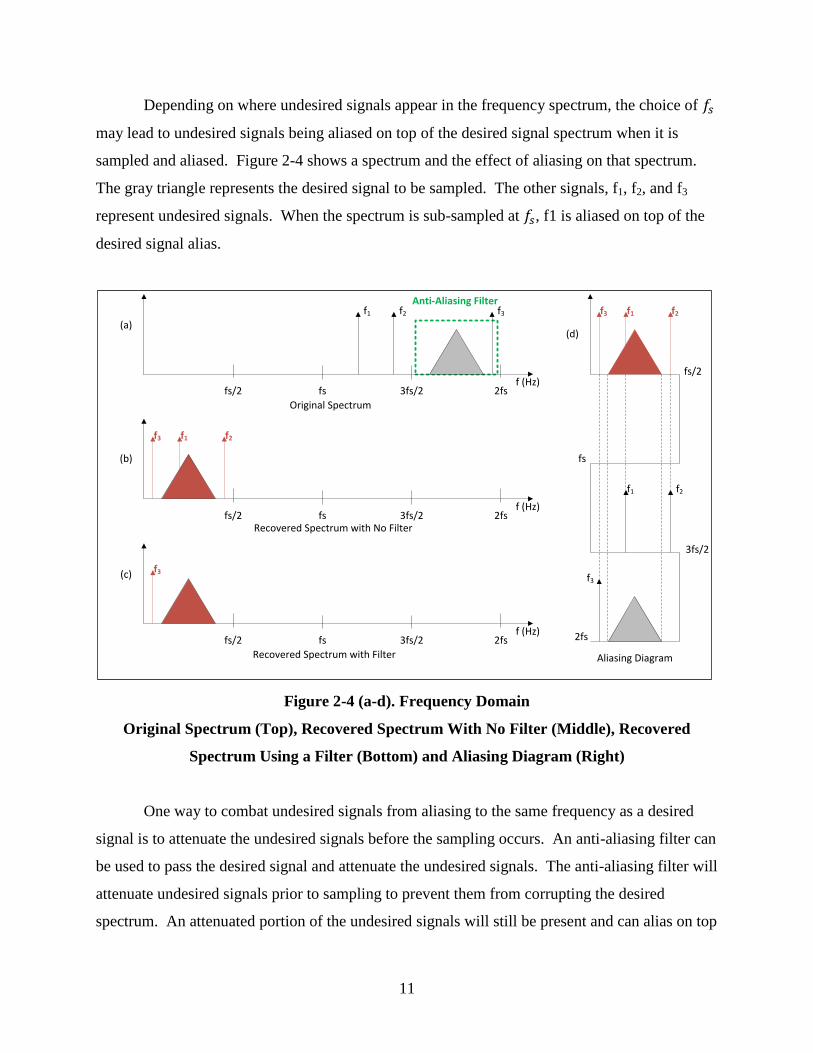
Depending on where undesired signals appear in the frequency spectrum, the choice of 𝑓𝑠
may lead to undesired signals being aliased on top of the desired signal spectrum when it is
sampled and aliased. Figure 2-4 shows a spectrum and the effect of aliasing on that spectrum.
The gray triangle represents the desired signal to be sampled. The other signals, f1, f2, and f3
represent undesired signals. When the spectrum is sub-sampled at 𝑓𝑠, f1 is aliased on top of the
desired signal alias.
Figure 2-4 (a-d). Frequency Domain
Original Spectrum (Top), Recovered Spectrum With No Filter (Middle), Recovered
Spectrum Using a Filter (Bottom) and Aliasing Diagram (Right)
One way to combat undesired signals from aliasing to the same frequency as a desired
signal is to attenuate the undesired signals before the sampling occurs. An anti-aliasing filter can
be used to pass the desired signal and attenuate the undesired signals. The anti-aliasing filter will
attenuate undesired signals prior to sampling to prevent them from corrupting the desired
spectrum. An attenuated portion of the undesired signals will still be present and can alias on top
fs/2 fs 3fs/2
Fs/2
2fsf (Hz)
fs/2 fs 3fs/2 2fsf (Hz)
fs/2
fs
3fs/2
2fs
Original Spectrum
Recovered Spectrum with No Filter
Aliasing Diagram
fs/2 fs 3fs/2 2fsf (Hz)
Recovered Spectrum with Filter
Anti-Aliasing Filter
(c)
(b)
(a)(d)
f1 f2 f3
fa fb fc
f1 f2
f3
f1 f2
f3
f1 f2f3
f3
12
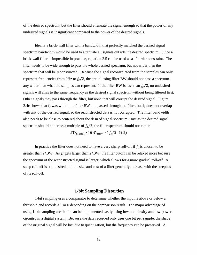
of the desired spectrum, but the filter should attenuate the signal enough so that the power of any
undesired signals is insignificant compared to the power of the desired signals.
Ideally a brick-wall filter with a bandwidth that perfectly matched the desired signal
spectrum bandwidth would be used to attenuate all signals outside the desired spectrum. Since a
brick-wall filter is impossible in practice, equation 2.5 can be used as a 1st order constraint. The
filter needs to be wide enough to pass the whole desired spectrum, but not wider than the
spectrum that will be reconstructed. Because the signal reconstructed from the samples can only
represent frequencies from 0Hz to 𝑓𝑠 2⁄ , the anti-aliasing filter BW should not pass a spectrum
any wider than what the samples can represent. If the filter BW is less than 𝑓𝑠 2⁄ , no undesired
signals will alias to the same frequency as the desired signal spectrum without being filtered first.
Other signals may pass through the filter, but none that will corrupt the desired signal. Figure
2.4c shows that f3 was within the filter BW and passed through the filter, but f3 does not overlap
with any of the desired signal, so the reconstructed data is not corrupted. The filter bandwidth
also needs to be close to centered about the desired signal spectrum. Just as the desired signal
spectrum should not cross a multiple of 𝑓𝑠 2⁄ , the filter spectrum should not either.
𝐵𝑊𝑠𝑖𝑔𝑛𝑎𝑙 ≤ 𝐵𝑊𝑓𝑖𝑙𝑡𝑒𝑟 ≤ 𝑓𝑠 2⁄ (2.5)
In practice the filter does not need to have a very sharp roll-off if 𝑓𝑠 is chosen to be
greater than 2*BW. As 𝑓𝑠 gets larger than 2*BW, the filter cutoff can be relaxed more because
the spectrum of the reconstructed signal is larger, which allows for a more gradual roll-off. A
steep roll-off is still desired, but the size and cost of a filter generally increase with the steepness
of its roll-off.
1-bit Sampling Distortion
1-bit sampling uses a comparator to determine whether the input is above or below a
threshold and records a 1 or 0 depending on the comparison result. The major advantage of
using 1-bit sampling are that it can be implemented easily using low complexity and low-power
circuitry in a digital system. Because the data recorded only uses one bit per sample, the shape
of the original signal will be lost due to quantization, but the frequency can be preserved. A
13
signal transmitting data using BFSK can work well with 1-bit sampling since the data is
transmitted using changes in frequency. The signal to be sampled will be centered at 10.7MHz
and provided by a radio frequency integrated circuit (RFIC) designed at Kansas State University
[11].
The ratio of input frequency to the sample frequency indicates how often a sample is
taken. Using the values from the previous aliasing example, 𝑓𝑖𝑛 𝑓𝑠 =10.7𝑀𝐻𝑧
500𝑘𝐻𝑧= 21.4⁄ , one
sample will be taken every 21.4 cycles of the input. Using equation 2.3 and 2.4, W = 21, R =
0.4, and 𝑓𝑎 = 200𝑘𝐻𝑧. The R value can be used to find the alias frequency. The aliasing
diagram in Figure 2-4 shows visually where a frequency will alias. The W value in the ratio
represents how many levels down on the diagram that 𝑓𝑖𝑛 is, and R represents the position of the
frequency on the level. As R gets closer to 0, the alias frequency decreases, and as R gets closer
to its maximum value of 0.5, the alias frequency increases. This happens because R represents
the phase shift between each sample taken. With this example there are 21.4 cycles of the input
signal between each sample. If the first sample is taken at the rising edge of a signal or 0° phase,
the next would be 21.4 cycles later at 0.4*360° = 144°. The subsequent samples would also shift
in phase by 40% of a cycles or 144°. Using a sine wave as an example, the sample will be a 1 if
taken when the phase is from 0° - 180° and a 0 if taken from 180° - 360°. Regardless of the
number of whole cycles skipped between samples, the phase shift, represented by R, is the same.
A larger change in phase between samples means the value of the sampled value will change
more often, so the alias frequency will be higher.
A problem that arises when using 1-bit sampling is the waveform reconstructed from the
samples usually will not have a 50% duty cycle or a consistent period. The single bit in the
samples at the given sample rate does not always provide enough resolution for the samples to
perfectly reconstruct every frequency from 0Hz to 𝑓𝑠 2⁄ . The sample is either a 1 or 0 and only
indicates whether the cycle was on the top half or bottom half of the cycle when that sample was
taken. The input may have been right at a peak, a zero-crossing, or anywhere in between. When
undersampling and using one-bit sampling like this, the samples can rarely reconstruct a
waveform to perfectly match the expected alias frequency. The frequency can still be
reproduced, but the waveform will be reconstructed using a combination of the closest frequency
14
above and closest frequency below the expected alias. The reconstructed signal will alternate
between the two frequencies with a repeating pattern. The average frequency over the full
pattern will be the expected alias frequency. The reconstructed wave will have a distorted
appearance because of the frequency changing back and forth. The distortion is related to the
ratio, R, from equation 2.4a.
R is similar to the inverse of the sample rate. If R, the ratio of the input frequency to the
sampling frequency, has a remainder of 0.42, then a sample will be taken every 0.42 cycles, or
there will be 1/R = 2.38 samples per cycle. The number of samples per cycle is not an integer, so
there may be either two or three samples taken during a single cycle in this case depending on
the phase of the first sample. If an inconsistent number of samples are used to reconstruct each
cycle in the waveform, the reconstructed cycles will necessarily have inconsistent period lengths
and therefore an inconsistent frequency. Some cycles will have a longer or shorter period by one
sample, but the period lengths in the waveform will follow a repeating pattern. Since the
frequency cannot be represented in a single cycle, the reconstructed waveform produces a pattern
using long and short periods, or a higher and lower frequency that will average out to the
expected frequency over a complete pattern. If R = 0.42, there are 2.38 samples per cycle, so
38% of the input cycles will be sampled three times and the remaining 62% of the cycles will
only be sampled two times. The rational form of R, seen in equation 2.6, can be used to find the
number of cycles (N) and the number of samples (M) in the whole pattern. N/M = 42/100 =
21/50, so there will be 21 cycles made of 50 samples in the repeating pattern that is formed. Not
all frequencies will require that many samples or cycles for a pattern. Some patterns require only
two samples, but some patterns require hundreds of samples to complete a pattern.
𝑅 = 𝑁 𝑀⁄ (2.6)
𝑅 − 1 = (1 − 𝑁) 𝑀⁄ (2.7)
The alias frequency and both the frequencies that will be averaged to get the alias
frequency can be determined using the same ratio. From equation 2.4, the alias will be R times
𝑓𝑠/2. When rounded up or down, the inverse of R indicates the number of samples that will be
used to reconstruct the long or short periods of the waveform respectively. The sample
frequency divided by those rounded values of R give the frequencies produced. For example, if
15
the input was 54.2kHz with a 10kHz sample rate, R = 0.42 = N/M = 21/50. The alias frequency
would be 0.42*10kHz = 4.2kHz. There would be two or three samples per period, so fL = fs/3 =
3.33kHz and fH = fs/2 = 5kHz.
The following example with Figure 2-5a-d illustrates what happens when 1-bit distortion
occurs. When the number of samples per cycle is inconsistent, the waveform periods get
lengthened and shortened as more and fewer samples are used in a given cycle. An additional
sample in a cycle causes the waveform to stay high or low for another sample time interval. The
samples will be taken in time intervals that are multiples of R. Using R = 0.4 = N/M = 2/5, the
pattern will be two cycles long and have five samples. Because 1-bit sampling is used, samples
with a decimal value of 0.5 or above are ones and samples with a decimal value below 0.5 are
zeros. Assume that the sampling starts with the beginning of the first cycle at time 0.0s and 0°.
The sample times in terms of cycles will be R = 0.4, 0.8, 1.2, 1.6, 2.0, … The integer portion of
the terms are ignored, and the samples are converted to a 1 or 0 based on the range they are in.
The sampled result will repeat the five-sample pattern: 0-1-0-1-0. The sampled waveform
pattern will average out to be the correct frequency using equation 2.4. The average period when
taken over the full pattern is equal the expected period based on equation 2.4a.
Figure 2-5 below shows an input signal sampled at two different rates and the
reconstructed waveforms. Fig 2-5a and 2-5c show the original signal with the sample points
marked for 𝑓𝑠 = 0.4𝑀𝐻𝑧 and 𝑓𝑠 = 0.5𝑀𝐻𝑧 on the input signal. Figure 2-5b and 2-5d show the
respective reconstructed, aliased waveforms. The different sample rates show how the aliased
output can be a consistent frequency or a combination of two frequencies.
The trivial solution for the problem of signal aliases having inconsistent periods would be
to make sure that any frequencies used have a remainder where N = 1 or 1-N = 1 so that no extra
processing was required to extract the actual alias frequencies. If possible that would be great,
but non-idealities in a real systems cause frequencies to not always be perfectly generated,
transmitted, or received, so the received signal may drift up or down in frequency from what is
expected even if the system is setup carefully. The most straight forward way to get the true
alias frequency or at least get close to it is to average the periods over a number of cycles. The
16
best method would be to match the number of cycles in an alias pattern with the number of
cycles averaged, but that is not always practical especially as full patterns can be lengthy, and
non-ideal signals have extra error introduced through jitter, frequency drift, and noise.
Figure 2-5 (a-d). 1-bit Sampling Distortion Examples
Averaging
The most apparent solution to reduce the problems caused by the 1-bit sampling
distortion is to take the average over several periods of the sampled waveform to get more
accurate values for the period and frequency. The problem with averaging is that the length of
the patterns representing different frequencies varies. Using, 𝑅 = 𝑁 𝑀⁄ , M samples are needed
to complete the N cycles in a pattern. Another way to look at it is 𝑅−1 cycles are needed
complete the pattern. If 𝑅−1 is not an integer, then the first multiple of 𝑅−1 that is an integer
indicates how many cycles need to be averaged to find the period. A signal can require
anywhere from one to hundreds of cycles or more to complete waveform pattern. No matter how
many cycles are averaged, the result will not be perfect for most frequencies, but averaging can
still be a significant help and give a good approximation to the actual alias frequency.
17
A whole pattern may not be needed to get a good estimate of a signal period. Though a
fraction like 𝑁/𝑀 = 5001 10000⁄ technically requires 5001 cycles to be averaged to find the
exact average, the fraction is close to 1 2⁄ which needs no averaging. For most patterns, a
practical middle ground can be found. Most long patterns look very similar to a shorter pattern.
A shorter averaging window can be used which will reduce the overall effect of the distortion
and give a close estimate to the actual value. Figure 2-6 below shows the pattern for a frequency
with R=17/100. The figure used samples per period vs total samples to show the inconsistent
period length. The expected average of the samples (red) and the 3-period moving average
(green) are shown.
Figure 2-6. Period Averaging Example, R = 17/100
The error between the reconstructed signal and the expected average can be measured for
each period and accumulated using the mean squared error (MSE). The effect of averaging to
reduce the error will be tested for different R values. The error values will be checked for R
values from 1/100 to 50/100 in steps of 1/100. R values above 0.5 produce duplicate, mirrored
values and are not shown. Figure 2-7 shows the accumulated MSE over 1000 samples with no
averaging. Figure 2-8 shows the accumulated MSE over 1000 samples after a length of 8
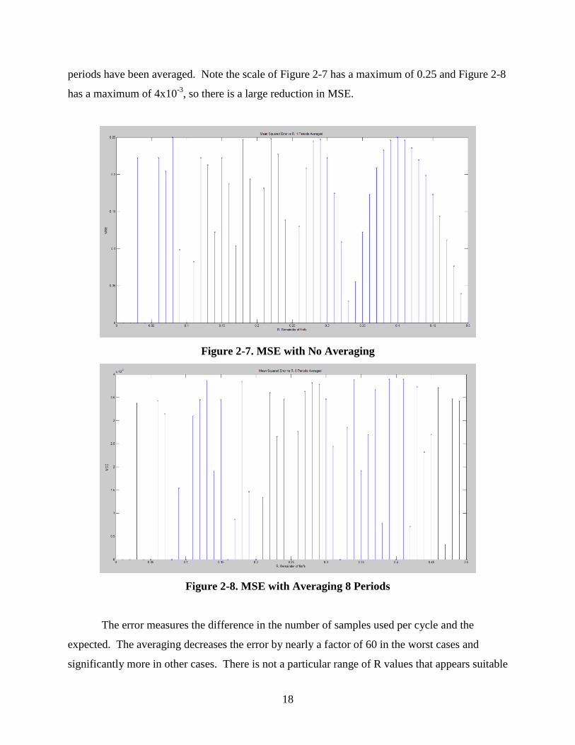
18
periods have been averaged. Note the scale of Figure 2-7 has a maximum of 0.25 and Figure 2-8
has a maximum of 4x10⁻³
, so there is a large reduction in MSE.
Figure 2-7. MSE with No Averaging
Figure 2-8. MSE with Averaging 8 Periods
The error measures the difference in the number of samples used per cycle and the
expected. The averaging decreases the error by nearly a factor of 60 in the worst cases and
significantly more in other cases. There is not a particular range of R values that appears suitable
19
to focus on aliasing signals to that area. Some particular values are better than others, but the
averaging helps no matter where in the spectrum the signal is aliased. Averaging over a larger
number of cycles would reduce the error even more. The easiest averaging choice for digital
systems would be a power of two because the divide operation can be implemented in a
hardware design language (HDL) easily using a shift operator if the divide is a power of two.
Chapter 3 - Demodulator Design
The signal demodulation will occur after the 1-bit sampling has occurred. The BFSK
frequencies will be in the kHz range after the sampling and waveform reconstruction. This will
allow the demodulators to run at a lower clock frequency contributing to power conservation in
the digital design. To reduce the effects of 1-bit sampling distortion, accumulating over multiple
periods, using a moving average filter, or binomial average filter were explored as possible
solutions for each demodulator [12]. Each of the demodulators were tested using parameters
taken from [13]. The IF 𝑓ℎ, 𝑓𝑙 BFSK frequencies were 10.71MHz and 10.69MHz with a 1kbps
data rate. After 1-bit sampling at 75kHz, the baseband 𝑓ℎ, 𝑓𝑙 BFSK frequencies used at the input
to the demodulators were 35kHz and 15kHz.
Counter
The counter demodulator uses a counter to measure the time between positive edges of
the input signal, 𝑓𝑖𝑛. If the period of the BFSK frequencies can be counted, measured, and
distinguished from each other, then the data in 𝑓𝑖𝑛 can be demodulated. The number of clock
cycles between the positive edges of 𝑓𝑖𝑛 measure the period, 𝑇𝑖𝑛. The clock used for the count is
the input clock driving the FPGA demodulator module. The counter output signal can be
represented using equation 3.1. As the input changes between 𝑓𝐻 and 𝑓𝐿, the value of Ncount
produces a pseudo-square wave that mimics the values modulated data. The value of Ncount is
inversely proportional to the input frequency. The output from the counter will need to be an
actual digital signal, so the output will be created by comparing the Ncount waveform to a
threshold value. When Ncount is above or below the threshold, the output will be demodulated to
a 1 or 0 respectively.
𝑁𝑐𝑜𝑢𝑛𝑡 = 𝑓𝑐𝑙𝑘 𝑓𝑖𝑛 (3.1)⁄
20
The counter demodulator would benefit from the FPGA clock running at a high
frequency. More clock cycles per 𝑓𝑖𝑛 cycle allows higher count values and a larger difference
between Ncount for 𝑓𝐿 and 𝑓𝐻. The value Ncount can also be increased by accruing the count over
multiple cycles of 𝑓𝑖𝑛. Ncount is accumulated over several periods to reduce the effects of the 1-
bit distortion. The accumulation required additional registers in the HDL design, and the output
would be delayed, but the output would have more consistent and clearly defined data
transitions. Using a count accumulated over multiple cycles also helps increase the difference
between the values for each BFSK frequency.
The HDL counter design consists of two blocks, the edge detector and the counter with
accumulator. The counter increments on every system clock edge. The edge detector detects the
edges of the input signal and prompts the counter to output the current value and start a new
count. Ncount is the sum of the most recent four count values.
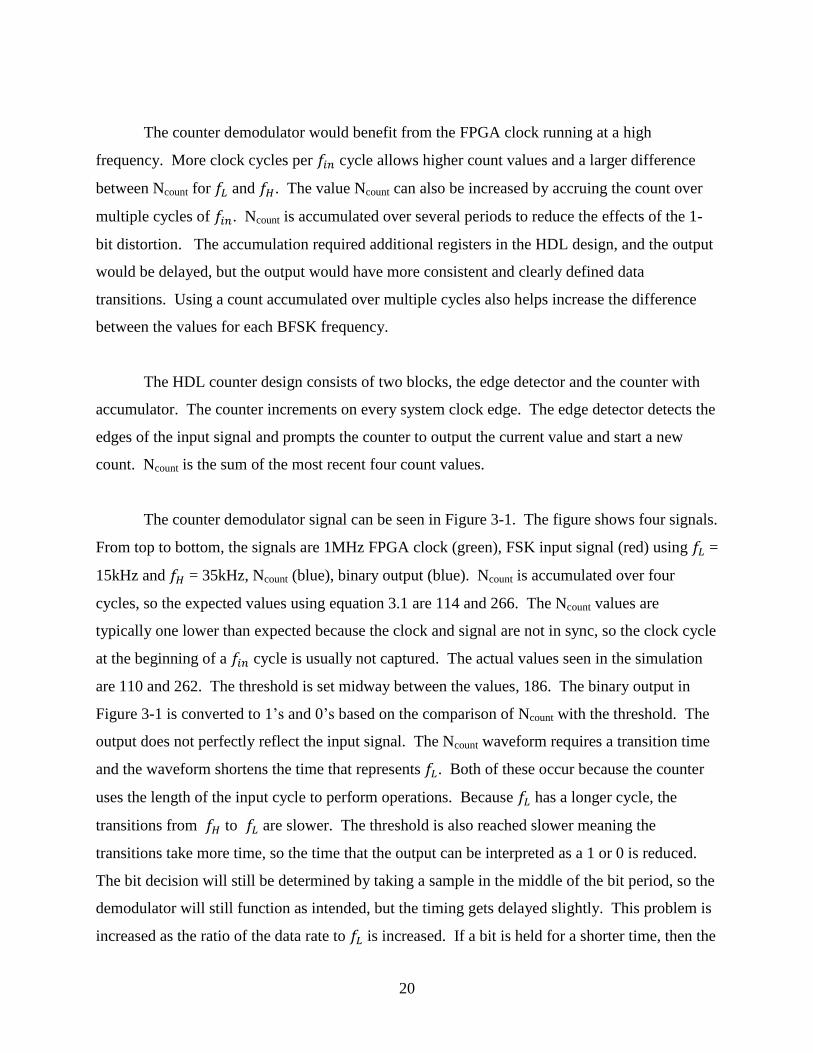
The counter demodulator signal can be seen in Figure 3-1. The figure shows four signals.
From top to bottom, the signals are 1MHz FPGA clock (green), FSK input signal (red) using 𝑓𝐿 =
15kHz and 𝑓𝐻 = 35kHz, Ncount (blue), binary output (blue). Ncount is accumulated over four
cycles, so the expected values using equation 3.1 are 114 and 266. The Ncount values are
typically one lower than expected because the clock and signal are not in sync, so the clock cycle
at the beginning of a 𝑓𝑖𝑛 cycle is usually not captured. The actual values seen in the simulation
are 110 and 262. The threshold is set midway between the values, 186. The binary output in
Figure 3-1 is converted to 1’s and 0’s based on the comparison of Ncount with the threshold. The
output does not perfectly reflect the input signal. The Ncount waveform requires a transition time
and the waveform shortens the time that represents 𝑓𝐿. Both of these occur because the counter
uses the length of the input cycle to perform operations. Because 𝑓𝐿 has a longer cycle, the
transitions from 𝑓𝐻 to 𝑓𝐿 are slower. The threshold is also reached slower meaning the
transitions take more time, so the time that the output can be interpreted as a 1 or 0 is reduced.
The bit decision will still be determined by taking a sample in the middle of the bit period, so the
demodulator will still function as intended, but the timing gets delayed slightly. This problem is
increased as the ratio of the data rate to 𝑓𝐿 is increased. If a bit is held for a shorter time, then the
21
transition time becomes more significant. The simulation in Figure 3-1 does not include 1-bit
distortion. The inputs are ideal 15kHz and 35kHz signals.
Figure 3-1. Counter Demodulator Simulation
One-Shot
The One-Shot demodulator detects the signal edges of an FSK input signal [13]. The
number of edges over a period of time is proportional to the frequency of the signal. Over a set
period of time, the number of edges can be used to detect whether the FSK input is 𝑓𝐻 or 𝑓𝐿 .
The number of edges over a period of time can be counted and the result viewed as a pseudo-
analog value that is proportional to the input data.
When an edge is detected on the input, the demodulator produces a pulse. The length of
the pulse is designed to be the same length as a period of 𝑓𝐻. With the input at 𝑓𝐻, the output
pulses will run together producing a constant value until the input changes to 𝑓𝐿. When the input
is 𝑓𝐿, the edges will occur less often. The produced pulses remain the same length and occur at
every positive edge as before. Since there are fewer edges, and those edges are more spread out,
the average value of the output when the input is 𝑓𝐿 will be lower.
The average value of the output pulses over a time interval can be used to demodulate the
input. The average values taken from the output pulses give a pseudo-analog waveform that
represents the data modulated in the input. The waveform can be converted back to a binary
signal by finding an appropriate threshold value and comparing it to against the One-Shot output.
The result indicates when the signal should be demodulated to a 1 or 0.
The HDL design uses three blocks. One module detects the edges of the input BFSK
signal. Another produces a pulse for each edge detected. The last module averages the pulsed
signal to make the pseudo-analog waveform and then the bit decision based on the threshold to
22
demodulate the waveform to a 1 or 0. The output can then be put into a bit-sync module. The
clock running at the bit rate can be synced with the data. The middle of the bit period can be
found, and the data can be sampled to produce the final demodulated output.
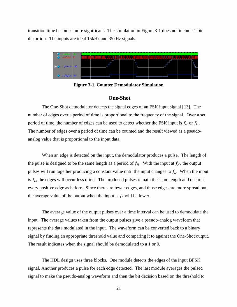
Simulated signals from the One-shot demodulator are shown in Figure 3-2. From top to
bottom the signals in the figure are the system clock (green), FSK input (blue), edge detector
output (blue), output pulse (red), averaged pulse (light green), binary output (yellow). As a scale
reference, the yellow vertical bar on the ride edge of the figure intersects the averaged pulse
waveform near the median value, 950. The simulation in Figure 3-2 does not include 1-bit
distortion. The inputs are ideal 15kHz and 35kHz signals.
Figure 3-2. One-Shot Simulation
Phase-Frequency Detector
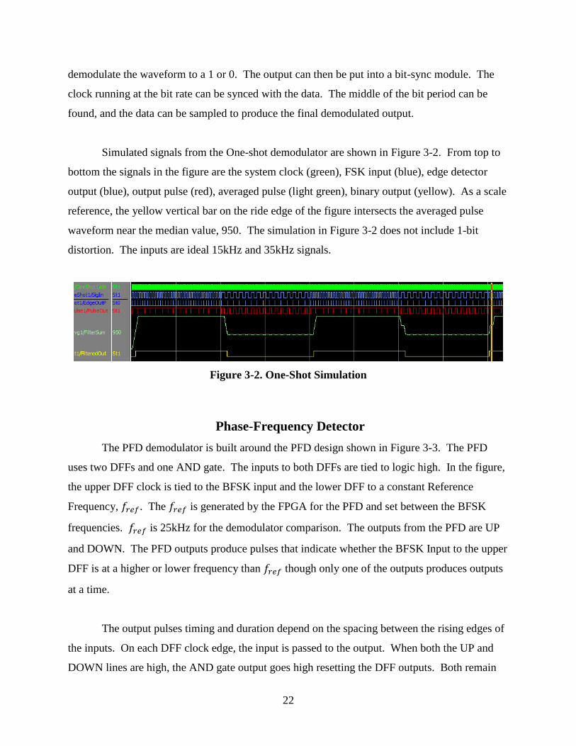
The PFD demodulator is built around the PFD design shown in Figure 3-3. The PFD
uses two DFFs and one AND gate. The inputs to both DFFs are tied to logic high. In the figure,
the upper DFF clock is tied to the BFSK input and the lower DFF to a constant Reference
Frequency, 𝑓𝑟𝑒𝑓. The 𝑓𝑟𝑒𝑓 is generated by the FPGA for the PFD and set between the BFSK
frequencies. 𝑓𝑟𝑒𝑓 is 25kHz for the demodulator comparison. The outputs from the PFD are UP
and DOWN. The PFD outputs produce pulses that indicate whether the BFSK Input to the upper
DFF is at a higher or lower frequency than 𝑓𝑟𝑒𝑓 though only one of the outputs produces outputs
at a time.
The output pulses timing and duration depend on the spacing between the rising edges of
the inputs. On each DFF clock edge, the input is passed to the output. When both the UP and
DOWN lines are high, the AND gate output goes high resetting the DFF outputs. Both remain
23
outputs remain low until an input has a rising edge. Because the outputs depend on the timing of
the inputs, the UP and DOWN pulses have an inconsistent pattern, but the output pulse trends
show the frequency relationship between 𝑓𝑟𝑒𝑓 and the BFSK Input frequency.
Figure 3-3. Phase-Frequency Detector Circuit Model
The general parameters of the output pulses can be determined using the periods of the
inputs. The maximum output pulse is the 𝑇𝐿 minus one clock cycle (𝑇𝐶𝑙𝑘), equation 3.2. The
minimum pulse is the difference between 𝑇𝐿 and 𝑇𝐻, equation 3.3. The difference in pulse length
from one pulse to the next is defined as the Shift and the same as the minimum pulse length,
equation 3.4.
𝑇𝑀𝑎𝑥 = 𝑇𝐿 − 𝑇𝐶𝑙𝑘 (3.2)
𝑇𝑀𝑖𝑛 = 𝑇𝐿 − 𝑇𝐻 (3.3)
𝑆ℎ𝑖𝑓𝑡 = 𝑇𝑀𝑖𝑛 (3.4)
If 𝑇𝐿 and 𝑇𝐻 are close in length, the output pulse length will slowly increase from 𝑇𝑀𝑖𝑛 to
𝑇𝑀𝑎𝑥 similar to the top trace (green) in Figure 3-4. Those output pulses are more difficult to
average usefully because all the similarly sized pulses are grouped together. The output will
show a similar increase even with averaging several pulses. If there is a larger difference
between 𝑇𝐿 and 𝑇𝐻, the pulse lengths vary more, and different pulses lengths get interleaved like
in Figure 3-5. Both figures show that the pulses have a repeating pattern. Both figures repeat the
pattern twice.
Q
QSET
CLR
D
Q
QSET
CLR
D
UP Pulse
DOWN Pulse
HIGH
HIGH
BFSK Input
Reference Frequency
24
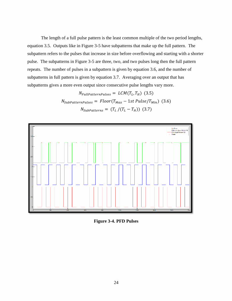
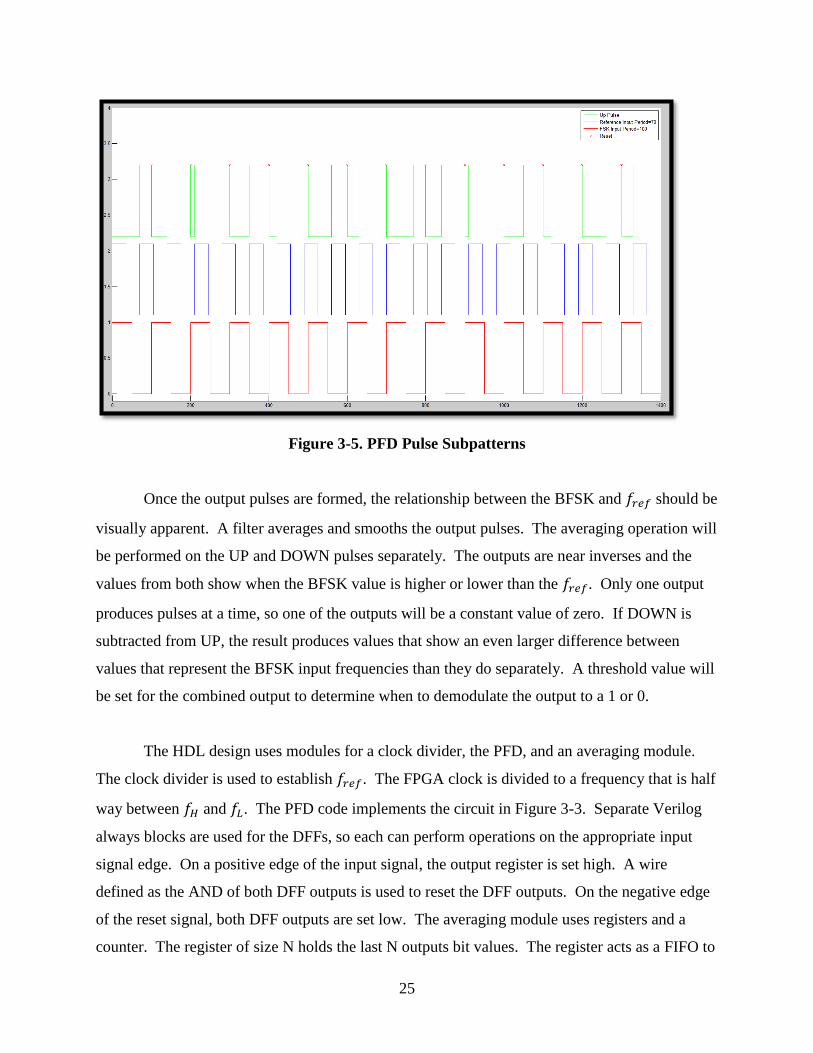
The length of a full pulse pattern is the least common multiple of the two period lengths,
equation 3.5. Outputs like in Figure 3-5 have subpatterns that make up the full pattern. The
subpattern refers to the pulses that increase in size before overflowing and starting with a shorter
pulse. The subpatterns in Figure 3-5 are three, two, and two pulses long then the full pattern
repeats. The number of pulses in a subpattern is given by equation 3.6, and the number of
subpatterns in full pattern is given by equation 3.7. Averaging over an output that has
subpatterns gives a more even output since consecutive pulse lengths vary more.
𝑁𝐹𝑢𝑙𝑙𝑃𝑎𝑡𝑡𝑒𝑟𝑛𝑃𝑢𝑙𝑠𝑒𝑠 = 𝐿𝐶𝑀(𝑇𝐿 , 𝑇𝐻) (3.5)
𝑁𝑆𝑢𝑏𝑃𝑎𝑡𝑡𝑒𝑟𝑛𝑃𝑢𝑙𝑠𝑒𝑠 = 𝐹𝑙𝑜𝑜𝑟(𝑇𝑀𝑎𝑥 − 1𝑠𝑡 𝑃𝑢𝑙𝑠𝑒/𝑇𝑀𝑖𝑛) (3.6)
𝑁𝑆𝑢𝑏𝑃𝑎𝑡𝑡𝑒𝑟𝑛𝑠 = (𝑇𝐿 /(𝑇𝐿 − 𝑇𝐻)) (3.7)
Figure 3-4. PFD Pulses
25
Figure 3-5. PFD Pulse Subpatterns
Once the output pulses are formed, the relationship between the BFSK and 𝑓𝑟𝑒𝑓 should be
visually apparent. A filter averages and smooths the output pulses. The averaging operation will
be performed on the UP and DOWN pulses separately. The outputs are near inverses and the
values from both show when the BFSK value is higher or lower than the 𝑓𝑟𝑒𝑓. Only one output
produces pulses at a time, so one of the outputs will be a constant value of zero. If DOWN is
subtracted from UP, the result produces values that show an even larger difference between
values that represent the BFSK input frequencies than they do separately. A threshold value will
be set for the combined output to determine when to demodulate the output to a 1 or 0.
The HDL design uses modules for a clock divider, the PFD, and an averaging module.
The clock divider is used to establish 𝑓𝑟𝑒𝑓. The FPGA clock is divided to a frequency that is half
way between 𝑓𝐻 and 𝑓𝐿. The PFD code implements the circuit in Figure 3-3. Separate Verilog
always blocks are used for the DFFs, so each can perform operations on the appropriate input
signal edge. On a positive edge of the input signal, the output register is set high. A wire
defined as the AND of both DFF outputs is used to reset the DFF outputs. On the negative edge
of the reset signal, both DFF outputs are set low. The averaging module uses registers and a
counter. The register of size N holds the last N outputs bit values. The register acts as a FIFO to
26
shift the bits in and out. The counter increments when a 1 is shifted in and decrements if a 1 is
shifted out to keep a running count of the number of 1’s over the most recent n bits. The
simulated output used N = 1000.
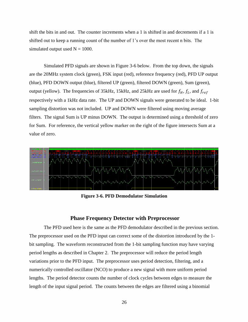
Simulated PFD signals are shown in Figure 3-6 below. From the top down, the signals
are the 20MHz system clock (green), FSK input (red), reference frequency (red), PFD UP output
(blue), PFD DOWN output (blue), filtered UP (green), filtered DOWN (green), Sum (green),
output (yellow). The frequencies of 35kHz, 15kHz, and 25kHz are used for 𝑓𝐻, 𝑓𝐿, and 𝑓𝑟𝑒𝑓
respectively with a 1kHz data rate. The UP and DOWN signals were generated to be ideal. 1-bit
sampling distortion was not included. UP and DOWN were filtered using moving average
filters. The signal Sum is UP minus DOWN. The output is determined using a threshold of zero
for Sum. For reference, the vertical yellow marker on the right of the figure intersects Sum at a
value of zero.
Figure 3-6. PFD Demodulator Simulation
Phase Frequency Detector with Preprocessor
The PFD used here is the same as the PFD demodulator described in the previous section.
The preprocessor used on the PFD input can correct some of the distortion introduced by the 1-
bit sampling. The waveform reconstructed from the 1-bit sampling function may have varying
period lengths as described in Chapter 2. The preprocessor will reduce the period length
variations prior to the PFD input. The preprocessor uses period detection, filtering, and a
numerically controlled oscillator (NCO) to produce a new signal with more uniform period
lengths. The period detector counts the number of clock cycles between edges to measure the
length of the input signal period. The counts between the edges are filtered using a binomial
27
filter to provide a more consistent output frequency [12]. The NCO generates a new waveform
using the filtered value to set the period length. The block diagram of the preprocessor is shown
below in Figure 3-7. All three of the blocks in the preprocessor can be implemented in hardware
using few resources on a FPGA.
Figure 3-7. PFD Preprocessor
The HDL design uses modules for each of the pre-processor blocks. The period detector
is similar to the Counter demodulator without the accumulator. A binomial filter is used to
average the pulse lengths and provide a value to the NCO. The NCO produces a new BFSK
input that is passed to the PFD.
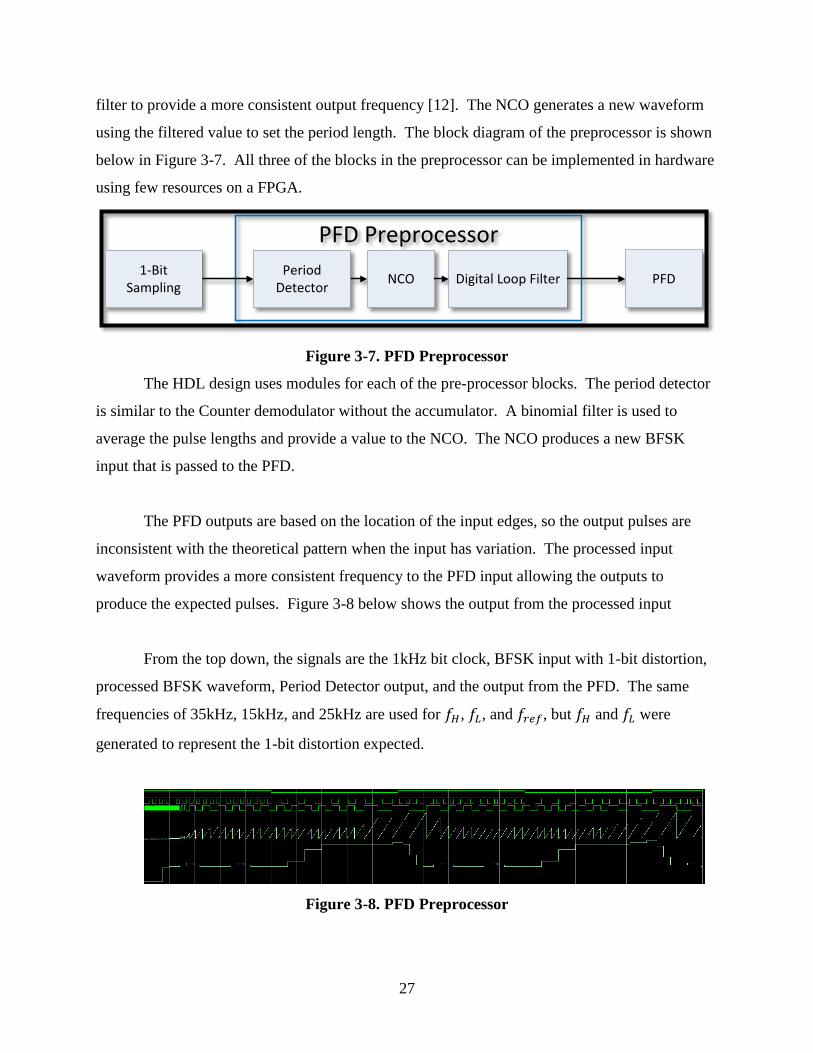
The PFD outputs are based on the location of the input edges, so the output pulses are
inconsistent with the theoretical pattern when the input has variation. The processed input
waveform provides a more consistent frequency to the PFD input allowing the outputs to
produce the expected pulses. Figure 3-8 below shows the output from the processed input
From the top down, the signals are the 1kHz bit clock, BFSK input with 1-bit distortion,
processed BFSK waveform, Period Detector output, and the output from the PFD. The same
frequencies of 35kHz, 15kHz, and 25kHz are used for 𝑓𝐻, 𝑓𝐿, and 𝑓𝑟𝑒𝑓, but 𝑓𝐻 and 𝑓𝐿 were
generated to represent the 1-bit distortion expected.
Figure 3-8. PFD Preprocessor
PFD Preprocessor
Digital Loop FilterNCO PFDPeriod
Detector1-Bit
Sampling

28
Chapter 4 - Demodulator Comparison Tests
Power Consumption
Power consumption on the Microsemi Igloo FPGA’s are directly related to the size of the
design and the frequencies used in the design [2, 14]. Amsler shows the power consumption
trends almost linearly with both parameters. Libero, the Microsemi Integrated Development
Environment (IDE), allows the size of the design to be viewed after the files are compiled and
the layout run. The layout was optimized in Libero minimize timing and power consumption.
The estimated power usage can be viewed with the Smart Power feature in Libero. The Smart
Power calculations are typically slightly low compared to observed power, but the values do
provide a good approximation [2]. Smart Power also gives an approximate battery life based on
a given battery size for the design. The battery life does not always follow with the size of the
design. The actual power usage will vary based on several factor including, the exact FPGA
used, the voltages used on the FPGA, and the clock frequencies used to run each module. These
values do provide a good means of comparison of the demodulator designs because all power
approximations will use the same factors except for the demodulator design.
Size of Design
The size of the design can be measured within Smart Power. The design size of the
AGLN250 FPGA on the development board used for this project can be measured by the number
of flip-flops (FF) used. The AGLN250 has 6144. The FPGA uses components other than FFs,
but the number of FFs used provides a good indicator of design size.
A simpler design can lead to a smaller design. The Counter was the simplest design
discussed in this paper and produced the smallest FPGA design. The Counter used 356 of 6144
FFs. The simplicity and size are the greatest advantages to the Counter. The downside of the
design is that its functionality is very dependent on the clock frequency. The design can be
slowed, but the reaction time of the Counter will also be slowed meaning it will not work at
higher data rates. As expected, the more complicated designs required increased FPGA
resources to implement. The One-Shot, PFD, and PFD with preprocessor used 269, 2574, 3066
FFs respectively.
29
Power
Ultimately, the power consumption and battery life are the most important factors.
Design size and frequency contribute to the power, but the primary figure of merit must be
power consumption. Using as little power as possible and extending battery life is the most
important factor. The battery life calculations were found using Smart Power assuming a
100mAh battery. The power and battery life for each demodulator are shown in Table 4-1.
Demodulator Power (mW) Design Size
(FFs)
Active Time (hr) per
100mAh Battery
Counter 0.30 356 398
One-Shot 0.54 269 222
PFD
PFD w/preproc
6.10
6.69
2574
3066
19.7
17.9
Table 4-1. Demodulator Power Consumption
Again, these values do not exactly reflect how the demodulators will perform on any
given system. The power measurements are approximations made with several assumptions, but
because these values were all found using the same set-up, the measurements can be useful for
comparing the demodulators.
Error Analysis
The demodulator performance in a system must also be evaluated when noise is present
together with the signal. The noise performance was evaluated using random input data. Errors
are projected on top of the data. The errors invert the input causing the BFSK signal to use the
incorrect frequency. A random number of errors, from 1 to 5, with random lengths, up to 𝑇𝑏
were projected onto the input. The total of the errors covered between 0.1% and 10% of the
input. The induced error inverted the logic level of the input causing the opposite IF BFSK
frequency to be used. The outputs of the demodulators were checked to see how many of the
errant bit decision were made by each demodulator compared to the error free input. MATLAB
was used to simulate 10,000 inputs with errors. The outputs were plotted with the error percent
on the x-axis and the number of errors in the demodulated output on the y-axis. To better view
30
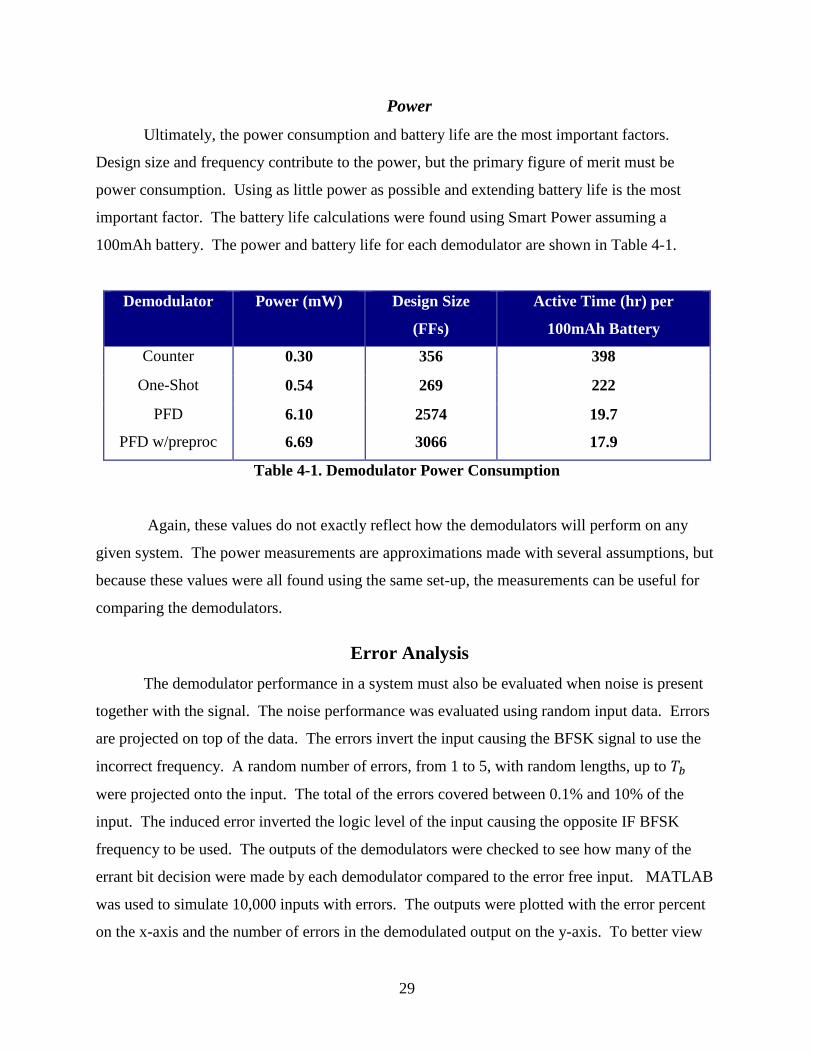
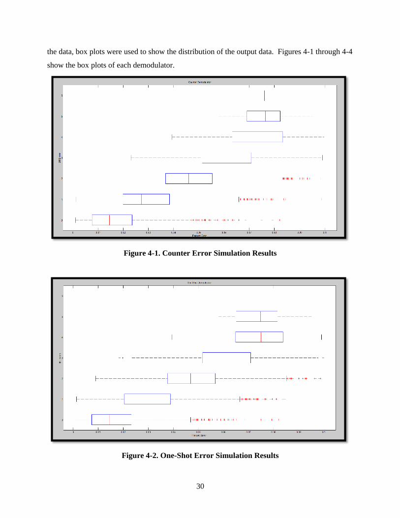
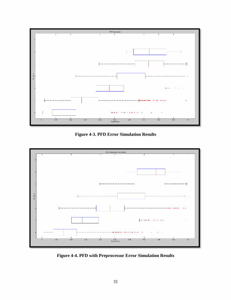
the data, box plots were used to show the distribution of the output data. Figures 4-1 through 4-4
show the box plots of each demodulator.
Figure 4-1. Counter Error Simulation Results
Figure 4-2. One-Shot Error Simulation Results
31
Figure 4-3. PFD Error Simulation Results
Figure 4-4. PFD with Preprocessor Error Simulation Results
32
Each of the demodulators has very similar error box plots. The total number of errors over the
10,000 simulations was accumulated for each demodulator. Those results are shown in Table 4-
2 below. From this error analysis, all of the demodulators are nearly equivalent for this setup of
𝑓𝐻, 𝑓𝐿, 𝑓𝑠, and 𝑇𝑏.
Demodulator Total Simulation Errors
Counter 13576
One-Shot 13295
Phase-Frequency Detector 13384
Phase Frequency Detector w/Preprocessor 13365
Table 4-2 Error Simulation Results
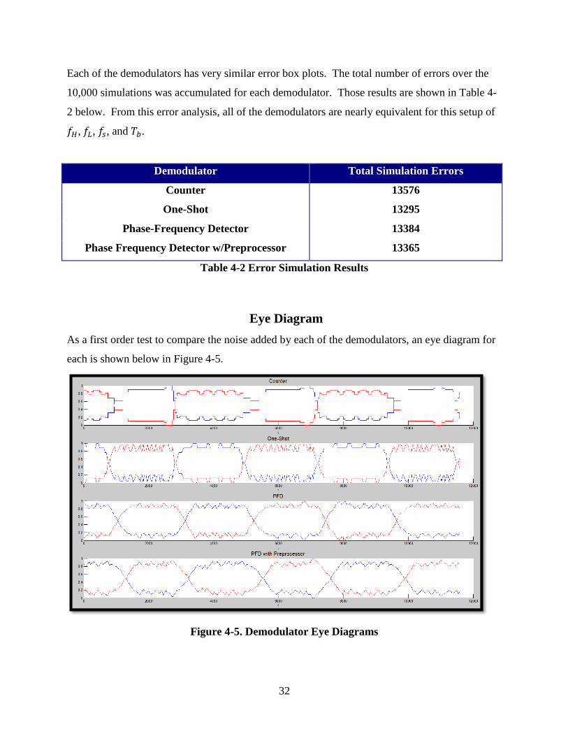
Eye Diagram
As a first order test to compare the noise added by each of the demodulators, an eye diagram for
each is shown below in Figure 4-5.
Figure 4-5. Demodulator Eye Diagrams
33
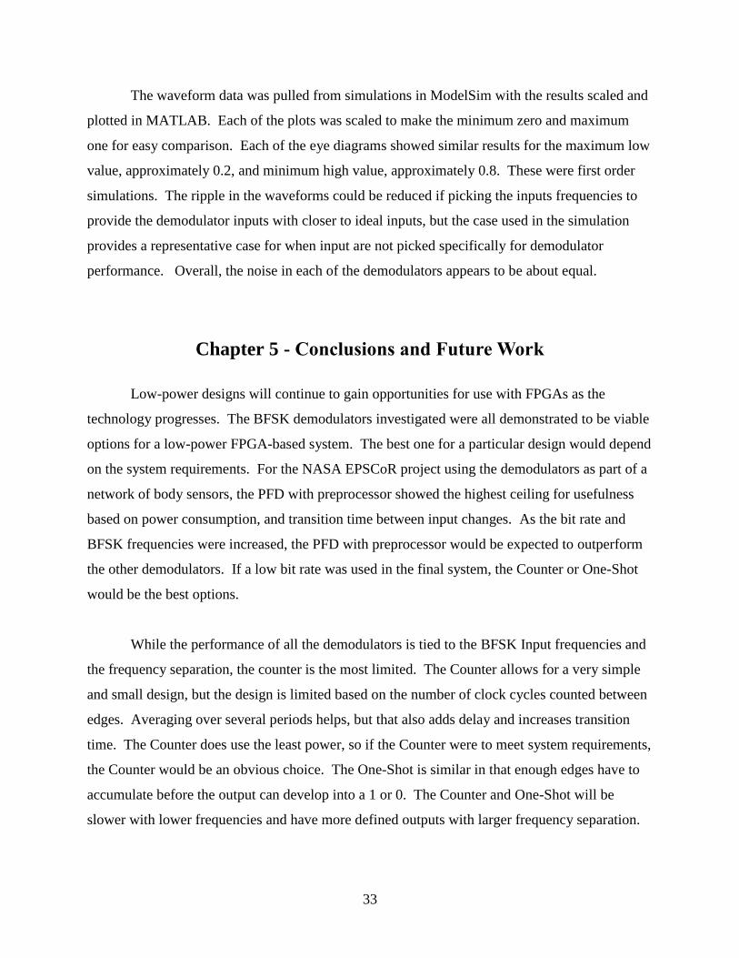
The waveform data was pulled from simulations in ModelSim with the results scaled and
plotted in MATLAB. Each of the plots was scaled to make the minimum zero and maximum
one for easy comparison. Each of the eye diagrams showed similar results for the maximum low
value, approximately 0.2, and minimum high value, approximately 0.8. These were first order
simulations. The ripple in the waveforms could be reduced if picking the inputs frequencies to
provide the demodulator inputs with closer to ideal inputs, but the case used in the simulation
provides a representative case for when input are not picked specifically for demodulator
performance. Overall, the noise in each of the demodulators appears to be about equal.
Chapter 5 - Conclusions and Future Work
Low-power designs will continue to gain opportunities for use with FPGAs as the
technology progresses. The BFSK demodulators investigated were all demonstrated to be viable
options for a low-power FPGA-based system. The best one for a particular design would depend
on the system requirements. For the NASA EPSCoR project using the demodulators as part of a
network of body sensors, the PFD with preprocessor showed the highest ceiling for usefulness
based on power consumption, and transition time between input changes. As the bit rate and
BFSK frequencies were increased, the PFD with preprocessor would be expected to outperform
the other demodulators. If a low bit rate was used in the final system, the Counter or One-Shot
would be the best options.
While the performance of all the demodulators is tied to the BFSK Input frequencies and
the frequency separation, the counter is the most limited. The Counter allows for a very simple
and small design, but the design is limited based on the number of clock cycles counted between
edges. Averaging over several periods helps, but that also adds delay and increases transition
time. The Counter does use the least power, so if the Counter were to meet system requirements,
the Counter would be an obvious choice. The One-Shot is similar in that enough edges have to
accumulate before the output can develop into a 1 or 0. The Counter and One-Shot will be
slower with lower frequencies and have more defined outputs with larger frequency separation.
34
The PFD, with or without the preprocessing, is also dependent on the input frequencies,
but as soon as an edge occurs, an output pulse is started. The output still needs to be filtered, but
less transition time in the PFD is needed before changing between UP and DOWN output pulses.
Once the BFSK input changes, the output pulse reflect the change.
If the frequencies out of the 1-bit sampling could be picked to optimize the BFSK input
into the PFD, the performance could increase and the preprocessor may not be needed. With the
right frequencies, the averaging could be reduced or eliminated, the transition time could be
reduced, and the ripple in the output pulses could be reduced. Those improvements would lead
to higher data rate capability, less delay, decrease in design size, and decreased power
consumption.
This study was mainly comparing the demodulator designs, but several steps could be
taken to minimize the power consumption once a design is selected. Reducing every register to
the bare minimum size would reduce the static and dynamic power usage. Synthesis of the HDL
design should remove unneeded parts or registers, but changing the design directly would be
cleaner and less ambiguous if a question of logic operation were to arise. Reducing every clock
rate as much as possible would be the next step. Internal clocks could likely be reduced with no
harmful effect on the demodulated output. Writing efficient code to perform operations in
parallel could be another option to reduce time and power. The HDL designs all used non-
blocking statements which may take more time resulting in more power usage. Every bit of
improvement helps when considering low-power designs especially when the power may rely
solely on an energy harvesting solution.
The input frequency could even be manipulated in a different way. There are several
frequencies that are important to the design. The clock frequency will play a large part in how
much power the design uses and also the data rate that the design can demodulate. The BFSK
frequencies will play a part in the bandwidth of the signal, the ease of demodulating the under-
sampled signal, and influence the maximum data rate that can be used. The data rate, 𝑅𝑏, must
be a much lower frequency than 𝑓𝐿. In order to detect the frequency, several cycles of 𝑓𝐿 must be
present for the demodulator to measure. If 𝑓𝐿was 20kHz and the data rate was 10kHz, 𝑓𝐿 would
35
only have time for two cycles before the BFSK Input would change back to 𝑓𝐻. That is not
enough for the demodulators to make a good measurement. A first order rule of thumb could be
for the data rate to be an order of magnitude lower than 𝑓𝐿.
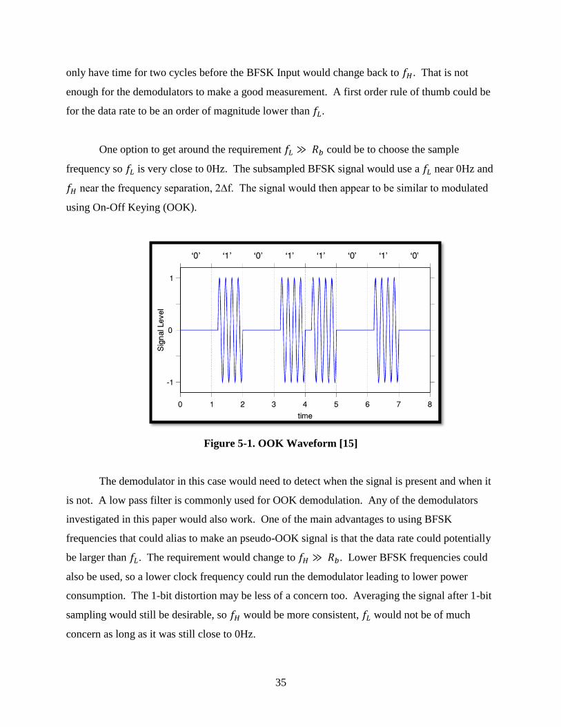
One option to get around the requirement 𝑓𝐿 ≫ 𝑅𝑏 could be to choose the sample
frequency so 𝑓𝐿 is very close to 0Hz. The subsampled BFSK signal would use a 𝑓𝐿 near 0Hz and
𝑓𝐻 near the frequency separation, 2∆f. The signal would then appear to be similar to modulated
using On-Off Keying (OOK).
Figure 5-1. OOK Waveform [15]
The demodulator in this case would need to detect when the signal is present and when it
is not. A low pass filter is commonly used for OOK demodulation. Any of the demodulators
investigated in this paper would also work. One of the main advantages to using BFSK
frequencies that could alias to make an pseudo-OOK signal is that the data rate could potentially
be larger than 𝑓𝐿. The requirement would change to 𝑓𝐻 ≫ 𝑅𝑏. Lower BFSK frequencies could
also be used, so a lower clock frequency could run the demodulator leading to lower power
consumption. The 1-bit distortion may be less of a concern too. Averaging the signal after 1-bit
sampling would still be desirable, so 𝑓𝐻 would be more consistent, 𝑓𝐿 would not be of much
concern as long as it was still close to 0Hz.

36
The clock frequency used in the design will not need to be as high as the board clock in
most cases. The frequency needed will depend partly on the FSK frequencies used and the data
rate. The Counter may need to be run with a faster clock for the design to work better. The One-
Shot and PFD may be able to run on a slower clock.
Regardless of the frequencies or the type of demodulator used, low-power systems
implemented on Field Programmable Gate Arrays (FPGA) have become more practical with
advancements leading to decreases in FPGA cost, power consumption, and physical size. In
systems that may need to operate for an extended time independent from a central power source,
low-power FPGA’s are a reasonable option. Combined with research into energy harvesting
solutions, a FPGA-based system could operate independently indefinitely.
37
References
[1] B. Lathi, Modern Digital and Analog Communication Systems, 3rd
ed, New York:
Oxford University Press, 1998.
[2] C. Amsler, “The Effects of Hardware Acceleration on Power Usage in Basic High-
Performance Computing,” M.S. thesis, Dept Elec. and Comp. Eng., Kansas State Univ.,
2010.
[3] J. Meyer, “Modeling Phase-Locked Loops Using Verilog.” 39th
Annual Precise Time
and Time Interval (PTTI) Meeting, 2007 [Online]. Available:
http://www.dtic.mil/dtic/tr/fulltext/u2/a483891.pdf
[4] “Fundamentals of Phase Locked Loops (PLLs).” [Online]. Available:
http://www.analog.com/media/en/training-seminars/tutorials/MT-086.pdf
[5] “Behavioral Modeling of PLL Using Verilog-A.” [Online]. Available:
http://www.silvaco.com/tech_lib_TCAD/simulationstandard/2003/jul/a2/july2003_a2.pdf
[6] W Kester, “Undersampling Applications” [Online]. Available:
http://www.analog.com/static/imported-files/seminars_webcasts
/3689418379346Section5.pdf
[7] D. Lockhart, “What You Really Need to Know About Sample Rate.” [Online].
Available:
http://www.dataq.com/support/documentation/pdf/article_pdfs/sample-rate.pdf
[8] M Kostic, “Sampling and Aliasing: An Interactive and On-Line Virtual Experiment.”
[Online]. Available:
https://www.ni.com/pdf/academic/us/journals/sampling_and_aliasing.pdf
[9] R. Lyons, Understanding Digital Signal Processing, 3rd
ed, New Jersey: Prentice Hall,
2010.
[10] “Folding Diagram for Aliasing Calculations.” [Online]. Available:
http://www.mne.psu.edu/cimbala/me345/Exams/Folding_diagram_for_aliasing.pdf
[11] W. Kuhn, N. E. Lay, and et al, “A Microtransceiver for UHF Proximity Links
Including Mars Surface-to-Orbit Applications,” in Proc. of the IEEE, vol. 95, no 10, pp.
2019-2044, 2007.
38
[12] R. A. Haddad “A Class of Orthongonal Nonrecursive Binomial Filters,” in Proc of the
IEEE, vol. Au-19, no 4, pp. 296-304.
[13] X. Zhang, “VHF & UHF Energy Harvesting Radio System Phisical and MAC Layer
Considerations,” M.S. thesis, Dept Elec. and Comp. Eng., Kansas State Univ, 2001.
[14] Microsemi. “Dynamic Power Reduction in Flash FPGAs.” [Online]. Available:
[15] “Digital Modulation one bit at a time.” [Online]. Available:
https://www.st-andrews.ac.uk/~www_pa/Scots_Guide/RadCom/part19/page1.html
39
Appendix A – Hardware Design Language (HDL), Verilog Code
Counter
// Counter_all.v
/////////////////////////////////////////////////////////////////
// Riley Harrington
// Kansas State University
// Electrical and Computer Engineering
// This file contains the modules used in the Counter BFSK
// demodulator.
// Modules:
// -Counter
// -Edge Detector
/////////////////////////////////////////////////////////////////
`timescale 1ps / 1ps
// Counter Module
module Counter_all(clk, ar, SigIn, SigOut);
// inputs
input clk;
input ar;
input SigIn;
// outputs
output wire SigOut;
// end module I/O
// Parameters
parameter CountSize = 20;
parameter RegSize = 15;
parameter Ref_clock = 2;
// For a clock frequency of 20MHz and FSK frequencies of 15kHz and 35kHz,
// the count value will be between 5333 for 15kHz and 2286 for 35kHz.
// Thoase numbers are found by dividing the clock frequency by the FSK
// frequency then multiplying the result by four since the four cycles are
// accumulated before setting the value to Count.
// 20MHz/15kHz = 1333.3 --> 1333.3*4=5333
// 20MHz/35kHz = 571.43 --> 571.43*4=2286
// The mid-point between the numbers is ~3800
parameter Threshold = 180;//3800;
// end parameters
// Registers
reg [20:0] OutputCount, CountUp;
reg AvgOut;
reg [RegSize-1:0] S4, S3, S23, S34, S123, S234, S1234, Sout;
// end registers
// Wires & assignments
wire EdgeP, EdgeN;
wire Edges;
wire ref_clk;
assign Edges = EdgeP || EdgeN;
assign SigOut = (Sout > Threshold)? 1'b1:1'b0;
// end wires
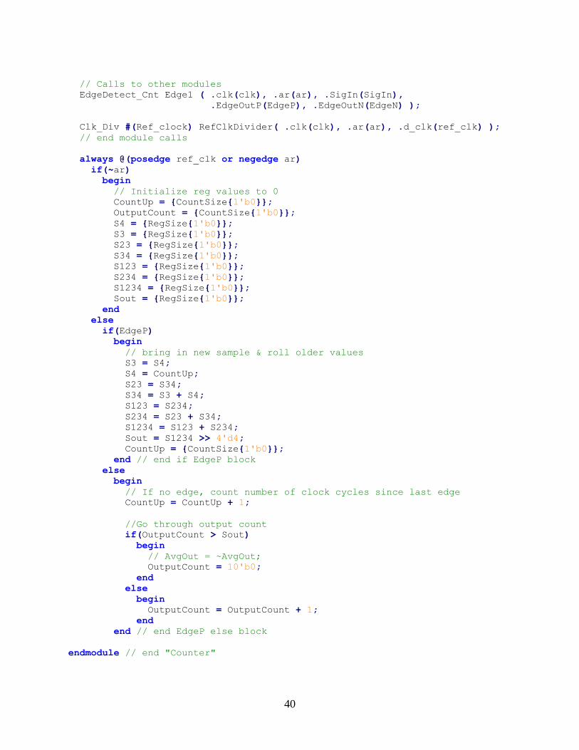
40
// Calls to other modules
EdgeDetect_Cnt Edge1 ( .clk(clk), .ar(ar), .SigIn(SigIn),
.EdgeOutP(EdgeP), .EdgeOutN(EdgeN) );
Clk_Div #(Ref_clock) RefClkDivider( .clk(clk), .ar(ar), .d_clk(ref_clk) );
// end module calls
always @(posedge ref_clk or negedge ar)
if(~ar)
begin
// Initialize reg values to 0
CountUp = {CountSize{1'b0}};
OutputCount = {CountSize{1'b0}};
S4 = {RegSize{1'b0}};
S3 = {RegSize{1'b0}};
S23 = {RegSize{1'b0}};
S34 = {RegSize{1'b0}};
S123 = {RegSize{1'b0}};
S234 = {RegSize{1'b0}};
S1234 = {RegSize{1'b0}};
Sout = {RegSize{1'b0}};
end
else
if(EdgeP)
begin
// bring in new sample & roll older values
S3 = S4;
S4 = CountUp;
S23 = S34;
S34 = S3 + S4;
S123 = S234;
S234 = S23 + S34;
S1234 = S123 + S234;
Sout = S1234 >> 4'd4;
CountUp = {CountSize{1'b0}};
end // end if EdgeP block
else
begin
// If no edge, count number of clock cycles since last edge
CountUp = CountUp + 1;
//Go through output count
if(OutputCount > Sout)
begin
// AvgOut = ~AvgOut;
OutputCount = 10'b0;
end
else
begin
OutputCount = OutputCount + 1;
end
end // end EdgeP else block
endmodule // end "Counter"
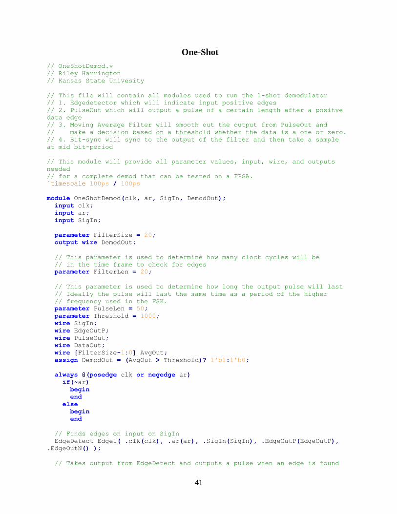
41
One-Shot
// OneShotDemod.v
// Riley Harrington
// Kansas State Univesity
// This file will contain all modules used to run the 1-shot demodulator
// 1. Edgedetector which will indicate input positive edges
// 2. PulseOut which will output a pulse of a certain length after a positve
data edge
// 3. Moving Average Filter will smooth out the output from PulseOut and
// make a decision based on a threshold whether the data is a one or zero.
// 4. Bit-sync will sync to the output of the filter and then take a sample
at mid bit-period
// This module will provide all parameter values, input, wire, and outputs
needed
// for a complete demod that can be tested on a FPGA.
`timescale 100ps / 100ps
module OneShotDemod(clk, ar, SigIn, DemodOut);
input clk;
input ar;
input SigIn;
parameter FilterSize = 20;
output wire DemodOut;
// This parameter is used to determine how many clock cycles will be
// in the time frame to check for edges
parameter FilterLen = 20;
// This parameter is used to determine how long the output pulse will last
// Ideally the pulse will last the same time as a period of the higher
// frequency used in the FSK.
parameter PulseLen = 50;
parameter Threshold = 1000;
wire SigIn;
wire EdgeOutP;
wire PulseOut;
wire DataOut;
wire [FilterSize-1:0] AvgOut;
assign DemodOut = (AvgOut > Threshold)? 1'b1:1'b0;
always @(posedge clk or negedge ar)
if(~ar)
begin
end
else
begin
end
// Finds edges on input on SigIn
EdgeDetect Edge1( .clk(clk), .ar(ar), .SigIn(SigIn), .EdgeOutP(EdgeOutP),
.EdgeOutN() );
// Takes output from EdgeDetect and outputs a pulse when an edge is found
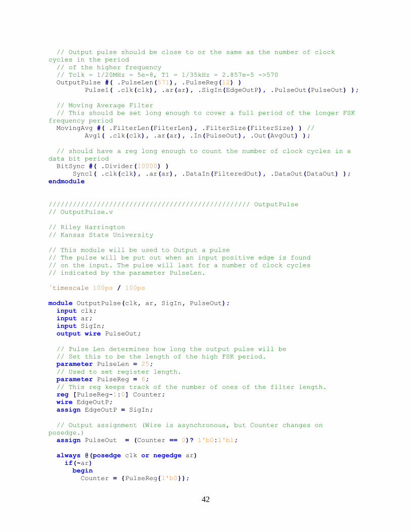
42
// Output pulse should be close to or the same as the number of clock
cycles in the period
// of the higher frequency
// Tclk = 1/20MHz = 5e-8, T1 = 1/35kHz = 2.857e-5 ->570
OutputPulse #( .PulseLen(571), .PulseReg(12) )
Pulse1( .clk(clk), .ar(ar), .SigIn(EdgeOutP), .PulseOut(PulseOut) );
// Moving Average Filter
// This should be set long enough to cover a full period of the longer FSK
frequency period
MovingAvg #( .FilterLen(FilterLen), .FilterSize(FilterSize) ) //
Avg1( .clk(clk), .ar(ar), .In(PulseOut), .Out(AvgOut) );
// should have a reg long enough to count the number of clock cycles in a
data bit period
BitSync #( .Divider(10000) )
Sync1( .clk(clk), .ar(ar), .DataIn(FilteredOut), .DataOut(DataOut) );
endmodule
////////////////////////////////////////////////// OutputPulse
// OutputPulse.v
// Riley Harrington
// Kansas State University
// This module will be used to Output a pulse
// The pulse will be put out when an input positive edge is found
// on the input. The pulse will last for a number of clock cycles
// indicated by the parameter PulseLen.
`timescale 100ps / 100ps
module OutputPulse(clk, ar, SigIn, PulseOut);
input clk;
input ar;
input SigIn;
output wire PulseOut;
// Pulse Len determines how long the output pulse will be
// Set this to be the length of the high FSK period.
parameter PulseLen = 25;
// Used to set register length.
parameter PulseReg = 6;
// This reg keeps track of the number of ones of the filter length.
reg [PulseReg-1:0] Counter;
wire EdgeOutP;
assign EdgeOutP = SigIn;
// Output assignment (Wire is asynchronous, but Counter changes on
posedge.)
assign PulseOut = (Counter == 0)? 1'b0:1'b1;
always @(posedge clk or negedge ar)
if(~ar)
begin
Counter = {PulseReg{1'b0}};
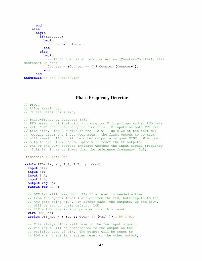
43
end
else
begin
if(EdgeOutP)
begin
Counter = PulseLen;
end
else
begin
// If Counter is at zero, no action (Counter=Counter), else
decrement Counter
Counter = (Counter == 0)? Counter:(Counter-1);
end
end
endmodule // end OutputPulse
Phase Frequency Detector
// PFD.v
// Riley Harrington
// Kansas State University
// Phase-Frequency Detector (PFD)
// PFD based on digital circuit using two D flip-flops and an AND gate
// with "UP" and "DOWN" outputs from DFFs. D inputs on both FFs are
// tied high. The Q output of the FFs will go HIGH at the next clk
// posedge after the input goes HIGH. The first output to go HIGH
// will remain HIGH until the other output also goes HIGH. When both
// outputs are HIGH, the AND gate will reset the FF outputs.
// The UP and DOWN outputs indicate whether the input signal frequency
// (InA) is higher or lower than the reference frequency (InB).
`timescale 100ps/100ps
module PFD(clk, ar, InA, InB, up, down);
input clk;
input ar;
input InA;
input InB;
output reg up;
output reg down;
// DFF_Rst will reset both FFs if a reset is needed either
// from the system level (~ar) or from the PFD, both inputs to the
// AND gate being HIGH. In either case, the outputs, up and down,
// will be set to their default, LOW.
// **The AND gate is incorporated into this reset
wire DFF_Rst;
assign DFF_Rst = ( (up && down) || (~ar) )? 1'b0:1'b1;
// This always block will take in the InA input signal.
// The input will be transferred to the output on the
// positive edge of clk. The output will be reset to
// LOW when there is a system reset or the other output,
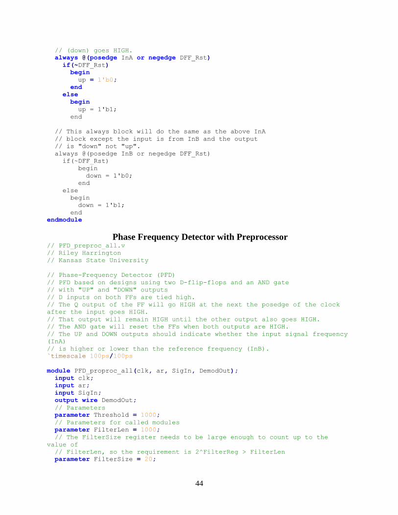
44
// (down) goes HIGH.
always @(posedge InA or negedge DFF_Rst)
if(~DFF_Rst)
begin
up = 1'b0;
end
else
begin
up = 1'b1;
end
// This always block will do the same as the above InA
// block except the input is from InB and the output
// is "down" not "up".
always @(posedge InB or negedge DFF_Rst)
if(~DFF_Rst)
begin
down = 1'b0;
end
else
begin
down = 1'b1;
end
endmodule
Phase Frequency Detector with Preprocessor // PFD_preproc_all.v
// Riley Harrington
// Kansas State University
// Phase-Frequency Detector (PFD)
// PFD based on designs using two D-flip-flops and an AND gate
// with "UP" and "DOWN" outputs
// D inputs on both FFs are tied high.
// The Q output of the FF will go HIGH at the next the posedge of the clock
after the input goes HIGH.
// That output will remain HIGH until the other output also goes HIGH.
// The AND gate will reset the FFs when both outputs are HIGH.
// The UP and DOWN outputs should indicate whether the input signal frequency
(InA)
// is higher or lower than the reference frequency (InB).
`timescale 100ps/100ps
module PFD_proproc_all(clk, ar, SigIn, DemodOut);
input clk;
input ar;
input SigIn;
output wire DemodOut;
// Parameters
parameter Threshold = 1000;
// Parameters for called modules
parameter FilterLen = 1000;
// The FilterSize register needs to be large enough to count up to the
value of
// FilterLen, so the requirement is 2^FilterReg > FilterLen
parameter FilterSize = 20;
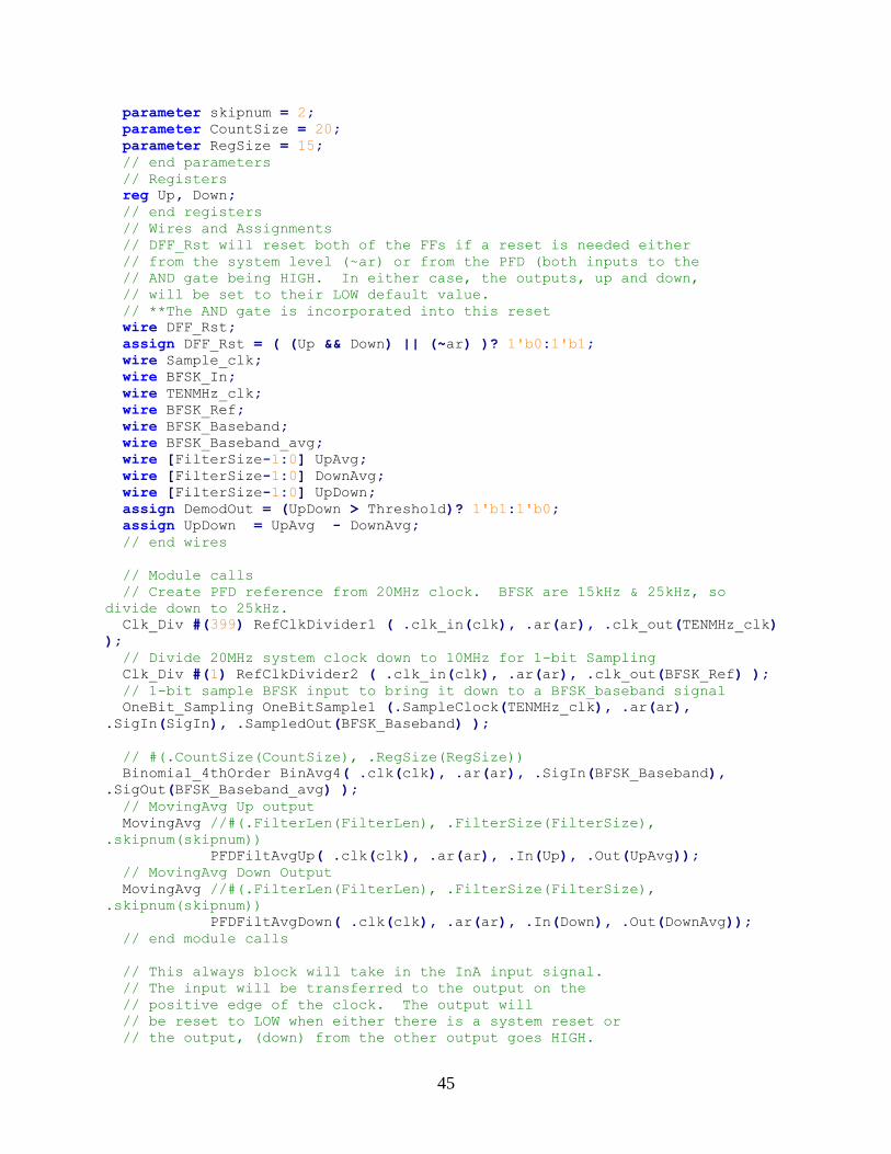
45
parameter skipnum = 2;
parameter CountSize = 20;
parameter RegSize = 15;
// end parameters
// Registers
reg Up, Down;
// end registers
// Wires and Assignments
// DFF_Rst will reset both of the FFs if a reset is needed either
// from the system level (~ar) or from the PFD (both inputs to the
// AND gate being HIGH. In either case, the outputs, up and down,
// will be set to their LOW default value.
// **The AND gate is incorporated into this reset
wire DFF_Rst;
assign DFF_Rst = ( (Up && Down) || (~ar) )? 1'b0:1'b1;
wire Sample_clk;
wire BFSK_In;
wire TENMHz_clk;
wire BFSK_Ref;
wire BFSK_Baseband;
wire BFSK_Baseband_avg;
wire [FilterSize-1:0] UpAvg;
wire [FilterSize-1:0] DownAvg;
wire [FilterSize-1:0] UpDown;
assign DemodOut = (UpDown > Threshold)? 1'b1:1'b0;
assign UpDown = UpAvg - DownAvg;
// end wires
// Module calls
// Create PFD reference from 20MHz clock. BFSK are 15kHz & 25kHz, so
divide down to 25kHz.
Clk_Div #(399) RefClkDivider1 ( .clk_in(clk), .ar(ar), .clk_out(TENMHz_clk)
);
// Divide 20MHz system clock down to 10MHz for 1-bit Sampling
Clk_Div #(1) RefClkDivider2 ( .clk_in(clk), .ar(ar), .clk_out(BFSK_Ref) );
// 1-bit sample BFSK input to bring it down to a BFSK_baseband signal
OneBit_Sampling OneBitSample1 (.SampleClock(TENMHz_clk), .ar(ar),
.SigIn(SigIn), .SampledOut(BFSK_Baseband) );
// #(.CountSize(CountSize), .RegSize(RegSize))
Binomial_4thOrder BinAvg4( .clk(clk), .ar(ar), .SigIn(BFSK_Baseband),
.SigOut(BFSK_Baseband_avg) );
// MovingAvg Up output
MovingAvg //#(.FilterLen(FilterLen), .FilterSize(FilterSize),
.skipnum(skipnum))
PFDFiltAvgUp( .clk(clk), .ar(ar), .In(Up), .Out(UpAvg));
// MovingAvg Down Output
MovingAvg //#(.FilterLen(FilterLen), .FilterSize(FilterSize),
.skipnum(skipnum))
PFDFiltAvgDown( .clk(clk), .ar(ar), .In(Down), .Out(DownAvg));
// end module calls
// This always block will take in the InA input signal.
// The input will be transferred to the output on the
// positive edge of the clock. The output will
// be reset to LOW when either there is a system reset or
// the output, (down) from the other output goes HIGH.
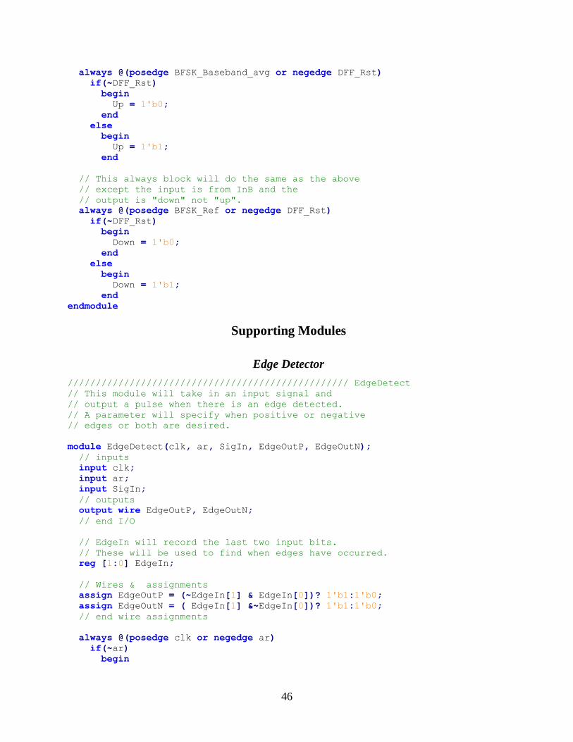
46
always @(posedge BFSK_Baseband_avg or negedge DFF_Rst)
if(~DFF_Rst)
begin
Up = 1'b0;
end
else
begin
Up = 1'b1;
end
// This always block will do the same as the above
// except the input is from InB and the
// output is "down" not "up".
always @(posedge BFSK_Ref or negedge DFF_Rst)
if(~DFF_Rst)
begin
Down = 1'b0;
end
else
begin
Down = 1'b1;
end
endmodule
Supporting Modules
Edge Detector
////////////////////////////////////////////////// EdgeDetect
// This module will take in an input signal and
// output a pulse when there is an edge detected.
// A parameter will specify when positive or negative
// edges or both are desired.
module EdgeDetect(clk, ar, SigIn, EdgeOutP, EdgeOutN);
// inputs
input clk;
input ar;
input SigIn;
// outputs
output wire EdgeOutP, EdgeOutN;
// end I/O
// EdgeIn will record the last two input bits.
// These will be used to find when edges have occurred.
reg [1:0] EdgeIn;
// Wires & assignments
assign EdgeOutP = (~EdgeIn[1] & EdgeIn[0])? 1'b1:1'b0;
assign EdgeOutN = ( EdgeIn[1] &~EdgeIn[0])? 1'b1:1'b0;
// end wire assignments
always @(posedge clk or negedge ar)
if(~ar)
begin
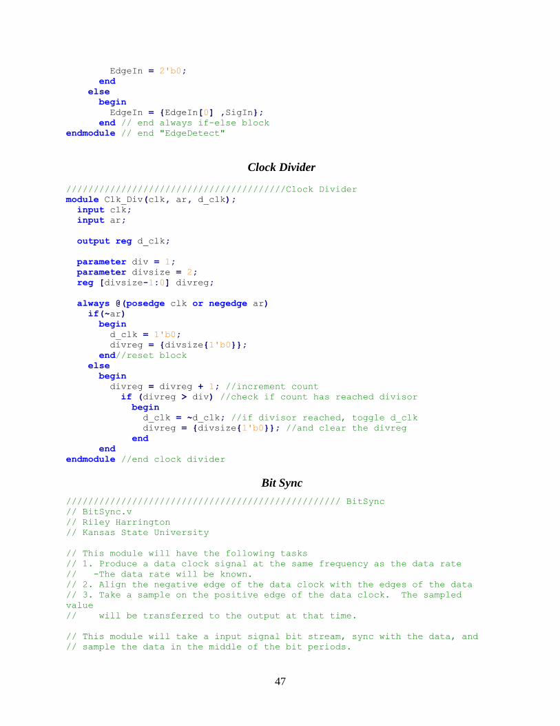
47
EdgeIn = 2'b0;
end
else
begin
EdgeIn = {EdgeIn[0] ,SigIn};
end // end always if-else block
endmodule // end "EdgeDetect"
Clock Divider
////////////////////////////////////////Clock Divider
module Clk_Div(clk, ar, d_clk);
input clk;
input ar;
output reg d_clk;
parameter div = 1;
parameter divsize = 2;
reg [divsize-1:0] divreg;
always @(posedge clk or negedge ar)
if(~ar)
begin
d_clk = 1'b0;
divreg = {divsize{1'b0}};
end//reset block
else
begin
divreg = divreg + 1; //increment count
if (divreg > div) //check if count has reached divisor
begin
d_clk = ~d_clk; //if divisor reached, toggle d_clk
divreg = {divsize{1'b0}}; //and clear the divreg
end
end
endmodule //end clock divider
Bit Sync
////////////////////////////////////////////////// BitSync
// BitSync.v
// Riley Harrington
// Kansas State University
// This module will have the following tasks
// 1. Produce a data clock signal at the same frequency as the data rate
// -The data rate will be known.
// 2. Align the negative edge of the data clock with the edges of the data
// 3. Take a sample on the positive edge of the data clock. The sampled
value
// will be transferred to the output at that time.
// This module will take a input signal bit stream, sync with the data, and
// sample the data in the middle of the bit periods.
48
// If there are mulitple of the same bits in a row, no data transition will
// be detected, so the sample clock will not be aligned in that perdiod.
// The negative edge will be lined up with the data edges and samples will be
// taken on the positive edges of the sample clock.
`timescale 100ps/100ps
// Data is independent.
// on system clock edges, check for data edges
// If data edge detected, align clock (reset)
// on data clock posedge, take sample
module BitSync(clk, ar, DataIn, DataOut);
input clk;
input ar;
input DataIn;
// output wire Sample;//probably doesn't need to be an output
output wire DataOut;
// SampledData will store the latest sample from the input.
reg SampledData;
// DataOut will reflect the latest sample from SampledData.
assign DataOut = SampledData;
// This reg will have the newest bit from the DataIn shifted in
// It will be used to find when data edges occur
reg [1:0] DataEdge;
// Divider should divide the system clock to generate a clock
// that is the same frequency as the data. (One cycle per data bit
period)
parameter Divider = 99;
wire DataClk;
wire RstDataClk;
assign RstDataClk = (DataEdge[1] != DataEdge[0])? 1'b0:1'b1;
// This will produce a data clock. Once the clock is aligned with the
data, the
// posedges, will indicate when to take a sample.
Clk_Div #( .div(Divider) ) DataClock ( .clk(clk), .ar(RstDataClk),
.d_clk(DataClk) );
// This takes the sample of DataIn and stores it in SampledData
// The output DataOut is assigned to SampledData, so the output reflects
the
// value of SampledData.
always @(posedge DataClk or negedge ar)
if(~ar)
begin
SampledData = 1'b0;
end
else
begin
SampledData = DataIn;
end
// This is used to detect when an edge of DataIn occurs.
// Those data edges are used to reset/align DataClk
always @(posedge clk or negedge ar)
begin
if(!ar)
begin
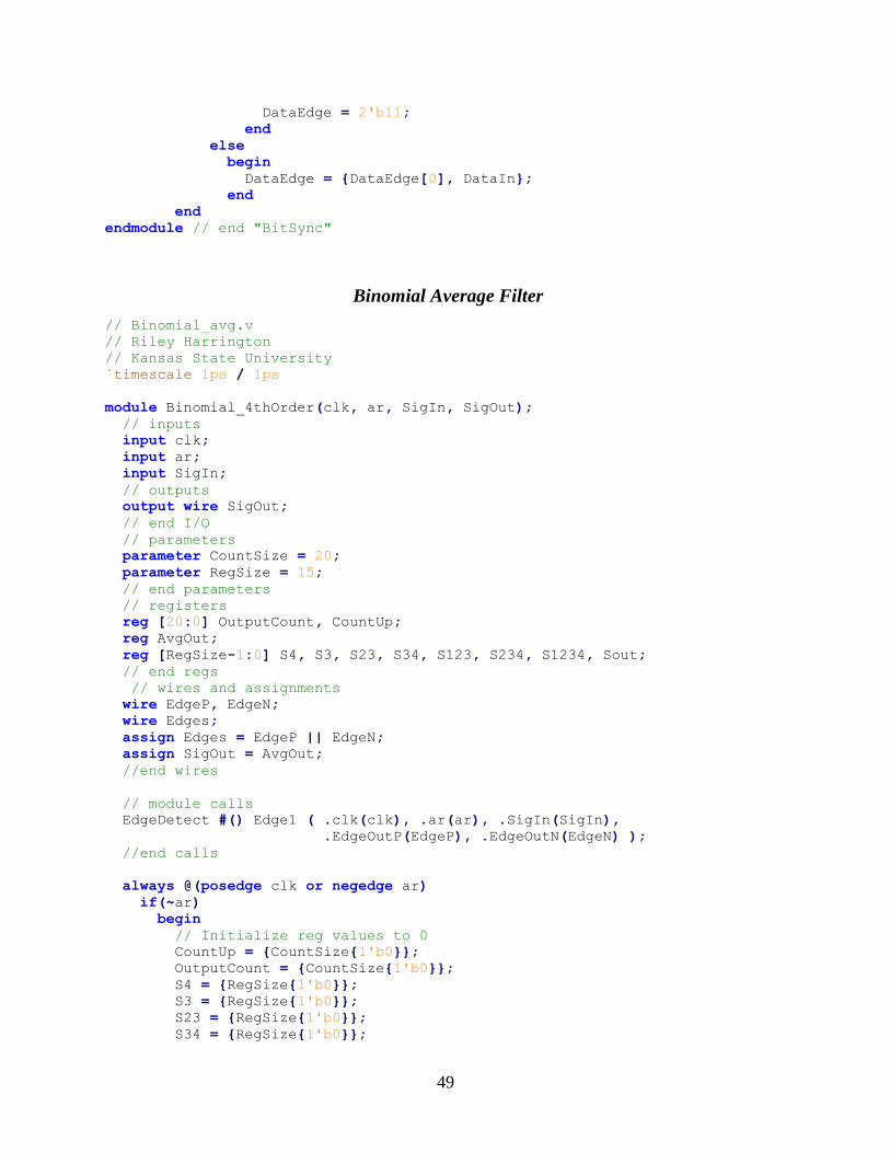
49
DataEdge = 2'b11;
end
else
begin
DataEdge = {DataEdge[0], DataIn};
end
end
endmodule // end "BitSync"
Binomial Average Filter
// Binomial_avg.v
// Riley Harrington
// Kansas State University
`timescale 1ps / 1ps
module Binomial_4thOrder(clk, ar, SigIn, SigOut);
// inputs
input clk;
input ar;
input SigIn;
// outputs
output wire SigOut;
// end I/O
// parameters
parameter CountSize = 20;
parameter RegSize = 15;
// end parameters
// registers
reg [20:0] OutputCount, CountUp;
reg AvgOut;
reg [RegSize-1:0] S4, S3, S23, S34, S123, S234, S1234, Sout;
// end regs
// wires and assignments
wire EdgeP, EdgeN;
wire Edges;
assign Edges = EdgeP || EdgeN;
assign SigOut = AvgOut;
//end wires
// module calls
EdgeDetect #() Edge1 ( .clk(clk), .ar(ar), .SigIn(SigIn),
.EdgeOutP(EdgeP), .EdgeOutN(EdgeN) );
//end calls
always @(posedge clk or negedge ar)
if(~ar)
begin
// Initialize reg values to 0
CountUp = {CountSize{1'b0}};
OutputCount = {CountSize{1'b0}};
S4 = {RegSize{1'b0}};
S3 = {RegSize{1'b0}};
S23 = {RegSize{1'b0}};
S34 = {RegSize{1'b0}};
50
S123 = {RegSize{1'b0}};
S234 = {RegSize{1'b0}};
S1234 = {RegSize{1'b0}};
Sout = {RegSize{1'b0}};
AvgOut = 1'b0;
end
else
begin
if(EdgeP)
begin
// bring in new sample & roll older values
S3 = S4;
S4 = CountUp;
S23 = S34;
S34 = S3 + S4;
S123 = S234;
S234 = S23 + S34;
S1234 = S123 + S234;
Sout = S1234 >> 4'd4;
CountUp = {CountSize{1'b0}};
end
else
begin
// If no edge, count number of clock cycles since last edge
CountUp = CountUp + 1;
//Go through output count
if(OutputCount > Sout)
begin
AvgOut = ~AvgOut;
OutputCount = 10'b0;
end
else
begin
OutputCount = OutputCount + 1;
end
end
end
endmodule
Moving Average Filter
////////////////////////////////////////////////// MovingAvg
// MovingAvg.v
// Riley Harrington
// Kansas State University
// This module separates a moving average filter into a separate module
// The module will add up the number of ones over a certain number of samples
// which is set by "FilterLen"
// SigIn has nearly constant pulses when the signal is at the higher FSK
frequency
// the signal will have intermittent pulses when the input is at the lower
FSK frequency.
51
// PFD_MovingAvg.v is the same as MovingAvg. with an extra input and
registers to handle
// a moving average operation on two signals at once. One of the resulting
Sum values
// is subtracted from the other to combine them into one signal. This worked
well for
// the particular situation this module was needed for where only one output
was desired.
`timescale 100ps / 100ps
module MovingAvg(clk, ar, In, Out);
// PARAMETERS or #define sections
//////////////////////////////////////////
// FilterLen is the length of the filter. FilterLen of bits will be summed
// to provide the moving average.
// It is easier to make this a power of two, so the divide needed for the
// average can use logical shift operation.
parameter FilterLen = 64;
// The FilterSize register needs to be large enough to count up to the
value of
// FilterLen, so the requirement is 2^FilterReg > FilterLen
parameter FilterSize = 7;
// END PARAMETERS
///////////////////////////////////////////////////////////
// I/O
/////////////////////////////////////////////////////////////////////
input clk;
input ar;
input In;
output wire [FilterSize-1:0] Out;
// End I/O
/////////////////////////////////////////////////////////////////
// REGISTERS
////////////////////////////////////////////////////////////////
// This register will hold the bits that will be summed
reg [FilterLen-1:0] FilterReg;
// This register will sum the values in the FilterReg.
// This reg will need to be large enough to count up to the length of
FilterLen
// 2^FilterReg > FilterLen
reg [FilterSize-1:0] FilterSum;
reg [FilterSize-1:0] skip;
parameter skipnum = 2;
// END REGISTERS
////////////////////////////////////////////////////////////
//assign Out = (FilterSum[FilterSize-1] == 0)? 1'b1:1'b0;
assign Out = FilterSum;
always @(posedge clk or negedge ar)
if(~ar)
begin
// Reset the registers to all zeros on a reset
FilterReg = {FilterLen{1'b0}};
FilterSum = {FilterSize{1'b0}};
skip = {FilterSize{1'b0}};
end
52
else
begin
// Four situations can happen
// 1. A zero is shifted in and a zero is shifted out
// 2. A one is shifted in and a one is shifted out
// No change needed for either case
// 3. A one is shifted in and a zero is shifted out
// One is to be added to the sum
// 4. A zero is shifteed in and a one is shifted out
// One is to be subtracted from the sum
// If data bits going in and out are different
// then if SigIn is one add one to the sum
// else (if SigIn is zero) subtract one
// else (if the original condition is zero) the
// bits going in and out are equal, so no change to the sum
if(skip == skipnum)
begin
FilterSum = (FilterReg[FilterLen-1] ^ In)?
( (In == 1)? (FilterSum +1):(FilterSum -1) ) :
FilterSum;
// Shift new data into FilterReg and shift old data out
FilterReg = {FilterReg[FilterLen-2:0], In};
skip = {FilterSize{1'b0}};
end
else
begin
FilterSum = FilterSum;
skip = skip + 1;
end
// Ideally the FilterSum value will equal the size of FilterReg
// when the lower of the FSK frequencies is at the input. When
// the higher FSK freq is at the input, it should be considerably
// less.
// FilterReg Size GUIDE:
// Overall the register needs to be long enough so that the
accumulation
// developed from the pulses using the lower and higher FSK freqs can
be
// distinguished from one another. A logical size would be enough to
// cover the period of the lower FSK frequency. The pulse should be
high
// all or nearly all the time when the higher FSK frequency is
present, so
// the size constraint can be based more on the lower FSK freq.
// Example for f_low = 15kHz, f_high = 35kHz and f_clk = 20MHz.
// -First find the number of clock pulses per each FSK freq period.
// 571 for f_high and 1333 for f_low
// The pulse should last for the whole period of f_high, 571 clk
pulses.
// The pulse would have the same length when f_low is present, so for
a 1333
// length reg, all (1333 out of 1333) samples would be high for
f_high while
53
// 571 out of 1333 would be high for f_low. 1333 vs 571 would be the
values
// output from FilterSum that would be used to determine whether a
One or Zero
// should be output. The average, 952, is a good 1st order threshold
value.
end
endmodule // end MovingAvg
Appendix B – MATLAB Code
Counter
%% Counter operation is performed within the Testbed
One-Shot
%% One-Shot operation is performed within the Testbed
Phase Frequency Detector
function [ Up, Down, Reset] = PFD_Sim( f_ref, f_in ) %% PFD_check Summary of this function goes here
%% Error Checks
% Check length of the input waveforms. Report error is lengths differ. if length(f_ref) ~= length(f_in) msg = ['Error f_ref (', num2str(length(f_ref)), ') and f_in (' ... , num2str(length(f_in)), ') are not the same length.']; error(msg) end
% End Error Checks
%% [x, f_ref_PosEdge, z] = FindEdges(f_ref); [u, f_in_PosEdge, w] = FindEdges(f_in);
% need to consider f_ref, f_in, Up, Down, Reset
% Reset Changes: % -Check current value. If High, set low. If low check for Up=Down=1 % -Check Up and Down to see if it should be set high % When reset goes high, it should be high for 1 clock cycle. % Up and Down are set Low immediately if Reset is High Len_Waveform = length(f_ref);
54
Up = zeros(1, Len_Waveform); Down = zeros(1, Len_Waveform); Reset = zeros(1, Len_Waveform);
%% Find pulses for ii = 2:Len_Waveform % Reset if(Reset(ii-1) == 1) Up(ii) = 0; Down(ii) = 0;
%added Reset(ii) = 0; else Up(ii) = Up(ii-1); Down(ii) = Down(ii-1); end % End Reset
% Up/Down Edges if(f_ref_PosEdge(ii) == 1) Up(ii) = 1; else %Up(ii) = Up(ii-1); end
if(f_in_PosEdge(ii) == 1) Down(ii) = 1; else %Down(ii) = Down(ii-1); end % End Up/Down Edges
% Recheck Reset if(Up(ii) == 1 && Down(ii) == 1) Reset(ii) = 1; end
end
% Up Changes % if Up is currently High, keep it High % -if f_ref pos edge, set Up High
% Down Changes
%% Plots
% [xUp, yUp] = stairs(Up); % [xDown, yDown] = stairs(Down); % [xReset, yReset] = stairs(Reset); % % hold on; figure(1); clf; % plot(xUp, yUp*.8, 'g'); hold on; %
55
% % plot(xDown, yDown, 'b'); hold on; % % % plot(xReset, yReset, 'rx'); hold on; % % axis([-1 (length(Up)+1) -0.1 1.1]);
% End Plots
% % Initialize output vectors % Up = zeros(1, length(r_ref) +1); % Down = zeros(1, length(r_ref) +1); % Reset = zeros(1, length(r_ref) +1); % % % RisingEdge_f_ref =
Phase Frequency Detector with Preprocessor
%% Test PFD w/ preprocessor operation is performed within the Testbed and
calling the PFD_Sim function.
Test Bed
function [] = Testbed_DemodErrorAnalysis() % b=a; %% %%%%%%%%%%%%%%%%%%%%%%%%%%%%%%%%%%%%%%%%%%%%%%%%%%%%%%%%%%%%%%%%%%%%%%%% % Riley Harrington % Kansas State University %% % Testbed to test error performance of BFSK demodulators % Testbed will call other modules to: % -create a bit stream with errors from 1-5% of the total % --bit stream shall simulate 10.7MHz +/- delta_f % -1-bit undersample the bit stream to "mix" it down to baseband % -pass the sampled waveform into the demodulators %%
clear all; ClearCommandWindow = 0; if (ClearCommandWindow == 1) clc; end
%% Load Previous Data % Establish variables ErrorPercentAll = []; CounterErrorNumAll = []; OneShotErrorNumAll = [];
56
PFDErrorNumAll = []; PFD_c_ErrorNumAll = []; TotalErrorNumAll = []; FileName = 'D:\Google Drive\1A_Thesis\MATLAB_Files\DemodErrorData_3.mat'; load(FileName, 'ErrorPercentAll', 'TotalErrorNumAll',
'CounterErrorNumAll',... 'OneShotErrorNumAll', 'PFDErrorNumAll', 'PFD_c_ErrorNumAll' );
%% Variables %%%%%%%%%%%%%%%%%%%%%%%%%%%%%%%%%%%%%%%%%%%%%%%%%%%%%%%%%%%%%% plot_error = 0; display_vals = 0; Error_percent = 0; Max_error = 0.10; Min_error = 0.001; Impulse_noise_freq = 0; error_stream = []; Bit_Stream = []; Bit_Stream_Original = []; NumBits = 24;
f1 = 10.69e6; %10.69MHz f2 = 10.71e6; %10.71MHz SampleFrequency = 75e3; %75kHz
% expand waveform Resolution = 1000;
%% Call modules %%%%%%%%%%%%%%%%%%%%%%%%%%%%%%%%%%%%%%%%%%%%%%%%%%%%%%%%%%%
% %%%% Add Loop here to run x error simulations? Or make this file a % function and call it from outside? error_tries = 0; stop = 0;
% Bit Stream Generation % Call to adapted version of Charles Carlson's Frame_Sync code % Check if Error percent while(stop == 0) [Error_percent, Impulse_noise_freq, error_stream, Bit_Stream, ... Bit_Stream_Original ] = Frame_Sync_Sim_BitInput( ); %display(Error_percent); error_tries = error_tries + 1; if(Error_percent >= Min_error && Error_percent <= Max_error) stop = 1; end
end % display(Error_percent); % Check percentage of error in waveform % Throw away if error is outside of specified min/max
% Find the Matlab resolution of the data input SamplesPerBit = length(Bit_Stream_Original)/NumBits;
57
Bit_Stream_x = (NumBits/length(Bit_Stream)) : ... (NumBits/length(Bit_Stream)):NumBits;
%% 1-Bit sample IF BFSK %%%%%%%%%%%%%%%%%%%%%%%%%%%%%%%%%%%%%%%%%%%%%%%%%%% % The original plan was to create a IF signal with high resolution that % would be undersampled just like what would happen on the FPGA, but the % size of the arrays needed was higher than my 32-bit version of MATLAB % woudld create. Instead the baseband samples were created directly using % the known IF and fs frequencies.
% a = Bit_Stream; % b = repmat(a, Resolution, 1); % c = reshape(b, 1, (length(b)*Resolution)); % figure(3); clf; plot(c); % c_len = length(c); % axis([0 c_len -0.1 1.1]);
%% Generate Baseband BFSK samples based on IF BFSK %%%%%%%%%%%%%%%%%%%%%%%% % Edge detection is used to find the high and log bits in the input data. % That info will be used to find when the BFSK IF would be f1 or f2. The % baseband samples will be created using that information. % Bit_Stream start and end times appear to slide back and forth a bit to % fit the errors correctly. Frame_Sync code performs that shifting. [ AllEdges, ~ , ~ ] = FindEdges( Bit_Stream );
% EdgeIndices provides the indices of each edge in AllEdges. EdgeIndices = find(AllEdges > 0.1); % PulseLengths provides the lengths of each pulse in AllEdges PulseLengths = [EdgeIndices length(AllEdges)] - [0 EdgeIndices]; % NumPulses provides the number of pulses in the input data. NumPulses = length(PulseLengths); % PulseSizes provides a scaled length relative to a single bit time, Tb. PulseSizes = PulseLengths/(length(Bit_Stream)/24);
%%%%%%%%%%%%%%%%%%%%%%%%%%%%%%%%%%%%%%%%%%%%%%%%%%%%%%%%%%%%%%%%%%%%%%%% % Create BFSK baseband pulses for PulseSizes lengths. % The UnderSample function provides the samples that would be recorded for % a given input frequency and sample frequency. This assumes the input and % sample frequencies both start a T_0 at 0 degrees. The output provides an % array of the samples and a ratio of the input to sample frequency. The % middle output gives the whole number portion and the last output gives % the decimal remainder portion of the ratio. Thw W and R values are not % needed in this script. The output array provides a single complete % pattern based on the inputs. A final output needs to be compiled using % this output. [ f1_Samples, ~, ~ ] = UnderSample( f1, SampleFrequency ); [ f2_Samples, ~, ~ ] = UnderSample( f2, SampleFrequency ); % f1_Samples = f1_Samples(1:75); % f2_Samples = f2_Samples(1:75); f2_clean = [1 0]; f3_Samples = RepeatArray(f2_clean, 38);
% Compile baseband samples using for loop % Loop will determine the time that a IF frequency would be present and
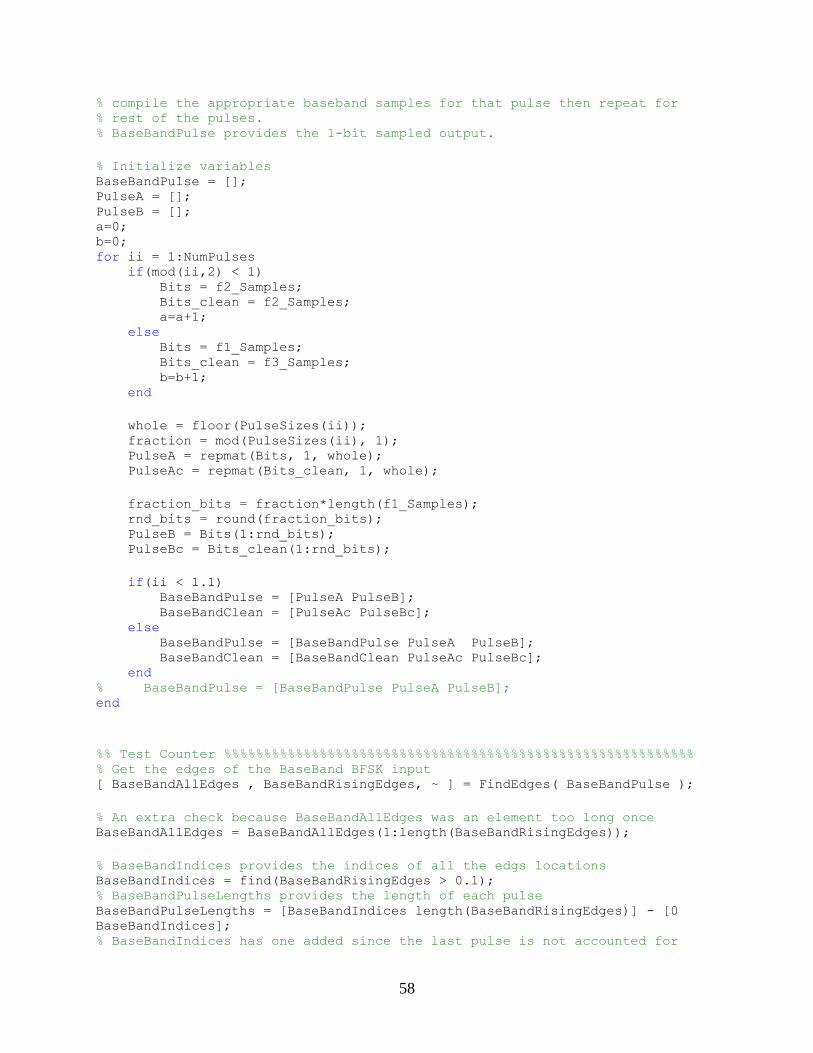
58
% compile the appropriate baseband samples for that pulse then repeat for % rest of the pulses. % BaseBandPulse provides the 1-bit sampled output.
% Initialize variables BaseBandPulse = []; PulseA = []; PulseB = []; a=0; b=0; for ii = 1:NumPulses if(mod(ii,2) < 1) Bits = f2_Samples; Bits_clean = f2_Samples; a=a+1; else Bits = f1_Samples; Bits_clean = f3_Samples; b=b+1; end
whole = floor(PulseSizes(ii)); fraction = mod(PulseSizes(ii), 1); PulseA = repmat(Bits, 1, whole); PulseAc = repmat(Bits_clean, 1, whole);
fraction_bits = fraction*length(f1_Samples); rnd_bits = round(fraction_bits); PulseB = Bits(1:rnd_bits); PulseBc = Bits_clean(1:rnd_bits);
if(ii < 1.1) BaseBandPulse = [PulseA PulseB]; BaseBandClean = [PulseAc PulseBc]; else BaseBandPulse = [BaseBandPulse PulseA PulseB]; BaseBandClean = [BaseBandClean PulseAc PulseBc]; end % BaseBandPulse = [BaseBandPulse PulseA PulseB]; end
%% Test Counter %%%%%%%%%%%%%%%%%%%%%%%%%%%%%%%%%%%%%%%%%%%%%%%%%%%%%%%%%%% % Get the edges of the BaseBand BFSK input [ BaseBandAllEdges , BaseBandRisingEdges, ~ ] = FindEdges( BaseBandPulse );
% An extra check because BaseBandAllEdges was an element too long once BaseBandAllEdges = BaseBandAllEdges(1:length(BaseBandRisingEdges));
% BaseBandIndices provides the indices of all the edgs locations BaseBandIndices = find(BaseBandRisingEdges > 0.1); % BaseBandPulseLengths provides the length of each pulse BaseBandPulseLengths = [BaseBandIndices length(BaseBandRisingEdges)] - [0
BaseBandIndices]; % BaseBandIndices has one added since the last pulse is not accounted for
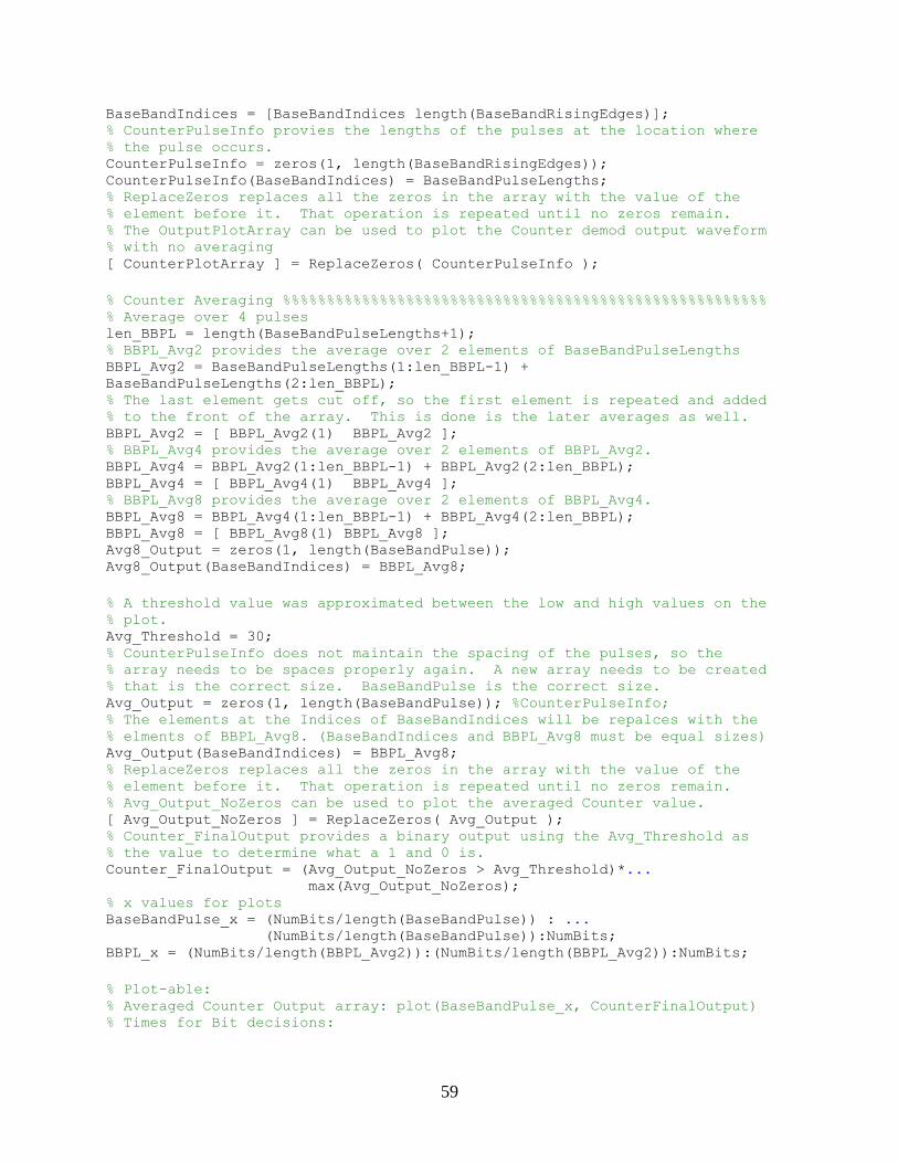
59
BaseBandIndices = [BaseBandIndices length(BaseBandRisingEdges)]; % CounterPulseInfo provies the lengths of the pulses at the location where % the pulse occurs. CounterPulseInfo = zeros(1, length(BaseBandRisingEdges)); CounterPulseInfo(BaseBandIndices) = BaseBandPulseLengths; % ReplaceZeros replaces all the zeros in the array with the value of the % element before it. That operation is repeated until no zeros remain. % The OutputPlotArray can be used to plot the Counter demod output waveform % with no averaging [ CounterPlotArray ] = ReplaceZeros( CounterPulseInfo );
% Counter Averaging %%%%%%%%%%%%%%%%%%%%%%%%%%%%%%%%%%%%%%%%%%%%%%%%%%%%%%% % Average over 4 pulses len_BBPL = length(BaseBandPulseLengths+1); % BBPL_Avg2 provides the average over 2 elements of BaseBandPulseLengths BBPL_Avg2 = BaseBandPulseLengths(1:len_BBPL-1) +
BaseBandPulseLengths(2:len_BBPL); % The last element gets cut off, so the first element is repeated and added % to the front of the array. This is done is the later averages as well. BBPL_Avg2 = [ BBPL_Avg2(1) BBPL_Avg2 ]; % BBPL_Avg4 provides the average over 2 elements of BBPL_Avg2. BBPL_Avg4 = BBPL_Avg2(1:len_BBPL-1) + BBPL_Avg2(2:len_BBPL); BBPL_Avg4 = [ BBPL_Avg4(1) BBPL_Avg4 ]; % BBPL_Avg8 provides the average over 2 elements of BBPL_Avg4. BBPL_Avg8 = BBPL_Avg4(1:len_BBPL-1) + BBPL_Avg4(2:len_BBPL); BBPL_Avg8 = [ BBPL_Avg8(1) BBPL_Avg8 ]; Avg8_Output = zeros(1, length(BaseBandPulse)); Avg8_Output(BaseBandIndices) = BBPL_Avg8;
% A threshold value was approximated between the low and high values on the % plot. Avg_Threshold = 30; % CounterPulseInfo does not maintain the spacing of the pulses, so the % array needs to be spaces properly again. A new array needs to be created % that is the correct size. BaseBandPulse is the correct size. Avg_Output = zeros(1, length(BaseBandPulse)); %CounterPulseInfo; % The elements at the Indices of BaseBandIndices will be repalces with the % elments of BBPL_Avg8. (BaseBandIndices and BBPL_Avg8 must be equal sizes) Avg_Output(BaseBandIndices) = BBPL_Avg8; % ReplaceZeros replaces all the zeros in the array with the value of the % element before it. That operation is repeated until no zeros remain. % Avg_Output_NoZeros can be used to plot the averaged Counter value. [ Avg_Output_NoZeros ] = ReplaceZeros( Avg_Output ); % Counter_FinalOutput provides a binary output using the Avg_Threshold as % the value to determine what a 1 and 0 is. Counter_FinalOutput = (Avg_Output_NoZeros > Avg_Threshold)*... max(Avg_Output_NoZeros); % x values for plots BaseBandPulse_x = (NumBits/length(BaseBandPulse)) : ... (NumBits/length(BaseBandPulse)):NumBits; BBPL_x = (NumBits/length(BBPL_Avg2)):(NumBits/length(BBPL_Avg2)):NumBits;
% Plot-able: % Averaged Counter Output array: plot(BaseBandPulse_x, CounterFinalOutput) % Times for Bit decisions:
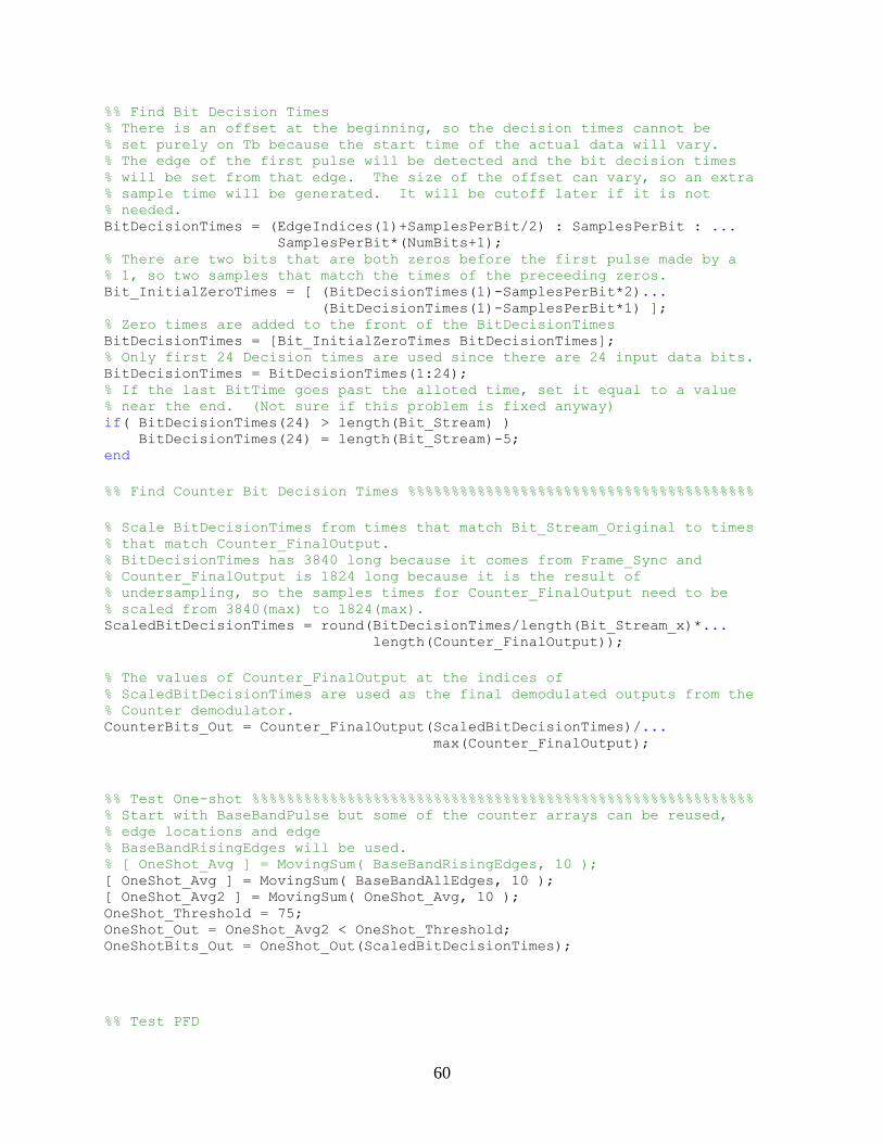
60
%% Find Bit Decision Times % There is an offset at the beginning, so the decision times cannot be % set purely on Tb because the start time of the actual data will vary. % The edge of the first pulse will be detected and the bit decision times % will be set from that edge. The size of the offset can vary, so an extra % sample time will be generated. It will be cutoff later if it is not % needed. BitDecisionTimes = (EdgeIndices(1)+SamplesPerBit/2) : SamplesPerBit : ... SamplesPerBit*(NumBits+1); % There are two bits that are both zeros before the first pulse made by a % 1, so two samples that match the times of the preceeding zeros. Bit_InitialZeroTimes = [ (BitDecisionTimes(1)-SamplesPerBit*2)... (BitDecisionTimes(1)-SamplesPerBit*1) ]; % Zero times are added to the front of the BitDecisionTimes BitDecisionTimes = [Bit_InitialZeroTimes BitDecisionTimes]; % Only first 24 Decision times are used since there are 24 input data bits. BitDecisionTimes = BitDecisionTimes(1:24); % If the last BitTime goes past the alloted time, set it equal to a value % near the end. (Not sure if this problem is fixed anyway) if( BitDecisionTimes(24) > length(Bit_Stream) ) BitDecisionTimes(24) = length(Bit_Stream)-5; end
%% Find Counter Bit Decision Times %%%%%%%%%%%%%%%%%%%%%%%%%%%%%%%%%%%%%%%%
% Scale BitDecisionTimes from times that match Bit_Stream_Original to times % that match Counter_FinalOutput. % BitDecisionTimes has 3840 long because it comes from Frame_Sync and % Counter_FinalOutput is 1824 long because it is the result of % undersampling, so the samples times for Counter_FinalOutput need to be % scaled from 3840(max) to 1824(max). ScaledBitDecisionTimes = round(BitDecisionTimes/length(Bit_Stream_x)*... length(Counter_FinalOutput));
% The values of Counter_FinalOutput at the indices of % ScaledBitDecisionTimes are used as the final demodulated outputs from the % Counter demodulator. CounterBits_Out = Counter_FinalOutput(ScaledBitDecisionTimes)/... max(Counter_FinalOutput);
%% Test One-shot %%%%%%%%%%%%%%%%%%%%%%%%%%%%%%%%%%%%%%%%%%%%%%%%%%%%%%%%%% % Start with BaseBandPulse but some of the counter arrays can be reused, % edge locations and edge % BaseBandRisingEdges will be used. % [ OneShot_Avg ] = MovingSum( BaseBandRisingEdges, 10 ); [ OneShot_Avg ] = MovingSum( BaseBandAllEdges, 10 ); [ OneShot_Avg2 ] = MovingSum( OneShot_Avg, 10 ); OneShot_Threshold = 75; OneShot_Out = OneShot_Avg2 < OneShot_Threshold; OneShotBits_Out = OneShot_Out(ScaledBitDecisionTimes);
%% Test PFD
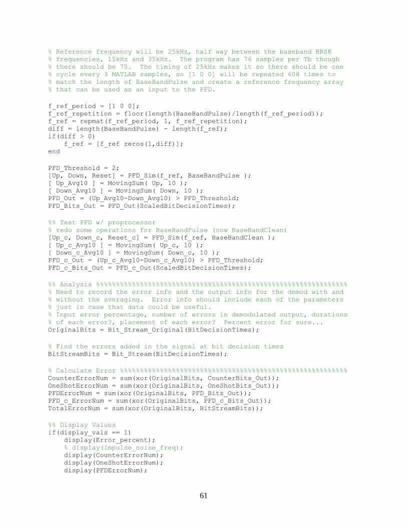
61
% Reference frequency will be 25kHz, half way between the baseband BRSK % frequencies, 15kHz and 35kHz. The program has 76 samples per Tb though % there should be 75. The timing of 25kHz makes it so there should be one % cycle every 3 MATLAB samples, so [1 0 0] will be repeated 608 times to % match the length of BaseBandPulse and create a reference frequency array % that can be used as an input to the PFD.
f_ref_period = [1 0 0]; f_ref_repetition = floor(length(BaseBandPulse)/length(f_ref_period)); f_ref = repmat(f_ref_period, 1, f_ref_repetition); diff = length(BaseBandPulse) - length(f_ref); if(diff > 0) f_ref = [f_ref zeros(1,diff)]; end
PFD_Threshold = 2; [Up, Down, Reset] = PFD_Sim(f_ref, BaseBandPulse ); [ Up_Avg10 ] = MovingSum( Up, 10 ); [ Down_Avg10 ] = MovingSum( Down, 10 ); PFD_Out = (Up_Avg10-Down_Avg10) > PFD_Threshold; PFD_Bits_Out = PFD_Out(ScaledBitDecisionTimes);
%% Test PFD w/ proprocessor % redo some operations for BaseBandPulse (now BaseBandClean) [Up_c, Down_c, Reset_c] = PFD_Sim(f_ref, BaseBandClean ); [ Up_c_Avg10 ] = MovingSum( Up_c, 10 ); [ Down_c_Avg10 ] = MovingSum( Down_c, 10 ); PFD_c_Out = (Up_c_Avg10-Down_c_Avg10) > PFD_Threshold; PFD_c_Bits_Out = PFD_c_Out(ScaledBitDecisionTimes);
%% Analysis %%%%%%%%%%%%%%%%%%%%%%%%%%%%%%%%%%%%%%%%%%%%%%%%%%%%%%%%%%%%%%% % Need to record the error info and the output info for the demod with and % without the averaging. Error info should include each of the parameters % just in case that data could be useful. % Input error percentage, number of errors in demodulated output, durations % of each error?, placement of each error? Percent error for sure... OriginalBits = Bit_Stream_Original(BitDecisionTimes);
% Find the errors added in the signal at bit decision times BitStreamBits = Bit_Stream(BitDecisionTimes);
% Calculate Error %%%%%%%%%%%%%%%%%%%%%%%%%%%%%%%%%%%%%%%%%%%%%%%%%%%%%%%%% CounterErrorNum = sum(xor(OriginalBits, CounterBits_Out)); OneShotErrorNum = sum(xor(OriginalBits, OneShotBits_Out)); PFDErrorNum = sum(xor(OriginalBits, PFD_Bits_Out)); PFD_c_ErrorNum = sum(xor(OriginalBits, PFD_c_Bits_Out)); TotalErrorNum = sum(xor(OriginalBits, BitStreamBits));
%% Display Values if(display_vals == 1) display(Error_percent); % display(Impulse_noise_freq); display(CounterErrorNum); display(OneShotErrorNum); display(PFDErrorNum);
62
display(PFD_c_ErrorNum); display(TotalErrorNum);
end
%% Save Variables %%%%%%%%%%%%%%%%%%%%%%%%%%%%%%%%%%%%%%%%%%%%%%%%%%%%%%%%% % FileName = 'D:\Google Drive\1A_Thesis\MATLAB_Files\DemodErrorData_2.mat'; ErrorPercentAll = [ErrorPercentAll Error_percent ]; CounterErrorNumAll = [CounterErrorNumAll CounterErrorNum ]; OneShotErrorNumAll = [OneShotErrorNumAll OneShotErrorNum ]; PFDErrorNumAll = [PFDErrorNumAll PFDErrorNum ]; PFD_c_ErrorNumAll = [PFD_c_ErrorNumAll PFD_c_ErrorNum ]; TotalErrorNumAll = [TotalErrorNumAll TotalErrorNum ];
save(FileName, 'ErrorPercentAll', 'TotalErrorNumAll',
'CounterErrorNumAll',... 'OneShotErrorNumAll', 'PFDErrorNumAll', 'PFD_c_ErrorNumAll' );
%% Plots %% Use the stair function for any plots in the paper **********************
if(plot_error == 1) % plot error stream, bit stream, and bit stream with errors figure(1); clf; hold on; plot(Bit_Stream_x, Bit_Stream, 'b'); plot(Bit_Stream_x, Bit_Stream_Original+1.1, 'r'); plot(Bit_Stream_x, error_stream + 2.2); plot_len1 = length(Bit_Stream); plot(BitDecisionTimes/length(Bit_Stream_x)*24, ... ones(1, length(BitDecisionTimes)), 'rx'); axis([0 NumBits -0.1 3.3]);
% plot baseband BFSK figure(3); clf; hold on; plot(BaseBandPulse_x, BaseBandPulse + 1.1, 'b'); plot(Bit_Stream_x, Bit_Stream, 'b') plot_len3 = length(BaseBandPulse); axis([0 NumBits -0.1 2.2]);
% plot Counter figure(4); clf; hold on;
subplot(5,1,1); hold on; plot(BBPL_x, BaseBandPulseLengths); axis([0 NumBits -0.1 max(BaseBandPulseLengths+1)]);
subplot(5,1,2); hold on plot(BBPL_x, BBPL_Avg2); axis([0 NumBits -0.1 max(BBPL_Avg2+1)]);
subplot(5,1,3); hold on plot(BBPL_x, BBPL_Avg4); axis([0 NumBits -0.1 max(BBPL_Avg4+1)]);
subplot(5,1,4); hold on
63
plot(BaseBandPulse_x, Avg8_Output); axis([0 NumBits -0.1 max(BBPL_Avg8+1)]);
subplot(5,1,5); hold on plot(BaseBandPulse_x, Avg_Output); plot(BaseBandPulse_x, Avg_Output_NoZeros, 'g--'); plot(BaseBandPulse_x, Counter_FinalOutput, 'r'); plot(BitDecisionTimes/length(Bit_Stream_x)*24, ... ones(1, length(BitDecisionTimes))*max(Counter_FinalOutput), 'ro'); axis([0 NumBits -0.1 max(Avg_Output+2.1)]);
% plot Counter Outline figure(6); clf; hold on; plot(BaseBandPulse_x, CounterPulseInfo, 'b'); plot(BaseBandPulse_x, CounterPlotArray, 'r'); plot(BitDecisionTimes/length(Bit_Stream_x)*24,... ones(1, length(BitDecisionTimes))*max(CounterPlotArray), 'gx'); axis([0 NumBits -0.1 (max(CounterPlotArray) + 1)]);
% plot One-Shot figure(7); clf; hold on; subplot(2,1,1); plot(BaseBandPulse_x, OneShot_Avg2, 'b'); axis([0 NumBits (min(OneShot_Avg2) - 1) (max(OneShot_Avg2) + 1)]); subplot(2,1,2); hold on; plot(BaseBandPulse_x, OneShot_Out, 'b'); plot(BitDecisionTimes/length(Bit_Stream_x)*24,... ones(1, length(BitDecisionTimes)), 'gx'); % plot(OneShotBits_Out axis([0 NumBits -0.1 1.1]);
% plot PFD figure(8); clf; hold on; subplot(3,1,1); hold on; plot(BaseBandPulse_x, Up_Avg10 + (max(Down_Avg10)+1.1)); plot(BaseBandPulse_x, Down_Avg10); axis([0 NumBits -0.1 2*(max(Down_Avg10)+1.1)]); subplot(3,1,2); hold on; plot(BaseBandPulse_x, Up_Avg10-Down_Avg10); axis([0 NumBits -1*(max(Down_Avg10)+1.1) (max(Down_Avg10)+1.1)]); subplot(3,1,3); hold on; plot(BaseBandPulse_x, PFD_Out, 'b'); plot(BitDecisionTimes/length(Bit_Stream_x)*24,... ones(1, length(BitDecisionTimes)), 'gx'); axis([0 NumBits -0.1 1.1]);
% plot PFD w/preprocessing figure(9); clf; hold on; plot(BaseBandPulse_x, BaseBandPulse + 2.2, 'b'); plot(BaseBandPulse_x, BaseBandClean + 1.1, 'b'); plot(Bit_Stream_x, Bit_Stream, 'b') plot_len3 = length(BaseBandPulse); axis([0 NumBits -0.1 3.3]);
figure(10); clf; hold on; subplot(3,1,1); hold on;
64
plot(BaseBandPulse_x, Up_c_Avg10 + (max(Down_c_Avg10)+1.1)); plot(BaseBandPulse_x, Down_c_Avg10); axis([0 NumBits -0.1 2*(max(Down_c_Avg10)+1.1)]); subplot(3,1,2); hold on; plot(BaseBandPulse_x, Up_c_Avg10-Down_c_Avg10); axis([0 NumBits -1*(max(Down_c_Avg10)+1.1) (max(Down_c_Avg10)+1.1)]); subplot(3,1,3); hold on; plot(BaseBandPulse_x, PFD_c_Out, 'b'); plot(BitDecisionTimes/length(Bit_Stream_x)*24,... ones(1, length(BitDecisionTimes)), 'gx'); axis([0 NumBits -0.1 1.1]);
end
% End Function
End
Supporting Modules
Error Generation
function [ Error_percent, Impulse_noise_freq , error_stream, Bit_Stream,
Bit_Stream_Original ] = Frame_Sync_Sim_BitInput( )
%Charles Carlson %System to simulate Correlation Frame Sync Performance %Oct 7th 2014 %Updated on October 28th, to have impulse noise only effect SW % clear all % % ** This version of the code was adapted to fit the needs for Riley % Harrington's FSK demodulator error testing. **
% Comments were added and some unneeded code was removed by Harrington
% for this version. %%%%%%%%%%%%%%%%%%%%%%%%%%%%%%%%%%%%%%%%%%%%%%%%%%%%%%%%%% %System Parameters Oversampling_ratio = 16; % 16 Samples per bit DataRate = 20000; % Datarate = 20k BitTime = 1/DataRate; % BitTime = 50us SamplingRate = Oversampling_ratio*DataRate; % fs = 320k SampleTime = 1/SamplingRate; % Ts = 3.125us TotalBits = 24; % 24 Bits in each frame sent TotalTime = (TotalBits*BitTime); % 24*50us = 1.2ms DataPoints = TotalTime/SampleTime; % 1.2ms/3.125us = 384 SNR_dB = 0; % Only variable use is commented out Resolution = 10; % number of Matlab points per sample % Number of MATLAB samples per bit = Oversampling_ratio*Resolution = 160 % Min lenght of an "error" is the size of Resolution, 10. Max_Impulses = 5; % max number of noise impulses %%%%%%%%%%%%%%%%%%%%%%%%%%%%%%%%%%%%%%%%%%%%%%%%%%%%%%%%%%%%%%%%%%%%%% %Number of simulations run = 1; % Number of runs per simulation
65
Sync_array = zeros(1,run); % Used to record if noisy data synced correctly False_Sync_array = zeros(1,run); % Used to record if data synced when it
shouldn't have
%% For Loop executes code to simulate each "run" for run_index = 1:run Synchronization = 0; %Indicates if received frame has synced False_sync = 0; %Indicates if frame synched at incorrect time
%Need Bit Stream to start at random time, can range from 0 to Bit_Time %Finds random time to to start bit stream, so stream will not %necessarily start at the beginning of the simulated bit time. BitTime %is 50us, so the stream will start between 0us and 50us data_start = rand(1)*BitTime; %The start time needs to be coerced to the nearest resolution %available. For initial to get set properly, the start time %(data_start) would need to be divided by the SampleTime. %To account for resolution, the result needs to be muliplied by the %resolution (10). initial = round(data_start/SampleTime * Resolution); %Matlab is 1 indexed and the line above has the possibility of being a %zero, so increase value by one initial = initial+1;
%Setup time and data vectors %Initialize vector to fit size of Matlab bits needed Bit_Stream = zeros(1,Resolution*DataPoints); i = 1; k = 1; % generate random vector that will be used for testing on this run r_v = round(rand(1,8)); %8 zero bits added on front
%% Frame Options
% Demods will be tested with Ethernet frame, so others frames were % removed (saved at bottom of file) % demods could just use a totally random vector as long as the input % and output are known and compared.
%Ethernet 10101011 % Changing 8th bit to always be the same as 7th bit. % With the shifting that happens, the 8th bit can be too narrow to % effectivly detect which throws off the error check. r_v(8) = r_v(7);
Frame_bits = [0 0 1 0 1 0 0 0 1 0 1 0 1 0 1 1 r_v(1) r_v(2) r_v(3)... r_v(4) r_v(5) r_v(6) r_v(7) r_v(8)];
Initial_Frame_bits = Frame_bits; %Initial_Frame_bits = [0 0 0 0 0 0 0 0 0 1 0 1 0 1 1 1 0 0 0 0 0 0 0 0];
%used for correlation %random_bits = round(rand(1,TotalBits-16));
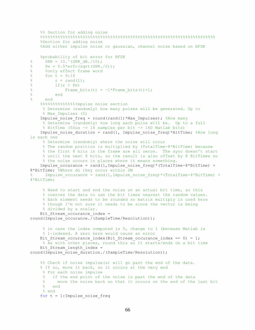
66
%% Section for adding noise %%%%%%%%%%%%%%%%%%%%%%%%%%%%%%%%%%%%%%%%%%%%%%%%%%%%%%%%%%%%%%%%%%%%%% %Section for adding noise %Add either impulse noise or gaussian, channel noise based on BFSK
%probability of bit error for BFSK % SNR = 10.^(SNR_dB./10); % Pe = 0.5*erfc(sqrt(SNR./2)); % %only effect frame word % for t = 9:16 % r = rand(1); % if(r < Pe) % Frame_bits(t) = -1*Frame_bits(t)+1; % end % end %%%%%%%%%%%%%%Impulse noise section % Determine (randomly) how many pulses will be generated. Up to % Max_Impulses (5) Impulse_noise_freq = round(rand(1)*Max_Impulses); %How many % Determine (randomly) how long each pulse will be. Up to a full % BitTime (50us -> 16 samples per bit -> 160 Matlab bits) Impulse_noise_duration = rand(1, Impulse_noise_freq)*BitTime; %How long
is each one % Determine (randomly) where the noise will occur % The random position is multiplied by (TotalTime-8*BitTime) because % the first 8 bits in the frame are all zeros. The sync doesn't start % until the next 8 bits, so the result is also offset by 8 BitTimes so % the noise occurs in places where it means something. Impulse_occurance = rand(1,Impulse_noise_freq)*(TotalTime-8*BitTime) +
8*BitTime; %Where do they occur within SW % Impulse_occurance = rand(1,Impulse_noise_freq)*(TotalTime-4*BitTime) +
4*BitTime;
% Need to start and end the noise on an actual bit time, so this % coerces the data to use the bit times nearest the random values. % Each element needs to be rounded so matrix multiply is used here % though I'm not sure it needs to be since the vector is being % divided by a scalar. Bit_Stream_occurance_index =
round(Impulse_occurance./(SampleTime/Resolution));
% in case the index computed is 0, change to 1 (because Matlab is % 1-indexed. A zero here would cause an error Bit_Stream_occurance_index(Bit_Stream_occurance_index == 0) = 1; % As with other places, round this so it starts/ends on a bit time Bit_Stream_length_index =
round(Impulse_noise_duration./(SampleTime/Resolution));
%% Check if noise impulse(s) will go past the end of the data. % If so, move it back, so it occurs at the very end % For each noise impulse % if the end point of the noise is past the end of the data % move the noise back so that it occurs on the end of the last bit % end % end for t = 1:Impulse_noise_freq
67
if(Bit_Stream_occurance_index(t)+Bit_Stream_length_index(t) >
Resolution*DataPoints) Bit_Stream_length_index(t) = Resolution*DataPoints -
Bit_Stream_occurance_index(t); end end
%% %%%%%%%%%%%%%%%%%%%%%%%%%%%%%%%%%%%%%%%%%%%%%%%%%%%%%%%%%%%%%%%%%%%%%% % Stop variables are used to find the stop bits in the sync frame % ^ I think?? stop1 = 0; stop2 = 0;
%Setup Bit Stream % data start is close to starting at zero, so the end needs to happen % at Time minus 1 % some of this could likely be done without loops for Time_array = data_start:(SampleTime/Resolution):(TotalTime-
SampleTime/Resolution) % if the array isn't past all the sync bits and into the actual % data, set Bit_Stream to the initial bit (zero). if(Time_array < (BitTime+data_start)) Bit_Stream(initial+i) = Frame_bits(1); end
% Does this run for the last bit? for k = 1:TotalBits-1 if(k < 24) % 24 could be replaced w/TotalBits variable? % There are only 24 frame bits and that's hard coded, so I % don't know what this does? if(Time_array >= k*BitTime+data_start) Bit_Stream(initial+i) = Frame_bits(k+1); end end end %%%%%%%%%%%%%%%%%%%%%%%%%%%%%%%%%%%%%%%%%%%%%%%%%%%%% %for testing results if(Time_array >= 15*BitTime+data_start && stop1 == 0) Correct_sync_start = (initial+i); stop1 = 1; end if(Time_array >= 16*BitTime+data_start && stop2 == 0) Correct_sync_stop = (initial+i); stop2 = 1; end %%%%%%%%%%%%%%%%%%%%%%%%%%%%%%%%%%%%%%%%%%%%%%%%%%%%% i = i + 1; end Bit_Stream = Bit_Stream(1:Resolution*DataPoints); Time_array = 0:(SampleTime/Resolution):(TotalTime-
(SampleTime/Resolution)); %%%%%%%%%%%%%%%%%%%%%%%%%%%%%%%%%%%%%%%%%%%%%%%%%%%%%%%%%%%%%%%%%%%%%% %Add impulse noise % adding a variable to save wavefrom w/o impulse noise Bit_Stream_Original = Bit_Stream;
68
for t = 1:Impulse_noise_freq
Bit_Stream(Bit_Stream_occurance_index(t):Bit_Stream_occurance_index(t)+Bit_St
ream_length_index(t)) =... -
1*Bit_Stream(Bit_Stream_occurance_index(t):Bit_Stream_occurance_index(t)+Bit_
Stream_length_index(t))+1; end
% Sometimes the last bit in the array would be different for no good % reason, so this will set the last bit equal to the 2nd to last bit Bit_Stream_Original(length(Bit_Stream_Original)-1) =
Bit_Stream_Original(length(Bit_Stream_Original)-1); Bit_Stream(length(Bit_Stream_Original)) =
Bit_Stream(length(Bit_Stream_Original)-1);
end Failed_Sync_count = sum(Sync_array(1,:) == 0); False_Sync_count = sum(False_Sync_array);
%% Changed code %Changed line below to line above, so it made more sense to me %initial = round(data_start/(SampleTime/Resolution)); %%
error_stream = xor(Bit_Stream, Bit_Stream_Original); %display(Impulse_noise_freq); % Multiply by 2/3 because the error only occurs on the last 16 bits, and % never on the first 8 bits. Error_percent = sum(error_stream)/length(error_stream)*(2/3);
end
Find Edges
function [ AllEdges, Rising, Falling ] = FindEdges( Waveform ) %% FindEdges Summary of this function goes here
% Find Edges Full = [Waveform 0] - [0 Waveform]; % Find Rising Edges Rising = Full(1:(length(Full)-1)) > 0; % Find Falling Edges Falling = Full(1:(length(Full)-1)) < 0;
%AllEdges = AllEdges(1:length(AllEdges)-1); AllEdges = Rising | Falling;
end
69
Subsampling
function [ Samples_out, W, R ] = UnderSample( f_in, f_s ) %% % Riley Harrington % Kansas State University
% If the input is constant for a period of time and the first sample is % acquired to give the first value (initial condition?), then the rest of % the sample values should be easy to simulate
%% Test Values; Comment out when using file as function % f_s = 75e3; %75kHz % Sample Frequency % f_in = 10.71e6; % Input Frequency
T_s = 1/f_s; % Sample Period T_in = 1/f_in; % Input Period DataPeriod = 1e-3; %0.1ms
%% Pattern Info W = floor(f_in/f_s); R = mod((f_in/f_s), 1);
SampleTimes = 0:T_s:DataPeriod; Samples = R:R:(length(SampleTimes)*R); Samples_R = mod(Samples, 1); IntStep1 = Samples_R>0.999; Samples_R_OnesRemoved = abs(Samples_R - IntStep1); Samples_R_OnesRemoved_Rounded = round(Samples_R_OnesRemoved); Samples_out = Samples_R_OnesRemoved_Rounded;
Replace Zeros
function [ OutputArray ] = ReplaceZeros( InputArray ) %% % Riley Harrington % Kansas State University %%
% InputArray = [1 0 0 0 0 0 0 0 5 0 0 0 1 2 0 0 0 7 0 3 3 3 0 0 1 0 0]; IntArray = InputArray;
ArrayZerosIndices = find(IntArray < 0.1); ArrayZerosRemaining = length(ArrayZerosIndices);
while(ArrayZerosRemaining > 0) IntArray(ArrayZerosIndices) = IntArray(ArrayZerosIndices - 1);
% Update Loop Index ArrayZerosIndices = find(IntArray < 0.1); ArrayZerosRemaining = length(ArrayZerosIndices);
70
end
OutputArray = IntArray;
end
Repeat Elements
function [ NewArray ] = RepeatElements( Array, N ) %% % Riley Harrington % Kansas State University %%
% Test Inputs % Array = [1 2 3 4 5]; % N = 4; % to repear whole array, used b = repmat(Array, 1, N);
b = repmat(Array, N, 1); NewArray = reshape(b, 1, length(Array)*N); end
Averaging Filter
function [ OutputArray ] = MovingSum( InputArray, N ) %% % Riley Harrington % Kansas State University %% % Function description %%
%% Test Inputs % InputArray = [1 1 0 0 1 0 1 0 1 3 1 0 ]; % N = 4; %%
TempArray = InputArray; for ii = 1:N [TempArray] = MoveSum(InputArray, TempArray, ii);
end % [OutputArray] = MoveSum(InputArray); OutputArray = TempArray;
end
function [OutputArray] = MoveSum(InputArray, TempArray, N)
% Check Array length
71
if(length(InputArray) <= N) OutputArray = []; else NewArray = InputArray( 1 : length(InputArray) - N ) + ... TempArray( (1+N) : length(TempArray) ); % Add the first element to the front, so the Input and Output arrays % have the same length. OutputArray = [NewArray(1:N) NewArray]; end end