formation of oxide films for high-capacitance aluminum ... · formation of oxide films for...
TRANSCRIPT
Instructions for use
Title Formation of oxide films for high-capacitance aluminum electrolytic capacitor by liquid-phase deposition and anodizing
Author(s) Sakairi, Masatoshi; Fujita, Ryota; Nagata, Shinji
Citation Surface and Interface Analysis, 48(8): 899-905
Issue Date 2016-08
Doc URL http://hdl.handle.net/2115/66901
RightsThis is the peer reviewed version of the following article: Surface and interface analysis, 48(8), August 2016, pp.899-905, which has been published in final form athttp://onlinelibrary.wiley.com/doi/10.1002/sia.5851/full. This article may be used for non-commercial purposes inaccordance with Wiley Terms and Conditions for Self-Archiving.
Type article (author version)
File Information Sakair-SIA48(8)899-905.pdf
Hokkaido University Collection of Scholarly and Academic Papers : HUSCAP
Formation of oxide films for high-capacitance aluminum electrolytic capacitor by liquid phase deposition and anodizing Masatoshi. Sakairi1), Ryota Fujita2), and Shinji Nagata3)
1)Faculty of Engineering, Hokkaido University, Kita-13, Nishi-8, Kita-ku, Sapporo, 060-8628, Japan 2)Graduate School of Engineering, Hokkaido University, Kita-13, Nishi-8, Kita-ku, Sapporo, 060-8628, Japan (Presently; Frukawa Electric CO. LTD., 601-2, Otorizawa, Nikko, 321-2336, Japan) 3) Institute for Materials Research, Tohoku University, Katahira-2-1-1, Aoba-ku, Sendai, 980-8577, Japan
Abstract Liquid phase deposition (LPD) treatment and anodizing were used to form oxide layer for a high-capacitance aluminum electrolytic capacitor. Formation of protective oxide layers and modification of LPD conditions make it possible to prolong the LPD duration and lead to the formation of TiO2 and NaF deposits on aluminum. A titanium oxide / aluminum oxide mixed layer was formed by a combination process of LPD treatment and anodizing. The capacitance of the formed layer was about 300% higher than that of an anodic oxide film formed on electropolished aluminum. The structures and compositions of the films that were formed were determined by transmission electron microscopy, scanning electron microscopy, and Rutherford backscattering spectroscopy. Keywords: dielectric film, liquid phase deposition, anodizing, aluminum, titanium oxide.
Introduction Capacitors such as an aluminum electrolytic capacitor are indispensable components in electrical equipment. Due to the demand for reduction in size and weight of electronic devices, small and high-capacitance capacitors have been required. One of the authors studied incorporation of silicon, niobium or zirconium oxides into anodic oxide films on aluminum to increase specific dielectric constants[1-9]. The electric capacitance achieved was less than 200% of that of an anodic oxide film formed on aluminum without coating. Sol-gel or metal-oxide chemical vapor deposition techniques were used in previous studies for formation of thin oxide films. These techniques have been used for the formation of thin and compact oxide layers on materials. However, the chemicals used in these techniques are costly and require dry conditions during storage and film formation processes. Therefore, a simple technique for the formation of form oxide layers is needed. One simpler technique is liquid phase deposition (LPD) treatment. LPD treatment is a new surface coating technique for the formation of metal oxide films by dipping the substrate in an aqueous solution[10]. This technique can be used for the formation of metal oxide films on many kinds of substrates. Deki et al. reported fabrication of TiO2 nanostructures with diameters ranging from 120 to 1065 nm on Si wafers with LPD and electron lithography[11]. Huang et al. reported formation of a self-cleaning and antireflection TiO2 film on silicon for silicon-based solar cells[12]. The formed film had low water contact angle around 4˚ and the average reflectance of TiO2/Si structure was 5.3%. Mizuhata et al. reported that formation of TiO2/porous Si nonocomposites for lithium ion battery by LPD with anodizing[13, 14]. The formed TiO2/porous Si showed high charge/discharge capacity without rapid degradation. Wu et at. reported formation of an SrTiO3 film on an AlGN/GaN wafer for gate dielectric in a metal oxide semiconductor high electron mobility transistor (MOSHEMT)[15]. Lei et al. reported a dense and crack-free anatase TiO2 film with thickness of 800 nm was formed by LPD at 353K for 10.8 ks on ITO conducting grass as photo-anodes for cathodic protection of SUS 304 stainless steel[16]. Lee et al. reported fabrication of photocatalytic TiO2 films on stainless steel by LPD at 333 K using TiF4 and H3BO3
[17]. The formed TiO2 films showed a preferential orientation, and formed films showed photocatalytic activity without high-temperature treatment. The formed TiO2 films exhibited sufficiently negative potential under illumination, and they could serve as the photo anodes for cathodic protection of the steels. Fujita et al. reported formation of corrosion-resistant TiO2 films on magnesium and the structures and chemical compositions of the films[18,
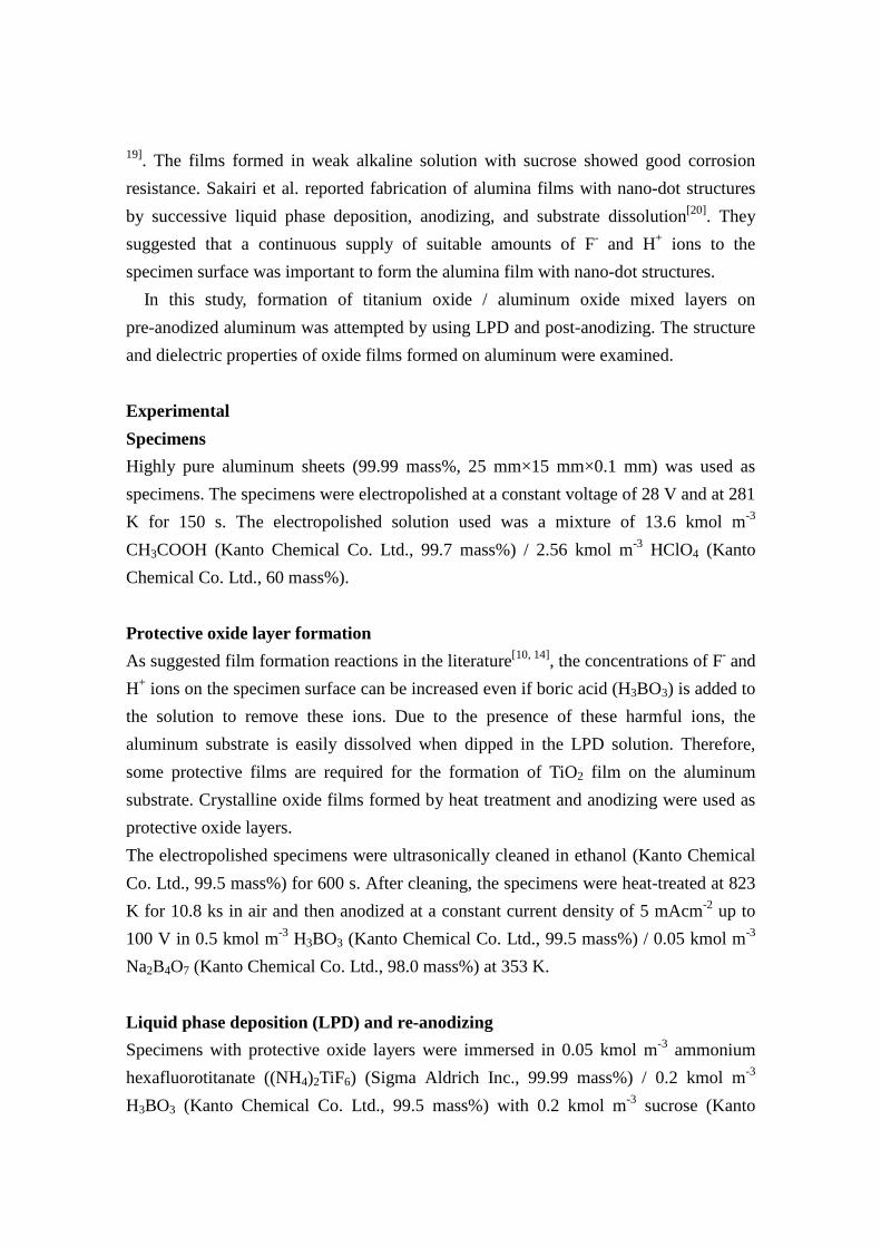
19]. The films formed in weak alkaline solution with sucrose showed good corrosion resistance. Sakairi et al. reported fabrication of alumina films with nano-dot structures by successive liquid phase deposition, anodizing, and substrate dissolution[20]. They suggested that a continuous supply of suitable amounts of F- and H+ ions to the specimen surface was important to form the alumina film with nano-dot structures. In this study, formation of titanium oxide / aluminum oxide mixed layers on pre-anodized aluminum was attempted by using LPD and post-anodizing. The structure and dielectric properties of oxide films formed on aluminum were examined. Experimental Specimens Highly pure aluminum sheets (99.99 mass%, 25 mm×15 mm×0.1 mm) was used as specimens. The specimens were electropolished at a constant voltage of 28 V and at 281 K for 150 s. The electropolished solution used was a mixture of 13.6 kmol m-3 CH3COOH (Kanto Chemical Co. Ltd., 99.7 mass%) / 2.56 kmol m-3 HClO4 (Kanto Chemical Co. Ltd., 60 mass%). Protective oxide layer formation As suggested film formation reactions in the literature[10, 14], the concentrations of F- and H+ ions on the specimen surface can be increased even if boric acid (H3BO3) is added to the solution to remove these ions. Due to the presence of these harmful ions, the aluminum substrate is easily dissolved when dipped in the LPD solution. Therefore, some protective films are required for the formation of TiO2 film on the aluminum substrate. Crystalline oxide films formed by heat treatment and anodizing were used as protective oxide layers. The electropolished specimens were ultrasonically cleaned in ethanol (Kanto Chemical Co. Ltd., 99.5 mass%) for 600 s. After cleaning, the specimens were heat-treated at 823 K for 10.8 ks in air and then anodized at a constant current density of 5 mAcm-2 up to 100 V in 0.5 kmol m-3 H3BO3 (Kanto Chemical Co. Ltd., 99.5 mass%) / 0.05 kmol m-3 Na2B4O7 (Kanto Chemical Co. Ltd., 98.0 mass%) at 353 K. Liquid phase deposition (LPD) and re-anodizing Specimens with protective oxide layers were immersed in 0.05 kmol m-3 ammonium hexafluorotitanate ((NH4)2TiF6) (Sigma Aldrich Inc., 99.99 mass%) / 0.2 kmol m-3 H3BO3 (Kanto Chemical Co. Ltd., 99.5 mass%) with 0.2 kmol m-3 sucrose (Kanto
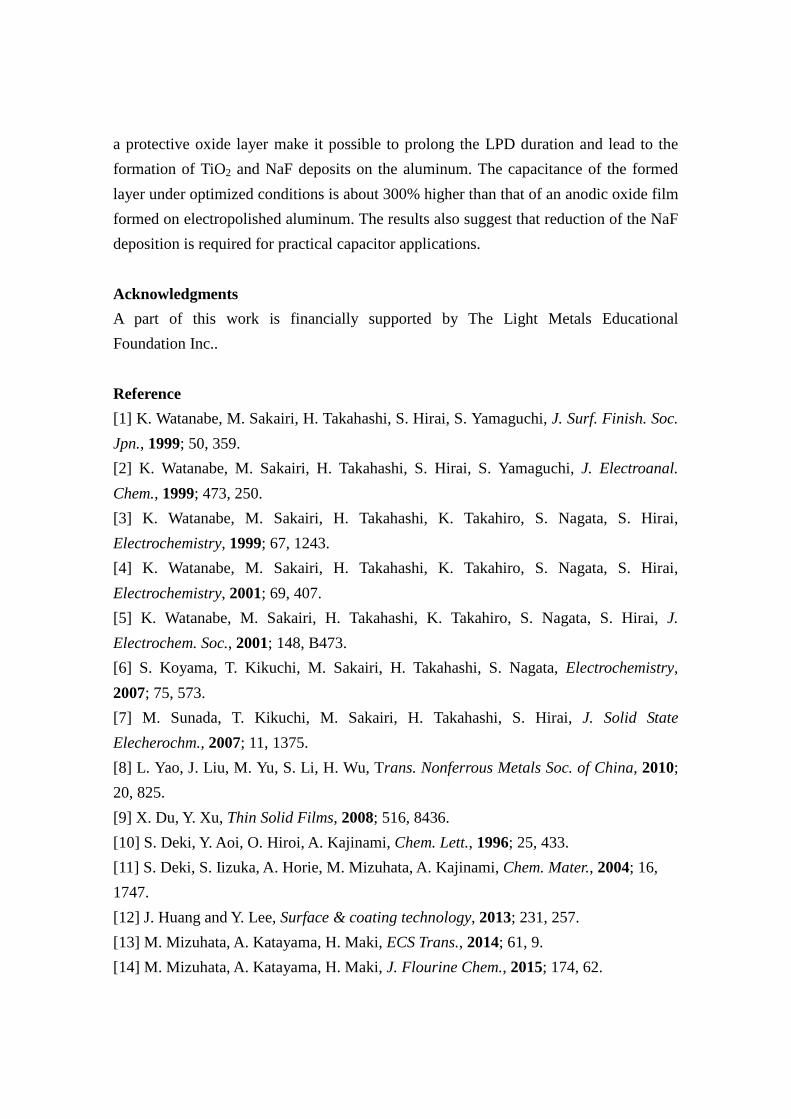
Chemical Co. Ltd., guaranteed reagent) from tL = 0.9 ks to 7.2 ks at 353 K. The pH of the solutions was adjusted with sodium hydroxide (NaOH) (Kanto Chemical Co. Ltd., 97.0 mass%). Sucrose acts an inhibitor for TiO2 excess homogeneous nucleation in LPD solutions. LPD-treated specimens were re-anodized at a constant current density of 1 mAcm-2 up to 100 V in 0.5 kmol m-3 H3BO3 / 0.05 kmol m-3 Na2B4O7 at 293 K. Characterization of the formed films Electrochemical impedance were measured by using a frequency response analyzer (FRA, NF Corporation, S-5720B ) and a sine wave of 100 mV was used. Specimen surfaces after treatment were examined by using a scanning electron microscope (SEM, JEOL Ltd., JSM-6510LA) equipped with an energy dispersive X-ray spectroscope (EDS). Cross sections of the LPD specimens were examined by using a transmission electron microscope (TEM, JEOL Ltd., JEM-2000FX) equipped with an EDS. The oxide films were also analyzed by Rutherford backscattering spectroscopy (RBS, High Voltage Engineering Tandetron) using a 2.0 MeV He2+ ion beam supplied by a Van de Graff accelerator. The He2+ ion beam angle was normal to the specimen surface, and the detector angle was 170 degrees to the incident direction. The chemical compositions and thicknesses of the films that were formed were determined using the RUMP program. Results and discussion Re-anodizing behavior of LPD-treated specimens Figure 1 shows changes in cell voltage, Era, during re-anodizing after LPD treatment for tL=3.6 ks at different value of pH. The curve for a specimen that has been electropolished and anodized in a re-anodizing condition (Electro-polished) is also shown for comparison. The curve for the specimen treated by LPD at pH 11.5 is almost the same as that for the Electro-polished one, and the curve for the specimen treated at pH 8.0 is steeper than that at pH 11.5. The curve for the specimen treated by LPD at pH 3.8 is different from that of other specimens. It shows almost no increase of Era at the initial and then shows a jump and sudden increase around 215 s. The results for the pH 11.5 specimen indicate that the protective oxide layer may dissolve during LPD treatment and that the surface area and initial surface conditions are almost the same as those of the Electro-polished specimen. A jump of about 5 V in Era is observed in the LPD-treated at pH 8.0 specimen, and the curve then steeply increases compared to the curves for the Electro-polished and pH 11.5 specimens. These results suggest that
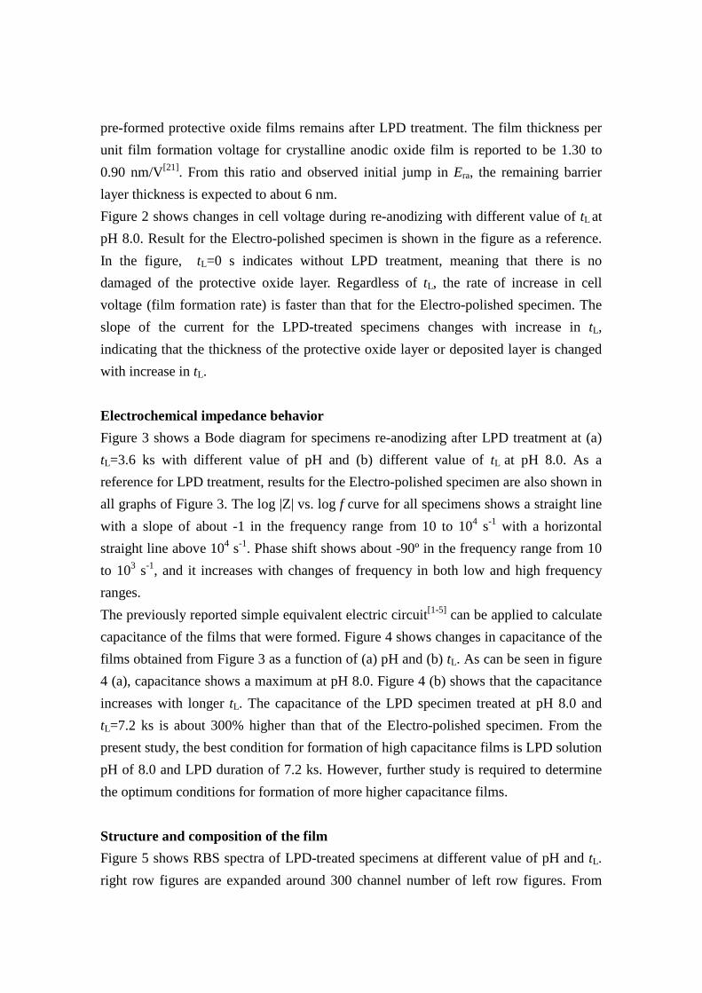
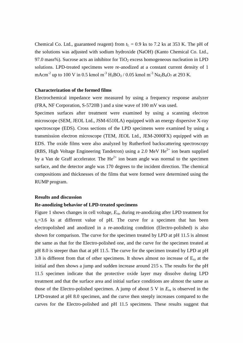
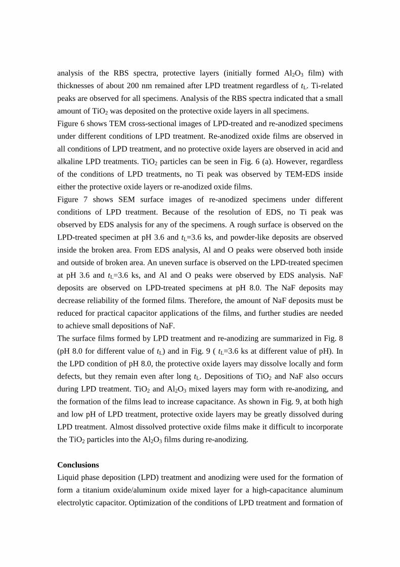
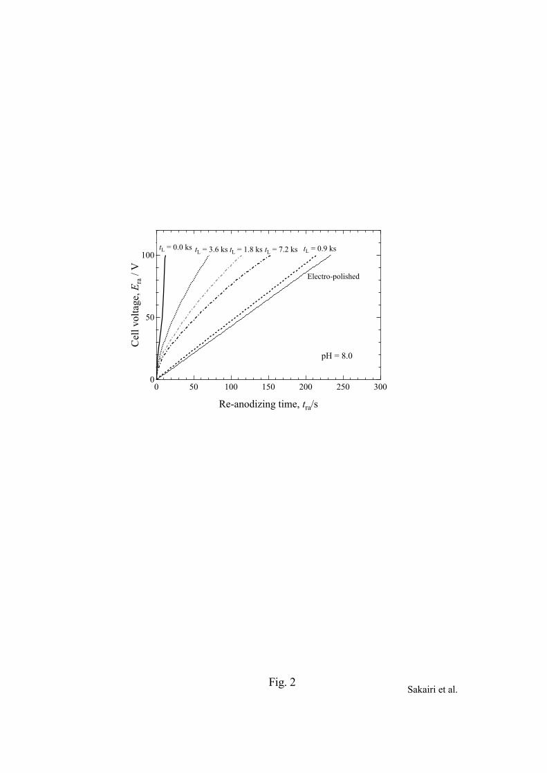
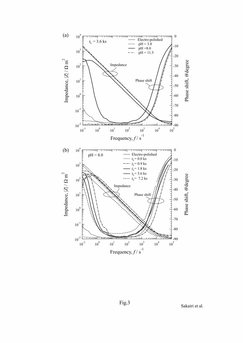
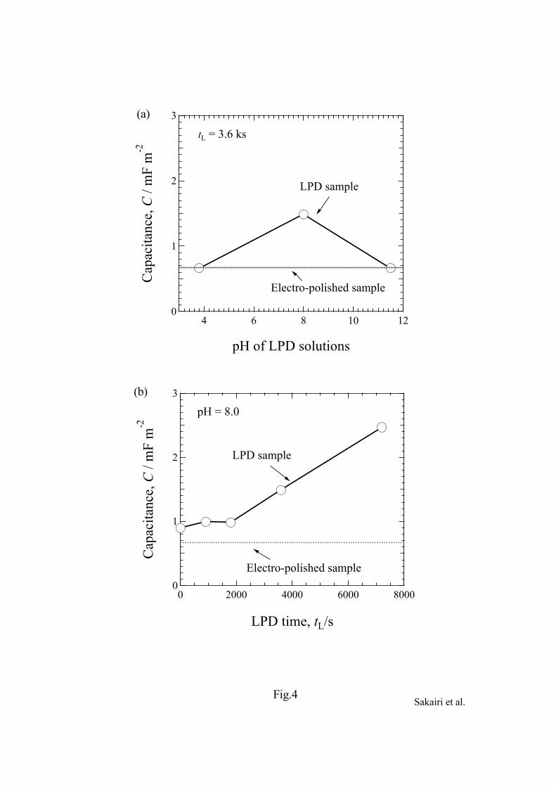
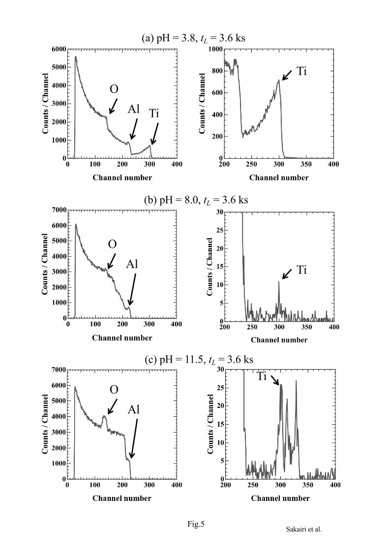
pre-formed protective oxide films remains after LPD treatment. The film thickness per unit film formation voltage for crystalline anodic oxide film is reported to be 1.30 to 0.90 nm/V[21]. From this ratio and observed initial jump in Era, the remaining barrier layer thickness is expected to about 6 nm. Figure 2 shows changes in cell voltage during re-anodizing with different value of tL at pH 8.0. Result for the Electro-polished specimen is shown in the figure as a reference. In the figure, tL=0 s indicates without LPD treatment, meaning that there is no damaged of the protective oxide layer. Regardless of tL, the rate of increase in cell voltage (film formation rate) is faster than that for the Electro-polished specimen. The slope of the current for the LPD-treated specimens changes with increase in tL, indicating that the thickness of the protective oxide layer or deposited layer is changed with increase in tL. Electrochemical impedance behavior Figure 3 shows a Bode diagram for specimens re-anodizing after LPD treatment at (a) tL=3.6 ks with different value of pH and (b) different value of tL at pH 8.0. As a reference for LPD treatment, results for the Electro-polished specimen are also shown in all graphs of Figure 3. The log |Z| vs. log f curve for all specimens shows a straight line with a slope of about -1 in the frequency range from 10 to 104 s-1 with a horizontal straight line above 104 s-1. Phase shift shows about -90º in the frequency range from 10 to 103 s-1, and it increases with changes of frequency in both low and high frequency ranges. The previously reported simple equivalent electric circuit[1-5] can be applied to calculate capacitance of the films that were formed. Figure 4 shows changes in capacitance of the films obtained from Figure 3 as a function of (a) pH and (b) tL. As can be seen in figure 4 (a), capacitance shows a maximum at pH 8.0. Figure 4 (b) shows that the capacitance increases with longer tL. The capacitance of the LPD specimen treated at pH 8.0 and tL=7.2 ks is about 300% higher than that of the Electro-polished specimen. From the present study, the best condition for formation of high capacitance films is LPD solution pH of 8.0 and LPD duration of 7.2 ks. However, further study is required to determine the optimum conditions for formation of more higher capacitance films. Structure and composition of the film Figure 5 shows RBS spectra of LPD-treated specimens at different value of pH and tL. right row figures are expanded around 300 channel number of left row figures. From
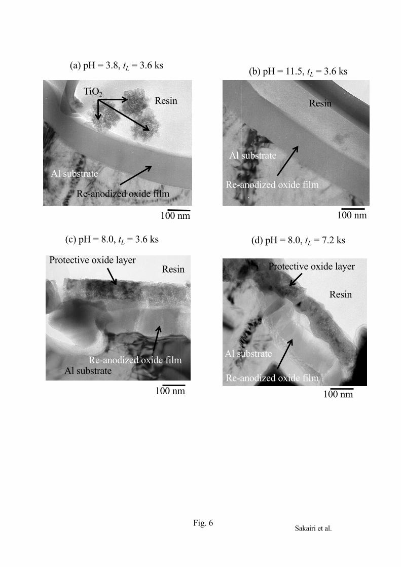
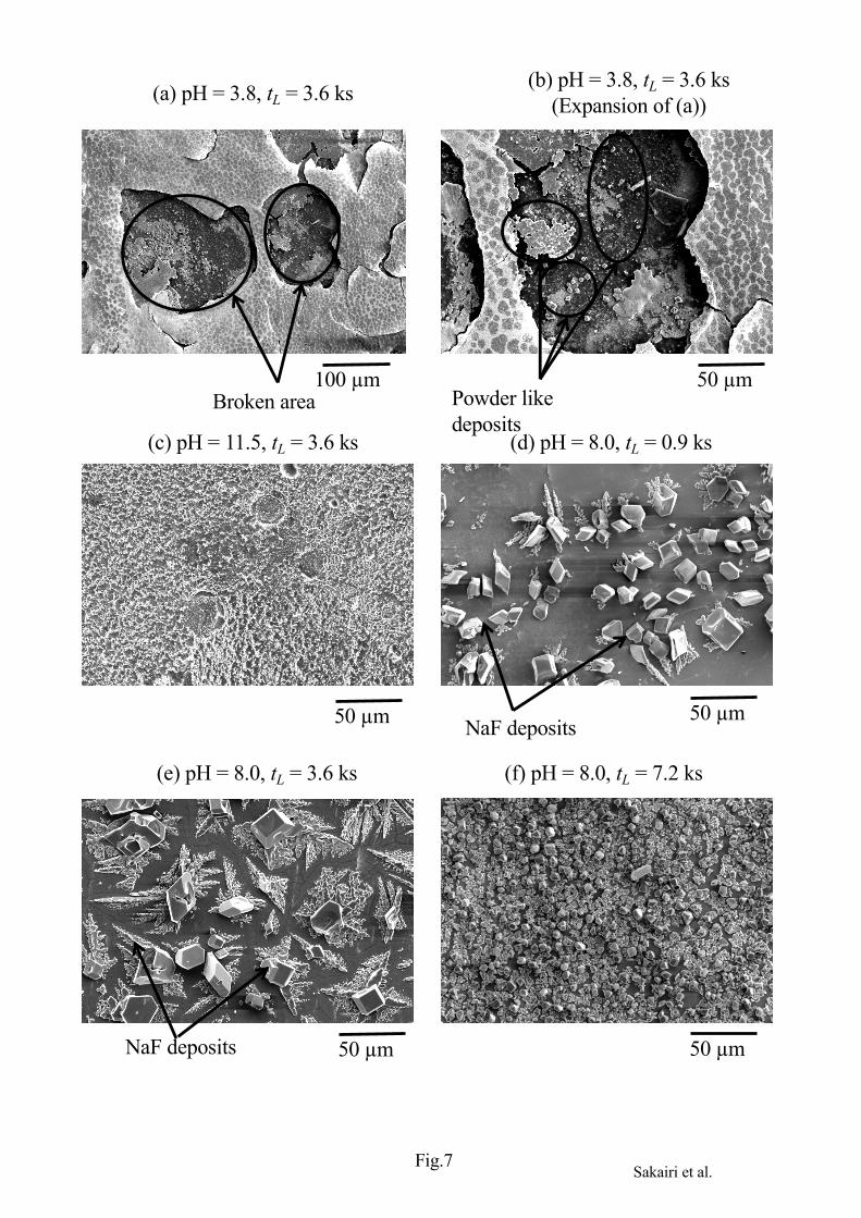
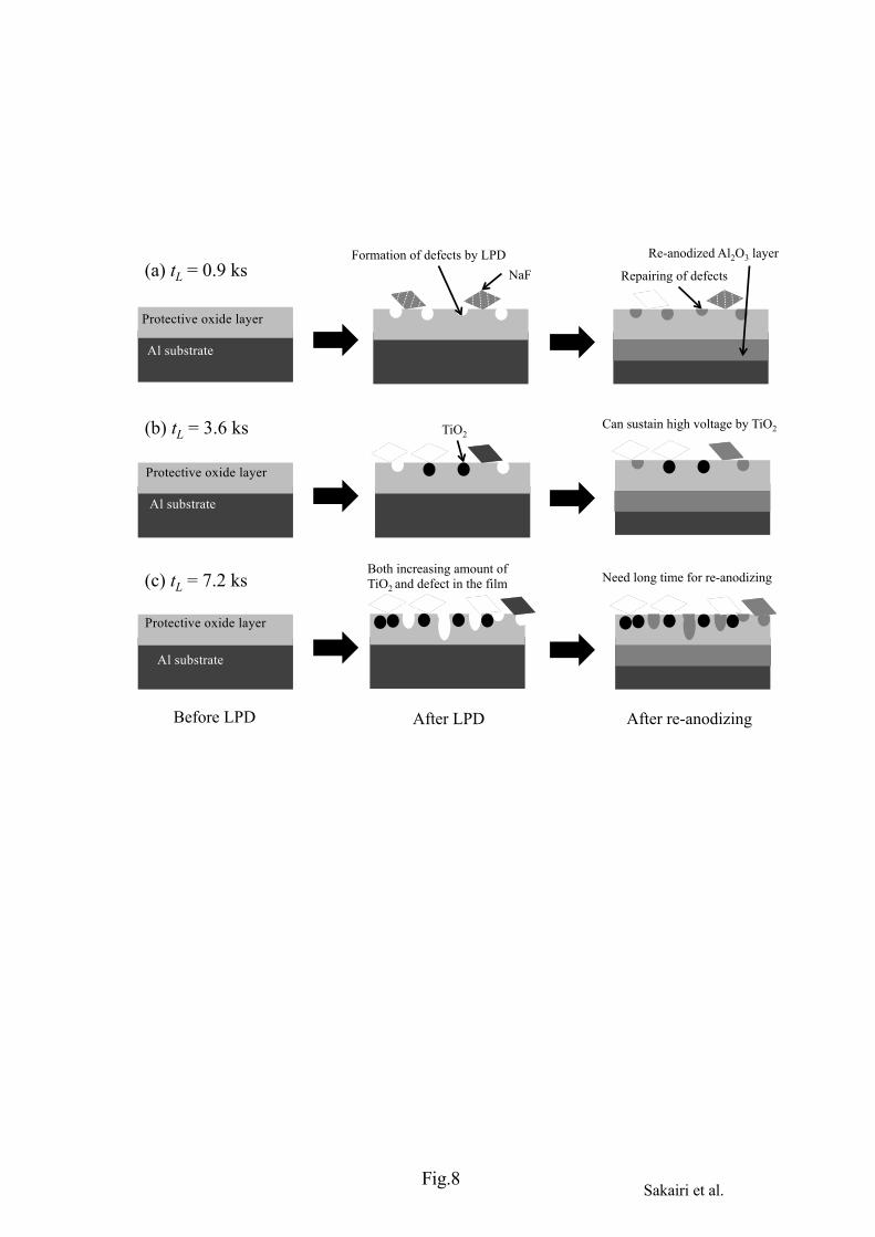
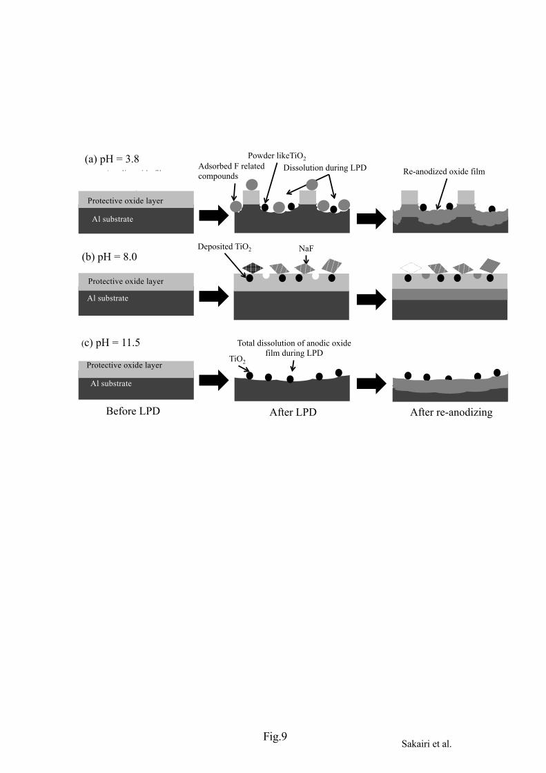
analysis of the RBS spectra, protective layers (initially formed Al2O3 film) with thicknesses of about 200 nm remained after LPD treatment regardless of tL. Ti-related peaks are observed for all specimens. Analysis of the RBS spectra indicated that a small amount of TiO2 was deposited on the protective oxide layers in all specimens. Figure 6 shows TEM cross-sectional images of LPD-treated and re-anodized specimens under different conditions of LPD treatment. Re-anodized oxide films are observed in all conditions of LPD treatment, and no protective oxide layers are observed in acid and alkaline LPD treatments. TiO2 particles can be seen in Fig. 6 (a). However, regardless of the conditions of LPD treatments, no Ti peak was observed by TEM-EDS inside either the protective oxide layers or re-anodized oxide films. Figure 7 shows SEM surface images of re-anodized specimens under different conditions of LPD treatment. Because of the resolution of EDS, no Ti peak was observed by EDS analysis for any of the specimens. A rough surface is observed on the LPD-treated specimen at pH 3.6 and tL=3.6 ks, and powder-like deposits are observed inside the broken area. From EDS analysis, Al and O peaks were observed both inside and outside of broken area. An uneven surface is observed on the LPD-treated specimen at pH 3.6 and tL=3.6 ks, and Al and O peaks were observed by EDS analysis. NaF deposits are observed on LPD-treated specimens at pH 8.0. The NaF deposits may decrease reliability of the formed films. Therefore, the amount of NaF deposits must be reduced for practical capacitor applications of the films, and further studies are needed to achieve small depositions of NaF. The surface films formed by LPD treatment and re-anodizing are summarized in Fig. 8 (pH 8.0 for different value of tL) and in Fig. 9 ( tL=3.6 ks at different value of pH). In the LPD condition of pH 8.0, the protective oxide layers may dissolve locally and form defects, but they remain even after long tL. Depositions of TiO2 and NaF also occurs during LPD treatment. TiO2 and Al2O3 mixed layers may form with re-anodizing, and the formation of the films lead to increase capacitance. As shown in Fig. 9, at both high and low pH of LPD treatment, protective oxide layers may be greatly dissolved during LPD treatment. Almost dissolved protective oxide films make it difficult to incorporate the TiO2 particles into the Al2O3 films during re-anodizing. Conclusions Liquid phase deposition (LPD) treatment and anodizing were used for the formation of form a titanium oxide/aluminum oxide mixed layer for a high-capacitance aluminum electrolytic capacitor. Optimization of the conditions of LPD treatment and formation of
a protective oxide layer make it possible to prolong the LPD duration and lead to the formation of TiO2 and NaF deposits on the aluminum. The capacitance of the formed layer under optimized conditions is about 300% higher than that of an anodic oxide film formed on electropolished aluminum. The results also suggest that reduction of the NaF deposition is required for practical capacitor applications. Acknowledgments A part of this work is financially supported by The Light Metals Educational Foundation Inc.. Reference [1] K. Watanabe, M. Sakairi, H. Takahashi, S. Hirai, S. Yamaguchi, J. Surf. Finish. Soc. Jpn., 1999; 50, 359. [2] K. Watanabe, M. Sakairi, H. Takahashi, S. Hirai, S. Yamaguchi, J. Electroanal. Chem., 1999; 473, 250. [3] K. Watanabe, M. Sakairi, H. Takahashi, K. Takahiro, S. Nagata, S. Hirai, Electrochemistry, 1999; 67, 1243. [4] K. Watanabe, M. Sakairi, H. Takahashi, K. Takahiro, S. Nagata, S. Hirai, Electrochemistry, 2001; 69, 407. [5] K. Watanabe, M. Sakairi, H. Takahashi, K. Takahiro, S. Nagata, S. Hirai, J. Electrochem. Soc., 2001; 148, B473. [6] S. Koyama, T. Kikuchi, M. Sakairi, H. Takahashi, S. Nagata, Electrochemistry, 2007; 75, 573. [7] M. Sunada, T. Kikuchi, M. Sakairi, H. Takahashi, S. Hirai, J. Solid State Elecherochm., 2007; 11, 1375. [8] L. Yao, J. Liu, M. Yu, S. Li, H. Wu, Trans. Nonferrous Metals Soc. of China, 2010; 20, 825. [9] X. Du, Y. Xu, Thin Solid Films, 2008; 516, 8436. [10] S. Deki, Y. Aoi, O. Hiroi, A. Kajinami, Chem. Lett., 1996; 25, 433. [11] S. Deki, S. Iizuka, A. Horie, M. Mizuhata, A. Kajinami, Chem. Mater., 2004; 16, 1747. [12] J. Huang and Y. Lee, Surface & coating technology, 2013; 231, 257. [13] M. Mizuhata, A. Katayama, H. Maki, ECS Trans., 2014; 61, 9. [14] M. Mizuhata, A. Katayama, H. Maki, J. Flourine Chem., 2015; 174, 62.
[15] T. Wu, C. Hu, P. Sze, T. Huang, F. Adriyato, C. Wu and Y. Wang, Solid-State Electronics, 2013; 82, 1. [16] C. X. Lei, H. Zhou, Z. D. Feng, Y. F. Zhu, R. G. Du, J. Alloy and Compounds, 2012; 513, 552. [17] S. C. Lee, H. Yu, J. Yu, C.H. Ao, J. Cryst. Growth, 2006; 295, 60. [18] M. Sakairi, R. Fujita, T. Kikuchi, S. Nagata, Proc. of 5th Int. Sympo. Marine Corros. and Control, Qingdo, 2011; 277. [19] R. Fujita, M. Sakairi, T. Kikuchi, Electorochim. Acta, 2011; 56, 7180. [20] M. Sakairi, R. Fujita, H. Jha, T. Kikuchi, Surface and Interface Analysis special Issue of ASST2012, 2013; 45, 1510. [21] H. Takahashi, Y Umehara, T. Miyamoto, N. Fujimoto, M. Nagayama, J. Surf. Fin. Soc. Jpn., 1987; 38, 66.
Caption list Fig. 1 Changes in cell voltage, Era, during re-anodizing after LPD treatment for tL=3.6 ks at different value of pH. Fig. 2 Changes in cell voltage during re-anodizing with different tL at pH 8.0. Fig. 3 Bode diagram for specimens re-anodizing after LPD treatment at (a) tL=3.6 ks with different value of pH and (b) different value of tL at pH 8.0. Fig. 4 Changes in capacitance of the formed films obtained from Figure 3 as a function of (a) pH and (b) tL. Fig. 5 RBS spectra of LPD treated specimens at different pH and tL. Fig. 6 TEM cross-sectional images of LPD-treated and re-anodized specimens under different conditions of LPD treatment. Fig. 7 SEM surface images of LPD treated and re-anodized specimens at different LPD conditions. Fig. 8 Summary of films formed by LPD and re-anodizing treatments at pH 8.0 for different tL Fig. 9 Summary of films formed by LPD and re-anodizing treatments for tL=3.6 ks at different pH.
100
50
0
Cel
l vol
tage
, Era
/ V
300250200150100500
Anodizing time, tra/s
pH = 3.8pH = 8.0 pH = 11.5
Electro-polished
tL=3.6 ks
Fig. 1Sakairi et al.
100
50
0
Cel
l vol
tage
, Era
/ V
300250200150100500
Re-anodizing time, tra/s
tL = 0.0 ks tL = 0.9 ks
Electro-polished
tL = 1.8 kstL = 3.6 ks tL = 7.2 ks
pH = 8.0
Fig. 2Sakairi et al.
10-2
10-1
100
101
102
103
104
Impe
danc
e, | Z
| / Ω
m2
10-1 100 101 102 103 104 105
Frequency, f / s-1
-90
-80
-70
-60
-50
-40
-30
-20
-10
0
Phas
e sh
ift, θ
/deg
ree
Electro-polished pH = 3.8 pH =8.0 pH = 11.5
Impedance
Phase shift
tL = 3.6 ks
10-2
10-1
100
101
102
103
104
Impe
danc
e, | Z
| / Ω
m2
10-1 100 101 102 103 104 105
Frequency, f / s-1
-90
-80
-70
-60
-50
-40
-30
-20
-10
0
Phas
e sh
ift, θ/degree
Electro-polished tL= 0.0 ks tL= 0.9 ks tL= 1.8 ks tL= 3.6 ks tL= 7.2 ks
Impedance
Phase shift
pH = 8.0
(a)
(b)
Fig.3Sakairi et al.
3
2
1
0
Cap
acita
nce,
C /
mF
m-2
1210864
pH of LPD solutions
LPD sample
Electro-polished sample
tL = 3.6 ks
3
2
1
0
Cap
acita
nce,
C /
mF
m-2
80006000400020000
LPD time, tL/s
LPD sample
Electro-polished sample
pH = 8.0
(a)
(b)
Fig.4Sakairi et al.
(a) pH = 3.8, tL = 3.6 ks
(b) pH = 8.0, tL = 3.6 ks
(c) pH = 11.5, tL = 3.6 ks
TiAlO
Ti
AlO
Ti
AlO
Ti
Fig.5Sakairi et al.
(d) pH = 8.0, tL = 3.6 ks
(a) pH = 3.8, tL = 3.6 ks
100 nm
Resin
Al substrate
Re-anodized oxide film
TiO2
(b) pH = 11.5, tL = 3.6 ks
100 nm
Resin
Al substrate
Re-anodized oxide film
100 nm
Resin
Al substrate
Protective oxide layer
Re-anodized oxide film
(c) pH = 8.0, tL = 3.6 ks (d) pH = 8.0, tL = 7.2 ks
Re-anodized oxide film
Protective oxide layer
Al substrate
Resin
100 nm
Fig. 6Sakairi et al.
50 µm
50 µm 50 µm
50 µm 50 µm
(a) pH = 3.8, tL = 3.6 ks
(c) pH = 11.5, tL = 3.6 ks (d) pH = 8.0, tL = 0.9 ks
(e) pH = 8.0, tL = 3.6 ks (f) pH = 8.0, tL = 7.2 ks
100 µm
(b) pH = 3.8, tL = 3.6 ks(Expansion of (a))
Powder like deposits
Broken area
NaF deposits
NaF deposits
Fig.7Sakairi et al.
Formation of defects by LPD�NaF�
TiO2�
Both increasing amount of TiO2 and defect in the film �
(a) tL = 0.9 ks�
Can sustain high voltage by TiO2�
Need long time for re-anodizing
Before LPD� After LPD� After re-anodizing�
(b) tL = 3.6 ks�
(c) tL = 7.2 ks�
Repairing of defects�
Re-anodized Al2O3 layer�
Protective oxide layer
Protective oxide layer
Protective oxide layer
Al substrate
Al substrate
Al substrate
Fig.8Sakairi et al.
(b) pH = 8.0�
(a) pH = 3.8�
(c) pH = 11.5�
Anodic oxide film�
Powder likeTiO2�
Before LPD� After LPD�
NaF�Deposited TiO2�
Total dissolution of anodic oxide film during LPD�
Dissolution during LPD�
TiO2�
Adsorbed F related compounds��
After re-anodizing�
Re-anodized oxide film�
Al substrate
Al substrate
Al substrate
Protective oxide layer
Protective oxide layer
Protective oxide layer
Fig.9Sakairi et al.