foldable world_update
TRANSCRIPT
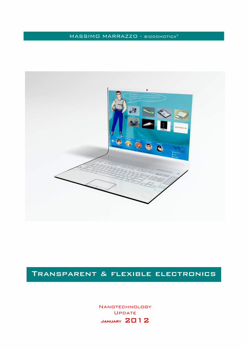
NanotechnologyUpdate
JanuaryJanuaryJanuaryJanuary 2012 2012 2012 2012
Transparent & flexible electronics
MASSIMO MARRAZZO - BIODOMOTICA®
Transparent & Flexible Electronics
2 Massimo Marrazzo - biodomotica.com
IIIIIIIInnnnnnnnddddddddeeeeeeeexxxxxxxx
Transparent electronics pag.3Touch-screen display 6Stretchable electronics 8Transparent batteries 10Printed electronics 14Electronic paper / E-paper 18Plastic Electronics 22
Links 25Show/Convention/Exposition 26
2012 Update 27
TTTTTTTTrrrrrrrraaaaaaaannnnnnnnssssssssppppppppaaaaaaaarrrrrrrreeeeeeeennnnnnnntttttttt EEEEEEEElllllllleeeeeeeeccccccccttttttttrrrrrrrroooooooonnnnnnnniiiiiiiiccccccccssssssss
- http://ewandoo.com/samsung-electronics-produced-22-inch-transparent-lcd/
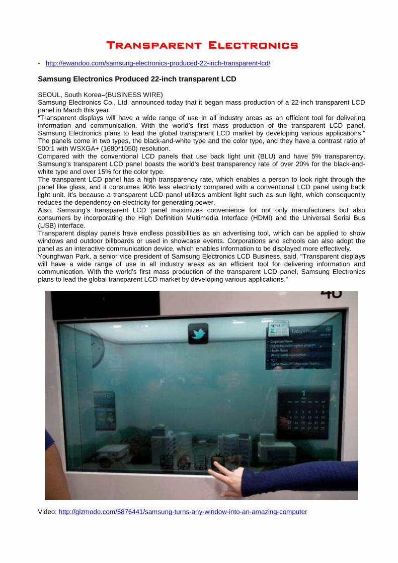
Samsung Electronics Produced 22-inch transparent LC D
SEOUL, South Korea–(BUSINESS WIRE)Samsung Electronics Co., Ltd. announced today that it began mass production of a 22-inch transparent LCDpanel in March this year.“Transparent displays will have a wide range of use in all industry areas as an efficient tool for deliveringinformation and communication. With the world’s first mass production of the transparent LCD panel,Samsung Electronics plans to lead the global transparent LCD market by developing various applications.”The panels come in two types, the black-and-white type and the color type, and they have a contrast ratio of500:1 with WSXGA+ (1680*1050) resolution.Compared with the conventional LCD panels that use back light unit (BLU) and have 5% transparency,Samsung’s transparent LCD panel boasts the world’s best transparency rate of over 20% for the black-and-white type and over 15% for the color type.The transparent LCD panel has a high transparency rate, which enables a person to look right through thepanel like glass, and it consumes 90% less electricity compared with a conventional LCD panel using backlight unit. It’s because a transparent LCD panel utilizes ambient light such as sun light, which consequentlyreduces the dependency on electricity for generating power.Also, Samsung’s transparent LCD panel maximizes convenience for not only manufacturers but alsoconsumers by incorporating the High Definition Multimedia Interface (HDMI) and the Universal Serial Bus(USB) interface.Transparent display panels have endless possibilities as an advertising tool, which can be applied to showwindows and outdoor billboards or used in showcase events. Corporations and schools can also adopt thepanel as an interactive communication device, which enables information to be displayed more effectively.Younghwan Park, a senior vice president of Samsung Electronics LCD Business, said, “Transparent displayswill have a wide range of use in all industry areas as an efficient tool for delivering information andcommunication. With the world’s first mass production of the transparent LCD panel, Samsung Electronicsplans to lead the global transparent LCD market by developing various applications.”
Video: http://gizmodo.com/5876441/samsung-turns-any-window-into-an-amazing-computer
Transparent & Flexible Electronics
4 Massimo Marrazzo - biodomotica.com
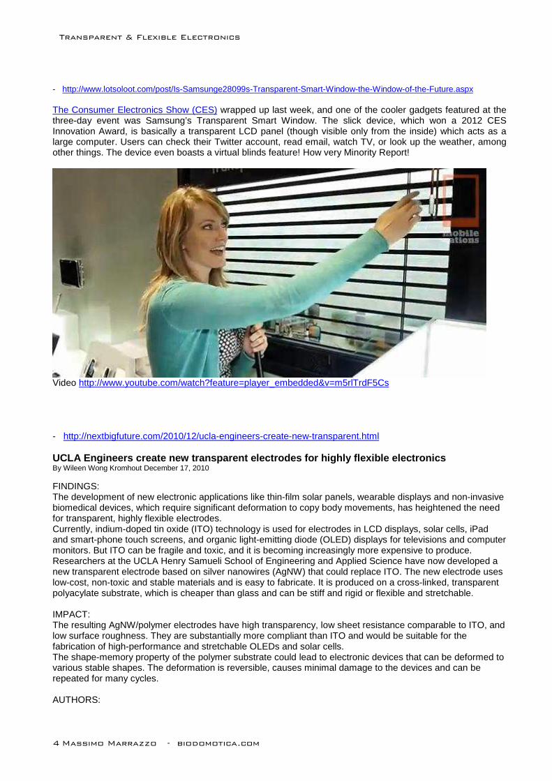
- http://www.lotsoloot.com/post/Is-Samsunge28099s-Transparent-Smart-Window-the-Window-of-the-Future.aspx
The Consumer Electronics Show (CES) wrapped up last week, and one of the cooler gadgets featured at thethree-day event was Samsung’s Transparent Smart Window. The slick device, which won a 2012 CESInnovation Award, is basically a transparent LCD panel (though visible only from the inside) which acts as alarge computer. Users can check their Twitter account, read email, watch TV, or look up the weather, amongother things. The device even boasts a virtual blinds feature! How very Minority Report!
Video http://www.youtube.com/watch?feature=player_embedded&v=m5rlTrdF5Cs
- http://nextbigfuture.com/2010/12/ucla-engineers-create-new-transparent.html
UCLA Engineers create new transparent electrodes fo r highly flexible electronicsBy Wileen Wong Kromhout December 17, 2010
FINDINGS:The development of new electronic applications like thin-film solar panels, wearable displays and non-invasivebiomedical devices, which require significant deformation to copy body movements, has heightened the needfor transparent, highly flexible electrodes.Currently, indium-doped tin oxide (ITO) technology is used for electrodes in LCD displays, solar cells, iPadand smart-phone touch screens, and organic light-emitting diode (OLED) displays for televisions and computermonitors. But ITO can be fragile and toxic, and it is becoming increasingly more expensive to produce.Researchers at the UCLA Henry Samueli School of Engineering and Applied Science have now developed anew transparent electrode based on silver nanowires (AgNW) that could replace ITO. The new electrode useslow-cost, non-toxic and stable materials and is easy to fabricate. It is produced on a cross-linked, transparentpolyacylate substrate, which is cheaper than glass and can be stiff and rigid or flexible and stretchable.
IMPACT:The resulting AgNW/polymer electrodes have high transparency, low sheet resistance comparable to ITO, andlow surface roughness. They are substantially more compliant than ITO and would be suitable for thefabrication of high-performance and stretchable OLEDs and solar cells.The shape-memory property of the polymer substrate could lead to electronic devices that can be deformed tovarious stable shapes. The deformation is reversible, causes minimal damage to the devices and can berepeated for many cycles.
AUTHORS:
Authors of the research are Zhibin Yu, Qingwu Zhang, Lu Li, Qi Chen, Xiaofan Niu, Jun Liu and Qibing Pei.The invention of the new transparent electrode was led by Qibing Pei, who is a professor of materials scienceand engineering at UCLA Engineering.
FUNDING:The research was partially supported by the U.S. Department of Energy's Solid-State Lighting program and bythe National Science Foundation.
JOURNAL:This research was recently published in the peer-reviewed journal Advanced Materials and is available onlineat: http://onlinelibrary.wiley.com/doi/10.1002/adma.201003398/abstract.
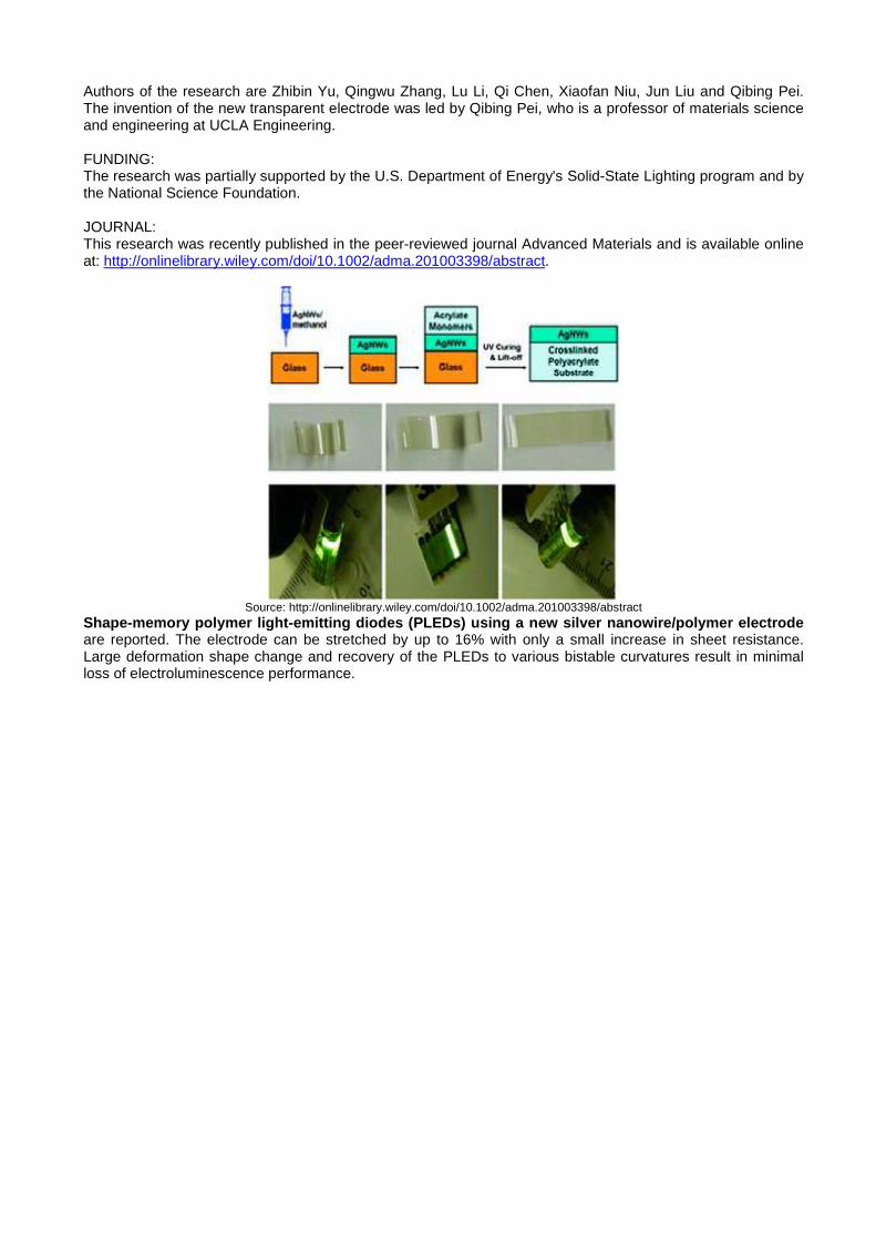
Source: http://onlinelibrary.wiley.com/doi/10.1002/adma.201003398/abstractShape-memory polymer light-emitting diodes (PLEDs) using a new silver nanowire/polymer electrodeare reported. The electrode can be stretched by up to 16% with only a small increase in sheet resistance.Large deformation shape change and recovery of the PLEDs to various bistable curvatures result in minimalloss of electroluminescence performance.
Transparent & Flexible Electronics
6 Massimo Marrazzo - biodomotica.com
TTTTTTTToooooooouuuuuuuucccccccchhhhhhhh--------ssssssssccccccccrrrrrrrreeeeeeeeeeeeeeeennnnnnnn ddddddddiiiiiiiissssssssppppppppllllllllaaaaaaaayyyyyyyyssssssss
- http://www.media.rice.edu/media/NewsBot.asp?MODE=VIEW&ID=16008
Dream screens from grapheneTechnology developed at Rice could revolutionize to uch-screen displaysBY MIKE WILLIAMS Rice News staff - 8/2/2011
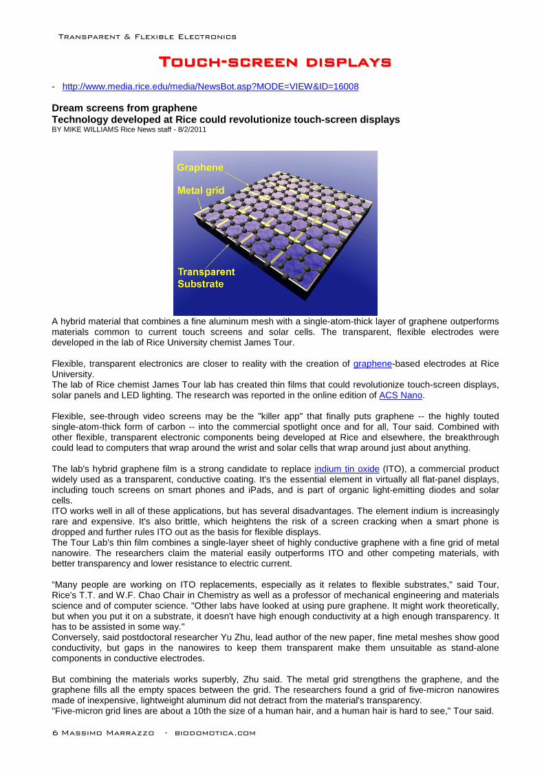
A hybrid material that combines a fine aluminum mesh with a single-atom-thick layer of graphene outperformsmaterials common to current touch screens and solar cells. The transparent, flexible electrodes weredeveloped in the lab of Rice University chemist James Tour.
Flexible, transparent electronics are closer to reality with the creation of graphene-based electrodes at RiceUniversity.The lab of Rice chemist James Tour lab has created thin films that could revolutionize touch-screen displays,solar panels and LED lighting. The research was reported in the online edition of ACS Nano.
Flexible, see-through video screens may be the "killer app" that finally puts graphene -- the highly toutedsingle-atom-thick form of carbon -- into the commercial spotlight once and for all, Tour said. Combined withother flexible, transparent electronic components being developed at Rice and elsewhere, the breakthroughcould lead to computers that wrap around the wrist and solar cells that wrap around just about anything.
The lab's hybrid graphene film is a strong candidate to replace indium tin oxide (ITO), a commercial productwidely used as a transparent, conductive coating. It's the essential element in virtually all flat-panel displays,including touch screens on smart phones and iPads, and is part of organic light-emitting diodes and solarcells.ITO works well in all of these applications, but has several disadvantages. The element indium is increasinglyrare and expensive. It's also brittle, which heightens the risk of a screen cracking when a smart phone isdropped and further rules ITO out as the basis for flexible displays.The Tour Lab's thin film combines a single-layer sheet of highly conductive graphene with a fine grid of metalnanowire. The researchers claim the material easily outperforms ITO and other competing materials, withbetter transparency and lower resistance to electric current.
“Many people are working on ITO replacements, especially as it relates to flexible substrates," said Tour,Rice's T.T. and W.F. Chao Chair in Chemistry as well as a professor of mechanical engineering and materialsscience and of computer science. "Other labs have looked at using pure graphene. It might work theoretically,but when you put it on a substrate, it doesn't have high enough conductivity at a high enough transparency. Ithas to be assisted in some way."Conversely, said postdoctoral researcher Yu Zhu, lead author of the new paper, fine metal meshes show goodconductivity, but gaps in the nanowires to keep them transparent make them unsuitable as stand-alonecomponents in conductive electrodes.
But combining the materials works superbly, Zhu said. The metal grid strengthens the graphene, and thegraphene fills all the empty spaces between the grid. The researchers found a grid of five-micron nanowiresmade of inexpensive, lightweight aluminum did not detract from the material's transparency."Five-micron grid lines are about a 10th the size of a human hair, and a human hair is hard to see," Tour said.
Tour said metal grids could be easily produced on a flexible substrate via standard techniques, including roll-to-roll and ink-jet printing. Techniques for making large sheets of graphene are also improving rapidly, he said;commercial labs have already developed a roll-to-roll graphene production technique."This material is ready to scale right now," he said.The flexibility is almost a bonus, Zhu said, due to the potential savings of using carbon and aluminum insteadof expensive ITO. "Right now, ITO is the only commercial electrode we have, but it's brittle," he said. "Ourtransparent electrode has better conductivity than ITO and it's flexible. I think flexible electronics will benefit alot."In tests, he found the hybrid film's conductivity decreases by 20 to 30 percent with the initial 50 bends, butafter that, the material stabilizes. "There were no significant variations up to 500 bending cycles," Zhu said.More rigorous bending test will be left to commercial users, he said.
“I don't know how many times a person would roll up a computer," Tour added. "Maybe 1,000 times? Tenthousand times? It's hard to see how it would wear out in the lifetime you would normally keep a device."The film also proved environmentally stable. When the research paper was submitted in late 2010, test filmshad been exposed to the environment in the lab for six months without deterioration. After a year, they remainso."Now that we know it works fine on flexible substrates, this brings the efficacy of graphene a step up to itspotential utility," Tour said.Rice graduate students Zhengzong Sun and Zheng Yan and former postdoctoral researcher Zhong Jin are co-authors of the paper.
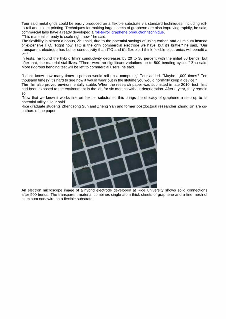
An electron microscope image of a hybrid electrode developed at Rice University shows solid connectionsafter 500 bends. The transparent material combines single-atom-thick sheets of graphene and a fine mesh ofaluminum nanowire on a flexible substrate.
Transparent & Flexible Electronics
8 Massimo Marrazzo - biodomotica.com
SSSSSSSSttttttttrrrrrrrreeeeeeeettttttttcccccccchhhhhhhhaaaaaaaabbbbbbbblllllllleeeeeeee EEEEEEEElllllllleeeeeeeeccccccccttttttttrrrrrrrroooooooonnnnnnnniiiiiiiiccccccccssssssss
- http://www.physorg.com/news/2011-10-stretchable-graphene-transistors-limitations-materials.html
Stretchable graphene transistors overcome limitatio ns of other materialsOctober 26, 2011 by Lisa Zyga
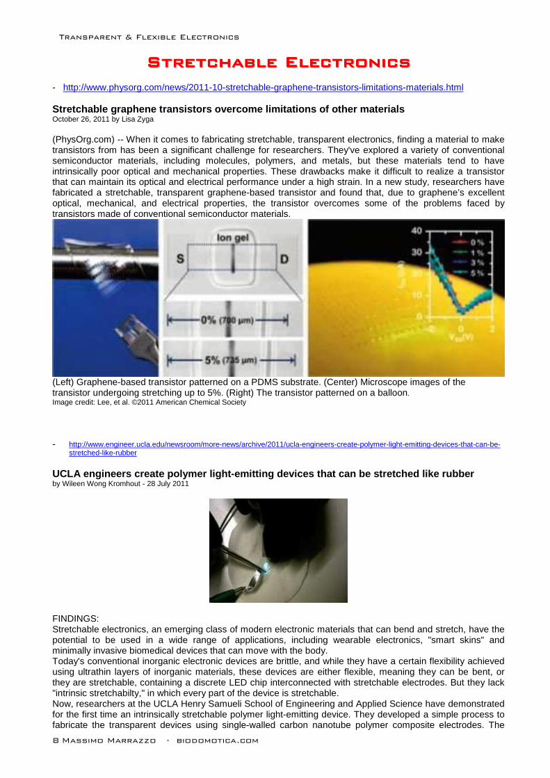
(PhysOrg.com) -- When it comes to fabricating stretchable, transparent electronics, finding a material to maketransistors from has been a significant challenge for researchers. They've explored a variety of conventionalsemiconductor materials, including molecules, polymers, and metals, but these materials tend to haveintrinsically poor optical and mechanical properties. These drawbacks make it difficult to realize a transistorthat can maintain its optical and electrical performance under a high strain. In a new study, researchers havefabricated a stretchable, transparent graphene-based transistor and found that, due to graphene’s excellentoptical, mechanical, and electrical properties, the transistor overcomes some of the problems faced bytransistors made of conventional semiconductor materials.
(Left) Graphene-based transistor patterned on a PDMS substrate. (Center) Microscope images of thetransistor undergoing stretching up to 5%. (Right) The transistor patterned on a balloon.Image credit: Lee, et al. ©2011 American Chemical Society
- http://www.engineer.ucla.edu/newsroom/more-news/archive/2011/ucla-engineers-create-polymer-light-emitting-devices-that-can-be-stretched-like-rubber
UCLA engineers create polymer light-emitting device s that can be stretched like rubberby Wileen Wong Kromhout - 28 July 2011
FINDINGS:Stretchable electronics, an emerging class of modern electronic materials that can bend and stretch, have thepotential to be used in a wide range of applications, including wearable electronics, "smart skins" andminimally invasive biomedical devices that can move with the body.Today's conventional inorganic electronic devices are brittle, and while they have a certain flexibility achievedusing ultrathin layers of inorganic materials, these devices are either flexible, meaning they can be bent, orthey are stretchable, containing a discrete LED chip interconnected with stretchable electrodes. But they lack"intrinsic stretchabilty," in which every part of the device is stretchable.Now, researchers at the UCLA Henry Samueli School of Engineering and Applied Science have demonstratedfor the first time an intrinsically stretchable polymer light-emitting device. They developed a simple process tofabricate the transparent devices using single-walled carbon nanotube polymer composite electrodes. The
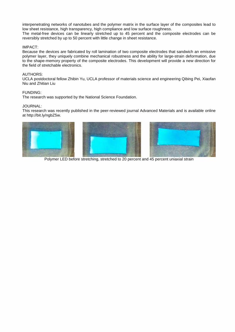
interpenetrating networks of nanotubes and the polymer matrix in the surface layer of the composites lead tolow sheet resistance, high transparency, high compliance and low surface roughness.The metal-free devices can be linearly stretched up to 45 percent and the composite electrodes can bereversibly stretched by up to 50 percent with little change in sheet resistance.
IMPACT:Because the devices are fabricated by roll lamination of two composite electrodes that sandwich an emissivepolymer layer, they uniquely combine mechanical robustness and the ability for large-strain deformation, dueto the shape-memory property of the composite electrodes. This development will provide a new direction forthe field of stretchable electronics.
AUTHORS:UCLA postdoctoral fellow Zhibin Yu, UCLA professor of materials science and engineering Qibing Pei, XiaofanNiu and Zhitian Liu
FUNDING:The research was supported by the National Science Foundation.
JOURNAL:This research was recently published in the peer-reviewed journal Advanced Materials and is available onlineat http://bit.ly/ngbZ5w.
Polymer LED before stretching, stretched to 20 percent and 45 percent uniaxial strain
Transparent & Flexible Electronics
10 Massimo Marrazzo - biodomotica.com
TTTTTTTTrrrrrrrraaaaaaaannnnnnnnssssssssppppppppaaaaaaaarrrrrrrreeeeeeeennnnnnnntttttttt BBBBBBBBaaaaaaaatttttttttttttttteeeeeeeerrrrrrrriiiiiiiieeeeeeeessssssss
- http://www.innovationnewsdaily.com/454-transparent-batteries.html
Transparent Batteries Help Mobile Devices Go See-Th roughCharles Choi, InnovationNewsDaily Contributor -25 July 2011
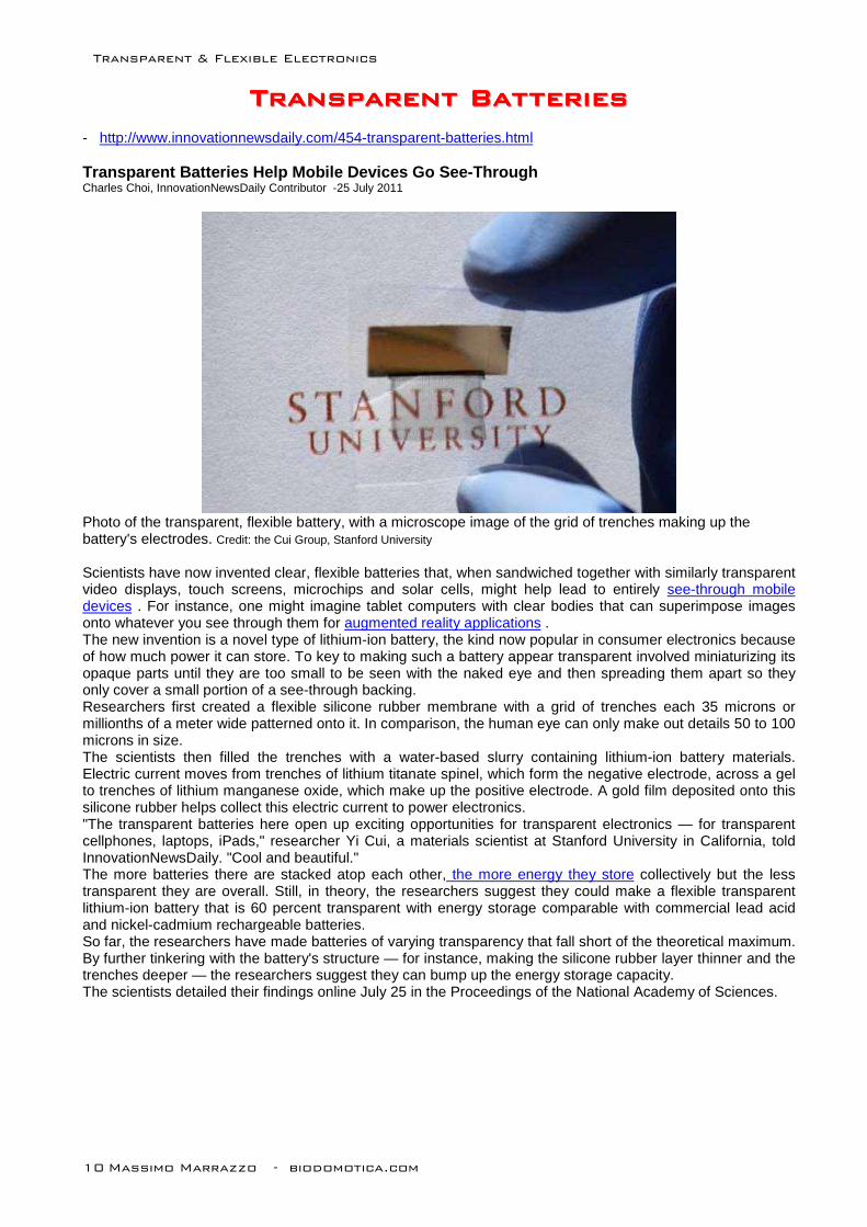
Photo of the transparent, flexible battery, with a microscope image of the grid of trenches making up thebattery's electrodes. Credit: the Cui Group, Stanford University
Scientists have now invented clear, flexible batteries that, when sandwiched together with similarly transparentvideo displays, touch screens, microchips and solar cells, might help lead to entirely see-through mobiledevices . For instance, one might imagine tablet computers with clear bodies that can superimpose imagesonto whatever you see through them for augmented reality applications .The new invention is a novel type of lithium-ion battery, the kind now popular in consumer electronics becauseof how much power it can store. To key to making such a battery appear transparent involved miniaturizing itsopaque parts until they are too small to be seen with the naked eye and then spreading them apart so theyonly cover a small portion of a see-through backing.Researchers first created a flexible silicone rubber membrane with a grid of trenches each 35 microns ormillionths of a meter wide patterned onto it. In comparison, the human eye can only make out details 50 to 100microns in size.The scientists then filled the trenches with a water-based slurry containing lithium-ion battery materials.Electric current moves from trenches of lithium titanate spinel, which form the negative electrode, across a gelto trenches of lithium manganese oxide, which make up the positive electrode. A gold film deposited onto thissilicone rubber helps collect this electric current to power electronics."The transparent batteries here open up exciting opportunities for transparent electronics — for transparentcellphones, laptops, iPads," researcher Yi Cui, a materials scientist at Stanford University in California, toldInnovationNewsDaily. "Cool and beautiful."The more batteries there are stacked atop each other, the more energy they store collectively but the lesstransparent they are overall. Still, in theory, the researchers suggest they could make a flexible transparentlithium-ion battery that is 60 percent transparent with energy storage comparable with commercial lead acidand nickel-cadmium rechargeable batteries.So far, the researchers have made batteries of varying transparency that fall short of the theoretical maximum.By further tinkering with the battery's structure — for instance, making the silicone rubber layer thinner and thetrenches deeper — the researchers suggest they can bump up the energy storage capacity.The scientists detailed their findings online July 25 in the Proceedings of the National Academy of Sciences.
- http://news.stanford.edu/news/2011/july/transparent-litiumion-battery-072511.html
Stanford transparent batteries: seeing straight thr ough to the future?Stanford Report, July 25, 2011
Stanford researchers have invented a transparent lithium-ion battery that is also highly flexible.It is comparable in cost to regular batteries on the market today, with great potential for applications inconsumer electronics.
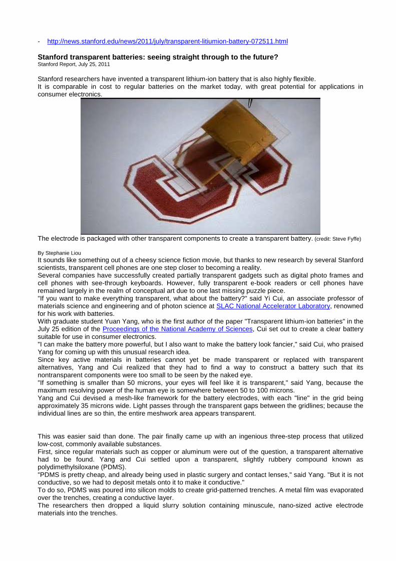
The electrode is packaged with other transparent components to create a transparent battery. (credit: Steve Fyffe)
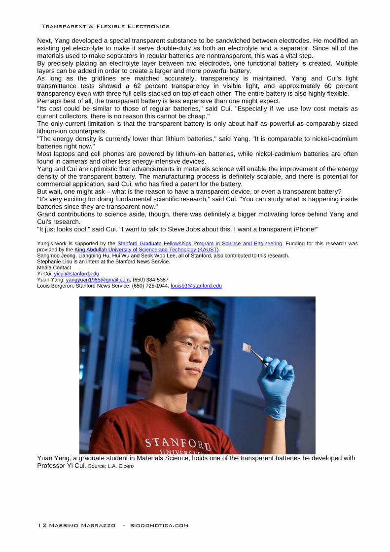
By Stephanie LiouIt sounds like something out of a cheesy science fiction movie, but thanks to new research by several Stanfordscientists, transparent cell phones are one step closer to becoming a reality.Several companies have successfully created partially transparent gadgets such as digital photo frames andcell phones with see-through keyboards. However, fully transparent e-book readers or cell phones haveremained largely in the realm of conceptual art due to one last missing puzzle piece."If you want to make everything transparent, what about the battery?" said Yi Cui, an associate professor ofmaterials science and engineering and of photon science at SLAC National Accelerator Laboratory, renownedfor his work with batteries.With graduate student Yuan Yang, who is the first author of the paper "Transparent lithium-ion batteries" in theJuly 25 edition of the Proceedings of the National Academy of Sciences, Cui set out to create a clear batterysuitable for use in consumer electronics."I can make the battery more powerful, but I also want to make the battery look fancier," said Cui, who praisedYang for coming up with this unusual research idea.Since key active materials in batteries cannot yet be made transparent or replaced with transparentalternatives, Yang and Cui realized that they had to find a way to construct a battery such that itsnontransparent components were too small to be seen by the naked eye."If something is smaller than 50 microns, your eyes will feel like it is transparent," said Yang, because themaximum resolving power of the human eye is somewhere between 50 to 100 microns.Yang and Cui devised a mesh-like framework for the battery electrodes, with each "line" in the grid beingapproximately 35 microns wide. Light passes through the transparent gaps between the gridlines; because theindividual lines are so thin, the entire meshwork area appears transparent.
This was easier said than done. The pair finally came up with an ingenious three-step process that utilizedlow-cost, commonly available substances.First, since regular materials such as copper or aluminum were out of the question, a transparent alternativehad to be found. Yang and Cui settled upon a transparent, slightly rubbery compound known aspolydimethylsiloxane (PDMS)."PDMS is pretty cheap, and already being used in plastic surgery and contact lenses," said Yang. "But it is notconductive, so we had to deposit metals onto it to make it conductive."To do so, PDMS was poured into silicon molds to create grid-patterned trenches. A metal film was evaporatedover the trenches, creating a conductive layer.The researchers then dropped a liquid slurry solution containing minuscule, nano-sized active electrodematerials into the trenches.
Transparent & Flexible Electronics
12 Massimo Marrazzo - biodomotica.com
Next, Yang developed a special transparent substance to be sandwiched between electrodes. He modified anexisting gel electrolyte to make it serve double-duty as both an electrolyte and a separator. Since all of thematerials used to make separators in regular batteries are nontransparent, this was a vital step.By precisely placing an electrolyte layer between two electrodes, one functional battery is created. Multiplelayers can be added in order to create a larger and more powerful battery.As long as the gridlines are matched accurately, transparency is maintained. Yang and Cui's lighttransmittance tests showed a 62 percent transparency in visible light, and approximately 60 percenttransparency even with three full cells stacked on top of each other. The entire battery is also highly flexible.Perhaps best of all, the transparent battery is less expensive than one might expect."Its cost could be similar to those of regular batteries," said Cui. "Especially if we use low cost metals ascurrent collectors, there is no reason this cannot be cheap."The only current limitation is that the transparent battery is only about half as powerful as comparably sizedlithium-ion counterparts."The energy density is currently lower than lithium batteries," said Yang. "It is comparable to nickel-cadmiumbatteries right now."Most laptops and cell phones are powered by lithium-ion batteries, while nickel-cadmium batteries are oftenfound in cameras and other less energy-intensive devices.Yang and Cui are optimistic that advancements in materials science will enable the improvement of the energydensity of the transparent battery. The manufacturing process is definitely scalable, and there is potential forcommercial application, said Cui, who has filed a patent for the battery.But wait, one might ask – what is the reason to have a transparent device, or even a transparent battery?"It's very exciting for doing fundamental scientific research," said Cui. "You can study what is happening insidebatteries since they are transparent now."Grand contributions to science aside, though, there was definitely a bigger motivating force behind Yang andCui's research."It just looks cool," said Cui. "I want to talk to Steve Jobs about this. I want a transparent iPhone!"
Yang's work is supported by the Stanford Graduate Fellowships Program in Science and Engineering. Funding for this research wasprovided by the King Abdullah University of Science and Technology (KAUST).Sangmoo Jeong, Liangbing Hu, Hui Wu and Seok Woo Lee, all of Stanford, also contributed to this research.Stephanie Liou is an intern at the Stanford News Service.Media ContactYi Cui: [email protected] Yang: [email protected], (650) 384-5387Louis Bergeron, Stanford News Service: (650) 725-1944, [email protected]
Yuan Yang, a graduate student in Materials Science, holds one of the transparent batteries he developed withProfessor Yi Cui. Source: L.A. Cicero
http://www.extremetech.com/computing/90964-transparent-lithium-ion-batteries-make-sci-fi-gadgets-a-reality
Transparent lithium-ion batteries make sci-fi gadge ts a realityBy Sebastian Anthony on July 26, 2011
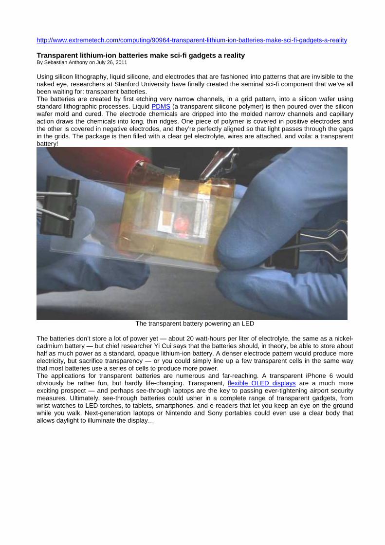
Using silicon lithography, liquid silicone, and electrodes that are fashioned into patterns that are invisible to thenaked eye, researchers at Stanford University have finally created the seminal sci-fi component that we’ve allbeen waiting for: transparent batteries.The batteries are created by first etching very narrow channels, in a grid pattern, into a silicon wafer usingstandard lithographic processes. Liquid PDMS (a transparent silicone polymer) is then poured over the siliconwafer mold and cured. The electrode chemicals are dripped into the molded narrow channels and capillaryaction draws the chemicals into long, thin ridges. One piece of polymer is covered in positive electrodes andthe other is covered in negative electrodes, and they’re perfectly aligned so that light passes through the gapsin the grids. The package is then filled with a clear gel electrolyte, wires are attached, and voila: a transparentbattery!
The transparent battery powering an LED
The batteries don’t store a lot of power yet — about 20 watt-hours per liter of electrolyte, the same as a nickel-cadmium battery — but chief researcher Yi Cui says that the batteries should, in theory, be able to store abouthalf as much power as a standard, opaque lithium-ion battery. A denser electrode pattern would produce moreelectricity, but sacrifice transparency — or you could simply line up a few transparent cells in the same waythat most batteries use a series of cells to produce more power.The applications for transparent batteries are numerous and far-reaching. A transparent iPhone 6 wouldobviously be rather fun, but hardly life-changing. Transparent, flexible OLED displays are a much moreexciting prospect — and perhaps see-through laptops are the key to passing ever-tightening airport securitymeasures. Ultimately, see-through batteries could usher in a complete range of transparent gadgets, fromwrist watches to LED torches, to tablets, smartphones, and e-readers that let you keep an eye on the groundwhile you walk. Next-generation laptops or Nintendo and Sony portables could even use a clear body thatallows daylight to illuminate the display…
Transparent & Flexible Electronics
14 Massimo Marrazzo - biodomotica.com
PPPPPPPPrrrrrrrriiiiiiiinnnnnnnntttttttteeeeeeeedddddddd EEEEEEEElllllllleeeeeeeeccccccccttttttttrrrrrrrroooooooonnnnnnnniiiiiiiiccccccccssssssss
- http://electronicsbus.com/ink-jet-printable-transparent-electronics-graphene-ink/
Ink-Jet Printable Transparent Electronics using Gra phene InkPosted by Karthikeya in Technology News
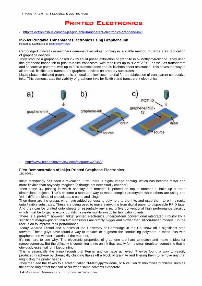
Cambridge University researchers demonstrated ink-jet printing as a viable method for large area fabricationof graphene devices.They produce a graphene-based ink by liquid phase exfoliation of graphite in N-Methylpyrrolidone. They usedthis graphene-based ink to print thin-film transistors, with mobilities up to 95cm2V−1s−1, as well as transparentand conductive patterns, with up to 80% transmittance and 30 kilohms sheet resistance. This paves the way toall-printed, flexible and transparent graphene devices on arbitrary substrates.Liquid phase exfoliated graphene is an ideal and low cost material for the fabrication of transparent conductiveinks. This demonstrates the viability of graphene-inks for flexible and transparent electronics.
- http://www.technologyreview.com/blog/arxiv/27368/
First Demonstration of Inkjet-Printed Graphene Elec tronics11/24/2011
Inkjet technology has been a revolution. First, there is digital image printing, which has become faster andmore flexible than anybody imagined (although not necessarily cheaper).Then came 3D printing in which one layer of material is printed on top of another to build up a threedimensional objects. That's become a standard way to make complex prototypes while others are using it to'print' different kinds of chocolates, creams and icings.Then there are the groups who have added conducting polymers to the inks and used them to print circuitsonto flexible substrates. These are being used to make everything from digital paper to disposable RFID tags.And they can be printed onto sheets of essentially any size, unlike conventional high performance circuitrywhich must be forged in exotic conditions inside multibillion dollar fabrication plants .There is a problem however. Inkjet printed electronics underperform conventional integrated circuitry by asignificant margin--printed thin film transistors are simply bigger and slower than silicon-based models. So therace is on to improve their performance.Today, Andrea Ferrari and buddies at the University of Cambridge in the UK show off a significant stepforward. These guys have found a way to replace or augment the conducting polymers in these inks withgraphene, the wonder-material of the moment.It's not hard to see why. The electronic properties of graphene are hard to match and make it idea fornanoelectronics. But the difficulty is combining it into an ink that readily forms small droplets--something that isobviously essential for inkjet printing.This is essentially the breakthrough that Ferrari and co have achieved. They've found a way to readilyproduced graphene by chemically chipping flakes off a block of graphite and filtering them to remove any thatmight clog the printer heads.They then add the flakes to a solvent called N-Methylpyrrolidone, or NMP, which minimises problems such asthe coffee ring effect that can occur when some solvents evaporate.
Finally they've put this stuff in their printers and printed out a few circuits and thin film transisters.The results are promising. The graphene-based inks match or beat the performance of most other inksavailable today. That's pretty good for a first attempt since improvements will certainly follow."This paves the way to all-printed, flexible and transparent graphene devices on arbitrary substrates.," sayFerrari and co in concluding their paper. Which means we can expect to see much more on this in the comingmonths and years.Ref: arxiv.org/abs/1111.4970: Ink-Jet Printed Graphene ElectronicsInk-Jet Printed Graphene ElectronicsF. Torrisi, T. Hasan, W. Wu, Z. Sun, A. Lombardo, T. Kulmala, G. W. Hshieh, S. J. Jung, F. Bonaccorso, P. J. Paul, D. P. Chu, A. C.Ferrari
- http://www.kurzweilai.net/graphene-based-inkjet-printing-allows-for-faster-flexible-electronics
Graphene-based inkjet printing allows for faster fl exible electronicsNovember 28, 2011 by Editor
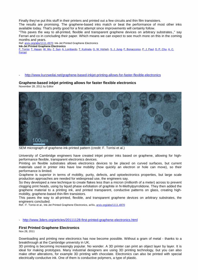
SEM micrograph of graphene-ink-printed pattern (credit: F. Torrisi et al.)
University of Cambridge engineers have created inkjet printer inks based on graphene, allowing for high-performance flexible, transparent electronics devices.Printing on flexible substrates allows electronics devices to be placed on curved surfaces, but currentmaterials used in printer inks have low mobility (how quickly an electron or hole can move), so theirperformance is limited.Graphene is superior in terms of mobility, purity, defects, and optoelectronics properties, but large scaleproduction approaches are needed for widespread use, the engineers say.So they developed a new technique to create flakes less than a micron (millionth of a meter) across to preventclogging print heads, using by liquid phase exfoliation of graphite in N-Methylpyrrolidone. They then added thegraphene material to a printing ink, and printed transparent, conductive patterns on glass, creating high-mobility, graphene-based thin-film transistors.This paves the way to all-printed, flexible, and transparent graphene devices on arbitrary substrates, theengineers concluded.Ref.: F. Torrisi et al., Ink-Jet Printed Graphene Electronics, arXiv, arxiv.org/abs/1111.4970
- http://www.3ders.org/articles/20111128-first-printed-graphene-electronics.html
First Printed Graphene ElectronicsNov.28, 2011
Downloading and printing new electronics has now become possible. Without a gram of metal - thanks to abreakthrough at the Cambridge university in UK.3D printing is becoming increasingly popular. No wonder. A 3D printer can print an object layer by layer. It isideal for making prototypes. Many industrial designers are using 3D printing technology, but you can alsomake other alterations, for example 3D printing with chocolate. Electronics can also be printed with specialelectrically conductive ink. One of them is conductive polymers, a type of plastic.
Transparent & Flexible Electronics
16 Massimo Marrazzo - biodomotica.com
There's only one problem. Printed electronics is far not as good as silicon-based electronics, because thematerial is less conductive. That is, until now, Andrea Ferrari and his colleagues at Cambridge have for thefirst time succeeded in graphene to replace conducting polymers. Graphene, which is a sort of chicken wiremade of carbon atoms in graphite, conducts as good as metals. In short, it is an ideal material for printableelectronics. Unfortunately it is very difficult to make a form by a printer head because of the graphene flakes.Graphene is an irregular mixture of small and large flakes. Large flakes clog the printer head and even biggerproblem can occur - it prevents the small, regular droplets to be formed. Small droplets are fundamental forinkjet printing.Recently, Andrea Ferrari and peers at the University of Cambridge in the UK have managed to solve thisproblem and demonstrated a giant leap forward. By using a modified Epson Stylus 1500 Ink-jet printer andsome customised cartridges, they have printed out onto a Silicon based substrate.
They peel graphene layers off with ultrasound (in jargon: sonication) from a graphite block and filter them sothat the largest pieces are no longer clogging the printer head. Then they solve the flakes in the solvent N-methylpyrrolidone, or NMP, which counteracts the infamous coffee ring effect(In physics, a coffee ring is apattern left by a puddle of particle-laden liquid after it evaporates). The ink is accumulated on the edge by thiscoffee ring effect. Another nice feature is that NMP is not very toxic. The last step was to place the NMP withdissolved grafeenvlokken in a printhead. The researchers printed a number of circuits and thin film transistors.The breakthrough shows the graphene ink scoring slightly better than existing ink. Note: this is not a matureproduct, so expect that it will be even better."This paves the way to all-printed, flexible and transparent graphene devices on arbitrary substrates.," sayFerrari and co in concluding their paper.If this technology is combined with 3D printing technology, soon you will be in a printing service shop askingfor printing a 3D objects with internal electronics.
- http://news.illinois.edu/news/11/0628silver_pen_JenniferLewis.html
Silver pen has the write stuff for flexible electro nics
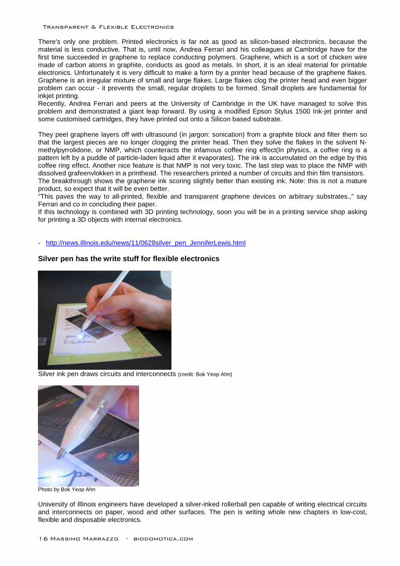
Silver ink pen draws circuits and interconnects (credit: Bok Yeop Ahn)
Photo by Bok Yeop Ahn
University of Illinois engineers have developed a silver-inked rollerball pen capable of writing electrical circuitsand interconnects on paper, wood and other surfaces. The pen is writing whole new chapters in low-cost,flexible and disposable electronics.
Led by Jennifer Lewis, the Hans Thurnauer professor of materials science and engineering at the U. of I., andJennifer Bernhard, a professor of electrical and computer engineering, the team published its work in thejournal Advanced Materials.
“Pen-based printing allows one to construct electronic devices ‘on-the-fly,’ ” said Lewis, the director of theFrederick Seitz Materials Research Laboratory at the U. of I. “This is an important step toward enablingdesktop manufacturing (or personal fabrication) using very low cost, ubiquitous printing tools.”
While it looks like a typical silver-colored rollerball pen, this pen’s ink is a solution of real silver. After writing,the liquid in the ink dries to leave conductive silver pathways – in essence, paper-mounted wires. The inkmaintains its conductivity through multiple bends and folds of the paper, enabling devices with great flexibilityand conformability.Metallic inks have been used in approaches using inkjet printers to fabricate electronic devices, but the penoffers freedom and flexibility to apply ink directly to paper or other rough surfaces instantly, at low cost andwithout programming.
“The key advantage of the pen is that the costly printers and printheads typically required for inkjet or otherprinting approaches are replaced with an inexpensive, hand-held writing tool,” said Lewis, who is also affiliatedwith the Beckman Institute for Advanced Science and Technology.
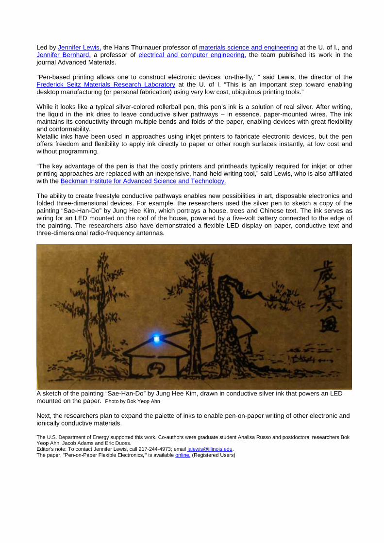
The ability to create freestyle conductive pathways enables new possibilities in art, disposable electronics andfolded three-dimensional devices. For example, the researchers used the silver pen to sketch a copy of thepainting “Sae-Han-Do” by Jung Hee Kim, which portrays a house, trees and Chinese text. The ink serves aswiring for an LED mounted on the roof of the house, powered by a five-volt battery connected to the edge ofthe painting. The researchers also have demonstrated a flexible LED display on paper, conductive text andthree-dimensional radio-frequency antennas.
A sketch of the painting “Sae-Han-Do” by Jung Hee Kim, drawn in conductive silver ink that powers an LEDmounted on the paper. Photo by Bok Yeop Ahn
Next, the researchers plan to expand the palette of inks to enable pen-on-paper writing of other electronic andionically conductive materials.
The U.S. Department of Energy supported this work. Co-authors were graduate student Analisa Russo and postdoctoral researchers BokYeop Ahn, Jacob Adams and Eric Duoss.Editor's note: To contact Jennifer Lewis, call 217-244-4973; email [email protected] paper, “Pen-on-Paper Flexible Electronics,” is available online. (Registered Users)
Transparent & Flexible Electronics
18 Massimo Marrazzo - biodomotica.com
eeeeeeee--------PPPPPPPPaaaaaaaappppppppeeeeeeeerrrrrrrr
- http://www.netbooknews.com/32821/colourful-flexible-rewritable-epaper-prototype-demo/
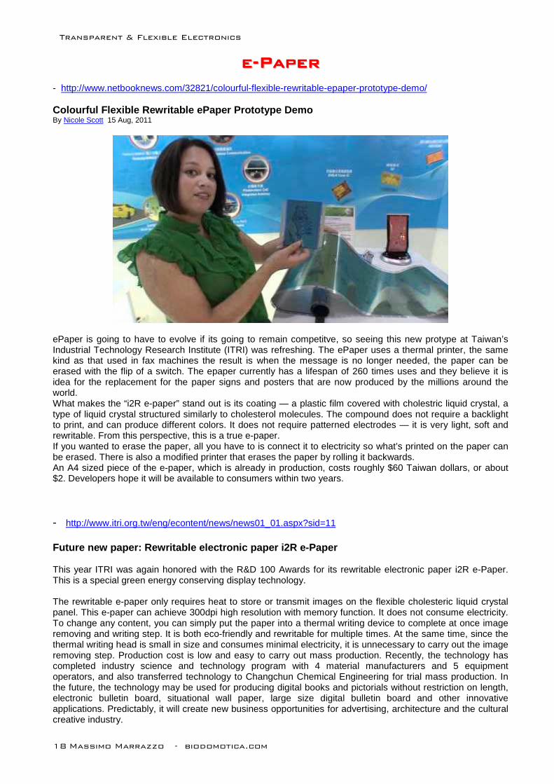
Colourful Flexible Rewritable ePaper Prototype DemoBy Nicole Scott 15 Aug, 2011
ePaper is going to have to evolve if its going to remain competitve, so seeing this new protype at Taiwan’sIndustrial Technology Research Institute (ITRI) was refreshing. The ePaper uses a thermal printer, the samekind as that used in fax machines the result is when the message is no longer needed, the paper can beerased with the flip of a switch. The epaper currently has a lifespan of 260 times uses and they believe it isidea for the replacement for the paper signs and posters that are now produced by the millions around theworld.What makes the “i2R e-paper” stand out is its coating — a plastic film covered with cholestric liquid crystal, atype of liquid crystal structured similarly to cholesterol molecules. The compound does not require a backlightto print, and can produce different colors. It does not require patterned electrodes — it is very light, soft andrewritable. From this perspective, this is a true e-paper.If you wanted to erase the paper, all you have to is connect it to electricity so what’s printed on the paper canbe erased. There is also a modified printer that erases the paper by rolling it backwards.An A4 sized piece of the e-paper, which is already in production, costs roughly $60 Taiwan dollars, or about$2. Developers hope it will be available to consumers within two years.
- http://www.itri.org.tw/eng/econtent/news/news01_01.aspx?sid=11
Future new paper: Rewritable electronic paper i2R e -Paper
This year ITRI was again honored with the R&D 100 Awards for its rewritable electronic paper i2R e-Paper.This is a special green energy conserving display technology.
The rewritable e-paper only requires heat to store or transmit images on the flexible cholesteric liquid crystalpanel. This e-paper can achieve 300dpi high resolution with memory function. It does not consume electricity.To change any content, you can simply put the paper into a thermal writing device to complete at once imageremoving and writing step. It is both eco-friendly and rewritable for multiple times. At the same time, since thethermal writing head is small in size and consumes minimal electricity, it is unnecessary to carry out the imageremoving step. Production cost is low and easy to carry out mass production. Recently, the technology hascompleted industry science and technology program with 4 material manufacturers and 5 equipmentoperators, and also transferred technology to Changchun Chemical Engineering for trial mass production. Inthe future, the technology may be used for producing digital books and pictorials without restriction on length,electronic bulletin board, situational wall paper, large size digital bulletin board and other innovativeapplications. Predictably, it will create new business opportunities for advertising, architecture and the culturalcreative industry.
- http://www.plusplasticelectronics.com/publishingmedia/itri-unveils-rewritable-e-paper-36686.aspx
ITRI unveils rewritable e-paperSara Ver-Bruggen - 08 Aug 2011
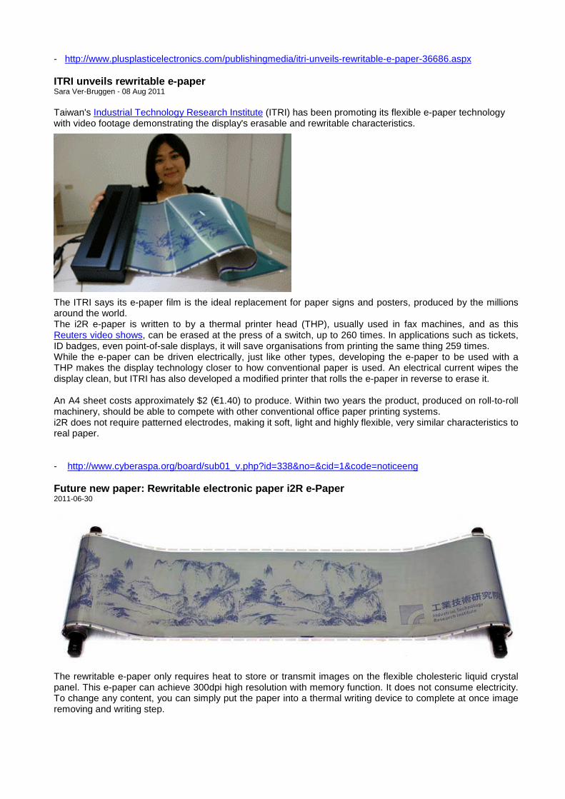
Taiwan's Industrial Technology Research Institute (ITRI) has been promoting its flexible e-paper technologywith video footage demonstrating the display's erasable and rewritable characteristics.
The ITRI says its e-paper film is the ideal replacement for paper signs and posters, produced by the millionsaround the world.The i2R e-paper is written to by a thermal printer head (THP), usually used in fax machines, and as thisReuters video shows, can be erased at the press of a switch, up to 260 times. In applications such as tickets,ID badges, even point-of-sale displays, it will save organisations from printing the same thing 259 times.While the e-paper can be driven electrically, just like other types, developing the e-paper to be used with aTHP makes the display technology closer to how conventional paper is used. An electrical current wipes thedisplay clean, but ITRI has also developed a modified printer that rolls the e-paper in reverse to erase it.
An A4 sheet costs approximately $2 (€1.40) to produce. Within two years the product, produced on roll-to-rollmachinery, should be able to compete with other conventional office paper printing systems.i2R does not require patterned electrodes, making it soft, light and highly flexible, very similar characteristics toreal paper.
- http://www.cyberaspa.org/board/sub01_v.php?id=338&no=&cid=1&code=noticeeng
Future new paper: Rewritable electronic paper i2R e -Paper2011-06-30
The rewritable e-paper only requires heat to store or transmit images on the flexible cholesteric liquid crystalpanel. This e-paper can achieve 300dpi high resolution with memory function. It does not consume electricity.To change any content, you can simply put the paper into a thermal writing device to complete at once imageremoving and writing step.
Transparent & Flexible Electronics
20 Massimo Marrazzo - biodomotica.com
- http://www.hml.queensu.ca/paperphone
Revolutionary new paper computer shows flexible fut ure for smartphones and tabletsQueen’s University’s Roel Vertegaal says thinfilm phone will make current smartphone obsolete in 5 to 10years.May 5, 2011
KINGSTON, ONTARIO – The world’s first interactive paper computer is set to revolutionize the world ofinteractive computing.
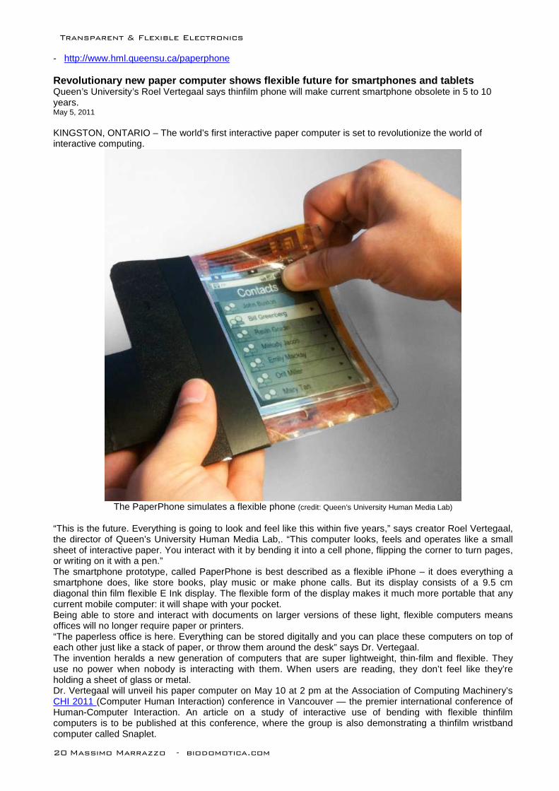
The PaperPhone simulates a flexible phone (credit: Queen’s University Human Media Lab)
“This is the future. Everything is going to look and feel like this within five years,” says creator Roel Vertegaal,the director of Queen’s University Human Media Lab,. “This computer looks, feels and operates like a smallsheet of interactive paper. You interact with it by bending it into a cell phone, flipping the corner to turn pages,or writing on it with a pen.”The smartphone prototype, called PaperPhone is best described as a flexible iPhone – it does everything asmartphone does, like store books, play music or make phone calls. But its display consists of a 9.5 cmdiagonal thin film flexible E Ink display. The flexible form of the display makes it much more portable that anycurrent mobile computer: it will shape with your pocket.Being able to store and interact with documents on larger versions of these light, flexible computers meansoffices will no longer require paper or printers.“The paperless office is here. Everything can be stored digitally and you can place these computers on top ofeach other just like a stack of paper, or throw them around the desk” says Dr. Vertegaal.The invention heralds a new generation of computers that are super lightweight, thin-film and flexible. Theyuse no power when nobody is interacting with them. When users are reading, they don’t feel like they’reholding a sheet of glass or metal.Dr. Vertegaal will unveil his paper computer on May 10 at 2 pm at the Association of Computing Machinery’sCHI 2011 (Computer Human Interaction) conference in Vancouver — the premier international conference ofHuman-Computer Interaction. An article on a study of interactive use of bending with flexible thinfilmcomputers is to be published at this conference, where the group is also demonstrating a thinfilm wristbandcomputer called Snaplet.

The development team included researchers Byron Lahey and Win Burleson of the Motivational EnvironmentsResearch Group at Arizona State University (ASU), Audrey Girouard and Aneesh Tarun from the HumanMedia Lab at Queen’s University, Jann Kaminski and Nick Colaneri, director of ASU’s Flexible Display Center,and Seth Bishop and Michael McCreary, the VP R&D of E Ink Corporation.
Video – PaperPhone demonstrationVideo – Snaplet wristband computerArticles and High Resolution Photos – See attachments.To arrange an interview or for a copy of the papers, please contact Michael Onesi at (613)533-6000 ext [email protected], News and Media Services, Queen’s University.
Attachment SizePaperPhone ACM CHI 2011 Scientific Article 5.19 MBSnaplet ACM CHI 2011 Scientific Article 1.85 MBPaperPhone Hi-Res Image (JPG) 1.15 MBSnaplet Hi-Res Image 1 (JPG) 1.51 MBSnaplet Hi-Res Image 2 (JPG) 2.93 MBPaperPhone Hi-Res Video (mp4) 27.68 MBSnaplet Hi-Res Video (mp4) 6.24 MB
Transparent & Flexible Electronics
22 Massimo Marrazzo - biodomotica.com
PPPPPPPPllllllllaaaaaaaassssssssttttttttiiiiiiiicccccccc EEEEEEEElllllllleeeeeeeeccccccccttttttttrrrrrrrroooooooonnnnnnnniiiiiiiiccccccccssssssss
- http://www.plusplasticelectronics.com/what-are-plastic-electronics.aspx
What are plastic electronics?
Plastic electronics encompasses a number of technologies and terms, some of which can be confusing.However, when you know what individual terms mean, the entire market starts to make more sense.
AMOLED - stands for Active Matrix Organic Light Emitting Diode, and is a form of display on televisions,smartphones and tablets. A number of companies have launched products using AMOLED screens over thecourse of the last 12 months.Backplane - the portion of a display that controls the pixels located in the frontplane.Barrier film - a flexible transparent film to cover materials involved in organic electronics, protecting them fromexposure to oxygen and water vapour, allowing them to remain non-rigid and extending their life spanconsiderably. Developments in barrier film technology are making it more instrumental for plastic electronicsproductsBuilding-integrated photovoltaics - solar cells integrated into a building design, with the intention ofsupplying power. Quite often these are made up of thin-film or transparent solar cells that cover a large area.Areas exploited for solar cell integration include windows, glass facades and roofs; and some solar cells arebeing developed for indoor use.{PRIVATE "TYPE=PICT;ALT=Carbon nanotubes are strong and conductive, and able to be used in areassuch as ITO alternatives"}Carbon nanotubes - molecular-scale tubes of graphite carbon, with strongelectronic properties. They can be metallic or semiconducting depending on their structure, making somemore conductive than copper, and others react similar to silicone. This could lead to nanoscale electronicdevices.Carbon nanotubes have been developed to replace indium tin oxide, a standard material in touchscreens forconsumer electronics devices.Colour rendering index - the index by which a light source is measured on how accurately it can reproduceall frequencies of the colour spectrum. The lower the CRI, the less accurate its colours are.Conductive ink - ink that is able to conduct electricity: it can be printed on a number of materials includingpaper and fabrics. It allows for more scope than etching out conventional circuit boards. Recently, companieshave invested in the production of graphene based conductive inks, which can be used in retail packaging.Dye-sensitised solar cell - a form of thin-film solar cell. Rather than thick silicon plates, a molecular dye,which absorbs sunlight, is places on a thin film beneath a transparent electrode, used to capture the energyproduced.The technology, which mimics the photosynthesis process in plants, can absorb much lower levels of lightthan conventional solar cell technology, making it suitable for indoor light or cloudy conditions.Electrochromic - substances that change colour or transparency when an electrical charge is applied, suchas LCD displays.{PRIVATE "TYPE=PICT;ALT=Shelf labels using e-paper can be quickly updated"}Electronic shelf label - athin display used by retailers to advertise the prices of products on shelves. Thin enough to sit in front of theproducts, they allow quick price amendments without the waste of paper. Electronic shelf labels have beendesigned in both LCD and e-paper formats.Electrowetting - the process whereby the surface tension of a liquid on a solid surface can be modified byapplying a voltage. The technology opens the possibility of low-power, colour and video-rate displays,according to developers like Liquavista and Gamma Dynamics.E-paper - a display which mimics the effects of paper, reflecting light rather than being backlit, and is able tohold images without electronic stimulation until required.Applications include e-readers, such as the Amazon Kindle, electronic shelf labels and other signage.E-reader - a portable device mainly used for reading books or documents, using e-paper technology. Notablee-reader products include the Amazon Kindle and{PRIVATE "TYPE=PICT;ALT=Flexible products are in development, but still some way off being marketable"}Flexible electronics - the mounting of electronics onto flexible materials, such as plastics or conductivepolyester. They are often printed, and are usually low cost, easier to produce and much thinner thanconventional circuits, allowing for a wider range of applications.Frontplane - The display of an electronic device, which can be made up of various elements.
Graphene - A thin yet strong material with excellent conductive properties. Formed from carbon atoms,graphene is more conductive than copper, and mixed into plastics, can turn them into strong semiconductors.Countries such as the UK are investing in graphene as its importance in plastic electronics increases.Heterojunction - A junction between two semiconductors, they are often used in organic photovoltaics totransfer energy.Hybrid electronics - a device or circuit that incorporates both organic and inorganic elementsIndium tin oxide - a transparent conducting coating used for many displays, such as flat screen televisionsand OLED applications, and solar cells. It is not flexible, and is used in mainly rigid products. Concerns oversupply and cost mean a number of companies are developing alternatives to ITO, such as PEDOT and carbonnanotube layers.Inkjet - a printer which places droplets of ink onto a subject. It can be used with conductive ink to produceprinted electronics, and is more precise in doing so.{PRIVATE "TYPE=PICT;ALT=Smart buildings are able to control light levels"}Integrated smart systems - Aseries of sensors and other electronics which are integrated into systems allowing them to functionindependently. One example may be a house, which is able to sense temperature and alter sunlight levels orcontrol air conditioning.Large-area electronics - Often manufactured using roll-to-roll techniques, large-area electronics are plasticelectronics products printed on large substrates with the ability to cover more area, such as organicphotovoltaics. Funding competitions have recently been announced to encourage collaboration on thedevelopment of large-area electronics.Lumens per watt - The measurement of light output per electricity used, measured in watts. The higher theLumens, and lower the wattage, the more efficient the product.Nanoink - ink, formed of nanoparticles, which is able to conduct electricity. As an ink, it can be printed ontothin film, or paper, allowing it to conduct current.Nanoparticles - particles with the dimensions of 100nm or less, extremely small, and able to be used with thinelectronic circuits.OLED display - a display made up of organic light emitting diodes, which emit light under electrical response.As they do not need a backlight, products using this display can be made thinner, and more flexible. OLEDdisplays are already used in smartphones and are expected to increase in popularity with use in televisionsduring 2012OLED light - a thin or flexible light panel, made of a single-colour OLED display.Organic semiconductor - a carbon-based semiconductor, where the flow of electrons is regulated by theproperties of the material used.{PRIVATE "TYPE=PICT;ALT=Organic solar cells can be produced in large areas"}Organic solar cell - a solarcell, which can absorb light and produce electricity, printed using organic material, such as polymersubstrates.PEDOT - a polymer-based material used in the production of printed organic electronics, especially organicsolar cells. The conductive layer material is considered a potential replacement for indium tin oxide. It couldopen a new avenue for nanoelectronic devices.Photonics - the transmission, signal processing, amplification, detection and sensing of light. Comprisingtechnologies such as LEDs, wireless sensor networks and solar cells, it is becoming increasingly convergentwith organic electronicsPMOLED - Passive Matrix OLEDs are smaller than other OLEDs, are controlled in rows and columns, ratherthan by each individual pixel.Printed battery - An energy storage device which is printed onto a flexible substrate, printed batteries areused to make a flexible electronic product remain so, with no rigid parts. They are often printed on paper.Printed diagnostic devices / biosensor - electronic devices used in the detecting or sensing of medicalconditions. Using printed electronic concepts, developers are working on cheap, disposable versions of thesedevices.Printed electronics - an electronic circuit or device that is printed onto a substrate, rather than etched. Theycan be flexible, and thin, to aid the design of the products using them.{PRIVATE "TYPE=PICT;ALT=RFID tags are printed on a number of substrates including paper"}QLED - aquantum dot LED, which is thinner than OLEDs, and is able to emit a brighter range of colours. This allows forthinner, more visible and more flexible displays.Quantum dots - a small particle of semiconductor material, which is able to be tuned to emit light of differingcolours. They can also be used to capture light and convert it to energy in organic photovoltaics.RFID - Radio Frequency ID is a method of transmitting data to a reader via radio frequencies. It can allow forproducts to be given unique ID codes, which can be easily scanned for information to appear. They do notneed to be visible to be read. RFID technology has a number of potential uses, including healthcare.Roll-to-roll - the process of creating flexible electronics, often meaning being printed on a roll of film, orplastic.Smart packaging - product packaging with integrated electronics that is able to give a range of information,from transmitting ID codes, to informing doctors when a patient takes their pills. Animated logos and sensors
Transparent & Flexible Electronics
24 Massimo Marrazzo - biodomotica.com
for brand protection are also being designed. A number of companies are already pushing forward with pilotproducts.Smart textiles and fabrics - a material with integrated electronic properties. This could be printed on to beused in electronic devices, like fibres, or actual clothing with sensors embedded to allow monitoring of variousconditions. Smart textiles are also becoming increasingly common in fashion.Spin coating - a process used to apply thin-film coating to substrates, where an excess layer of fluid isapplied, and then the substrate is spun at high speed to spread the fluid thinly over the surface.Spray coating - a process to apply flexible electronics to substrates, using a spray on technique which can bedone at room temperature.{PRIVATE "TYPE=PICT;ALT=Smart fabrics are becoming more widespread in fashion design"}Thin-film - alayer of film, often around a nanometre thick. Used in roll-to-roll processes for electronic semiconductorproduction due to its cost.Thin-film transistor - a transformer used in high-matrix LCD displays to control the individual sub-pixels.Vacuum deposition - the process of depositing thin layers onto a substrate, such as a thin film. It is usuallydone in a vacuum.Wearable electronics - electronic devices that are woven into fabrics, clothing and other material products.These could be monitors to measure various athletic or medical traits, such as heartbeat, perspiration ormuscle control. They can also be used for novalty items or to act as chargers for mobile devices.
…………………………………………………………………………………………………………
…………………………………………………………………………………………………………
…………………………………………………………………………………………………………
…………………………………………………………………………………………………………
…………………………………………………………………………………………………………
…………………………………………………………………………………………………………
…………………………………………………………………………………………………………
…………………………………………………………………………………………………………
…………………………………………………………………………………………………………
…………………………………………………………………………………………………………
…………………………………………………………………………………………………………
…………………………………………………………………………………………………………
…………………………………………………………………………………………………………
…………………………………………………………………………………………………………
…………………………………………………………………………………………………………
…………………………………………………………………………………………………………
…………………………………………………………………………………………………………
…………………………………………………………………………………………………………
…………………………………………………………………………………………………………
…………………………………………………………………………………………………………
…………………………………………………………………………………………………………
…………………………………………………………………………………………………………
…………………………………………………………………………………………………………
…………………………………………………………………………………………………………
…………………………………………………………………………………………………………

…………………………………………………………………………………………………………
…………………………………………………………………………………………………………
…………………………………………………………………………………………………………
…………………………………………………………………………………………………………
…………………………………………………………………………………………………………
Transparent & Flexible Electronics
26 Massimo Marrazzo - biodomotica.com
LLLLLLLLiiiiiiiinnnnnnnnkkkkkkkkssssssss
http://www.plusplasticelectronics.com/Independent Analysis for Organic and Printable ElectronicsPlusplasticelectronics.com provides timely news and analysis, researched and written by business andtechnology editors and supported by independent experts, to help companies plan their strategies in thisemerging, dynamic marketplace.
http://nextbigfuture.com/Coverage of Science and Technology having high potential for disruption & Analysis of plans, policies and technology toenable radical improvements.
http://www.physorg.com/nanotech-news/PhysOrg.com™ is a leading web-based science, research and technology news service which covers a fullrange of topics. These include physics, earth science, medicine, nanotechnology, electronics, space, biology,chemistry, computer sciences, engineering, mathematics and other sciences and technologies
http://www.innovationnewsdaily.com/InnovationNewsDaily reports on futuristic technologies, innovations, disruptive ideas and cool gadgets that willshape the future, and explain why it all matters and how it will affect your life.
http://www.extremetech.com/We’re a thriving community of users and experts seeking to answer the unanswerable questions oftechnology. We dig deep into the subterranean depths of technological knowledge, digging up the most vital,behind-the-scenes tidbits that make any technocrats drool soda on his chips
http://electronicsbus.com/ELECTRONICSBUS Magazine is an International Media, provides an interactive platform for every electronicsengineer, from beginners to experts. This magazine provides information, education, inspiration andentertainment. News & Views from Electronics manufacturers and research organizations.
http://www.technologyreview.com/Technology Review is an independent media company owned by the Massachusetts Institute of Technology(MIT). Technology Review identifies emerging technologies and analyzes their impact for technology andbusiness leaders—the senior executives, entrepreneurs, venture capitalists, engineers, developers, andresearchers who create and fund the innovations that drive the global economy.
http://www.kurzweilai.net/KurzweilAI explores the forecasts and insights on accelerating change articulated in Ray Kurzweil’s landmarkbooks — notably The Age of Spiritual Machines and The Singularity Is Near — and updates these books withkey breakthroughs in science and technology.
http://www.3ders.org/index.html3ders.org focus on 3D printing field and brings "entertaining but useful news in 3D printing".
http://www.cyberaspa.org/ASPA is an international nongovernmental organization established in Japan in 1997 for the purpose ofaccomplishing the joint development in the fields of scientific technology, industry and economy in the Asianregion.

SSSSSSSShhhhhhhhoooooooowwwwwwww////////CCCCCCCCoooooooonnnnnnnnvvvvvvvveeeeeeeennnnnnnnttttttttiiiiiiiioooooooonnnnnnnn////////EEEEEEEExxxxxxxxppppppppoooooooossssssssiiiiiiiittttttttiiiiiiiioooooooonnnnnnnn
OLEDs, Smart Fabrics, OPVs, Nanomaterials conferenc e and events 2012 –
+Plastic Electronicshttp://www.plusplasticelectronics.com/EventDiary2012.aspx
Transparent & Flexible Electronics
28 Massimo Marrazzo - biodomotica.com
22222222000000001111111122222222 UUUUUUUUppppppppddddddddaaaaaaaatttttttteeeeeeee
…………………………………………………………………………………………………………
…………………………………………………………………………………………………………
…………………………………………………………………………………………………………
…………………………………………………………………………………………………………
…………………………………………………………………………………………………………
…………………………………………………………………………………………………………
…………………………………………………………………………………………………………
…………………………………………………………………………………………………………
…………………………………………………………………………………………………………
…………………………………………………………………………………………………………
…………………………………………………………………………………………………………
…………………………………………………………………………………………………………
…………………………………………………………………………………………………………
…………………………………………………………………………………………………………
…………………………………………………………………………………………………………
…………………………………………………………………………………………………………
…………………………………………………………………………………………………………
…………………………………………………………………………………………………………
…………………………………………………………………………………………………………
…………………………………………………………………………………………………………
…………………………………………………………………………………………………………
…………………………………………………………………………………………………………
…………………………………………………………………………………………………………
…………………………………………………………………………………………………………
…………………………………………………………………………………………………………
…………………………………………………………………………………………………………
…………………………………………………………………………………………………………
…………………………………………………………………………………………………………
…………………………………………………………………………………………………………
…………………………………………………………………………………………………………
BIODOMOTICABIODOMOTICABIODOMOTICABIODOMOTICA
Massimo Marrazzowww.biodomotica.com [email protected]
DisclaimerNo one can sell or ask money for this e-book.
Every info in this document is available free on Internet, like this e-book.I don’t receive money or any other benefits by the companies cited.
I’m not responsible for errors, damages, mistakes o any fraud by websites listed in this e-book.If you don’t want be mentioned here just write me an email to ([email protected])
and I’ll delete any reference of you from this e-book.
Copyright © 2012 Massimo Marrazzo - BiodomoticaThis document may be used and distributed provided that this copyright statement is not removed
from the file and that any derivative work contains the original copyright notice.If you want reproduce, distribute, print articles mentioned in this e-book
you must contact owners of copyright, not me.
Any of the trademarks, service marks, collective marks, design rights or similar rights that are mentioned,used or cited in “A foldable World” are the property of their respective owners.
See also Nanotechnology vol.1 Transparent & Flexible electronicswww.biodomotica.com/public/foldable_world.pdf
See also: Nanotechnology vol.2 Technology for E-books Readers (B/W & colors display)www.biodomotica.com/public/e-paper_e-book.pdf