fault tree analysis (fta) - ti.com · current limit detection failure fault tree . slva555 . 16....
TRANSCRIPT
Application Report SLVA555 –December 2012
1
Fault Tree Analysis (FTA) Samir Camdzic Automotive Products
ABSTRACT
ASIC level FTA used in automotive applications in cabin temperature environment. FTA analysis completed from perspective of fault(s) causing hazard regardless of time when fault(s) occur. This could be from time t = 0 onward.
Contents 1 References ....................................................................................................................................... 2 2 Diagrams .......................................................................................................................................... 3 3 Hazards .......................................................................................................................................... 26 4 Analysis ......................................................................................................................................... 26
4.1 Description .............................................................................................................................. 26 4.2 Faulty Switch Regulator Cut Sets ............................................................................................ 26
5 Conclusion ..................................................................................................................................... 26
Figures Figure 1. Device Block Diagram ........................................................................................................ 3 Figure 2. TPS54310-Q1 Undervoltage Fault Tree ............................................................................ 4 Figure 3. Faulty Regulation Fault Tree ............................................................................................. 5 Figure 4. Faulty Voltage Monitoring Fault Tree ............................................................................... 6 Figure 5. HS Pre-Driver Failure Fault Tree ....................................................................................... 7 Figure 6. Voltage Reference Failure Fault Tree ............................................................................... 8 Figure 7. OSC Frequency Setting Failure ........................................................................................ 9 Figure 8. LS Pre-Driver Failure Fault Tree ..................................................................................... 10 Figure 9. VIN Failure Fault Tree ...................................................................................................... 11 Figure 10. VSENSE Power Good Detection failure fault tree ......................................................... 12 Figure 11. Set/Reset Circuit Failure fault tree .................................................................................. 13 Figure 12. PWM Generation failure fault tree ................................................................................... 14 Figure 13. Current Limit Detection failure fault tree ....................................................................... 15 Figure 14. Shutdown Detection failure fault tree ............................................................................. 16 Figure 15. Slow Start failure fault tree .............................................................................................. 17 Figure 16. High Side Supply failure fault tree .................................................................................. 18 Figure 17. VIN Undervoltage Lockout failure fault tree .................................................................. 19 Figure 18. SS/ENA Detection failure fault tree ................................................................................. 20 Figure 19. Reference clock failure .................................................................................................... 21 Figure 20. SS/EN Comparator failure fault tree ............................................................................... 22 Figure 21. Internal Regulator failure fault tree ................................................................................. 23 Figure 22. TPS54310 Undervoltage fault tree importance diagram ............................................... 24 Figure 23. Faulty Regulation fault tree importance diagram .......................................................... 24 Figure 24. VSENSE Monitoring fault tree importance diagram ...................................................... 25 Figure 25. Adaptive PWM Control Circuit fault tree importance diagram ..................................... 25
SLVA555
2 Fault Tree Analysis (FTA)
ABBREVIATIONS
AMP Amplifier BG Bandgap BVDSS Drain Source Breakdown Voltage BW Bond Wire COMP Comparator EPB Electronic Park Brake IDDQ Quiescent Supply Current OVST Over Voltage Stress Test PT Production Test PTAT Proportional to Absolute Temperature REF Reference REG Regulator S/C Short Circuit SOA Safe Operating Area URA Unintended Relay Actuation V5AOV V5A Regulator Over Voltage V5OV V5 Regulator Over Voltage
1 References SLVS726 - 3-V TO 6-V INPUT, 6-A OUTPUT SYNCHRONOUS BUCK PWM SWITCHER WITH INTEGRATED FETs (SWIFT™) - January 2007 (http://www.ti.com/lit/gpn/tps54610-q1)
SLVA555
Fault Tree Analysis (FTA) 3
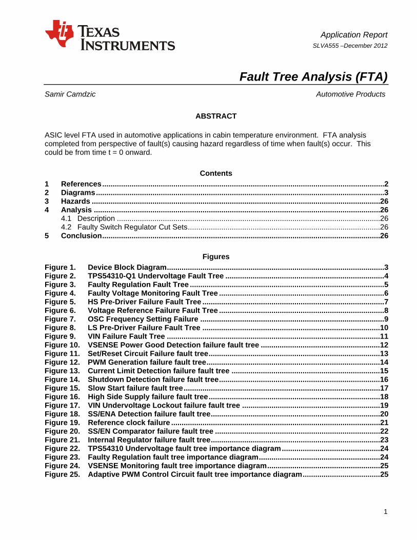
2 Diagrams
Figure 1. Device Block Diagram
SLVA555
4 Fault Tree Analysis (FTA)
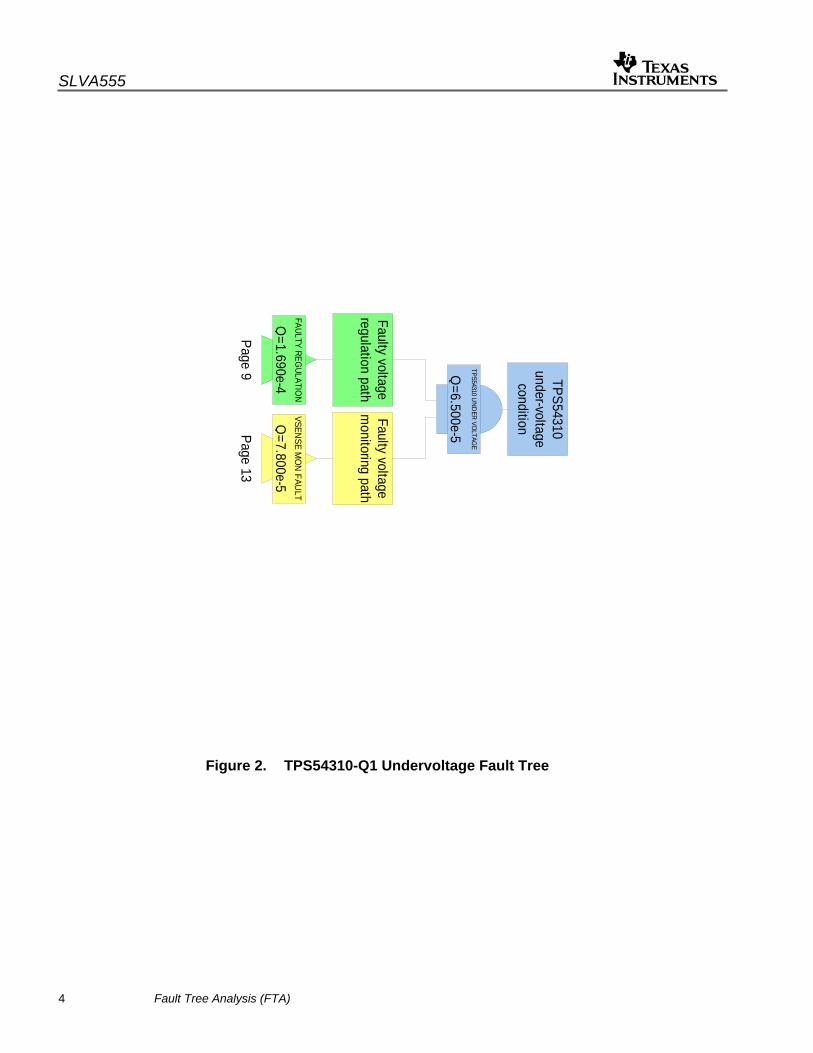
Figure 2. TPS54310-Q1 Undervoltage Fault Tree
TPS54310 UN
DER
VOLTAG
E
Q=6.500e-5
TPS54310under-voltage
condition
FAULTY REGULATIO
N
Q=1.690e-4
Faulty voltageregulation path
Page 9
VSENSE M
ON
FAULT
Q=7.800e-5
Faulty voltagem
onitoring path
Page 13
SLVA555
Fault Tree Analysis (FTA) 5
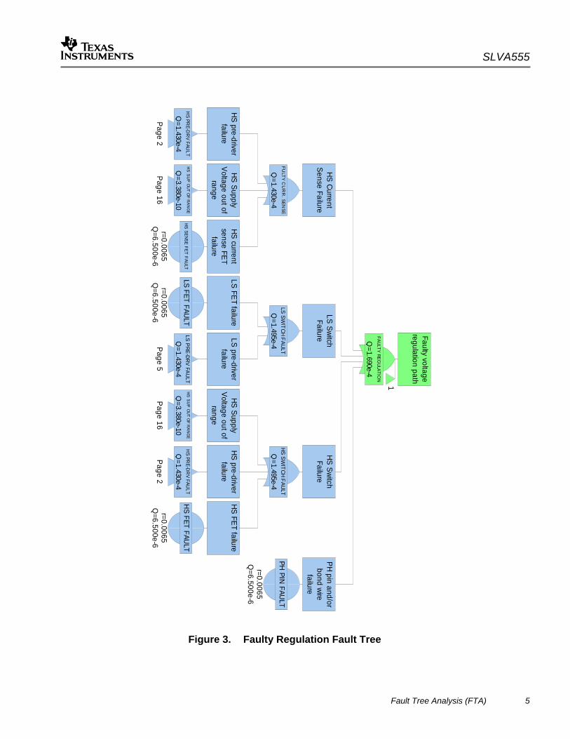
FAULTY REGULATIO
N
Q=1.690e-4
Faulty voltageregulation path
1
FULTY C
UR
R. SEN
SE
Q=1.430e-4
HS CurrentSense Failure
LS SWITCH FAULT
Q=1.495e-4
LS SwitchFailure
HS SWITCH FAULT
Q=1.495e-4
HS SwitchFailure
PH PIN
FAULT
PH pin and/orbond wire
failure
r=0.0065Q
=6.500e-6
HS PR
E-DR
V FAULT
Q=1.430e-4
HS pre-driverfailure
Page 2
HS SU
P OUT O
F RAN
GE
Q=3.380e-10
HS SupplyVoltage out of
range
Page 16
HS SENSE FET FAULT
HS currentsense FET
failure
r=0.0065Q
=6.500e-6
LS PRE-DRV FAULT
Q=1.430e-4
LS pre-driverfailure
Page 5
LS FET FAULT
LS FET failure
r=0.0065Q
=6.500e-6
HS SU
P OUT O
F RAN
GE
Q=3.380e-10
HS SupplyVoltage out of
range
Page 16
HS PR
E-DR
V FAULT
Q=1.430e-4
HS pre-driverfailure
Page 2
HS FET FAU
LT
HS FET failure
r=0.0065Q
=6.500e-6
Figure 3. Faulty Regulation Fault Tree
SLVA555
6 Fault Tree Analysis (FTA)
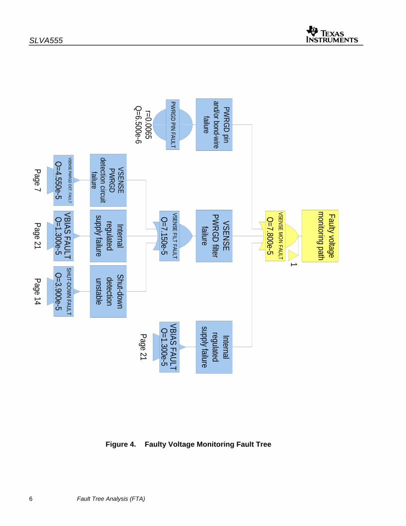
VSENSE MO
N FAULT
Q=7.800e-5
Faulty voltagem
onitoring path
1
VSENSE FILT FAULT
Q=7.150e-5
VSENSEPW
RGD filterfailure
VBIAS FAULTQ=1.300e-5
Internalregulated
supply failure
Page 21
PWRGD PIN FAULT
PWRGD pin
and/or bond-wirefailure
r=0.0065Q=6.500e-6
VSENSE PWRGD DET. FAULT
Q=4.550e-5
VSENSEPW
RGDdetection circuit
failure
Page 7
VBIAS FAULTQ=1.300e-5
Internalregulated
supply failure
Page 21
SHUT-DOW
N FAULT
Q=3.900e-5
Shut-downdetectionunstable
Page 14
Figure 4. Faulty Voltage Monitoring Fault Tree
SLVA555
Fault Tree Analysis (FTA) 7
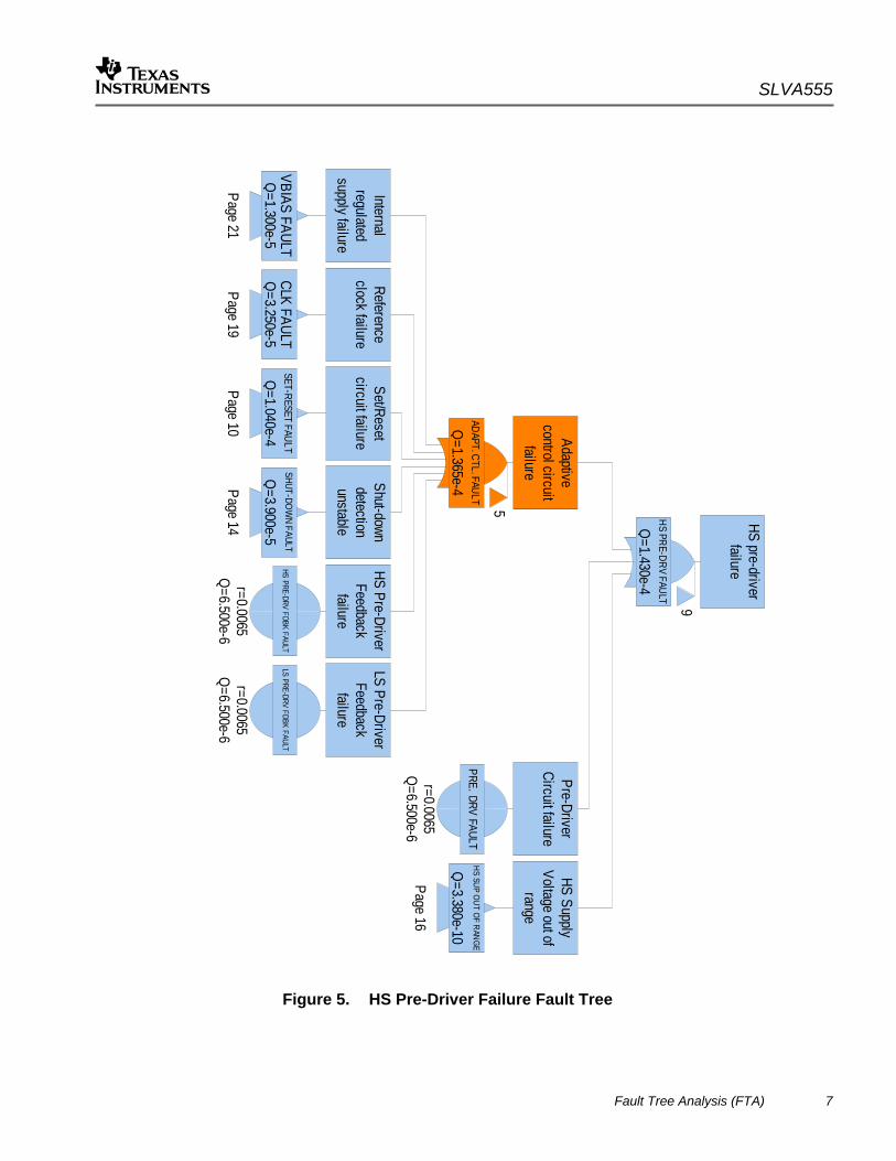
HS PRE-DRV FAULT
Q=1.430e-4
HS pre-driverfailure
9
ADAPT. CTL. FAULT
Q=1.365e-4
Adaptivecontrol circuit
failure
5HS SUP OUT OF RANGE
Q=3.380e-10
HS SupplyVoltage out of
range
Page 16
PRE. DRV FAULT
Pre-DriverCircuit failure
r=0.0065Q
=6.500e-6
VBIAS FAULTQ
=1.300e-5
Internalregulated
supply failure
Page 21
CLK FAULTQ
=3.250e-5
Referenceclock failure
Page 19
SET-RESET FAULT
Q=1.040e-4
Set/Resetcircuit failure
Page 10
SHUT-DOW
N FAULT
Q=3.900e-5
Shut-downdetectionunstable
Page 14
HS PRE-DRV FDBK FAULT
HS Pre-DriverFeedback
failure
r=0.0065Q
=6.500e-6
LS PRE-DRV FDBK FAULT
LS Pre-DriverFeedback
failure
r=0.0065Q
=6.500e-6
Figure 5. HS Pre-Driver Failure Fault Tree
SLVA555
8 Fault Tree Analysis (FTA)
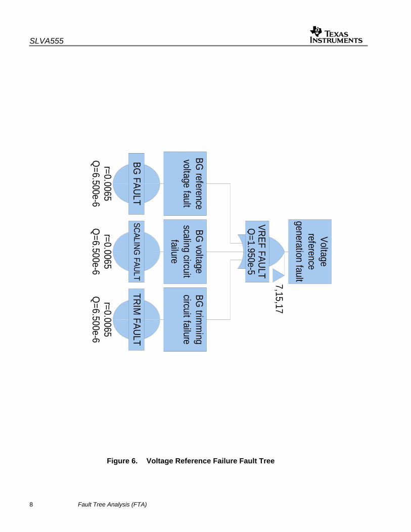
VREF FAULTQ
=1.950e-5
Voltagereference
generation fault7,15,17
BG FAULT
BG reference
voltage fault
r=0.0065Q
=6.500e-6
SCALING FAULT
BG voltage
scaling circuitfailure
r=0.0065Q
=6.500e-6
TRIM FAULT
BG trim
ming
circuit failure
r=0.0065Q
=6.500e-6
Figure 6. Voltage Reference Failure Fault Tree
SLVA555
Fault Tree Analysis (FTA) 9
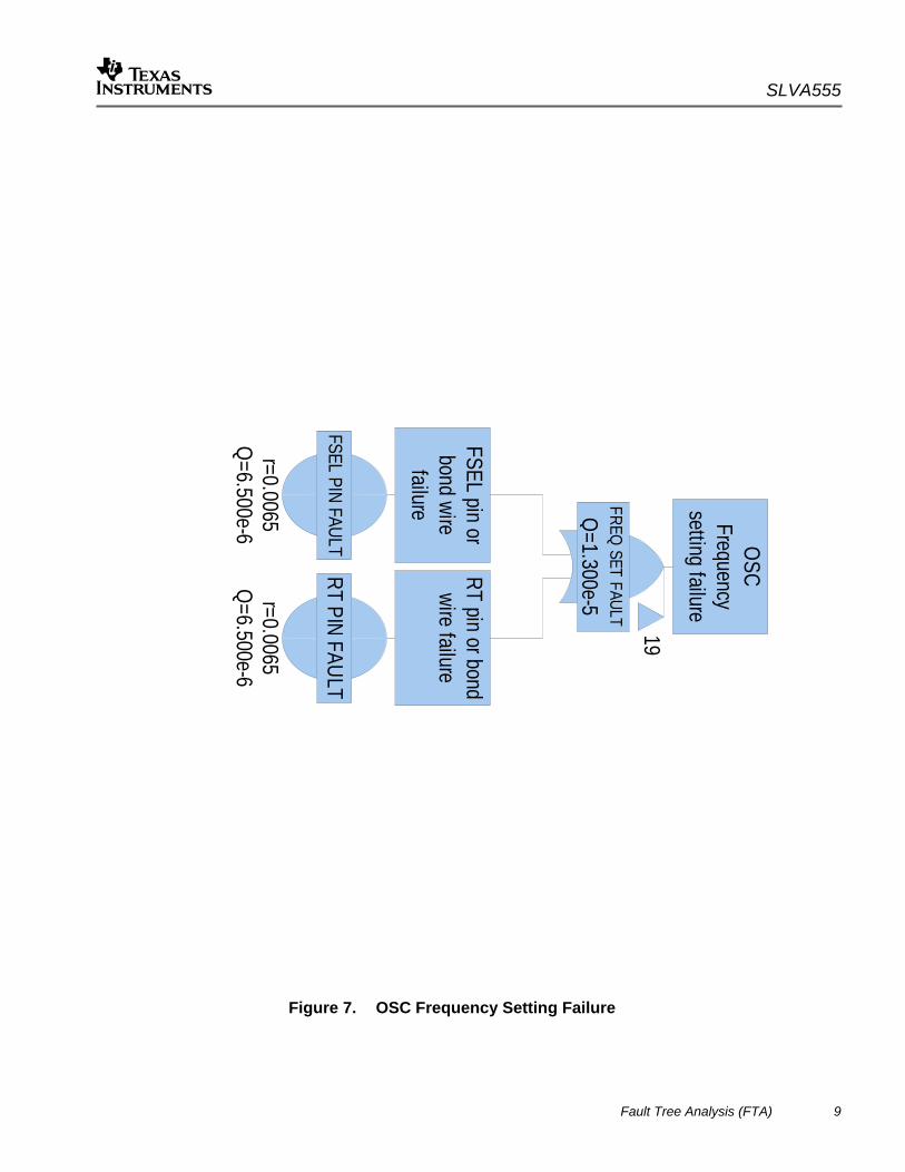
FREQ SET FAULTQ=1.300e-5
OSCFrequency
setting failure
19
FSEL PIN FAULT
FSEL pin orbond wire
failure
r=0.0065Q=6.500e-6
RT PIN FAULT
RT pin or bondwire failure
r=0.0065Q=6.500e-6
Figure 7. OSC Frequency Setting Failure
SLVA555
10 Fault Tree Analysis (FTA)
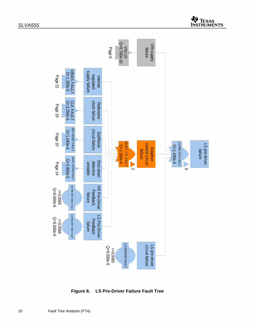
LS PRE-DRV FAULT
Q=1.430e-4
LS pre-driverfailure
9
VBIAS FAULTQ
=1.300e-5
Internalregulated
supply failure
Page 21
CLK FAULTQ
=3.250e-5
Referenceclock failure
Page 19
SET-RESET FAULT
Q=1.040e-4
Set/Resetcircuit failure
Page 10
SHUT-DOW
N FAULT
Q=3.900e-5
Shut-downdetectionunstable
Page 14
HS PRE-DRV FDBK FAULT
HS Pre-DriverFeedback
failure
r=0.0065Q
=6.500e-6
LS PRE-DRV FDBK FAULT
LS Pre-DriverFeedback
failure
r=0.0065Q
=6.500e-6
VIN UVQ
=6.760e-10
VIN supplyfailure
Page 6
ADAPT. CTL. FAULT
Q=1.365e-4
Adaptivecontrol circuit
failure
2
LS DRIVER FAULT
LS pre-drivercircuit failure
r=0.0065Q
=6.500e-6
Figure 8. LS Pre-Driver Failure Fault Tree
SLVA555
Fault Tree Analysis (FTA) 11
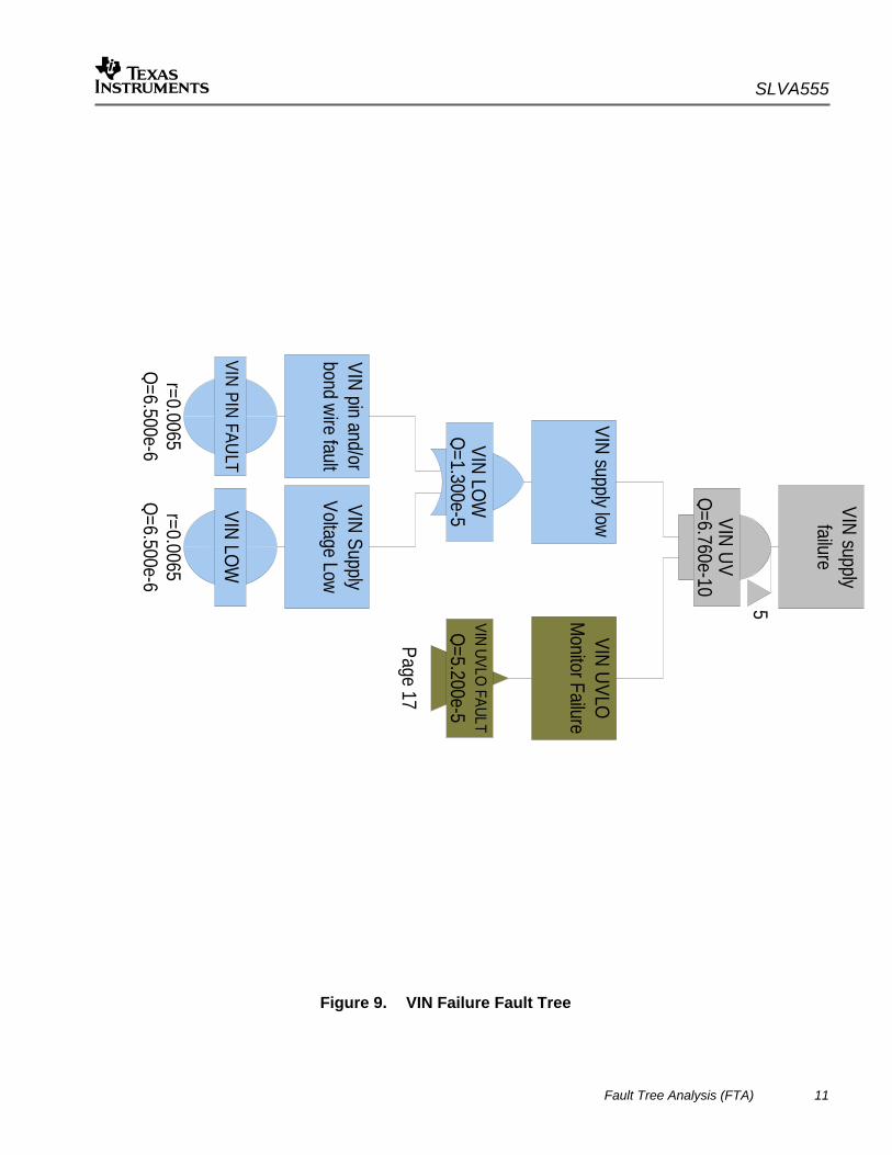
VIN UVQ=6.760e-10
VIN supplyfailure
5
VIN LOWQ=1.300e-5
VIN supply low
VIN UVLO FAULTQ=5.200e-5
VIN UVLOM
onitor Failure
Page 17
VIN PIN FAULT
VIN pin and/orbond wire fault
r=0.0065Q=6.500e-6
VIN LOW
VIN SupplyVoltage Low
r=0.0065Q=6.500e-6
Figure 9. VIN Failure Fault Tree

SLVA555
12 Fault Tree Analysis (FTA)
VSENSE PWRG
D DET. FAULT
Q=4.550e-5
VSENSE PWRG
Ddetection circuit
failure
13
VBIAS FAULTQ
=1.300e-5
Internalregulated
supply failure
Page 21
VREF FAULTQ
=1.950e-5
Voltagereference
generation fault
Page 3
VSENSE COM
P FAULT
VSENSE PWRG
Dcom
paratorfailure
r=0.0065Q
=6.500e-6
VSENSE PIN FAULT
VSENSE pinand/or bond
wire fault
r=0.0065Q
=6.500e-6
Figure 10. VSENSE Power Good Detection failure fault tree
SLVA555
Fault Tree Analysis (FTA) 13
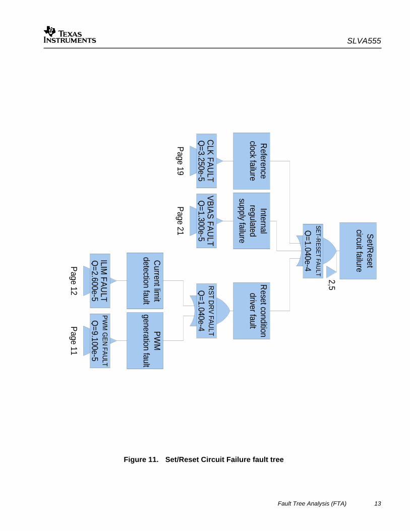
SET-RESET FAU
LT
Q=1.040e-4
Set/Reset
circuit failure
2,5
CLK FAU
LTQ
=3.250e-5
Reference
clock failure
Page 19
VBIAS FAULT
Q=1.300e-5
Internalregulated
supply failure
Page 21
RST DR
V FAULT
Q=1.040e-4
Reset conditiondriver fault
ILIM FAU
LTQ
=2.600e-5
Current lim
itdetection fault
Page 12
PWM
GEN FAULT
Q=9.100e-5
PWM
generation fault
Page 11
Figure 11. Set/Reset Circuit Failure fault tree
SLVA555
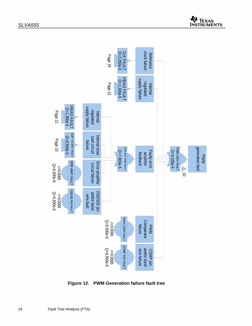
14 Fault Tree Analysis (FTA)
PWM
GEN FAULT
Q=9.100e-5
PWM
generation fault10
CLK FAULTQ
=3.250e-5
Referenceclock failure
Page 19
VBIAS FAULTQ
=1.300e-5
Internalregulated
supply failure
Page 21
ERR AMP FDBK FAULT
Q=7.800e-5
Faulty erroram
plifierfeedback
PWM
COMP FAULT
PWM
Comparator
failure
r=0.0065Q
=6.500e-6
COM
P PIN FAULT
COM
P pinand/or bondwire failure
r=0.0065Q
=6.500e-6
VBIAS FAULTQ
=1.300e-5
Internalregulated
supply failure
Page 21
SOFT START FAULT
Q=6.500e-5
Internal slowstart circuit
failure
Page 15
ERR AMP FAULT
Error amplifier
circuit failure
r=0.0065Q
=6.500e-6
VSENSE PIN FAULT
VSENSE pinand/or bond
wire fault
r=0.0065Q
=6.500e-6
Figure 12. PWM Generation failure fault tree
SLVA555
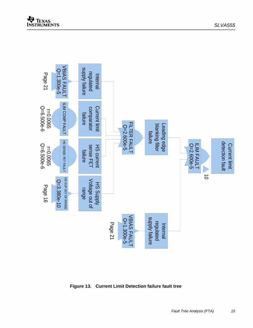
Fault Tree Analysis (FTA) 15
ILIM FAU
LTQ
=2.600e-5
Current lim
itdetection fault
10
FILTER FAULTQ
=2.600e-5
Leading edgeblanking filter
failure
VBIAS FAULT
Q=1.300e-5
Internalregulated
supply failure
Page 21
VBIAS FAULT
Q=1.300e-5
Internalregulated
supply failure
Page 21
HS SUP OUT OF RANGE
Q=3.380e-10
HS Supply
Voltage out ofrange
Page 16
ILIM CO
MP FAULT
Current lim
itcom
paratorfailure
r=0.0065Q
=6.500e-6
HS SENSE FET FAULT
HS current
sense FETfailure
r=0.0065Q
=6.500e-6
Figure 13. Current Limit Detection failure fault tree
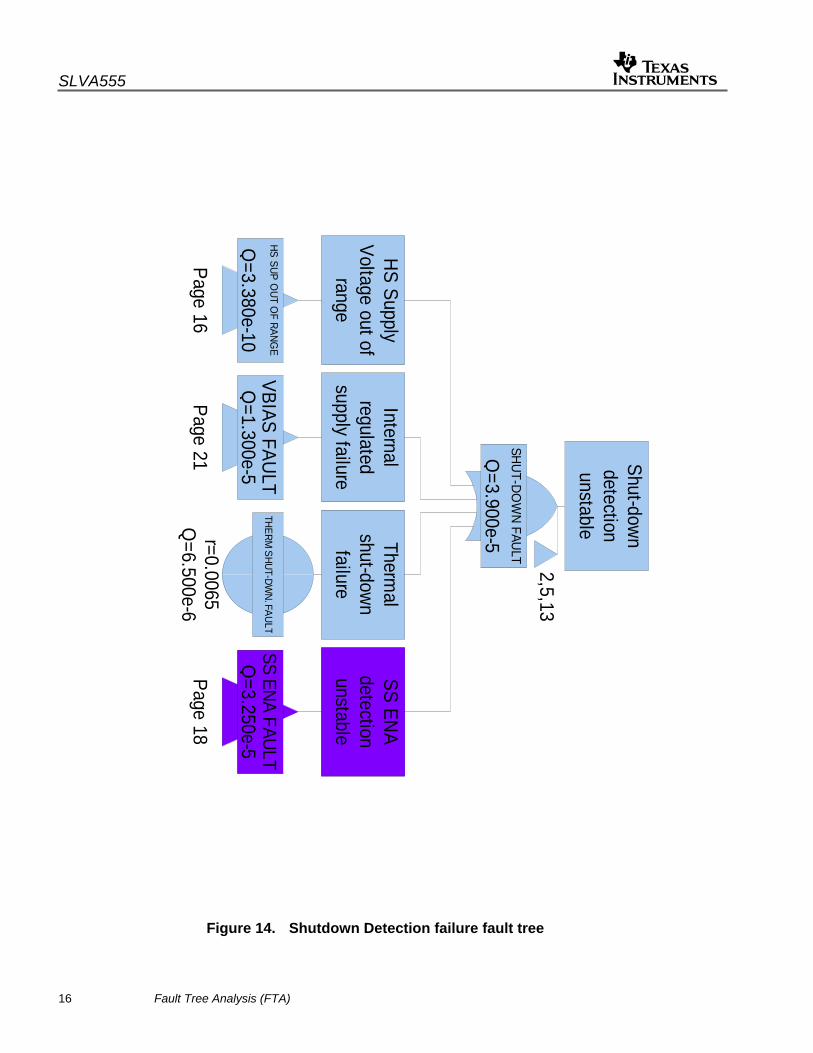
SLVA555
16 Fault Tree Analysis (FTA)
SHUT-DOW
N FAULT
Q=3.900e-5
Shut-downdetectionunstable
2,5,13
HS SUP OUT O
F RANGE
Q=3.380e-10
HS SupplyVoltage out of
range
Page 16
VBIAS FAULTQ
=1.300e-5
Internalregulated
supply failure
Page 21
SS ENA FAULTQ
=3.250e-5
SS ENAdetectionunstable
Page 18
THERM SHUT-DW
N. FAULT
Thermal
shut-downfailure
r=0.0065Q
=6.500e-6
Figure 14. Shutdown Detection failure fault tree
SLVA555
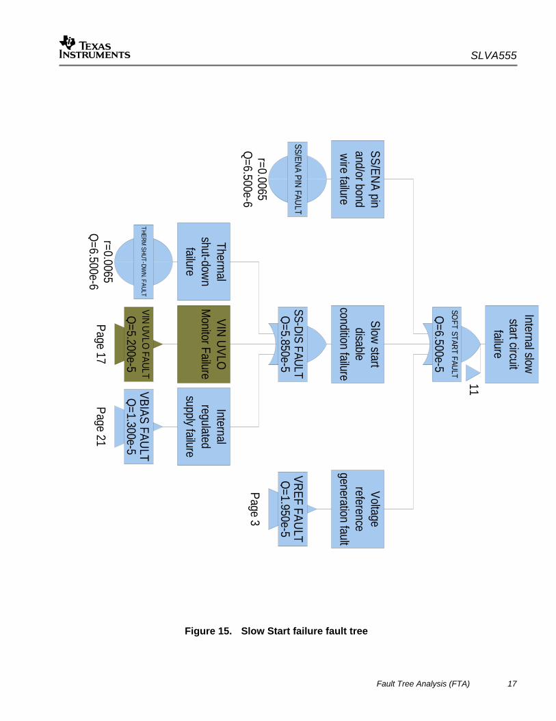
Fault Tree Analysis (FTA) 17
SOFT START FAULT
Q=6.500e-5
Internal slowstart circuit
failure
11
SS-DIS FAULTQ=5.850e-5
Slow startdisable
condition failure
VREF FAULTQ=1.950e-5
Voltagereference
generation fault
Page 3
SS/ENA PIN FAULT
SS/ENA pinand/or bondwire failure
r=0.0065Q=6.500e-6
VIN UVLO FAULTQ=5.200e-5
VIN UVLOM
onitor Failure
Page 17
VBIAS FAULTQ=1.300e-5
Internalregulated
supply failure
Page 21
THERM SHUT-DW
N. FAULT
Thermal
shut-downfailure
r=0.0065Q=6.500e-6
Figure 15. Slow Start failure fault tree
SLVA555
18 Fault Tree Analysis (FTA)
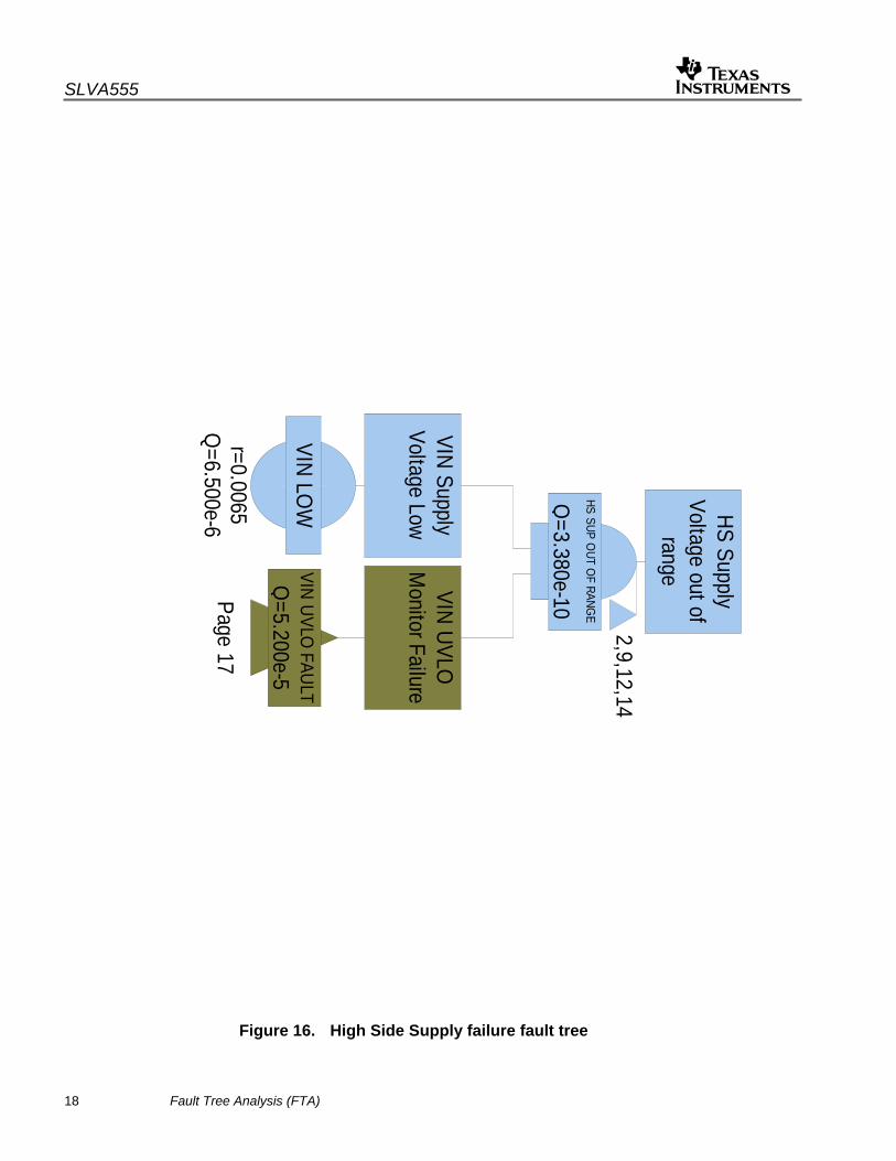
HS SUP OUT O
F RANGE
Q=3.380e-10
HS SupplyVoltage out of
range
2,9,12,14
VIN UVLO FAULTQ
=5.200e-5
VIN UVLOM
onitor Failure
Page 17
VIN LOW
VIN SupplyVoltage Low
r=0.0065Q
=6.500e-6
Figure 16. High Side Supply failure fault tree
SLVA555
Fault Tree Analysis (FTA) 19
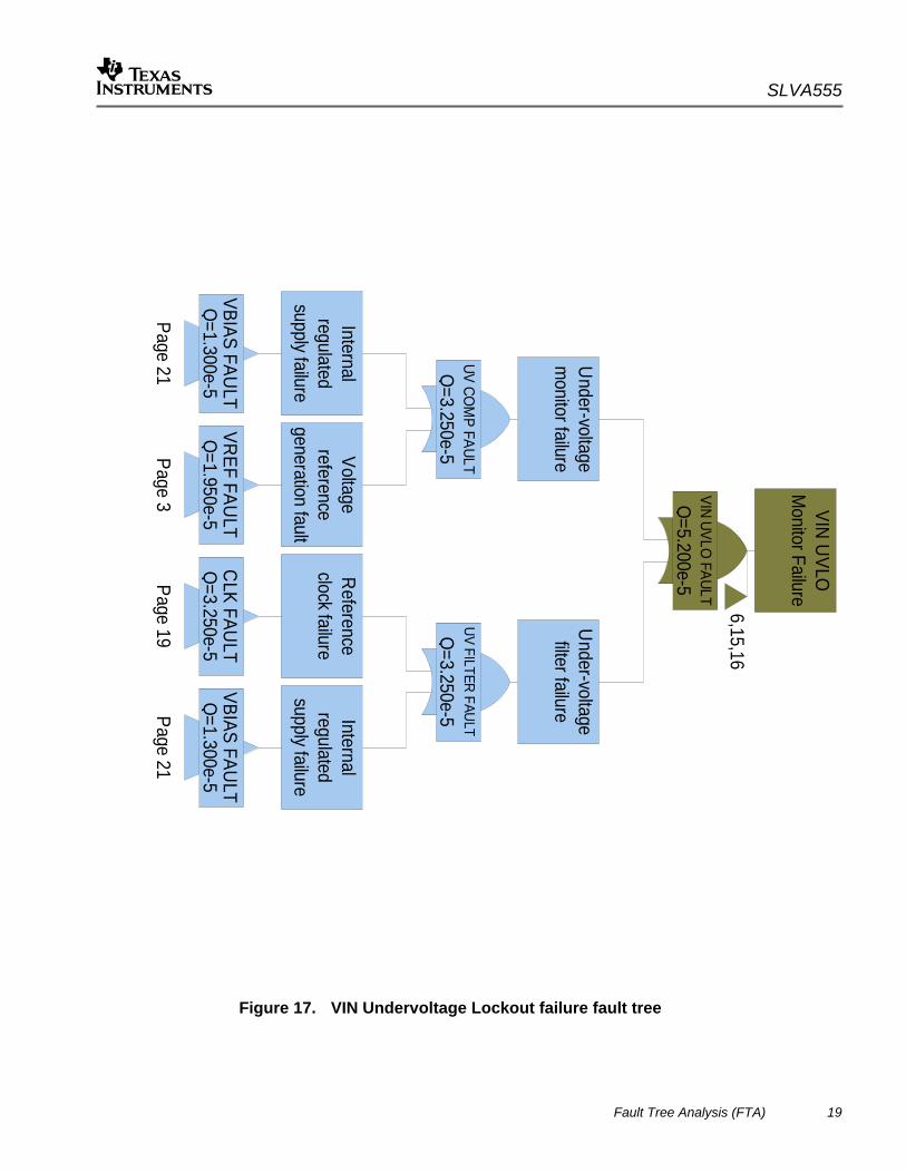
VIN UVLO FAULT
Q=5.200e-5
VIN U
VLOM
onitor Failure
6,15,16
UV COM
P FAULTQ
=3.250e-5
Under-voltage
monitor failure
UV FILTER FAULTQ
=3.250e-5
Under-voltagefilter failure
VBIAS FAULTQ
=1.300e-5
Internalregulated
supply failure
Page 21
VREF FAULT
Q=1.950e-5
Voltagereference
generation fault
Page 3
CLK FAU
LTQ
=3.250e-5
Reference
clock failure
Page 19
VBIAS FAULTQ
=1.300e-5
Internalregulated
supply failure
Page 21
Figure 17. VIN Undervoltage Lockout failure fault tree
SLVA555
20 Fault Tree Analysis (FTA)
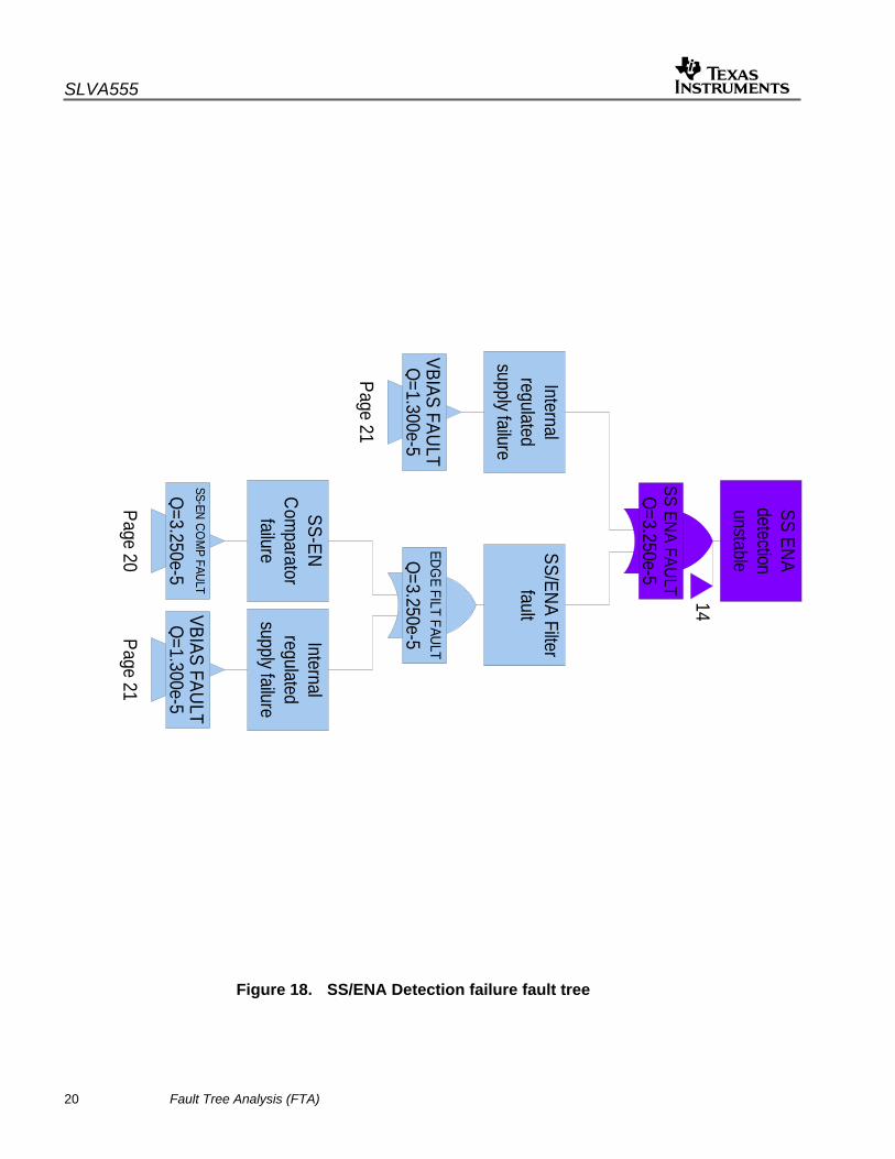
SS ENA FAULTQ=3.250e-5
SS ENAdetectionunstable
14
VBIAS FAULTQ=1.300e-5
Internalregulated
supply failure
Page 21
EDGE FILT FAULT
Q=3.250e-5
SS/ENA Filterfault
SS-EN COM
P FAULT
Q=3.250e-5
SS-ENCom
paratorfailure
Page 20
VBIAS FAULTQ=1.300e-5
Internalregulated
supply failure
Page 21
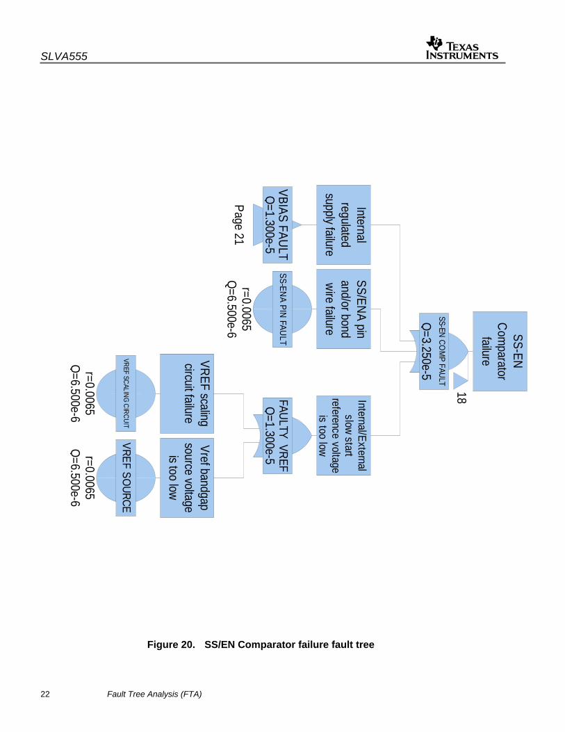
Figure 18. SS/ENA Detection failure fault tree
SLVA555
Fault Tree Analysis (FTA) 21
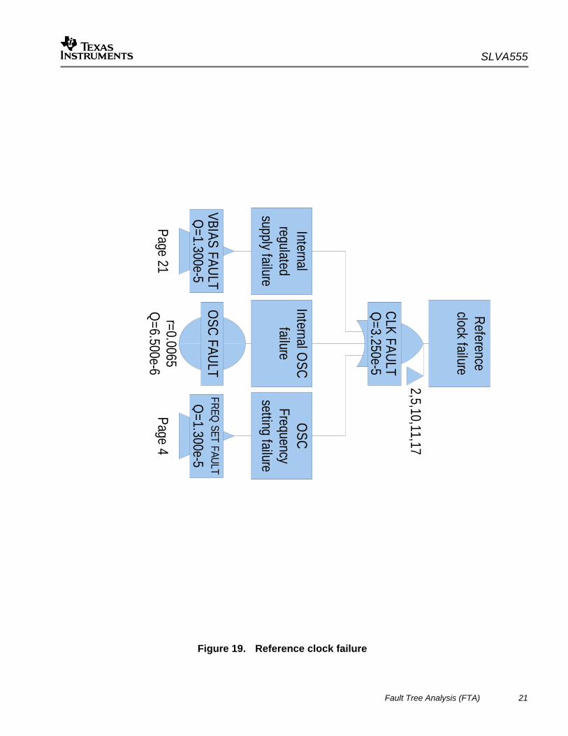
CLK FAULTQ=3.250e-5
Referenceclock failure
2,5,10,11,17
VBIAS FAULTQ=1.300e-5
Internalregulated
supply failure
Page 21
FREQ SET FAULTQ=1.300e-5
OSCFrequency
setting failure
Page 4
OSC FAULT
Internal OSCfailure
r=0.0065Q=6.500e-6
Figure 19. Reference clock failure
SLVA555
22 Fault Tree Analysis (FTA)
SS-EN COM
P FAULT
Q=3.250e-5
SS-ENCom
paratorfailure
18
VREF SCALING CIRCUIT
VREF scalingcircuit failure
r=0.0065Q=6.500e-6
VREF SOURCE
Vref bandgapsource voltage
is too low
r=0.0065Q=6.500e-6
VBIAS FAULTQ=1.300e-5
Internalregulated
supply failure
Page 21
FAULTY VREFQ=1.300e-5
Internal/Externalslow start
reference voltageis too low
SS-ENA PIN FAULT
SS/ENA pinand/or bondwire failure
r=0.0065Q=6.500e-6
Figure 20. SS/EN Comparator failure fault tree
SLVA555
Fault Tree Analysis (FTA) 23
VBIAS FAULTQ=1.300e-5
Internalregulated
supply failure
2,5,7,10,11,12,13,14,15,17,...
REG FAULT
Internal VBIASREG Failure
r=0.0065Q=6.500e-6
VBIAS PIN FAULT
VBIAS pin orbond wire fault
r=0.0065Q=6.500e-6
Figure 21. Internal Regulator failure fault tree
SLVA555
24 Fault Tree Analysis (FTA)
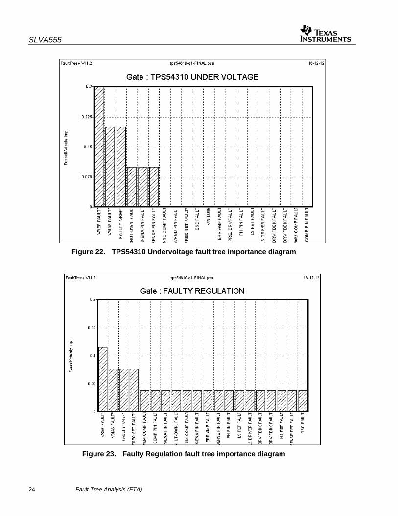
Figure 22. TPS54310 Undervoltage fault tree importance diagram
Figure 23. Faulty Regulation fault tree importance diagram
SLVA555
Fault Tree Analysis (FTA) 25
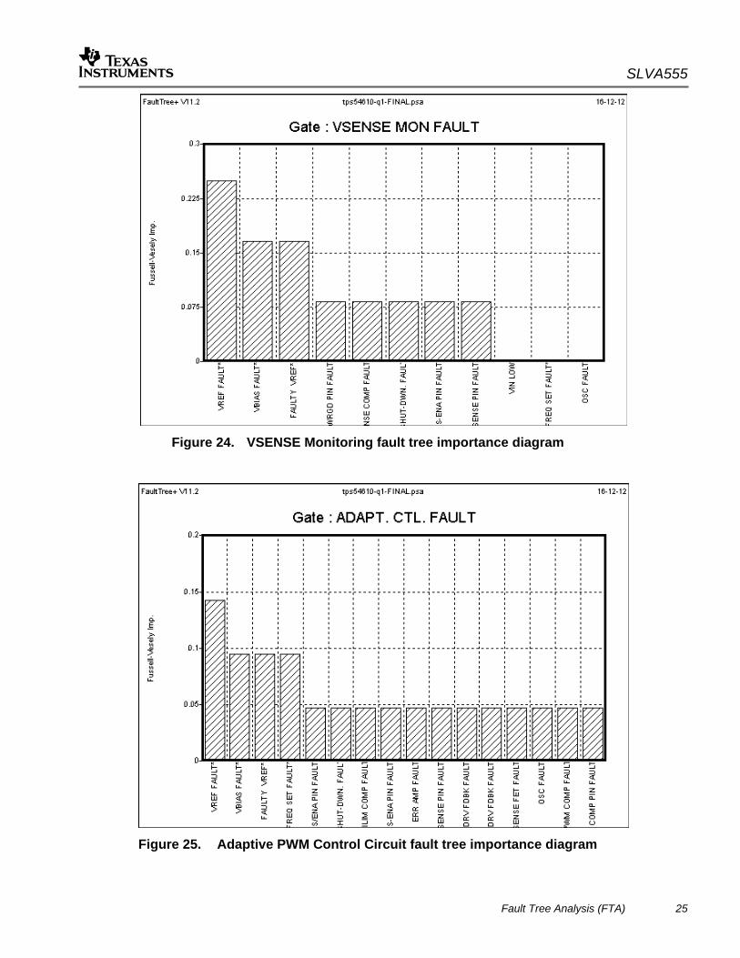
Figure 24. VSENSE Monitoring fault tree importance diagram
Figure 25. Adaptive PWM Control Circuit fault tree importance diagram
SLVA555
26 Fault Tree Analysis (FTA)
3 Hazards
a. Faulty Switch Regulator leading to undervoltage condition
4 Analysis
4.1 Description
Cut Set: A group of events which will cause system failure when occurring together. 1st Order Cut Set: Single event failure causing hazard. 2nd Order Cut Set: Two failing events causing hazard. 3rd Order Cut Set: Three failing events causing hazard. 4th Order Cut Set: Four failing events causing hazard.
Base Event: Description of base events in associated fault tree diagram. Base events and their description referenced to TI’s design database.
4.2 Faulty Switch Regulator Cut Sets
Hazard: Faulty Switch regulator leading to under voltage condition.
For this hazard a total 36 individual cut sets have been analyzed.
5 Conclusion
ASIC level hazard FTA completed. Switch regulator proactive system level monitoring and protection considerations were included.
IMPORTANT NOTICE
Texas Instruments Incorporated and its subsidiaries (TI) reserve the right to make corrections, enhancements, improvements and otherchanges to its semiconductor products and services per JESD46, latest issue, and to discontinue any product or service per JESD48, latestissue. Buyers should obtain the latest relevant information before placing orders and should verify that such information is current andcomplete. All semiconductor products (also referred to herein as “components”) are sold subject to TI’s terms and conditions of salesupplied at the time of order acknowledgment.
TI warrants performance of its components to the specifications applicable at the time of sale, in accordance with the warranty in TI’s termsand conditions of sale of semiconductor products. Testing and other quality control techniques are used to the extent TI deems necessaryto support this warranty. Except where mandated by applicable law, testing of all parameters of each component is not necessarilyperformed.
TI assumes no liability for applications assistance or the design of Buyers’ products. Buyers are responsible for their products andapplications using TI components. To minimize the risks associated with Buyers’ products and applications, Buyers should provideadequate design and operating safeguards.
TI does not warrant or represent that any license, either express or implied, is granted under any patent right, copyright, mask work right, orother intellectual property right relating to any combination, machine, or process in which TI components or services are used. Informationpublished by TI regarding third-party products or services does not constitute a license to use such products or services or a warranty orendorsement thereof. Use of such information may require a license from a third party under the patents or other intellectual property of thethird party, or a license from TI under the patents or other intellectual property of TI.
Reproduction of significant portions of TI information in TI data books or data sheets is permissible only if reproduction is without alterationand is accompanied by all associated warranties, conditions, limitations, and notices. TI is not responsible or liable for such altereddocumentation. Information of third parties may be subject to additional restrictions.
Resale of TI components or services with statements different from or beyond the parameters stated by TI for that component or servicevoids all express and any implied warranties for the associated TI component or service and is an unfair and deceptive business practice.TI is not responsible or liable for any such statements.
Buyer acknowledges and agrees that it is solely responsible for compliance with all legal, regulatory and safety-related requirementsconcerning its products, and any use of TI components in its applications, notwithstanding any applications-related information or supportthat may be provided by TI. Buyer represents and agrees that it has all the necessary expertise to create and implement safeguards whichanticipate dangerous consequences of failures, monitor failures and their consequences, lessen the likelihood of failures that might causeharm and take appropriate remedial actions. Buyer will fully indemnify TI and its representatives against any damages arising out of the useof any TI components in safety-critical applications.
In some cases, TI components may be promoted specifically to facilitate safety-related applications. With such components, TI’s goal is tohelp enable customers to design and create their own end-product solutions that meet applicable functional safety standards andrequirements. Nonetheless, such components are subject to these terms.
No TI components are authorized for use in FDA Class III (or similar life-critical medical equipment) unless authorized officers of the partieshave executed a special agreement specifically governing such use.
Only those TI components which TI has specifically designated as military grade or “enhanced plastic” are designed and intended for use inmilitary/aerospace applications or environments. Buyer acknowledges and agrees that any military or aerospace use of TI componentswhich have not been so designated is solely at the Buyer's risk, and that Buyer is solely responsible for compliance with all legal andregulatory requirements in connection with such use.
TI has specifically designated certain components as meeting ISO/TS16949 requirements, mainly for automotive use. In any case of use ofnon-designated products, TI will not be responsible for any failure to meet ISO/TS16949.
Products Applications
Audio www.ti.com/audio Automotive and Transportation www.ti.com/automotive
Amplifiers amplifier.ti.com Communications and Telecom www.ti.com/communications
Data Converters dataconverter.ti.com Computers and Peripherals www.ti.com/computers
DLP® Products www.dlp.com Consumer Electronics www.ti.com/consumer-apps
DSP dsp.ti.com Energy and Lighting www.ti.com/energy
Clocks and Timers www.ti.com/clocks Industrial www.ti.com/industrial
Interface interface.ti.com Medical www.ti.com/medical
Logic logic.ti.com Security www.ti.com/security
Power Mgmt power.ti.com Space, Avionics and Defense www.ti.com/space-avionics-defense
Microcontrollers microcontroller.ti.com Video and Imaging www.ti.com/video
RFID www.ti-rfid.com
OMAP Applications Processors www.ti.com/omap TI E2E Community e2e.ti.com
Wireless Connectivity www.ti.com/wirelessconnectivity
Mailing Address: Texas Instruments, Post Office Box 655303, Dallas, Texas 75265Copyright © 2012, Texas Instruments Incorporated