experiment 12 priority encoders - welcome to matcecampus.matc.edu/lokkenr/elctec-131/labs/experiment...
TRANSCRIPT
ELCTEC-131 Advanced Digital Electronics MATC Richard Lokken Adapted for the DE1 board
Experiment 12 Priority Encoders
Objectives
Upon completion of this laboratory exercise, you should be able to:
Enter a VHDL design for a BCD priority encoder.
Write simulation criteria for the BCD priority encoder and create a simulation in Quartus II.
Create a test circuit for the BCD priority encoder in the Quartus II Block Editor.
Test the priority encoder on a CPLD test board.
Lab Reference and Equipment Required
Dueck, Robert K., Digital Design with CPLD Applications and VHDL, 2/e
o Chapter 6: Combinational Logic Functions
6.2 Encoders CPLD Trainer:
o Altera DE1 with Altera EP2C20F484C7 CPLD Quartus II Web Edition software
Experimental Notes
In this lab, we will examine the behavior of a priority encoder. This circuit can be easily implemented in VHDL and with more difficulty in a Quartus II Block Diagram File. A priority encoder becomes much more complex with each additional input bit, so it is often easiest to use various VHDL constructs that describe the behavior of each circuit, rather than its specific Boolean equations.
A priority encoder is a circuit that generates a binary or BCD code that corresponds to the active input with the highest priority, which generally means the active
ELCTEC-131 Advanced Digital Electronics MATC Richard Lokken Adapted for the DE1 board
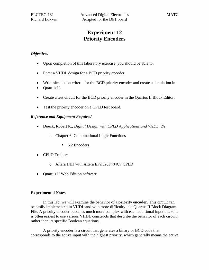
input with the highest decimal subscript. Figure 12.1 shows an example of the operation of a BCD priority encoder.
In Figure 12.1a, only input D2 is active, so the output code generated is 0010, the
binary equivalent of 2. In Figure 12.1b, input D2 remains active, but now D7 is also active. Since D7 has the higher priority, the output code is now 0111, the binary equivalent of 7. In Figure 12.1c, input D9 is HIGH, in addition to the other two inputs. Since D9 has the highest priority, the output is 1001. There is no input for D0 since the output 0000 is the default value when no inputs are active.
Procedure Design Entry and Simulation
1. Refer to the section on VHDL priority encoders in Digital Design with CPLD Applications and VHDL, 2/e (pp. 294–296). Write a VHDL file for a BCD priority encoder and save it as drive:\qdesigns\labs\lab12\hipri10\hipri10.vhd. Do not use concurrent signal assignment statements (i.e., do not directly code the Boolean equations for the encoder).
2. Save and compile the project.
3. Write a set of simulation criteria that will test the correctness of the priority
encoder design. Simulation Criteria
ELCTEC-131 Advanced Digital Electronics MATC Richard Lokken Adapted for the DE1 board
4. Use the simulation criteria you wrote in step 3 to create a Quartus II simulation of the BCD priority encoder.
Test Circuit for Priority Encoder
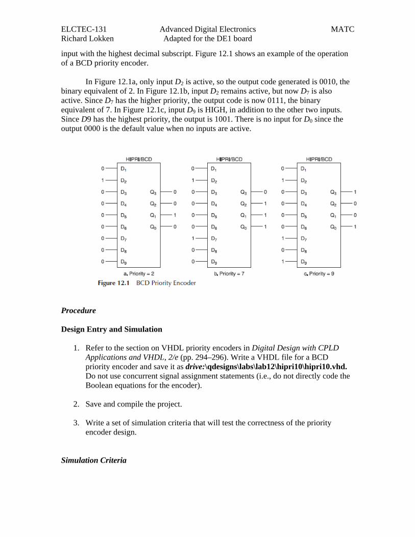
Figure 12.2 shows a test circuit with active-LOW LED outputs for the BCD priority encoder that can be used with the Altera UP-2 or DeVry eSOC boards. Figure 12.3 shows a test circuit with active-HIGH LED outputs for the RSR PLDT-2 board. The test circuit displays the output of the priority encoder both as a binary value and as a decimal digit on the board’s seven-segment numerical display. Unused LEDs are disabled by tying them either to VCC or ground, as appropriate for the selected board. The symbols for the priority encoder and the seven-segment decoder are created from VHDL files for those components.
Figure 12.2 Priority Encoder Test Circuit
1. Create a new folder for the test circuit and name it: drive:\qdesigns\labs\lab12\BCD_priority
2. Copy the VHDL file for the priority encoder to the new folder. Also copy the
VHDL file for a hexadecimal-to-seven-segment decoder to the new folder from the folder used for Lab 11 (Binary and Seven-Segment Decoders in VHDL). The decoder should be common anode.
ELCTEC-131 Advanced Digital Electronics MATC Richard Lokken Adapted for the DE1 board
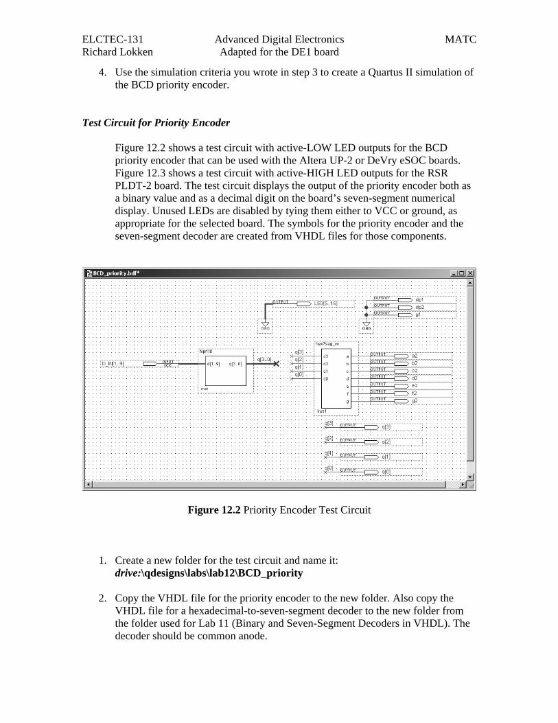
3. Make a project for the test circuit by selecting New Project Wizard from the File menu, as shown in Figure 12.3
Figure 12.3 New Project Wizard (File Menu)
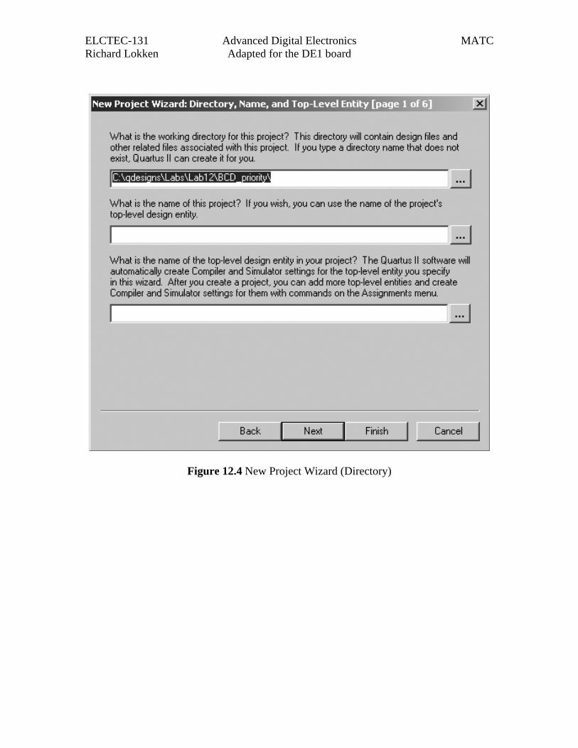
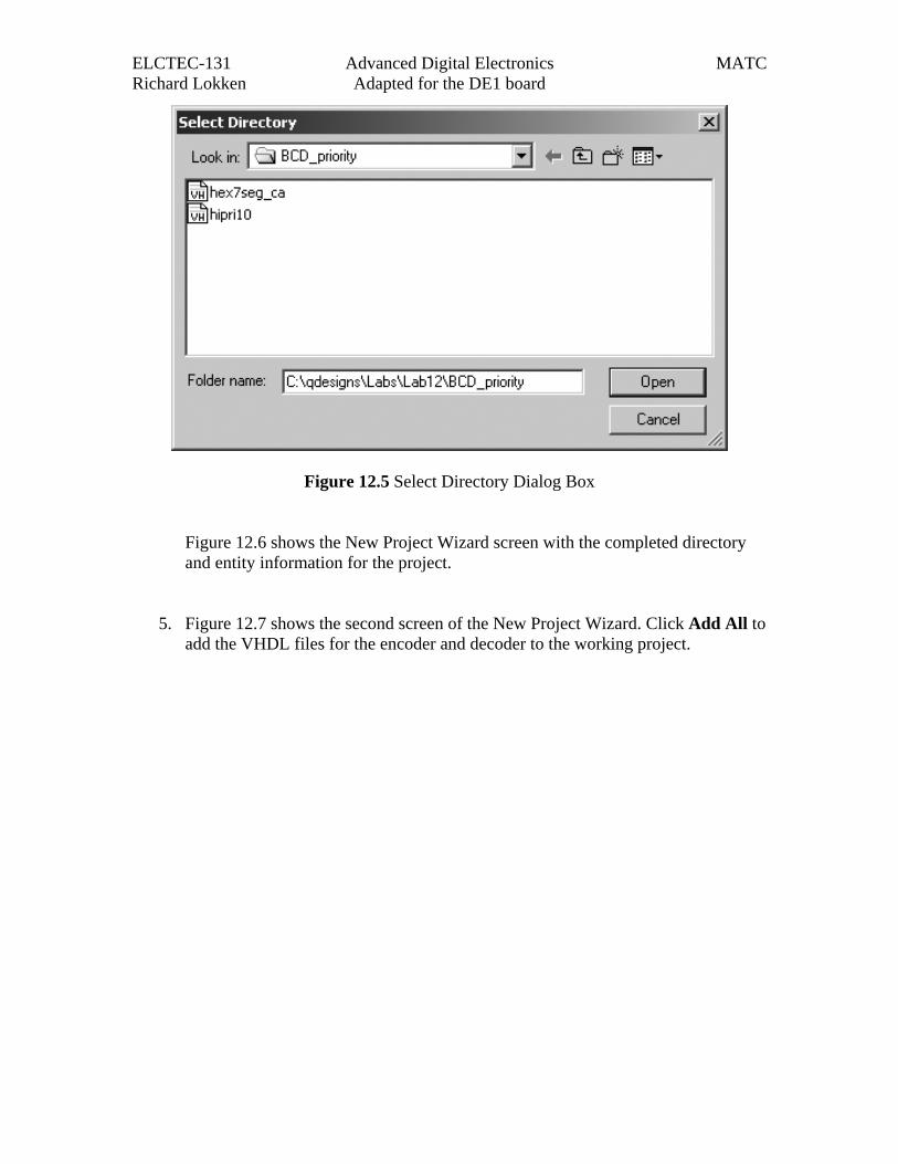
4. In the first screen of the New Project Wizard, shown in Figure 12.4, select the (. . .) button to browse to the new folder, as shown in Figures 12.4 and 12.5. Click Open in the dialog box shown in Figure 12.5 to select the working directory.
ELCTEC-131 Advanced Digital Electronics MATC Richard Lokken Adapted for the DE1 board
Figure 12.4 New Project Wizard (Directory)
ELCTEC-131 Advanced Digital Electronics MATC Richard Lokken Adapted for the DE1 board
Figure 12.5 Select Directory Dialog Box
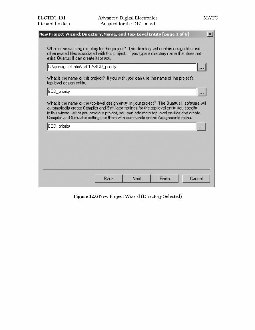
Figure 12.6 shows the New Project Wizard screen with the completed directory and entity information for the project.
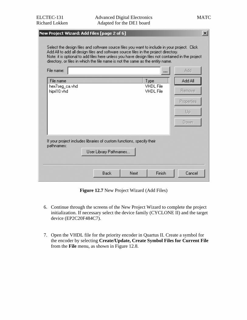
5. Figure 12.7 shows the second screen of the New Project Wizard. Click Add All to add the VHDL files for the encoder and decoder to the working project.
ELCTEC-131 Advanced Digital Electronics MATC Richard Lokken Adapted for the DE1 board
Figure 12.6 New Project Wizard (Directory Selected)
ELCTEC-131 Advanced Digital Electronics MATC Richard Lokken Adapted for the DE1 board
Figure 12.7 New Project Wizard (Add Files)
6. Continue through the screens of the New Project Wizard to complete the project initialization. If necessary select the device family (CYCLONE II) and the target device (EP2C20F484C7).
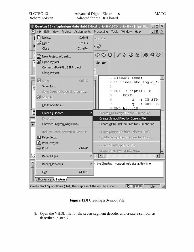
7. Open the VHDL file for the priority encoder in Quartus II. Create a symbol for the encoder by selecting Create/Update, Create Symbol Files for Current File from the File menu, as shown in Figure 12.8.
ELCTEC-131 Advanced Digital Electronics MATC Richard Lokken Adapted for the DE1 board
Figure 12.8 Creating a Symbol File
8. Open the VHDL file for the seven-segment decoder and create a symbol, as described in step 7.
ELCTEC-131 Advanced Digital Electronics MATC Richard Lokken Adapted for the DE1 board
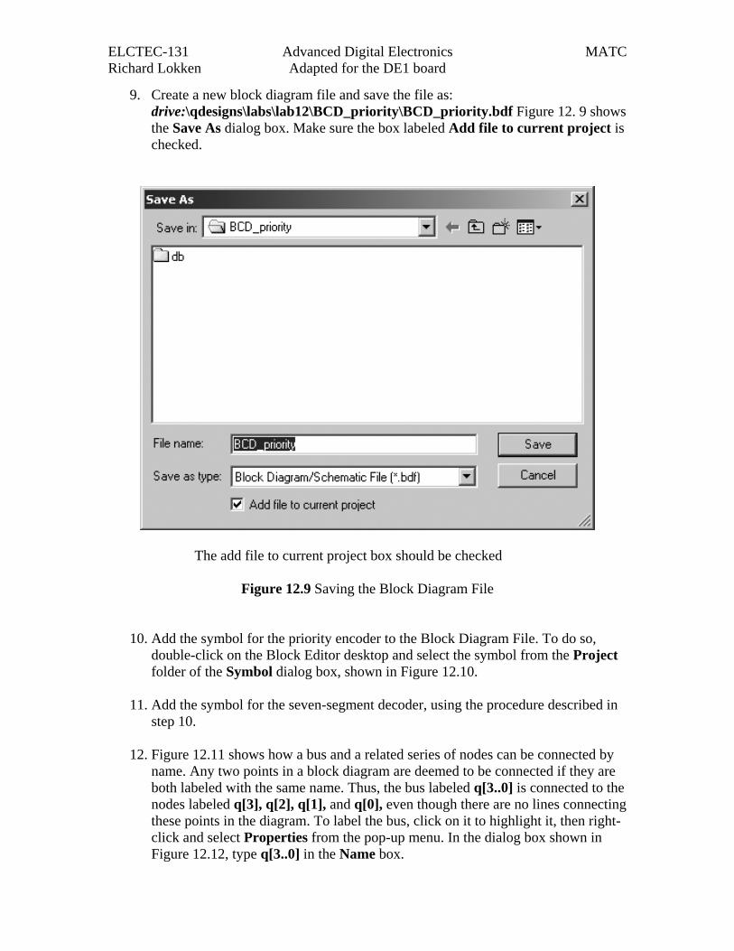
9. Create a new block diagram file and save the file as: drive:\qdesigns\labs\lab12\BCD_priority\BCD_priority.bdf Figure 12. 9 shows the Save As dialog box. Make sure the box labeled Add file to current project is checked.
The add file to current project box should be checked
Figure 12.9 Saving the Block Diagram File
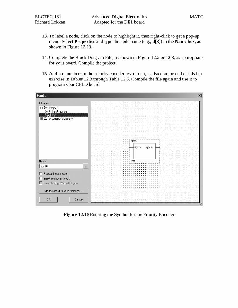
10. Add the symbol for the priority encoder to the Block Diagram File. To do so, double-click on the Block Editor desktop and select the symbol from the Project folder of the Symbol dialog box, shown in Figure 12.10.
11. Add the symbol for the seven-segment decoder, using the procedure described in
step 10.
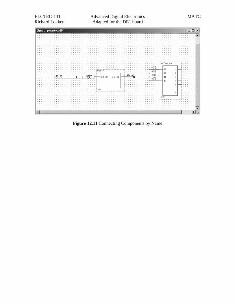
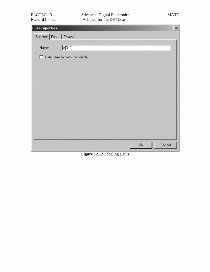
12. Figure 12.11 shows how a bus and a related series of nodes can be connected by name. Any two points in a block diagram are deemed to be connected if they are both labeled with the same name. Thus, the bus labeled q[3..0] is connected to the nodes labeled q[3], q[2], q[1], and q[0], even though there are no lines connecting these points in the diagram. To label the bus, click on it to highlight it, then right-click and select Properties from the pop-up menu. In the dialog box shown in Figure 12.12, type q[3..0] in the Name box.
ELCTEC-131 Advanced Digital Electronics MATC Richard Lokken Adapted for the DE1 board
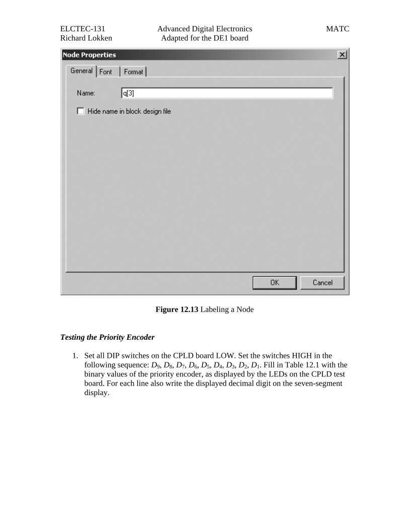
13. To label a node, click on the node to highlight it, then right-click to get a pop-up
menu. Select Properties and type the node name (e.g., d[3]) in the Name box, as shown in Figure 12.13.
14. Complete the Block Diagram File, as shown in Figure 12.2 or 12.3, as appropriate
for your board. Compile the project. 15. Add pin numbers to the priority encoder test circuit, as listed at the end of this lab
exercise in Tables 12.3 through Table 12.5. Compile the file again and use it to program your CPLD board.
Figure 12.10 Entering the Symbol for the Priority Encoder
ELCTEC-131 Advanced Digital Electronics MATC Richard Lokken Adapted for the DE1 board
Figure 12.11 Connecting Components by Name
ELCTEC-131 Advanced Digital Electronics MATC Richard Lokken Adapted for the DE1 board
Figure 12.12 Labeling a Bus
ELCTEC-131 Advanced Digital Electronics MATC Richard Lokken Adapted for the DE1 board
Figure 12.13 Labeling a Node Testing the Priority Encoder
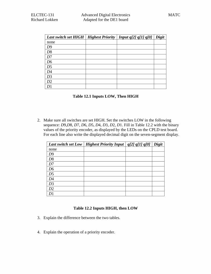
1. Set all DIP switches on the CPLD board LOW. Set the switches HIGH in the following sequence: D9, D8, D7, D6, D5, D4, D3, D2, D1. Fill in Table 12.1 with the binary values of the priority encoder, as displayed by the LEDs on the CPLD test board. For each line also write the displayed decimal digit on the seven-segment display.
ELCTEC-131 Advanced Digital Electronics MATC Richard Lokken Adapted for the DE1 board
Last switch set HIGH Highest Priority Input q[2] q[1] q[0] Digit none D9 D8 D7 D6 D5 D4 D3 D2 D1
Table 12.1 Inputs LOW, Then HIGH
2. Make sure all switches are set HIGH. Set the switches LOW in the following sequence: D9,D8, D7, D6, D5, D4, D3, D2, D1. Fill in Table 12.2 with the binary values of the priority encoder, as displayed by the LEDs on the CPLD test board. For each line also write the displayed decimal digit on the seven-segment display.
Last switch set Low Highest Priority Input q[2] q[1] q[0] Digit none D9 D8 D7 D6 D5 D4 D3 D2 D1
Table 12.2 Inputs HIGH, then LOW
3. Explain the difference between the two tables.
4. Explain the operation of a priority encoder.