euv free-electron laser requirements and considerations ...pf · euv free-electron laser...
TRANSCRIPT
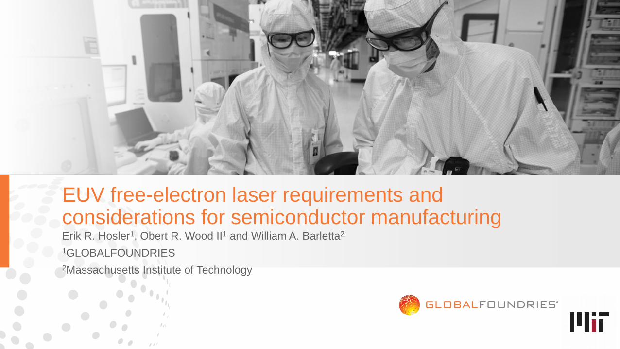
EUV free-electron laser requirements and considerations for semiconductor manufacturing Erik R. Hosler1, Obert R. Wood II1 and William A. Barletta2
1GLOBALFOUNDRIES
2Massachusetts Institute of Technology
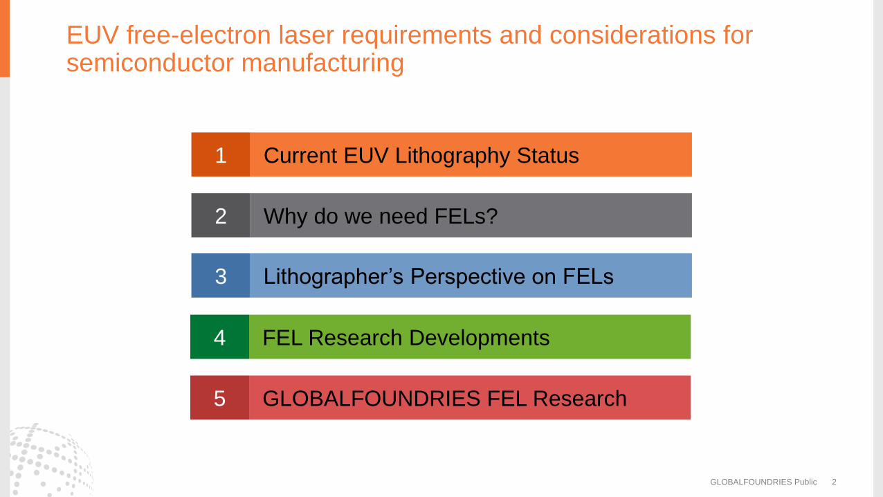
EUV free-electron laser requirements and considerations for semiconductor manufacturing
GLOBALFOUNDRIES Public 2
Current EUV Lithography Status
Why do we need FELs?
Lithographer’s Perspective on FELs
1
2
3
FEL Research Developments 4
GLOBALFOUNDRIES FEL Research 5
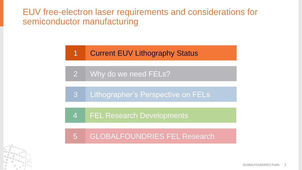
EUV free-electron laser requirements and considerations for semiconductor manufacturing
GLOBALFOUNDRIES Public 3
Current EUV Lithography Status
Why do we need FELs?
Lithographer’s Perspective on FELs
1
2
3
FEL Research Developments 4
GLOBALFOUNDRIES FEL Research 5
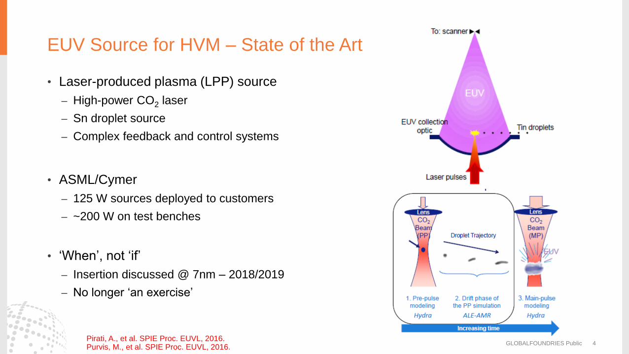
EUV Source for HVM – State of the Art
• Laser-produced plasma (LPP) source
– High-power CO2 laser
– Sn droplet source
– Complex feedback and control systems
• ASML/Cymer
– 125 W sources deployed to customers
– ~200 W on test benches
• ‘When’, not ‘if’
– Insertion discussed @ 7nm – 2018/2019
– No longer ‘an exercise’
GLOBALFOUNDRIES Public 4 Pirati, A., et al. SPIE Proc. EUVL, 2016. Purvis, M., et al. SPIE Proc. EUVL, 2016.
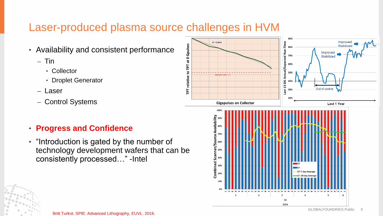
Laser-produced plasma source challenges in HVM
• Availability and consistent performance
– Tin
• Collector
• Droplet Generator
– Laser
– Control Systems
• Progress and Confidence
• “Introduction is gated by the number of technology development wafers that can be consistently processed…” -Intel
GLOBALFOUNDRIES Public 5 Britt Turkot. SPIE: Advanced Lithography, EUVL. 2016.
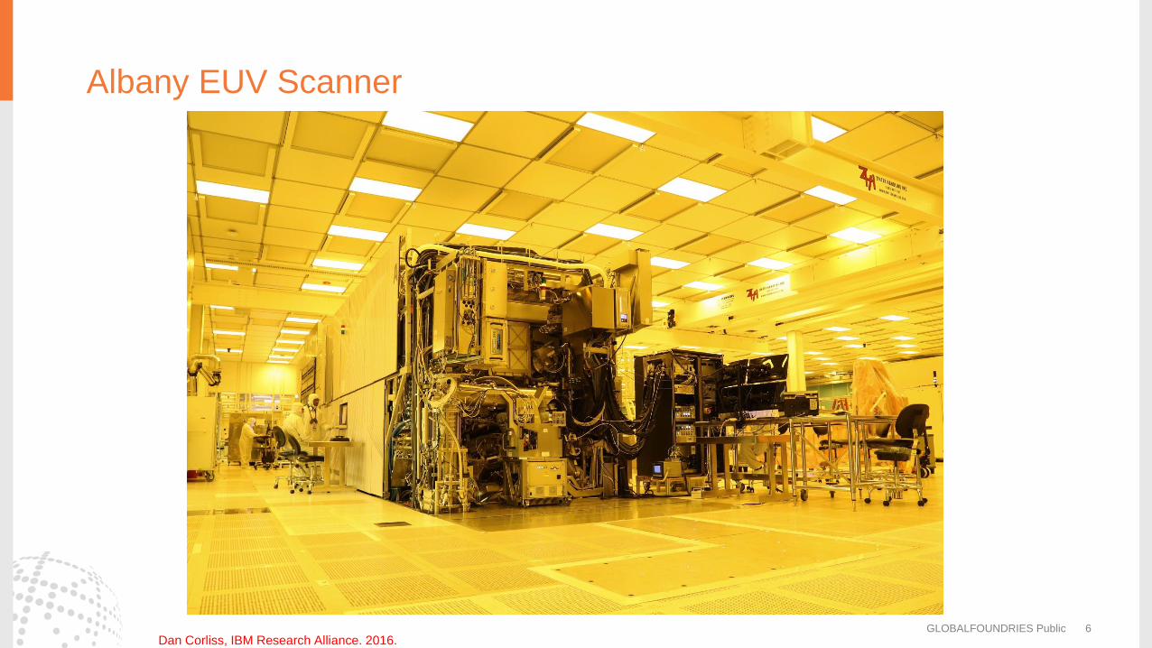
Albany EUV Scanner
GLOBALFOUNDRIES Public 6 Dan Corliss, IBM Research Alliance. 2016.
EUV free-electron laser requirements and considerations for semiconductor manufacturing
GLOBALFOUNDRIES Public 7
Current EUV Lithography Status
Why do we need FELs?
Lithographer’s Perspective on FELs
1
2
3
FEL Research Developments 4
GLOBALFOUNDRIES FEL Research 5
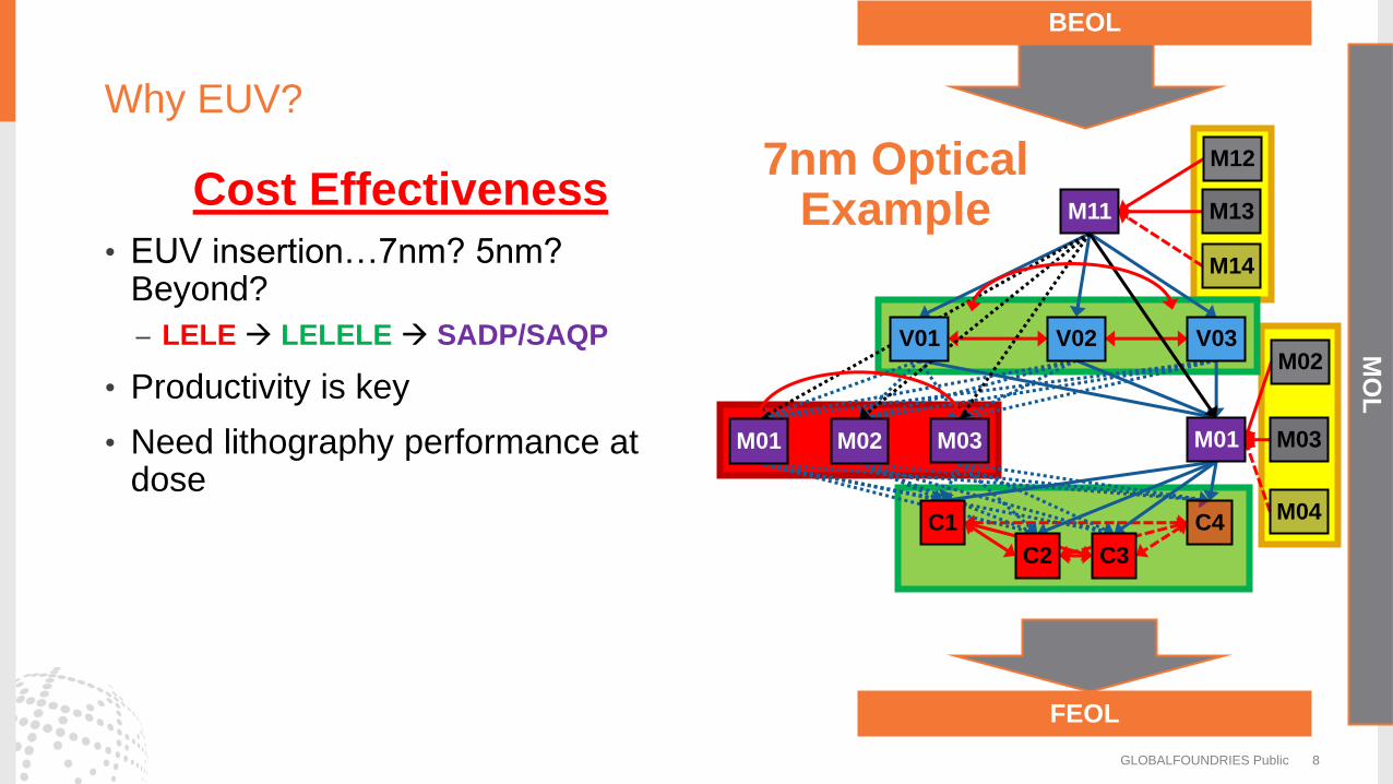
Why EUV?
Cost Effectiveness
• EUV insertion…7nm? 5nm? Beyond?
– LELE LELELE SADP/SAQP
• Productivity is key
• Need lithography performance at dose
GLOBALFOUNDRIES Public 8
7nm Optical Example
FEOL
BEOL
V01 V02 V03
M11
M12
M13
M14
C1
C2 C3
C4
M01
M02
M03
M04
M01 M02 M03
MO
L
GLOBALFOUNDRIES Public 9
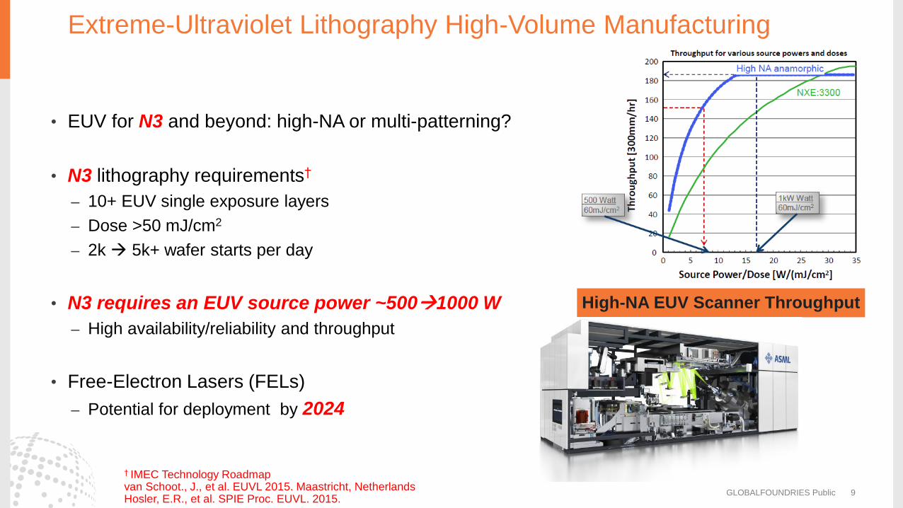
Extreme-Ultraviolet Lithography High-Volume Manufacturing
• EUV for N3 and beyond: high-NA or multi-patterning?
• N3 lithography requirements†
– 10+ EUV single exposure layers
– Dose >50 mJ/cm2
– 2k 5k+ wafer starts per day
• N3 requires an EUV source power ~5001000 W
– High availability/reliability and throughput
• Free-Electron Lasers (FELs)
– Potential for deployment by 2024
† IMEC Technology Roadmap van Schoot., J., et al. EUVL 2015. Maastricht, Netherlands Hosler, E.R., et al. SPIE Proc. EUVL. 2015.
High-NA EUV Scanner Throughput
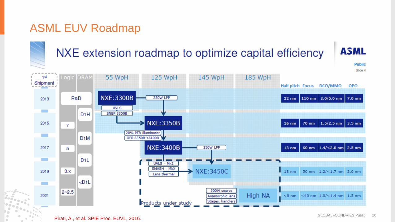
ASML EUV Roadmap
GLOBALFOUNDRIES Public 10 Pirati, A., et al. SPIE Proc. EUVL, 2016.
EUV free-electron laser requirements and considerations for semiconductor manufacturing
GLOBALFOUNDRIES Public 11
Current EUV Lithography Status
Why do we need FELs?
Lithographer’s Perspective on FELs
1
2
3
FEL Research Developments 4
GLOBALFOUNDRIES FEL Research 5
Lithographic Requirements
• An EUV FEL must power multiple scanners simultaneously
• FEL EUV source must operate with an availability of 100%
– Redundancy of high-risk/low-cost machine components
– Minimizing stress on long replacement time components
– Two FELs must be run simultaneously!
• Cost
– FEL EUV program must be substantially cheaper (depreciation + OpEx) and more powerful than an equivalent number of LPP sources to justify development risk
– How many EUVL sources are required for HVM? • 7 nm Logic roadmap from IMEC says 5-10 EUV layers
• 3-4 L/S (>25 mJ/cm2), 2-6 contact (>35 mJ/cm2) = 10x 250 W LPP tools for ~50k wafers/month
• Other: FEL Specific
– Beam Distribution • High power, splitting efficiency
– Power management and Facility Size
• On mask, on mirrors, on wafer, into beam dump, and electrical power
• Integrate with existing fab architecture
– Coherence • Manipulate at scanner or within distribution system?
– Harmonic mitigation scheme • FELs produce a few percent of the fundamental power in higher harmonics
– Wavelength stability? Optical bandwidth? Power stability (Dose repro <0.2%)?
GLOBALFOUNDRIES Public 12
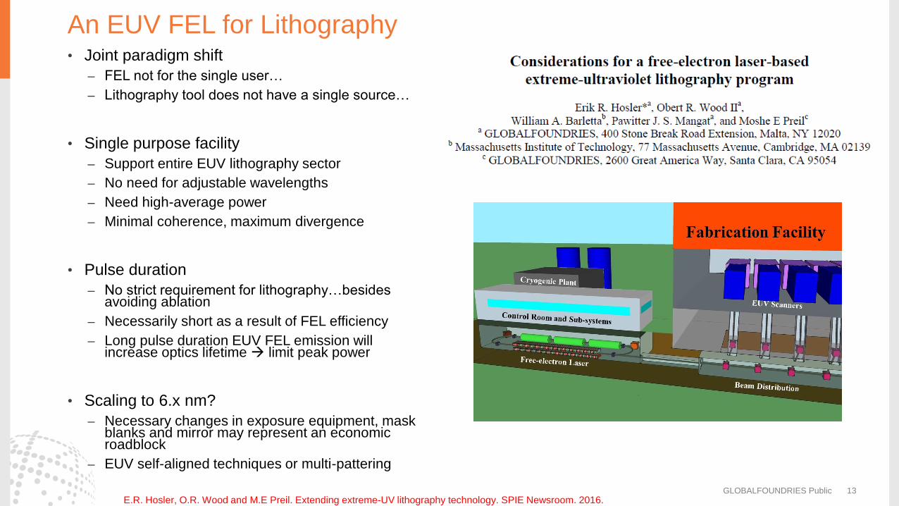
An EUV FEL for Lithography • Joint paradigm shift
– FEL not for the single user…
– Lithography tool does not have a single source…
• Single purpose facility
– Support entire EUV lithography sector
– No need for adjustable wavelengths
– Need high-average power
– Minimal coherence, maximum divergence
• Pulse duration
– No strict requirement for lithography…besides avoiding ablation
– Necessarily short as a result of FEL efficiency
– Long pulse duration EUV FEL emission will increase optics lifetime limit peak power
• Scaling to 6.x nm?
– Necessary changes in exposure equipment, mask blanks and mirror may represent an economic roadblock
– EUV self-aligned techniques or multi-pattering
GLOBALFOUNDRIES Public 13 E.R. Hosler, O.R. Wood and M.E Preil. Extending extreme-UV lithography technology. SPIE Newsroom. 2016.
EUV free-electron laser requirements and considerations for semiconductor manufacturing
GLOBALFOUNDRIES Public 14
Current EUV Lithography Status
Why do we need FELs?
Lithographer’s Perspective on FELs
1
2
3
FEL Research Developments 4
GLOBALFOUNDRIES FEL Research 5
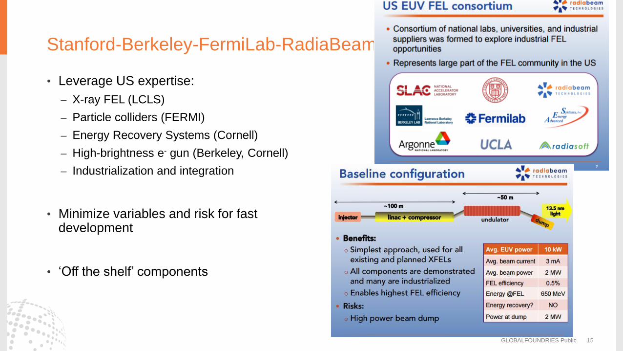
Stanford-Berkeley-FermiLab-RadiaBeam
• Leverage US expertise:
– X-ray FEL (LCLS)
– Particle colliders (FERMI)
– Energy Recovery Systems (Cornell)
– High-brightness e- gun (Berkeley, Cornell)
– Industrialization and integration
• Minimize variables and risk for fast development
• ‘Off the shelf’ components
GLOBALFOUNDRIES Public 15
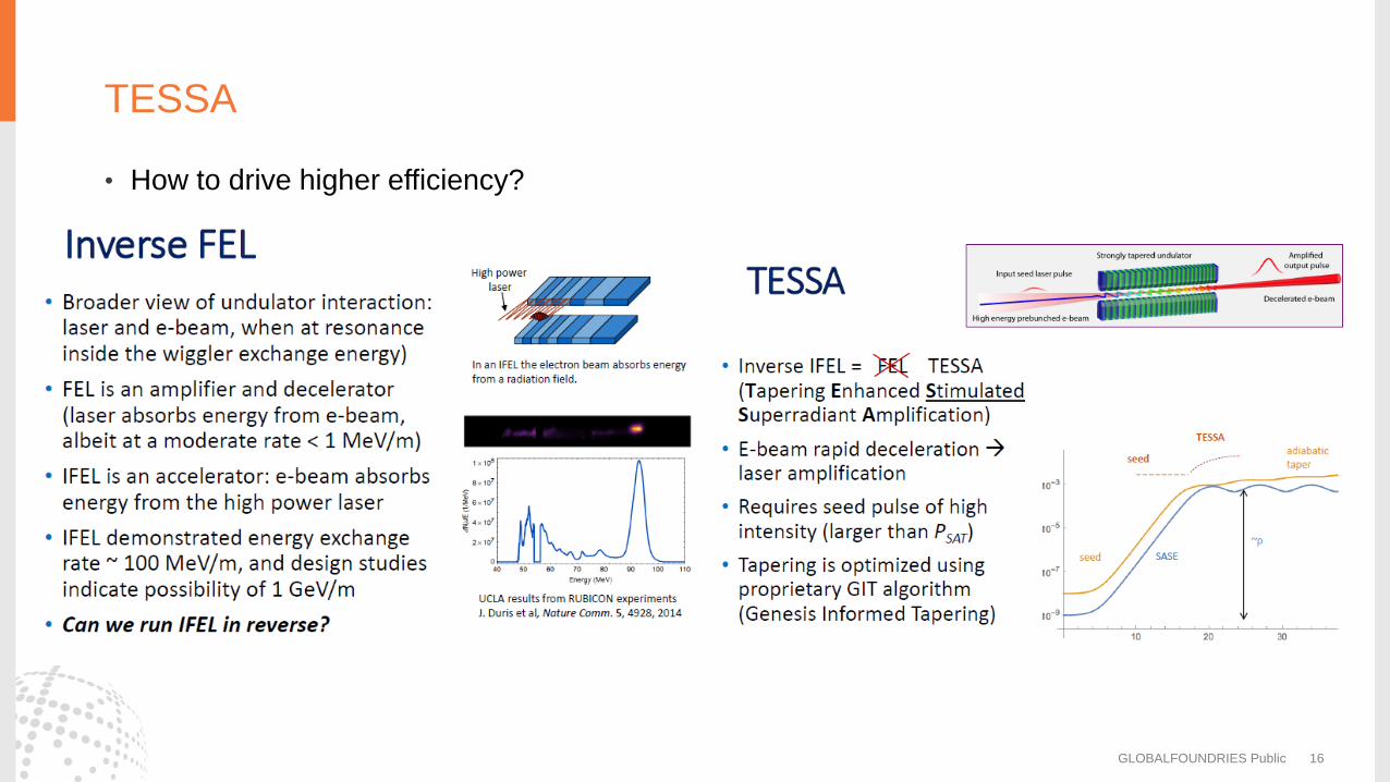
TESSA
• How to drive higher efficiency?
GLOBALFOUNDRIES Public 16
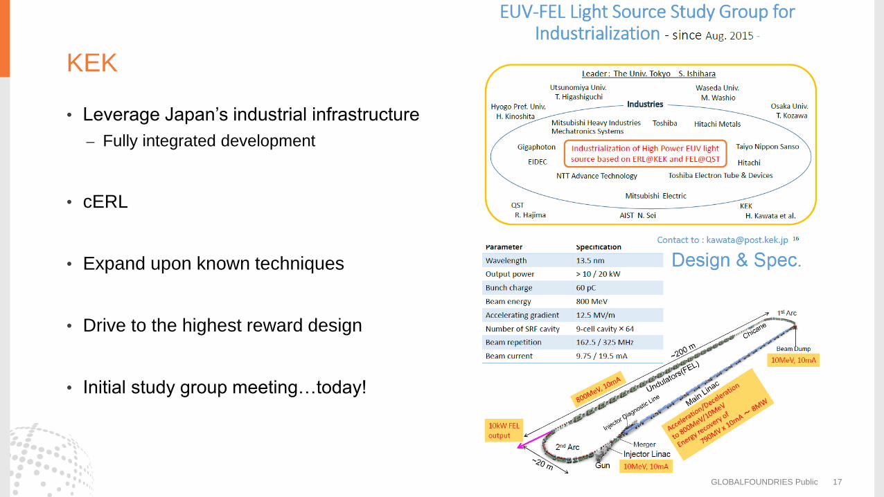
KEK
• Leverage Japan’s industrial infrastructure
– Fully integrated development
• cERL
• Expand upon known techniques
• Drive to the highest reward design
• Initial study group meeting…today!
GLOBALFOUNDRIES Public 17
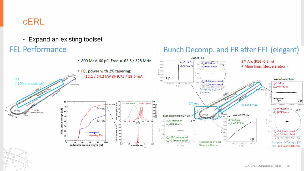
cERL
• Expand an existing toolset
GLOBALFOUNDRIES Public 18
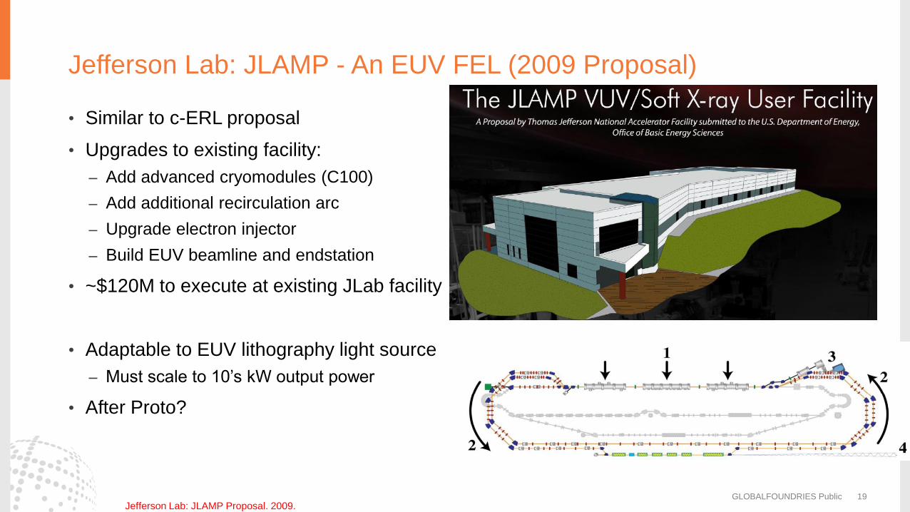
Jefferson Lab: JLAMP - An EUV FEL (2009 Proposal)
• Similar to c-ERL proposal
• Upgrades to existing facility:
– Add advanced cryomodules (C100)
– Add additional recirculation arc
– Upgrade electron injector
– Build EUV beamline and endstation
• ~$120M to execute at existing JLab facility
• Adaptable to EUV lithography light source
– Must scale to 10’s kW output power
• After Proto?
GLOBALFOUNDRIES Public 19 Jefferson Lab: JLAMP Proposal. 2009.
EUV free-electron laser requirements and considerations for semiconductor manufacturing
GLOBALFOUNDRIES Public 20
Current EUV Lithography Status
Why do we need FELs?
Lithographer’s Perspective on FELs
1
2
3
FEL Developments in the US 4
GLOBALFOUNDRIES FEL Research 5
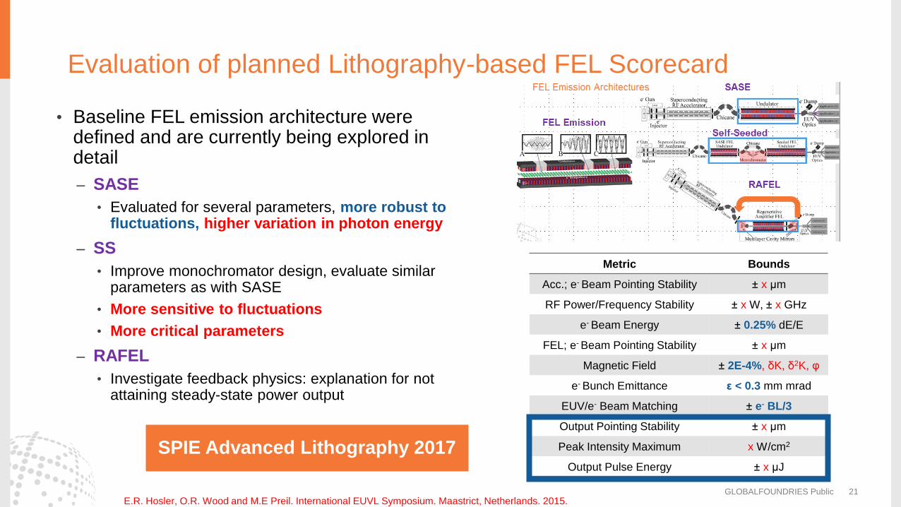
Evaluation of planned Lithography-based FEL Scorecard
• Baseline FEL emission architecture were defined and are currently being explored in detail
– SASE
• Evaluated for several parameters, more robust to fluctuations, higher variation in photon energy
– SS
• Improve monochromator design, evaluate similar parameters as with SASE
• More sensitive to fluctuations
• More critical parameters
– RAFEL
• Investigate feedback physics: explanation for not attaining steady-state power output
Metric Bounds
Acc.; e- Beam Pointing Stability ± x μm
RF Power/Frequency Stability ± x W, ± x GHz
e- Beam Energy ± 0.25% dE/E
FEL; e- Beam Pointing Stability ± x μm
Magnetic Field ± 2E-4%, δK, δ2K, φ
e- Bunch Emittance ε < 0.3 mm mrad
EUV/e- Beam Matching ± e- BL/3
Output Pointing Stability ± x μm
Peak Intensity Maximum x W/cm2
Output Pulse Energy ± x μJ
GLOBALFOUNDRIES Public 21 E.R. Hosler, O.R. Wood and M.E Preil. International EUVL Symposium. Maastrict, Netherlands. 2015.
SPIE Advanced Lithography 2017
Evolutionary Thinking: Research oriented to industrial FELs
• Single user Multi-end stations
• High peak power High average power
• Radiation permits Minimize radiation
• Many applications and extendibility Single purpose and power scaling
• Upgrades and scheduled maintenance blocks predictable, short service
• Constant facility development First Time Right Design
• Value of the science vs. tax dollars Wafer cost
• How many more can we think of…?
GLOBALFOUNDRIES Public 22
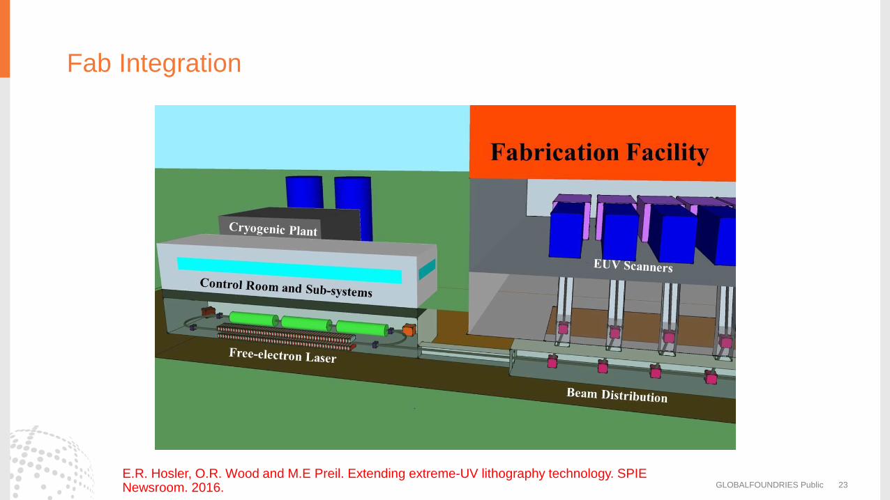
Fab Integration
GLOBALFOUNDRIES Public 23
E.R. Hosler, O.R. Wood and M.E Preil. Extending extreme-UV lithography technology. SPIE Newsroom. 2016.
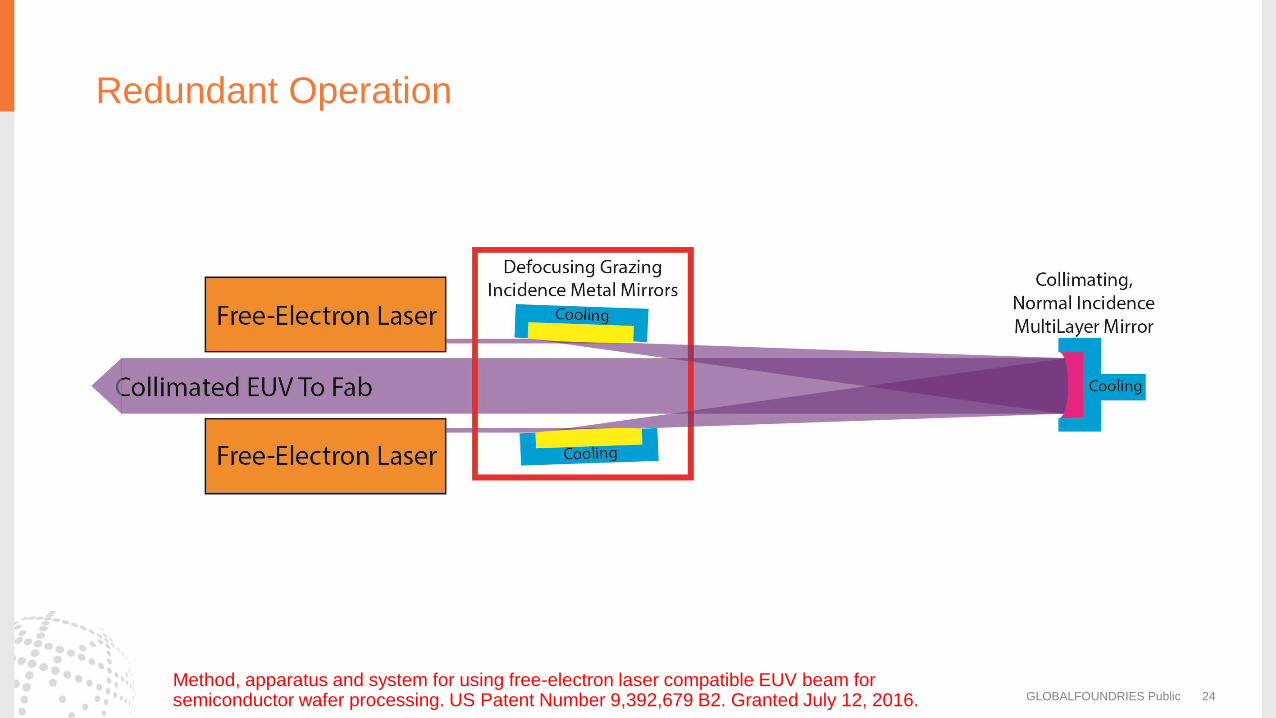
Redundant Operation
GLOBALFOUNDRIES Public 24
Method, apparatus and system for using free-electron laser compatible EUV beam for semiconductor wafer processing. US Patent Number 9,392,679 B2. Granted July 12, 2016.
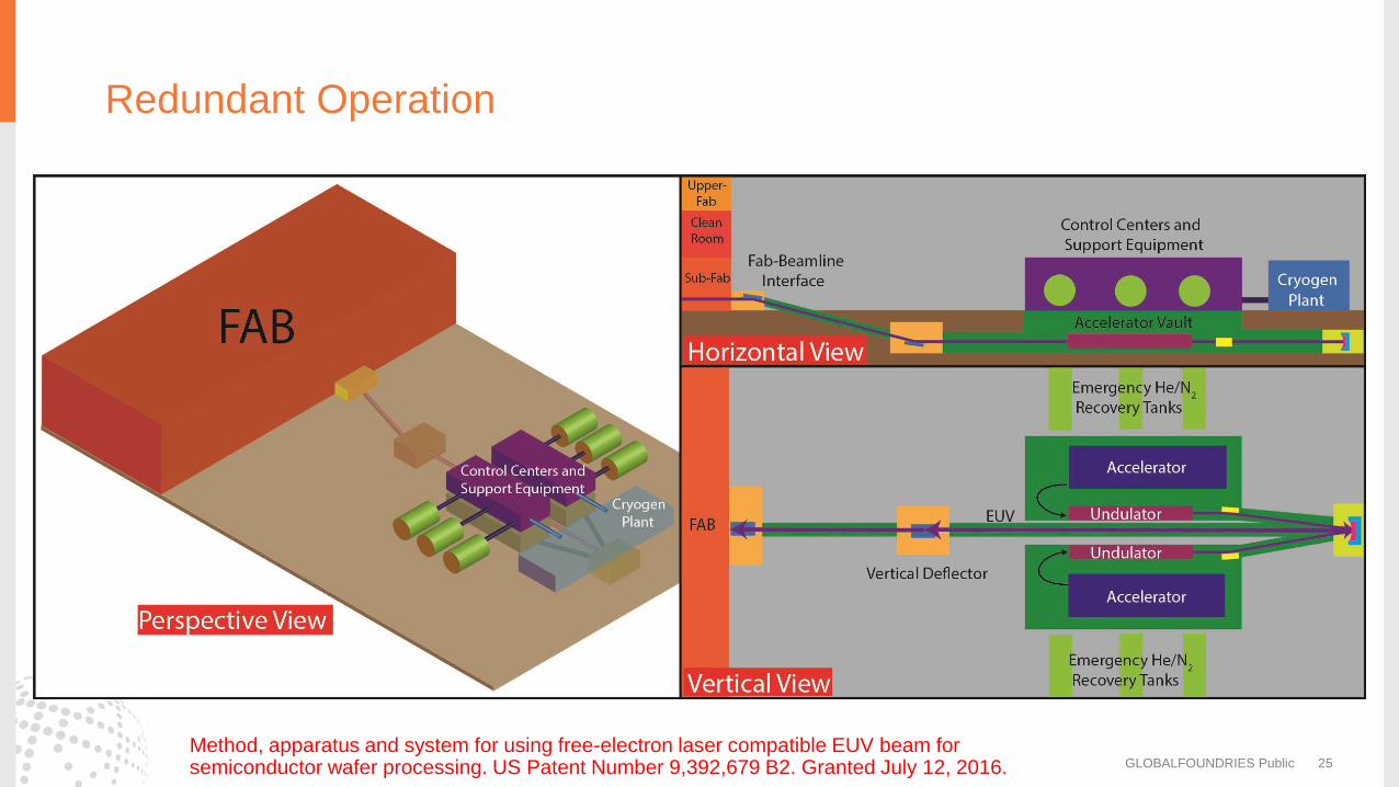
Redundant Operation
GLOBALFOUNDRIES Public 25
Method, apparatus and system for using free-electron laser compatible EUV beam for semiconductor wafer processing. US Patent Number 9,392,679 B2. Granted July 12, 2016.
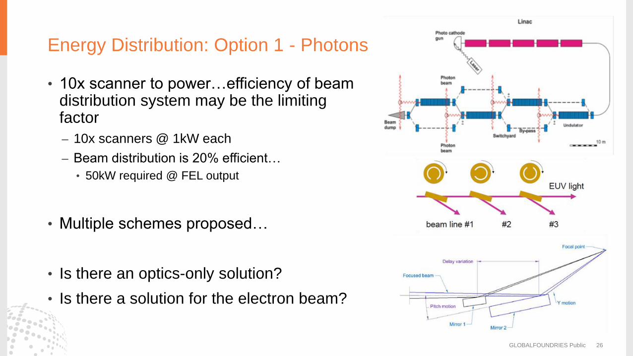
Energy Distribution: Option 1 - Photons
• 10x scanner to power…efficiency of beam distribution system may be the limiting factor
– 10x scanners @ 1kW each
– Beam distribution is 20% efficient…
• 50kW required @ FEL output
• Multiple schemes proposed…
• Is there an optics-only solution?
• Is there a solution for the electron beam?
GLOBALFOUNDRIES Public 26
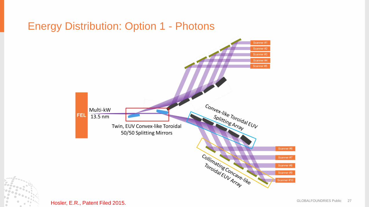
Energy Distribution: Option 1 - Photons
GLOBALFOUNDRIES Public 27 Hosler, E.R., Patent Filed 2015.
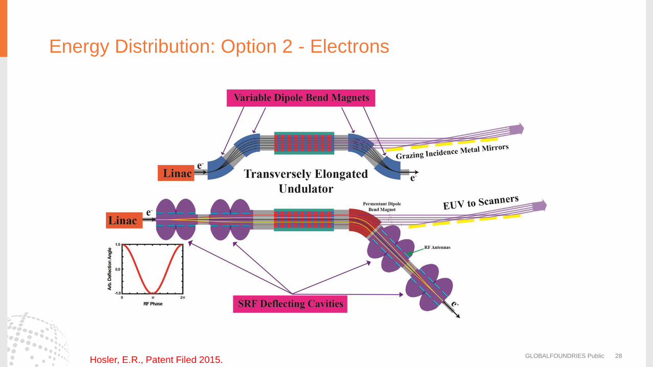
Energy Distribution: Option 2 - Electrons
GLOBALFOUNDRIES Public 28 Hosler, E.R., Patent Filed 2015.
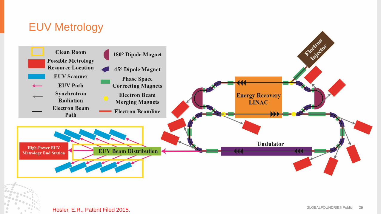
EUV Metrology
GLOBALFOUNDRIES Public 29 Hosler, E.R., Patent Filed 2015.
Summary
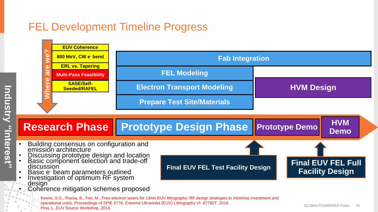
FEL Development Timeline Progress
GLOBALFOUNDRIES Public 31
Ind
us
try C
om
mitm
en
t
Final EUV FEL Test Facility Design Final EUV FEL Full
Facility Design
Prototype Demo
Prepare Test Site/Materials
Research Phase Prototype Design Phase HVM
Demo
Electron Transport Modeling
FEL Modeling
HVM Design
Fab Integration
Wh
ere
are
we?
• Building consensus on configuration and emission architecture
• Discussing prototype design and location • Basic component selection and trade-off
discussion • Basic e- beam parameters outlined • Investigation of optimum RF system
design • Coherence mitigation schemes proposed
800 MeV, CW e- bend
ERL vs. Tapering
Multi-Pass Feasibility
SASE/Self-Seeded/RAFEL
EUV Coherence
Ind
ustry
“In
tere
st”
Keens, S.G., Rossa, B., Frei, M., Free-electron lasers for 13nm EUV lithography: RF design strategies to minimise investment and
operational costs. Proceedings of SPIE 9776, Extreme Ultraviolet (EUV) Lithography VI. 97760T. 2016.
Pina, L. EUV Source Workshop. 2014.
Driving toward an industrial EUV FEL
• Success is two fold dependent
– Development of new technology
– Acceptance
• FEL/Accelerator Paradigm Shift
– Power and availability are king
– Single to many end stations
• Any development program must have a governance body
– Semiconductor manufacturers
– EUV Scanner Supplier(s)
– Accelerator/FEL Research Team
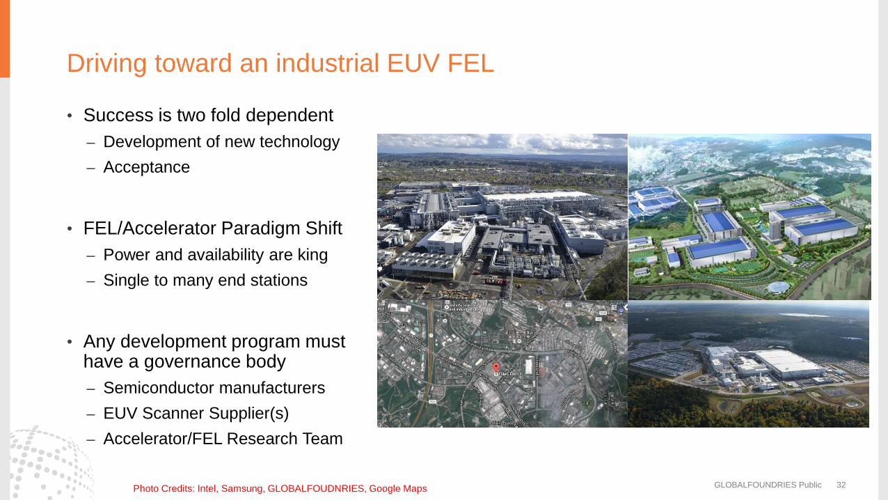
GLOBALFOUNDRIES Public 32 Photo Credits: Intel, Samsung, GLOBALFOUDNRIES, Google Maps