esdemc_pb2014.08 an ethernet cable discharge event (cde) test and measurement system
TRANSCRIPT
An Ethernet Cable Discharge Event (CDE)
Test and Measurement System
Wei Huang, Jerry Tichenor
ESDEMC Technology LLC
Rolla, MO, USA
David Pommerenke, Viswa Pilla, Pratik
Maheshwari, Giorgi Maghlakelidze
Electromagnetic Compatibility Laboratory, Missouri S&T
Rolla, MO, USA
Abstract— A Cable Discharge Event (CDE) is an electrostatic
discharge between a cable and a connector. CDEs occur on
unshielded Ethernet based communication interfaces and inject
currents into the pins directly [1-3]. The charging processes are in
general understood; however, the discharge processes are
complicated due to the number of pins involved and their
connections to a system. Based on an understanding of the factors
which determine the severity of a CDE, this article describes how
to setup a variety of repeatable CDE tests and how to analyze the
measurement results.
Keywords— Cable Discharge Event (CDE) Test; Cable ESD;
I. INTRODUCTION
Both occurrence rate and severity of a CDE needs to be
considered when determining the importance of dedicated CDE
tests to ensure a reliable system. The occurrence rate of a CDE
depends on the type of connector used and the environment the
system is used. While a USB connector on a laptop will receive
many more ESD events than a LAN connector, the LAN
connector still poses a larger risk to the system as it is usually
not shielded and often used in applications that require high
reliability such as back bone internet routers. In contrast to a
USB connector, a LAN connector can have a spark from the
connector to a pin during a CDE. In the case of USB connectors
the connector shells will mate first. Provided that the shells are
connected to the shield and to the system ground, most of the
discharge current will flow on the connector shells.
For the LAN CDE case a good understanding of the
dominating processes provides a mean for developing and
validating models. These models will allow computer
simulation, and laboratory test setup formulation for
reproducing real CDEs. This is crucial for IC and system level
engineers to study and optimize the immunity of Ethernet based
communications interface designs.
It is well known that triboelectric charging is the culprit that
generates the charge on a cable [1],[2]. This fact is especially
important in Ethernet communication systems due to the long
lengths of UPT cable that must be pulled through conduit,
which may result into large charges. A model for describing the
interaction of one twisted pair in a UTP (Unshielded Twisted
Pair) cable is presented in [2] using a three body model
analyzed from an electrostatic point of view. In [3] a system for
discharging a cable using a relay on a test bed is presented, and
experimental results are shown. In regards to the measurement
analysis side of Ethernet CDE, there are few publications
discussing the phenomena. Some ESD test setup have been
developed to repeat ESD current transfer through Ethernet
magnetic effects in [4] and [5].
The focus of this article is to present a CDE testing system
that will allow for real world test conditions to be reproduced
in the laboratory, thereby providing design engineers a quick
and reliable method for testing new hardware designs. The test
system will allow for different types of copper based Ethernet
cables, and twisted pair termination strategies. Further, full
control of the charge and discharge sequence of each cable line
allows for all possible cases to be explored.
II. IMPORTANT PARAMETERS IN ETHERNET CDE
Prior to discussing the CDE test system, a few important
parameters of copper based Ethernet cable CDE, especially
UTP must be reviewed.
A. Parameters of the charged Ethernet cable affecting CDE
Several important parameters must be considered in UTP
cables. The first parameter is the charging processes in UTP
cables. In particular, the wires can be charged due to charges
on the outside of the jacket, due to migration of charges through
the jacket and insulation to the wires, or due to direct contact of
the wires with a charged object. The voltage magnitude can be
as high as 2 kV. In most cases all wires will be charged to the
same voltage. If the spatial arrangement of the cables is
changed, the capacitance between the charged wires and
ground will also change, which can further increase the charge
voltage.
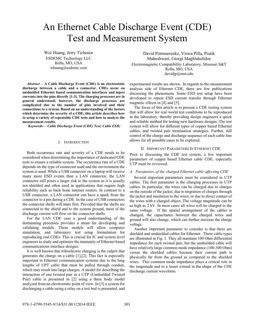
Another important parameter to consider is that there are
shielded and unshielded cables for Ethernet. These cable types
are illustrated in Fig. 1. They all maintain 100 Ohm differential
impedance for each twisted pair, but the unshielded cable will
have relatively large common mode impedance (100-300 Ohm)
versus the shielded cables because their current path is
physically far from the ground as compared to the shielded
wires. This common mode impedance plays a critical role in
the magnitude and to a lesser extend in the shape of the CDE
discharge current waveform.
978-1-4799-5545-9/14/$31.00 ©2014 IEEE 301
Fig 1. Different shielding types of Ethernet cables
B. The termination of the Ethernet device
Load terminations also play an important role in the
characterization of a CDE. Many different types of termination
schemes exist, however, the most commonly used is the Bob
Smith Termination [5]. This termination uses a 75 resistor
for a common mode impedance match at each signal pair, and
they all connect via a high voltage capacitor to chassis ground
as shown in Fig 2. The isolation between the Ethernet
connector/chassis and internal PHY circuit is established
through a transformer and some designs incorporate common
mode chokes to further reduce common mode current
motivated EMI concerns. Further variations of the Bob Smith
circuit can be found in power over Ethernet applications, and
strongly cost reduced designs.
Fig 2. Typical termination of Ethernet device.
One pin will make the first contact and any other pin will
contact next. The initial contact leads to a charge redistribution,
a partial discharge of the total charge on the cable, and it can
charge the capacitor used in the Bob Smith circuit. Depending
on the contact sequence, various common mode and differential
mode termination plus the PHY IC circuit determine the load
of the discharge current path and therefore are the important
factors that determine the CDE current waveform.
C. The ESD events during CDE
The Ethernet cable connection includes several metal to
metal contacts, which can lead to multiple ESD events during
connection. For the case of plugging a shielded Ethernet cable
into a shielded Ethernet connector, the first ESD event is the
discharge between the shielding of the cable to the shielding of
Ethernet connector as this is the first contact point. Normally
this ESD is not likely to cause any failures if the DUT is
shielded. For the case of an unshielded cable or an unshielded
Ethernet connector the current must flow in the wires of the
UTP.
When an Ethernet cable is plugged into a connector, many
possible contact sequences can occur. Theoretically there could
be eight separate ESD events, one for each pin. However, each
contact will minimize the voltage between the other pins and
the connector.
This is caused by the large mutual capacitance between the
wires, and by charging the Bob Smith Termination.
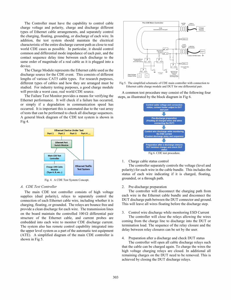
To illustrate the charging of the capacitor in the Bob Smith
circuit, a 100 m long shielded cable was charged to 100 V
between the shield and its wires and inserted into an Ethernet
device. A result from this experiment is shown in Fig 3.
Because the capacitance between the wires and the shield is
much larger than the 1000 pF capacitor, the voltage reaches
over 90 V immediately after first contact, thereby lowering the
voltage difference between other connecting pins. For the next
seven contact events the voltage difference across the contacts
is drastically reduced..
The voltage waveform shown in Fig 3 gradually diminishes
due to the 100 M resistive voltage probe used in the
measurement. Without this drain path the voltage on the cable
will remain high for a very long time after the connection is
made. If the other end of this cable is plugged into an Ethernet
device another cable discharge event may occur.
Fig 3. Voltage across the 1 nF HV capacitor in the Bob Smith termination
during CDE.
Because the differential pairs of the cable have a well-
defined 100 discharge impedance, after the first wire has
made contact and the high voltage capacitor has a low
impedance path to ground, such that the second wire also
experiences the discharge as it is making contact, resulting in a
differential ESD event. This differential ESD current can easily
transfer through the magnetics to the isolated PHY circuit,
which is hazardous for the PHY chip.
III. THE ETHERNET CDE TEST SYSTEM CONCEPT
A good Ethernet CDE test setup should be able to control as
many of the parameters related to the cable discharge event as
possible, and provide a repeatable test. To do this the setup
must have these three main components; a Controller, a Charge
Module, and a Failure Test Monitor.
302
The Controller must have the capability to control cable
charge voltage and polarity, charge and discharge different
types of Ethernet cable arrangements, and separately control
the charging, floating, grounding, or discharge of each wire. In
addition, the test system should maintain the electrical
characteristic of the entire discharge current path as close to real
world CDE cases as possible. In particular, it should control
common and differential mode impedance of each pair, and the
contact sequence delay time between each discharge to the
same order of magnitude of a real cable as it is plugged into a
device.
The Charge Module represents the Ethernet cable used as the
discharge source for the CDE event. This consists of different
lengths of various CAT5 cable types. For research purposes,
different types of cables and how they are arranged must be
studied. For industry testing purposes, a good charge module
will provide a worst case, real world CDE source.
The Failure Test Monitor provides a means for verifying the
Ethernet performance. It will check if a failure has occurred,
or simply if a degradation in communication speed has
occurred. It is important this is automated due to the vast array
of tests that can be performed to check all discharge sequences.
A general block diagram of the CDE test system is shown in
Fig 4.
Fig. 4. A CDE Test System Concept.
A. CDE Test Controller
The main CDE test controller consists of high voltage
supplies (dual polarity), relays to separately control the
connection of each Ethernet cable wire, including whether it is
charging, floating, or grounded. The relays are bounce free and
provide a clean discharge for each wire. The transmission lines
on the board maintain the controlled 100 differential pair
structure of the Ethernet cable, and current probes are
embedded into each wire to monitor CDE discharge current.
The system also has remote control capability integrated into
the upper level system as a part of the automatic test equipment
(ATE). A simplified diagram of the main CDE controller is
shown in Fig 5.
HV+ HV-High VoltageSupply Relay
SMA I 1
DischargeRelays
Charging RelaysSwitch HV or
Ground/Floating
PCBtransmission line pair
1 of 4twistedpairs
LAN InConnector
LAN OutConnector
1 meter CAT5E Cable
DUT
ChargeModule
Current P robe5 V/A
SMA I 2
CAT5EUTP
DUT HV Cap Discharge
Relay 8 wires share 1discharge path
DIP Switchto GND
The CDE Main Controller
Fig 5. The simplified schematic of CDE main controller with connection to
Ethernet cable charge module and DUT for one differential pair.
A common test procedure may consist of the following four
steps, as illustrated by the block diagram in Fig 6.
Fig 6. CDE test procedure.
1. Charge cable status control
The controller separately controls the voltage (level and
polarity) for each wire in the cable bundle. This includes the
status of each wire indicating if it is charged, floating,
grounded, or a through path.
2. Pre-discharge preparation
The controller will disconnect the charging path from
each wire in the Ethernet cable bundle and disconnect the
DUT discharge path between the DUT connector and ground.
This will leave all wires floating before the discharge step.
3. Control wire discharge while monitoring ESD Current
The controller will close the relays allowing the wires
coming from the charge line to discharge into the DUT or
termination load. The sequence of the relay closure and the
delay between relay closures can be set by the user.
4. Preparation after a discharge and check DUT status
The controller will open all cable discharge relays such
that the cable can be charged again. To charge the wires the
high voltage charging relays are closed. In additional all
remaining charges on the DUT need to be removed. This is
achieved by closing the DUT discharge relays.
303
The controller will open all cable discharge relays, then
close all high voltage charging relays and DUT connector
discharge relays to prepare for next CDE test.
B. Charge Module
In real world Ethernet cable installations there are many
different possibilities in regard to cable type and arrangements,
leading to unlimited test scenarios. Some common real world
arrangements are:
A. Cable hanging on the celling (relatively far from ground)
B. Cable on the floor (very close to the ground)
C. A spool of new cable
D. Cable pulled through conduit (very close to the ground)
Fig 7. A rack mount 200 meters of UTP cable Charge Module.
C. Failure Test Module
Besides the setup for CDE test control, it is also important to
test for normal Ethernet performance and functionality. It is
important to understand the effects of applied CDE on the DUT,
and as in the block diagram of Fig 4, an Ethernet traffic test
system should not only monitor the status of DUT during CDE
test, but also check the performance of the CDE applied ported
after each test level.
D. Calibration of the Ethernet CDE Test System
A CDE Tester (Model ES631-LAN) with two different types
of Ethernet Charge Modules (shielded and unshielded) was
built. The analysis of real discharge waveforms is difficult. For
that reason a proper calibration method with well-defined test
loads is important to verify the functionality, to understand the
current paths and the output parameters of the CDE test setup.
A set of calibration loads including short, open, and 100
differential load were built using 10 cm CAT5E UTP cables,
and are shown in Fig 8.
Fig 8. CDE calibration loads: short, open, and 100 differential termination
The EIA 568B cable standard was used for all Ethernet
wiring, Fig 9.
Fig 9. EIA 568B Ethernet Wiring Standard.
In the measurement setup the oscilloscope was set to capture
the waveforms: Channel 1-voltage on line 5, Channel 2-current
on line 5, Channel 3-voltage on line 4, and Channel 4-current
on line 4. The voltage probes were 1010:1 (5 k/50 resistor
bridge = 101:1, plus 20 dB attenuator). And the current probes
were 20:1 (5 V/A plus 40 dB attenuator). The CDE Controller
in all tests was set to 500 V, and depending on the test
configuration the Charge Module and DUT may have been
grounded.
Setup 1 consisted of a short connected to CDE Controller
output, one differential pair with one side grounded and pre-
connected to the load, and a 100 meter Charge Module using
S/UTP cable with the chassis not grounded. The setup and
measurement waveforms are shown in Fig 10. From the
simplified circuit, after the relay is closed in line 5, we expect
a large current flowing from line 5 to line 4 over the differential
100 transmission line structure and the peak current should
be 5 A (500 V/100 ). From the waveforms it can be
confirmed that the current waveform starts with 5 A peak.
Then the waveform shows significant cable loss as the
waveforms rapidly decay. After the current reaches the cable
ends, reflections occur due to mismatches and several
reflections happen until the total signal approaches zero. The
voltage is a RC discharge waveform through the voltage
measurement path.
Fig 10. Simplified schematic and waveforms of CDE calibration setup 1.
Setup 2 is similar to setup 1 except the charge module chassis
is connected to ground. The setup and measurement waveforms
are shown in Fig 11. As can be seen, the current waveforms
are the same as the first setup, but the voltage waveform RC
304
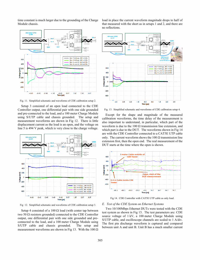
time constant is much larger due to the grounding of the Charge
Module chassis.
Fig. 11. Simplified schematic and waveforms of CDE calibration setup 2.
Setup 3 consisted of an open load connected to the CDE
Controller output, one differential pair with one side grounded
and pre-connected to the load, and a 100 meter Charge Module
using S/UTP cable and chassis grounded. The setup and
measurement waveforms are shown in Fig 12. There is little
displacement current as the load is an open, and the voltage on
line 5 is 494 V peak, which is very close to the charge voltage.
Fig 12. Simplified schematic and waveforms of CDE calibration setup 3.
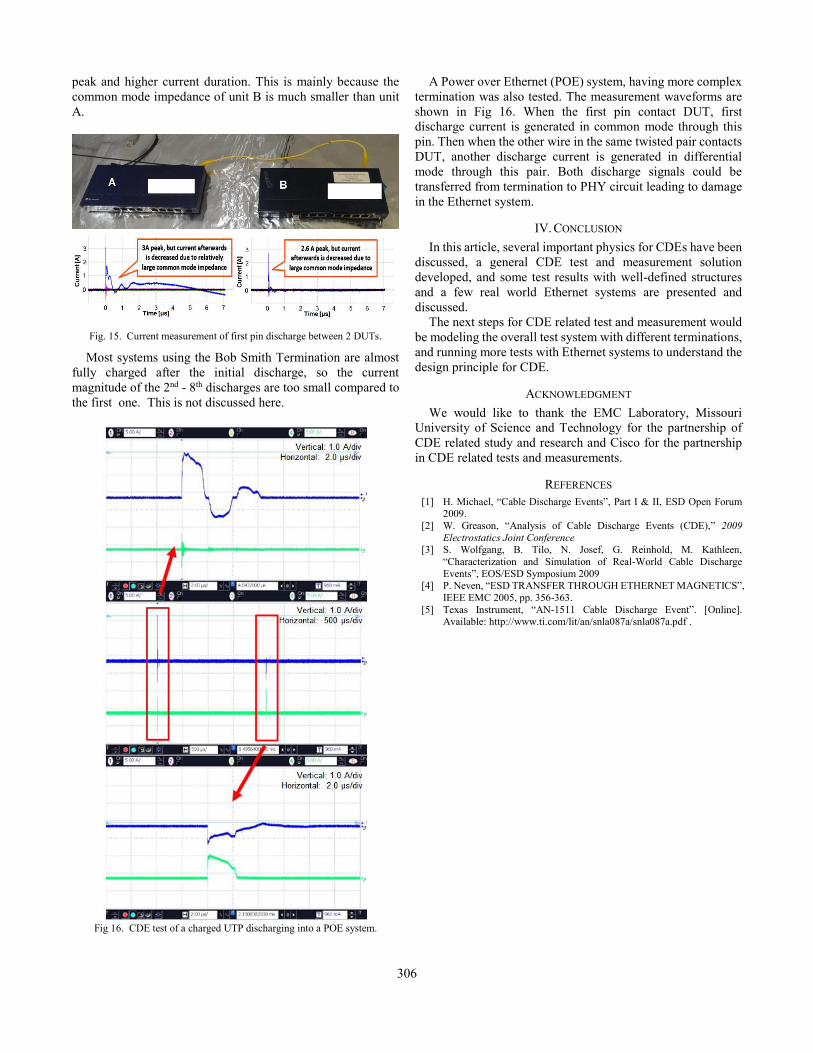
Setup 4 consisted of a 100 load (with center tap between
two 50 resistors grounded) connected to the CDE Controller
output, one differential pair with one side grounded and pre-
connected to the load, and a 100 meter Charge Module using
S/UTP cable and chassis grounded. The setup and
measurement waveforms are shown in Fig 13. With the 100
load in place the current waveform magnitude drops to half of
that measured with the short as in setups 1 and 2, and there are
no reflections.
Fig. 13. Simplified schematic and waveforms of CDE calibration setup 4.
Except for the shape and magnitude of the measured
calibration waveforms, the time delay of the measurement is
also important to understand, in particular, which part of the
waveform is due to the 100 transmission line extension, and
which part is due to the DUT. The waveforms shown in Fig 14
are with the CDE Controller connected to a CAT5E UTP cable
only. The current waveform shows the 100 transmission line
extension first, then the open end. The real measurement of the
DUT starts at the time where the open is shown.
Fig 14. CDE Controller with CAT5E UTP cable as only load.
E. Test of the CDE System on Ethernet Systems
Two 10/100Mbps Ethernet DUTs were tested with the CDE
test system as shown in Fig 15. The test parameters are: CDE
source voltage of 1 kV, a 100 meter Charge Module using
S/UTP cable, and oscilloscope channels are scaled to 1 A/div.
The first pin discharge waveform is captured and compared
between unit A and unit B. Unit B has a much smaller current
305
peak and higher current duration. This is mainly because the
common mode impedance of unit B is much smaller than unit
A.
Fig. 15. Current measurement of first pin discharge between 2 DUTs.
Most systems using the Bob Smith Termination are almost
fully charged after the initial discharge, so the current
magnitude of the 2nd - 8th discharges are too small compared to
the first one. This is not discussed here.
Fig 16. CDE test of a charged UTP discharging into a POE system.
A Power over Ethernet (POE) system, having more complex
termination was also tested. The measurement waveforms are
shown in Fig 16. When the first pin contact DUT, first
discharge current is generated in common mode through this
pin. Then when the other wire in the same twisted pair contacts
DUT, another discharge current is generated in differential
mode through this pair. Both discharge signals could be
transferred from termination to PHY circuit leading to damage
in the Ethernet system.
IV. CONCLUSION
In this article, several important physics for CDEs have been
discussed, a general CDE test and measurement solution
developed, and some test results with well-defined structures
and a few real world Ethernet systems are presented and
discussed.
The next steps for CDE related test and measurement would
be modeling the overall test system with different terminations,
and running more tests with Ethernet systems to understand the
design principle for CDE.
ACKNOWLEDGMENT
We would like to thank the EMC Laboratory, Missouri
University of Science and Technology for the partnership of
CDE related study and research and Cisco for the partnership
in CDE related tests and measurements.
REFERENCES
[1] H. Michael, “Cable Discharge Events”, Part I & II, ESD Open Forum 2009.
[2] W. Greason, “Analysis of Cable Discharge Events (CDE),” 2009
Electrostatics Joint Conference [3] S. Wolfgang, B. Tilo, N. Josef, G. Reinhold, M. Kathleen,
“Characterization and Simulation of Real-World Cable Discharge
Events”, EOS/ESD Symposium 2009 [4] P. Neven, “ESD TRANSFER THROUGH ETHERNET MAGNETICS”,
IEEE EMC 2005, pp. 356-363.
[5] Texas Instrument, “AN-1511 Cable Discharge Event”. [Online]. Available: http://www.ti.com/lit/an/snla087a/snla087a.pdf .
306