equivalent circuits for multiconductor microstrip bend discontinuities
TRANSCRIPT

62 IEEE TRANSACTIONS ON MICROWAVE THEORY AND TECHNIQUES, VOL. 41, NO. I , JANUARY 1993
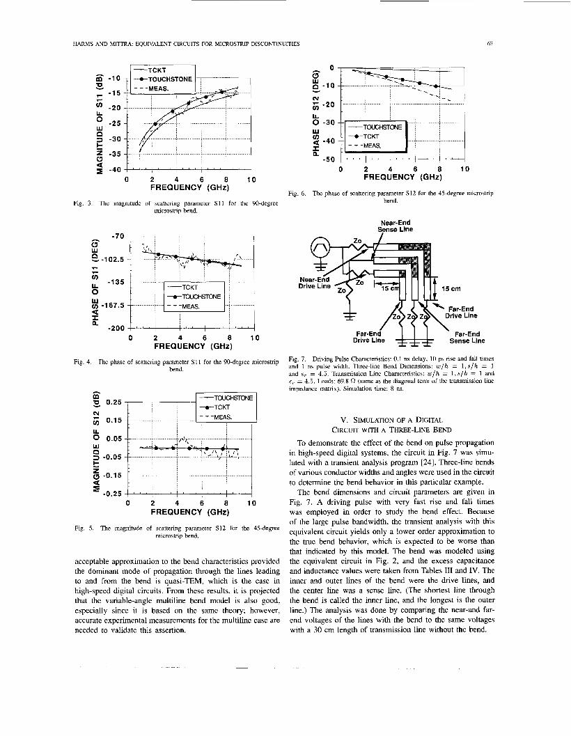
Equivalent Circuits for Multiconductor Microstrip Bend Discontinuities
Paul H. Harms, Member, IEEE, and Raj Mittra, Fellow, IEEE
Abstract-With the increasing density of digital circuit layouts and faster pulse edges, microstrip discontinuities, e.g., bends, that were previously considered insignificant have now been shown to introduce noticeable signal degradation for short risetime pulses. In this paper, the T-equivalent circuit previously used for single-line microstrip bends is extended to the variable-angle, multiconductor microstrip bend. A brief overview is given of the excess-charge and current approaches which are employed to obtain the capacitance and inductance matrices for the equivalent circuit. These techniques effectively avoid the majority of numer- ical difficulties that occur in accounting for the infinite extent of the microstrip lines making up bends with arbitrary bend angles. In addition, to accurately accommodate the oblique bend angles without requiring many unknowns, the charge and current distributions are modeled with a combination of rectangular and triangular patches. Comparisons with previously published results from the technical literature and with experimental data are used to validate the excess capacitance and inductance compu- tations. The excess capacitance and inductance matrices of several
the bend in its microstrip environment; the measurements are relatively easy to perform with the accurate TRL calibration technique for network analyzers [21]. On the other hand, the resonance measurements and associated analyses are more difficult to make for the microstrip bends, especially since the capacitive and inductive values of microstrip bends are very small. Furthermore, these measurements are more suitable for extracting the excess capacitance and inductance of the bend than for examining the dynamic behavior of the model which is needed for determining the accuracy of the model at characterizing the bend discontinuity.
The multiline bend and its corresponding equivalent circuit are shown in Figs. 1 and 2. This model is an extension of the T-equivalent circuit used for single-line bends [l], [2]. It assumes that the propagation through the microstrips leading to and from the bend is quasi-TEM and that the phase difference
three-line bends are presented, and the three-line bend model is used in a simulation of a high-speed digital circuit to demonstrate the effect of the bend on digital pulse waveforms.
due to the bend is negligible so that the effect of the bend can be accurately accounted for by lumped inductive and capacitive elements. Radiation, conduction and dielectric
I. INTRODUCTION
ITH THE advent of faster digital systems, CAD pack- ages must be able to model electromagnetic phenom-
ena such as pulse dispersion, losses, crosstalk and the presence of discontinuities in transmission lines in order to be a useful design tool. One area of interest is in developing lumped and frequency-dependent equivalent circuits for discontinuity effects, which can then be easily added to a CAD system [l], [2]. Much attention has been devoted to the analysis of various microstrip discontinuities [ 11-[20], such as slots, gaps, steps, vias, the single-line bend, coupled right-angle bend, and microstrip T junctions, just to name a few. How- ever, to date, the variable-angle multiline bend, which occurs quite frequently in the PC board designs, has not been fully analyzed. This paper presents a quasistatic analysis of the multiline microstrip bend discontinuity with arbitrary angle and employs the excess inductance and capacitance matrices in a lumped equivalent circuit model for the discontinuity. A thorough study of the model is presented which includes a scattering parameter analysis of the equivalent circuit as opposed to the resonance measurements made in the past [9], [12]. The scattering parameter approach was chosen because it provides information on the dynamic behavior of
Manuscript received January 28, 1992; revised April 21, 1992.
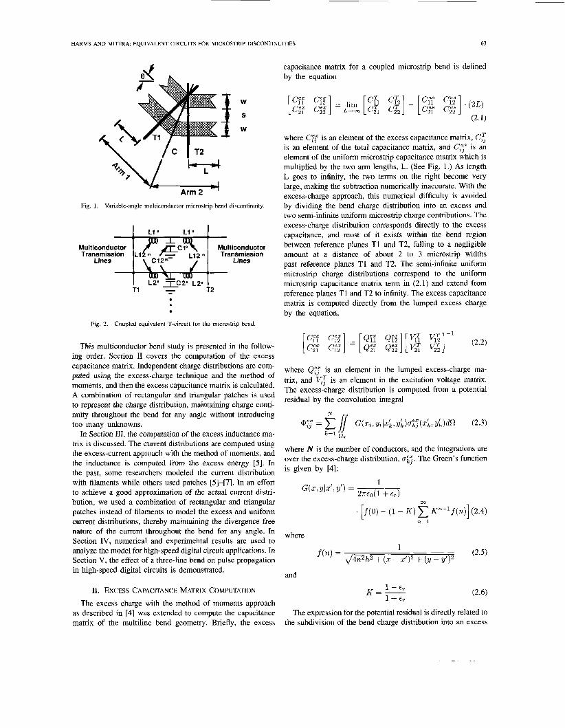
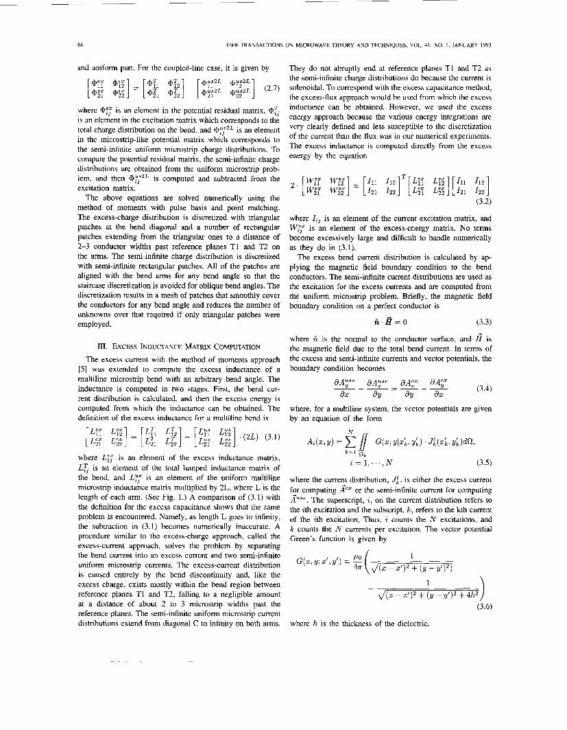
losses of the bend and connecting microstrips are also assumed to be negligible. One T-circuit is used for the bend in each line, with the mutual coupling taken care of by the mutual excess capacitance and inductance. For an N-line bend, the equivalent circuit parameters are related to the coefficients of capacitance and the coefficients of inductance for the bend discontinuity by the equations L1" = L11/2, L12" = L12/2, CIS = C11 + C12 + C13 + . . . + ClN, C12" = -C12, etc. where Lij and Cij are terms in the coefficient matrices. The microstrip lines outside reference planes T1 and T2, shown in Fig. 1, are modeled using multiconductor transmission lines as shown in Fig. 2. The model assumes quasi-TEM propagation up to reference planes T1 and T2 even though the actual propagation is no longer quasi-TEM at this point.
Both of the reactive elements, i.e., the inductance and capacitance of the bend discontinuity, have to be computed separately because the propagation through the bend is not TEM. Of the various techniques that have been applied to compute the inductance and capacitance of microstrip dis- continuities [I], [2], the excess-charge approach developed by Silvester and Benedek [3], [4] and the excess-current approach developed by Gopinath and Easter [5] were employed in this work because these methods effectively account for the infinite extent of the microstrips making up the bend. (See Fig. 1) With the excess charge/current approach, one deals with the
The authors are with the -Electromagnetic Communication Laboratory, Department of Electrical and Computer Engineering, University of Illinois, 1406 W. Green St., Urbana, IL 61801-2991.
quantities directly, which provides one with an accurate and simple means for truncating the microstrip arms without
IEEE Log Number 9204029. sacrificing the accuracy of computation.
0018-9480/93$03.00 0 1993 IEEE
HARMS AND MIlTRA: EQUIVALENT CIRCUITS FOR MICROSTRIP DISCONTINUITIES 63
W
S f W
Fig. 1. Variable-angle multiconductor microstrip bend discontinuity.
L1 L1'
Multiconductor ~ 1 2 m Transmission
Lines
L2' T C 2 ' L2" T1 - T2 - .
Fig. 2. Coupled equivalent T-circuit for the microstrip bend.
This multiconductor bend study is presented in the follow- ing order. Section I1 covers the computation of the excess capacitance matrix. Independent charge distributions are com- puted using the excess-charge technique and the method of moments, and then the excess capacitance matrix is calculated. A combination of rectangular and triangular patches is used to represent the charge distribution, maintaining charge conti- nuity throughout the bend for any angle without introducing too many unknowns.
In Section 111, the computation of the excess inductance ma- trix is discussed. The current distributions are computed using the excess-current approach with the method of moments, and the inductance is computed from the excess energy [5 ] . In the past, some researchers modeled the current distribution with filaments while others used patches [5]-[7]. In an effort to achieve a good approximation of the actual current distri- bution, we used a combination of rectangular and triangular patches instead of filaments to model the excess and uniform current distributions, thereby maintaining the divergence free nature of the current throughout the bend for any angle. In Section IV, numerical and experimental results are used to analyze the model for high-speed digital circuit applications. In Section V, the effect of a three-line bend on pulse propagation in high-speed digital circuits is demonstrated.
11. EXCESS CAPACITANCE MATRIX COMPUTATION
The excess charge with the method of moments approach as described in [4] was extended to compute the capacitance matrix of the multiline bend geometry. Briefly, the excess
capacitance matrix for a coupled microstrip bend is defined by the equation
where is an element of the excess capacitance matrix, (7: is an element of the total capacitance matrix, and C y is an element of the uniform microstrip capacitance matrix which is multiplied by the two arm lengths, L. (See Fig. 1.) As length L goes to infinity, the two terms on the right become very large, making the subtraction numerically inaccurate. With the excess-charge approach, this numerical difficulty is avoided by dividing the bend charge distribution into an excess and two semi-infinite uniform microstrip charge contributions. The excess-charge distribution corresponds directly to the excess capacitance, and most of it exists within the bend region between reference planes T1 and T2, falling to a negligible amount at a distance of about 2 to 3 microstrip widths past reference planes T1 and T2. The semi-infinite uniform microstrip charge distributions correspond to the uniform microstrip capacitance matrix term in (2.1) and extend from reference planes TI and T2 to infinity. The excess capacitance matrix is computed directly from the lumped excess charge by the equation,
where Q:; is an element in the lumped excess-charge ma- trix, and is an element in the excitation voltage matrix. The excess-charge distribution is computed from a potential residual by the convolution integral
where N is the number of conductors, and the integrations are over the excess-charge distribution, C T : ~ . The Green's function is given by [4]:
n=l
where
and 1 - E , Kz- 1 + ET
The expression for the potential residual is directly related to the subdivision of the bend charge distribution into an excess
64 IEEE TRANSACTlONS ON MICROWAVE THEORY AND TECHNIQUES, VOL. 41, NO. I , JANUARY 1993
and uniform part. For the coupled-line case, it is given by
where is an element in the potential residual matrix, @; is an element in the excitation matrix which corresponds to the total charge distribution on the bend, and @y2L is an element in the microstrip-like potential matrix which corresponds to the semi-infinite uniform microstrip charge distributions. To compute the potential residual matrix, the semi-infinite charge distributions are obtained from the uniform microstrip prob- lem, and then @y2’ is computed and subtracted from the excitation matrix.
The above equations are solved numerically using the method of moments with pulse basis and point matching. The excess-charge distribution is discretized with triangular patches at the bend diagonal and a number of rectangular patches extending from the triangular ones to a distance of 2-3 conductor widths past reference planes T1 and T2 on the arms. The semi-infinite charge distribution is discretized with semi-infinite rectangular patches. All of the patches are aligned with the bend arms for any bend angle so that the staircase discretization is avoided for oblique bend angles. The discretization results in a mesh of patches that smoothly cover the conductors for any bend angle and reduces the number of unknowns over that required if only triangular patches were employed.
111. EXCESS INDUCTANCE MATRIX COMPUTATION
The excess current with the method of moments approach [5] was extended to compute the excess inductance of a multiline microstrip bend with an arbitrary bend angle. The inductance is computed in two stages. First, the bend cur- rent distribution is calculated, and then the excess energy is computed from which the inductance can be obtained. The definition of the excess inductance for a multiline bend is
where L;; is an element of the excess inductance matrix, L: is an element of the total lumped inductance matrix of the bend, and L z is an element of the uniform multiline microstrip inductance matrix multiplied by 2L, where L is the length of each arm. (See Fig. 1.) A comparison of (3.1) with the definition for the excess capacitance shows that the same problem is encountered. Namely, as length L goes to infinity, the subtraction in (3.1) becomes numerically inaccurate. A procedure similar to the excess-charge approach, called the excess-current approach, solves the problem by separating the bend current into an excess current and two semi-infinite uniform microstrip currents. The excess-current distribution is caused entirely by the bend discontinuity and, like the excess charge, exists mostly within the bend region between reference planes TI and T2, falling to a negligible amount at a distance of about 2 to 3 microstrip widths past the reference planes. The semi-infinite uniform microstrip current distributions extend from diagonal C to infinity on both arms.
They do not abruptly end at reference planes T1 and T2 as the semi-infinite charge distributions do because the current is solenoidal. To correspond with the excess capacitance method, the excess-flux approach would be used from which the excess inductance can be obtained. However, we used the excess energy approach because the various energy integrations are very clearly defined and less susceptible to the discretization of the current than the flux was in our numerical experiments. The excess inductance is computed directly from the excess energy by the equation
where Itz3 is an element of the current excitation matrix, and Wy is an element of the excess-energy matrix. No terms become excessively large and difficult to handle numerically as they do in (3.1).
The excess bend current distribution is calculated by ap- plying the magnetic field boundary condition to the bend conductors. The semi-infinite current distributions are used as the excitation for the excess currents and are computed from the uniform microstrip problem. Briefly, the magnetic field boundary condition on a perfect conductor is
+ i i . H = O (3.3)
where ?i is the normal to the conductor surface, and I? is the magnetic field due to the total bend current. In terms of the excess and semi-infinite currents and vector potentials, the boundary condition becomes
where, for a multiline system, the vector potentials are given by an equation of the form
2 = l : . . . , N (3.5)
where the current distribution, JL: is either the excess current f2r computing p” or the semi-infinite current for computing Auss. The superscript, i, on the current distribution refers to the ith excitation and the subscript, k , refers to the kth current of the ith excitation. Thus, i counts the N excitations, and IC counts the N currents per excitation. The vector potential Green’s function is given by
1 G ( x , y; x’, y’) = -
J ( x - x’)2 + (y - g’)2)
) 1 - J(z - z’)2 + (y - y’)2 + 4h2
(3.6)
where h is the thickness of the dielectric.
HARMS AND MITTRA: EQUIVALENT CIRCUITS FOR MICROSTRIP DISCONTINUITIES 65
Following a procedure similar to the one in 151 for a single- line bend, the excess-energy formulation in terms of vector potentials and currents for a multiconductor bend can be written as
dR uss(arm1) J"s"("'"2) 2 4 , . k3
flc- T2- m k=l
where
J A R M 1 k2 u s s ( a r m 1 ) - A;;L(arml) uss(arm1)
= ( A t k 1 . J k j ( T 1 - m ) . (3.8)
The superscripts ARM1 and ARM2 indicate on which arm of the bend the quantity is located. (See Fig. 1.) (C - T1) refers to the portion of the bend between diagonal C and reference plane T1. (T1 -m) refers to the portion of the bend along arm 1 from reference plane T1 to infinity. The first integral is over the excess currents which cover the bend region and extend a few conductor widths past reference planes T1 and T2, the second integral is from C to T1, the third integral is from C to infinity along arm 2, and the fourth integral is from TI to infinity. USS refers to the semi-infinite current distributions on the bend arms extending from infinity to diagonal C, USL refers to the portion of the semi-infinite current distributions that extends from infinity to reference places T1 and T2, and EX refers to the excess-current distribution. Symmetry across diagonal C and the reciprocity theorem (as it applies to the mutual energy computed from divergence free currents that extend to infinity) were employed to obtain some of the terms in (3.7). The details of the last term in (3.7) are given in (3.8) to show that the subtraction in (3.1) now occurs between vector potentials which remain finite at infinity. It turns out that of the four integration limits for this term, both semi- infinite limits and one finite limit can be computed analytically when semi-infinite pulse basis functions are used for the semi- infinite currents. For the other term with two semi-infinite integration limits, . Jt'3(arm2) , one of the limits is integrated analytically, and the other is integrated numerically as no closed-form expression was found, and the integration must be accurate.
To compute the excess inductance, the uniform multicon- ductor microstrip problem is solved for N independent uniform current distributions, and (3.4) and (3.5) are solved N times for the excess currents. Then, the excess energy is computed with Eqs. (3.7) and (3.8), and (3.2) is solved for the excess inductance. The elements in the current excitation matrix of (3.2) are obtained by integrating over the cross-section of the semi-infinite current distributions.
These equations are solved numerically using the method of moments with pulse basis and pulse matching in order to take care of the derivative in (3.4). The excess current is discretized in the form of small rectangular and triangular loops to maintain the solenoidal nature of the current, and the semi-infinite current distribution is discretized with triangular patches at the bend diagonal and semi-infinite rectangular patches extending from the triangular ones to infinity along the arms. The excess current loops are formed from three or four two-dimensional rectangular patches, where most of the patch widths are equal to the widths of the underlying semi-infinite current patches. Near the diagonal C, the loops do not consist of equal-width patches so the patches are weighed appropriately to maintain the solenoidal property of the current. Triangular loops are placed at the bend diagonal and rectangular loops extend from these along the arms. By combining the rectangular and triangular loops, the number of unknowns is much less than that required if only triangular loops were employed.
IV. NUMERICAL RESULTS To study the effectiveness of the equivalent circuit model,
two analyses were made. First, the excess capacitance and inductance values computed with the methods outlined in Sections I1 and I11 were compared with a variety of the technical data from the literature [2], [7]-[ll]. Then, the equivalent circuit model behavior was studied using mea- sured scattering parameter data of a 45-degree and 90-degree single-line bend. This approach was chosen because the TRL calibration technique [21] makes it possible, and because this approach readily shows the dynamic behavior of the bend as opposed to the resonance measurement techniques which have been used for extracting the excess inductance and capacitance values as in [9], [12].
The majority of the references for the excess capacitance and inductance cover the single-line, 90-degree microstrip bend; however, reference [8] has data for the single-line bend with arbitrary bend angle, and reference [7] presents results for a coupled, 90-degree microstrip bend. No references were found providing data on the multiconductor bend with an arbitrary bend angle. In the following discussion, only the coupled-line analysis will be covered. As for the single- line case, significant discrepancies exist between results from references [2], [lo], [ l I] and results from reference [8] for the excess inductance of the 90-degree bend. Because the results in [8] appear to be based on more approximate techniques than the others, they are assumed to be less accurate. The program results agreed well with those obtained from [2], [ 101, [ 111 for the single-line 90-degree bend, and considering the discrepancies noted above, the program results agreed reasonably with those of [8] for the variable-angle bend.
Tables I and I1 show the comparisons of the computed results from this work with those from [7] for the mutual excess capacitance and inductance of a coupled 90-degree bend. (See Fig. 1 for the definitions of s and w.) The line spacing, s, and line widths, w, are equal. The conductor width to dielectric thickness ratios, w/h, are given in the tables. The

66 IEEE TRANSACTIONS ON MICROWAVE THEORY AND TECHNIQUES, VOL. 41. NO. 1. JANUARY 1993
TABLE I EXCESS CAPACITANCE FOR A Two- LINE %-DEGREE BEND
Normalized C12 and C21 (Cex/CusH)
2.45
TABLE I1 EXCESS INDUCTANCE FOR A Two- LINE 90- DEGREE BEND
,et al. [7] omputation
.17
TABLE 111
ANGLE BEND (w/h = l , s / h = l , e , = 4.5) EXCESS CAPACITANCE FOR A THREE- LINE VARIABLE-
I I Normalized Excess Cauacitance I
I 1 Normalized Excess Capacitance 1
excess capacitance and inductance values are normalized with respect to the dielectric substrate thickness and the uniform capacitance and inductance values, respectively. The dielectric constant is not indicated since the inductance is assumed to be independent of it, and the ratio of excess to uniform microstrip capacitance changes very little with the permittivity. Since the results from reference [7] were taken from small graphs, their actual values may differ by at most f0.25. The agreement in the tables is good considering the error in reading the graphs. Similar agreement was observed for the diagonal terms. For high-speed digital circuit applications, simple numerical sim- ulations showed that differences in the excess capacitance and inductance values on the orders seen in these tables do not significantly affect the model characteristics.
Tables I11 and IV show the normalized excess capacitance and inductance matrices for a three-line bend with w / h and s / h ratios of 1 and a permittivity of 4.5. In Table 111, the magnitudes of the excess capacitance terms become larger with increasing bend angle. In Table IV, L11, L22 and L12 become successively larger with increasing bend angle, but L33, L13 and L23 have a positive maximum at the 45-degree bend angle. The capacitive and inductive values in these tables were computed using 5 substrips per line for the semi-infinite charge and current distributions. The computational model of the excess charge/current distributions extended 2 conductor widths past reference planes T1 and T2, resulting in an average
TABLE IV
VARIABLE- ANGLE BEND ( w / h = 1, s / h = 1) EXCESS INDUCTANCE FOR A THREE- LINE
Normalized Excess Inductance Off-Diagonal Terms (Lex/LUsH)
I L12 and L21 I L13 and L31 I L23 and L32
of 784 patches for the excess charge discretization and 642 loops for the excess current. The exact number of patches and loops depended on the bend angle. Through numerical testing, we found that these parameter values yield sufficiently convergent results for modeling three-line bends used in high- speed digital circuits.
The frequency behavior of the model was analyzed using measured scattering parameter data for a 90-degree and 45- degree single-line microstrip bend. The measurements were made using an HP85 10 Network Analyzer calibrated with the TRL technique over a bandwidth of 1.0 - 9.0 GHz. The boards were made of RT/duroid with a dielectric constant of 2.2 and a dielectric thickness of 0.7874 mm [22]. The microstrip lines were 2.4 mm wide, and the bend disconti- nuity was approximately 5 cm from the connectors to reduce unwanted coupling between the bend and the connectors. SMA connectors were used as the launchers. After calibration, the line standard was reversed and measured to get an idea of the lower limit of measurement accuracy of S11 and S22. From this measurement, the noise floor was found to be approximately -30 dB for frequencies below 6 GHz and -25 dB for frequencies above 6 GHz where the connectors and other effects become more significant.
The comparisons of the equivalent circuit behavior with the measurements of S 11 for the 90-degree bend and S 12 for the 45-degree bend are shown in Figs. 3-6. In these figures, TCK refers to the equivalent circuit model results and TOUCH- STONE refers to results computed with the TOUCHSTONE software [23]. In all four figures, the equivalent circuit model predictions are close to the measurements. The magnitude and phase of S11 for the 45-degree bend is not shown because the return loss was too small to be distinguished from the measurement noise. The measurement sensitivity needs to be improved with better connectors and construction techniques before this measurement can be made. Good agreement was also observed between the model behavior and measurements for S12 of the 90-degree bend.
This study shows that the T-equivalent circuit correctly models the behavior of the microstrip bend discontinuity over a range of frequencies. The excess capacitance and inductance values computed in this work agree with those cited in the literature, and the circuit model provides an
HARMS AND MITTRA: EQUIVALENT CIRCUITS FOR MICROSTRIP DISCONTINUITIES
I n -200
61
" ' ~ ' " I " ' I ' " I " '
s - 1 0 E
-15
z -20 L
W
3 -30
-35 a
-25 n k
I -TCKT I
a -40 1 ' ' I , " ' " ' , ' ' I , ' ' '
0 2 4 6 8 1 0 FREQUENCY (GHz)
Fig. 3. The magnitude of scattenng parameter S11 for the 90-degree microstnp bend.
Fig. 4. The phase of scattering parameter S11 for the 90-degree microstrip bend.
s 'b, 0.25
0.15
L 0 0.05 W
3 -0.05 n c a 8 -0.15
-0.25 0 2 4 6 8 1 0
FREQUENCY (GHz)
Fig. 5. The magnitude of scattering parameter SI2 for the 45-degree microstrip bend.
acceptable approximation to the bend characteristics provided the dominant mode of propagation through the lines leading to and from the bend is quasi-TEM, which is the case in high-speed digital circuits. From these results, it is projected that the Variable-angle multiline bend model is also good, especially since it is based on the same theory; however, accurate experimental measurements for the multiline case are needed to validate this assertion.
Fig. 6.
0 2 4 6 8 1 0 FREQUENCY (GHz)
The phase of scattering parameter S12 for the 45-degree microstrip bend.
Near-End Sense Line
Fig. 7. Driving Pulse Characteristics: 0.1 ns delay, 10 ps rise and fall times and 1 ns pulse width. Three-line Bend Dimensions: w/h, = l , s / h = 1 and E , = 4.5. Transmission Line Characteristics: w / h = l , s / h = 1 and E , = 4.5. Loads: 69.8 R (same as the diagonal term of the transmission line impedance matrix). Simulation time: 8 ns.
v. SIMULATION OF A DIGITAL CIRCUIT WITH A THREE-LINE BEND
To demonstrate the effect of the bend on pulse propagation in high-speed digital systems, the circuit in Fig. 7 was simu- lated with a transient analysis program [24]. Three-line bends of various conductor widths and angles were used in the circuit to determine the bend behavior in this particular example.
The bend dimensions and circuit parameters are given in Fig. 7. A driving pulse with very fast rise and fall times was employed in order to study the bend effect. Because of the large pulse bandwidth, the transient analysis with this equivalent circuit yields only a lower order approximation to the true bend behavior, which is expected to be worse than that indicated by this model. The bend was modeled using the equivalent circuit in Fig. 2, and the excess capacitance and inductance values were taken from Tables I11 and IV. The inner and outer lines of the bend were the drive lines, and the center line was a sense line. (The shortest line through the bend is called the inner line, and the longest is the outer line.) The analysis was done by comparing the near-and far- end voltages of the lines with the bend to the same voltages with a 30 cm length of transmission line without the bend.
68 IEEE TRANSACTIONS ON MICROWAVE THEORY AND TECHNIQUES, VOL. 41, NO. 1, JANUARY 1993
L
3
2.5
-0.5
- 2 L Q) 1.5
- 9 1 w
0 > 0.5
- - ' ' ~ " I ' " 1 " ' ' ~ t - 1 1 ' L ' ' b ' I '
0
-0.5 0 1 2 3 4 5 6
Time (ns)
1 . 5 4 - - c
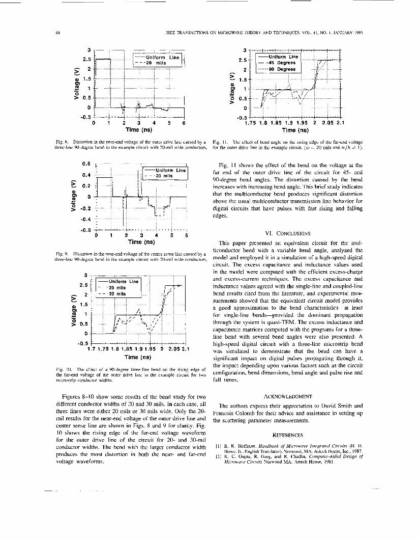
Fig. 8. Distortion in the near-end voltage of the outer drive line caused by a three-line %-degree bend in the example circuit with 20-mil wide conductors.
Fig. 1 I . The effect of bend angle on the rising edge of the far-end voltage for the outer drive line in the example circuit. (ut = 20 mils and w / k = 1).
Fig. 9. Distortion in the near-end voltage of the center sense line caused by a three-line 90-degree bend in the example circuit with 20-mil wide conductors.
VI. CONCLUSIONS
This paper presented an equivalent circuit for the mul- ticonductor bend with a variable bend angle, analyzed the model and employed it in a simulation of a high-speed digital circuit. The excess capacitance and inductance values used in the model were computed with the efficient excess-charge and excess-current techniques. The excess capacitance and inductance values agreed with the single-line and coupled-line bend results cited from the literature, and experimental mea- surements showed that the equivalent circuit model provides a good approximation to the bend characteristics-at least for single-line bends-provided the dominant propagation through the system is quasi-TEM. The excess inductance and capacitance matrices computed with the programs for a three- line bend with several bend angles were also presented. A high-speed digital circuit with a three-line microstrip bend was simulated to demonstrate that the bend can have a significant impact on digital pulses propagating through it, the impact depending upon various factors such as the circuit
Fig. IO. The effect of a 90-degree three-line bend on the rising edge of the far-end voltage of the outer drive line in the examule circuit for two configuration, bend dimensions, bend and pulse rise and ., microstrip conductor widths. fall times.
Figures 8-10 show some results of the bend study for two different conductor widths of 20 and 30 mils. In each case, all three lines were either 20 mils or 30 mils wide. Only the 20- mil results for the near-end voltage of the outer drive line and center sense line are shown in Figs. 8 and 9 for clarity. Fig. 10 shows the rising edge of the far-end voltage waveform for the outer drive line of the circuit for 20- and 30-mil conductor widths. The bend with the larger conductor width
voltage waveforms.
ACKNOWLEDGMENT
The authors express their appreciation to David Smith and ~~~~~~i~ Colomb for their advice and assistance in setting up the scattering measurements.
REFERENCES
I l l R. K. Hoffman, Handbook of Microwave Integrated Circuits (H. H. Howe, Jr., English Translator), Nonvood, MA: Artech House, Inc., 1987.
Microwave Circuits Norwood MA: Artech House, 1981. produces the most distortion in both the near- and far-end 121 K, C, Gupta, R, Garg, and R, Chadha, Compurer-Aided Design of

HARMS AND MITTRA: EQUIVALENT CIRCUITS FOR MICROSTRIP DISCONTINUITIES 69
P. Silvester and P. Benedek, “Equivalent capacitances of microstrip open circuits,’’ IEEE Trans. Microwave Theory Tech.. vol. MTT-20, pp. 511-516, Aug. 1972. P. Silvester and P. Benedek, “Microstrip discontinuity capacitances for right-angle bends, T junctions and crossings,” IEEE Trans. Microwave Theory Tech., vol. MTT-21, pp. 341-346, May 1973. A. Gopinath and B. Easter, “Moment method of calculating discontinuity inductance of microstrip right angled bends,” IEEE Trans. Microwave Theory Tech. (short paper), vol. MTT-22, pp. 880-883, Oct. 1974. P. Anders and F. Amdt, “Microstrip discontinuity capacitances and inductances for double steps, mitered bends with arbitrary angle, and asymmetric right-angle bends,’’ IEEE Trans. Microwal’e Theory Tech.,
A. Hill and V. K. Tripathi, “Analysis and modeling of coupled right angle microstrip bend discontinuities,” IEEE MTT-S Inf . Microwave Symp. I989 Dig., pp. I 143-1 146. P. Anders and F. Amdt, “Beliebig abgeknickte mikrostrip-leitungen mit bogenfoemigem uebergang,” Arch. Elec. Ueberrragung, vol. (band 33, heft 3) 33, pp. 93-99, 1979. B. Easter, ”The equivalent circuit of some microstrip discontinuities,” IEEE Trans. Microwave Theory Tech., vol. MTT-23, pp. 6.55-660, Aug. 1975. P. Silvester and P. Benedek, “Correction to ‘Microstrip discontinuity capacitances for right-angle bends, T junctions, and crossings,’ ” IEEE Trans. Microwave Theory Tech. (Letters), vol. MTT-23, p. 456, May 1975. A. Thomson and A. Gopinath, “Calculation of microstrip discontinuity inductances,’’ IEEE Trans. Microwave Theory Tech., vol. MTT-23, pp, 648455, Aug. 1975. M. Kirschning, R. H. Jansen and N. H. L. Koster, “Measurement and computer-aided modeling of microstrip discontinuities by an improved resonator method,” IEEE MTT-S Inr. Microwave Symposium 1983 Dip.,
P. Silvester and P. Benedek, “Equivalent capacitances for microstrip gaps and steps,’’ IEEE Trans. Microwave Theory Tech., vol. MTT-20, pp. 729-733, Nov. 1972. B. Neale and A. Gopinath, “Microstrip discontinuity inductances,” IEEE Trans. Microwave Theory Tech.. vol. MTT-26, pp. 827-83 I , Oct. 1978. A. Gopinath and C. Gupta, “Capacitance parameters of discontinuities in microstriplines,” IEEE Trans. Microwave Theory Tech., vol. MTT-26, pp. 831-835, Oct. 1978. A. Farrar and A. T. Adams, “Matrix methods for microstrip three- dimensional problems,” IEEE Trans. Microwave Theory Tech., vol.
A. Farrar and A. T. Adams, “Computation of lumped microstrip ca- pacities by matrix methods-rectangular sections and end effect,” IEEE Trans. Microwave Theory Tech. (Corresp.), vol. MTT-19, pp. 495497, May 1971. A. Farrar and A. T. Adams, “Correction to ‘Computation of lumped microstrip capacities by matrix methods-rectangular sections and end effect,’ ” IEEE Trans. Microwave Theory Tech. (Lett.), vol. M’IT-20, p. 294, Apr. 1972. M. Maeda, “An analysis of gap in microstrip transmission lines,” IEEE Trans. Microwave Theory Tech., vol. MTT-20, pp. 390-396, June 1972.
VOI. MTT-28, pp. 1213-1217, NOV. 1980.
pp. 495497.
MTT-20, pp. 497-504, Aug. 1972.
[20] P. D. Patel, “Calculation of capacitance coefficients for a system of irregular finite conductors on a dielectric sheet,” IEEE Trans. Microwave Theory Tech., vol. MTT-19, pp. 862-869, Nov. 1971.
(211 G. F. Engen and C. A. Hoer, “Thru-reflect-line: an improved technique for calibrating the dual six-port automatic network analyzer,” IEEE Trans. Microwave Theory Tech., vol. MTT-27, pp. 987-993, Dec. 1979.
[22] Circuit boards; Compliments of Rogers Corporation, Chandler, AZ. [23] Touchstone, EEsof, Inc., Westlake Village, CA. [24] T. S. Blazeck and R. Mittra, “Transient analysis of lossy multiconductor
transmission lines in nonlinear circuits,” IEEE Trans. Componenrs, Hybrids and Manufacturing Tech., vol. CHMT-14, no. 3, pp. 618427, Sept. 1991.
Paul H. Harms (S’83-M’92) received the B.E.E. degree in electrical engineering from the Georgia Institute of Technology in 1984 and the M.S. and Ph.D. degrees in electrical engineering from the University of Illinois in 1987 and 1992, respectively. He is currently a Postdoctoral Fellow in the De- partment of Electrical and Computer Engineering at the University of Illinois at Urbana-Champaign. His present interests are in the numerical and experimen- tal electromagnetic analysis of passive microwave components and electronic packaging for high-speed digital circuits.
Raj Mittra (S’S&M’57-SM’69-F’71) is the Di- rector of the Electromagnetic Communication Lab- oratory of the Electrical and Computer Engineering Department and Research Professor of the Coor- dinated Science Laboratory at the University of Illinois. He is a Past-President of AP-S. and he has served as the editor of the Transactions of the Antennas and Propagation Society. He won the Guggenheim Fellowship Award in 1965 and the IEEE Centennial Medal in 1984. He has been a Visiting Professor at Oxford University, Oxford,
England and at the Technical University of Denmark, Lyngby,. Denmark. Currently, he serves as the North American editor of the joumal AE\”U. He is President of RM Associates, which is a consulting organization providing services to several industrial and governmental organizations.
His professional interests include the areas of computational electromag- netics, electromagnetic modeling of electronic packaging, radar scattering, satellite antennas, microwave and millimeter wave integrated circuits, fre- quency selective surfaces, EMP and EMC analysis, and remote sensing.