equivalent circuits for discontinuities in balanced strip ... · equivalent circuits for...
TRANSCRIPT
EQUIVALENT CIRCUITS FOR DISCONTINUITIESIN BALANCED STRIP TRANSMISSION LINE
Arthur A. OlinerMicrowave Research Institute
Polytechnic Institute of Brooklyn
Abstract
Theoretical formulas are depived forthe equivalent circuit parameters of a va-riety of discontfnuties in balanced striptransmission line. These formulas aresimple fn form and are obtained by employ-%ng a small aperture procedure or a Babi-net equivalence procedure in conjunctionwith an approximate model of the line. Theresults for a number of discontlnuitieeare presented and comparison is made withthe available measured data.
I. Introduction
Approximate procedures are employedin this paper for the determination ofequivalent circuits for a variety of dis-continuity structures in balanced striptransmission line. Before discussingthese structures or the theoretical pro-cedures, it is desirable to mention cer-tain general qualitative considerations.Many of these general remarks are well-known to those working with strip lines.
1. Discontinuities in balanced striptransmission line will possess purely re-active equivalent networks if a) the dis-continuity is balanced, b) the outer platespacing Is less thanA/2, and, of course,c) the discontinuity structure containsno dissipative elements. If the dlscon-tlnulty structure is unbalanced (unsym-metrical with respect to the upper andlower portions of the line), the discon-tinuity will excite the dominant mode inradial transmission line (the lowest E-type (so-called pillbox) mode, similar tothe TEMmode in parallel plane line), andradiation will occur producing resistivecontributions to the equivalent circuit.
A little of this unbalance can betolerated and the radiation prevented byboxing In a small region surrounding thediscontinuity so that the unwanted ex-cited mode becomes the dominant mode inrectangular wavegutde, and by choostngthe dimensions such that the mode isbelow cut-off. Even a balanced discontin-uity will excite a variety of higherradial line modes, the lowest of thesebeing similar to the El (or TM1) mode inparallel plate line. None of these modeswfll propagate, however, if the platespacing is less than ~/2. Therefore,although the propagation of the dominantmode does not impose any condition on theplate spacing, a practical system musthave a plate separation less than 2i/2.
2. Most of the so-called transversediscontinuity structures (those whichoccupy a portion of the cross-sectionplane) in common use in coaxial line orrectangular guide do not have a counter-part in strip line because of construc-tional difficulties. As a result, it isdifficult in strip l%ne to obtain a shuntcapacitive discontinuity; a shunt induc.tance can be produced by use of a verticalwire or post. On the other hand, It iseasy in strip line to obtain eitherseries inductances or capacitances.
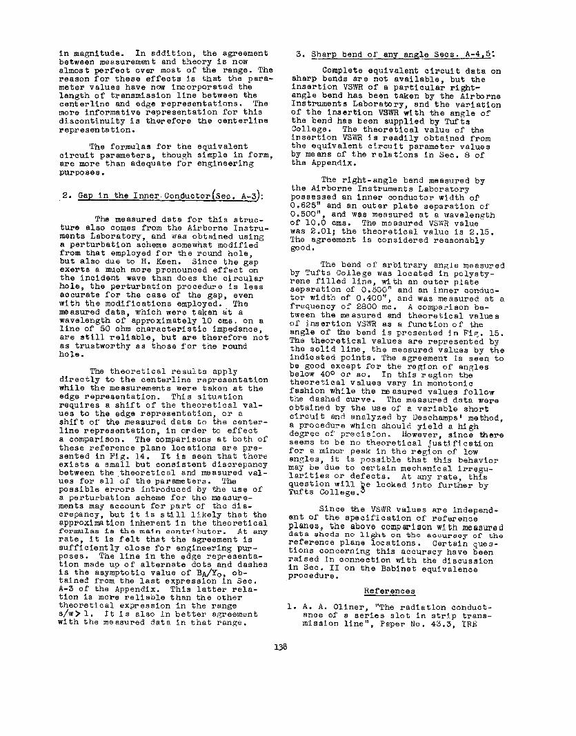
3. It is possible also to produce Ina simple fashion a series of resonantdiscontinuity. An example of how this maybe obtained is the followlng. A narrowgap extending completely across the fnnerconductor is known to be a series capactty(see Fig. l(a)). On the other hand, therectangular slot of Fig. l(b) (which maybe photo-etched without any difficulty) isa serious inductance. The proper choiceof length< of the slot will produceresonance. It is of interest to note thatthis length for resonance must of necessi-ty be consi.detiably less than A/2.
4. The dominant mode In balancedstrip line is a TEM mode so that the fielddistribution can be determined rigorouslyby conformal mapping procedures. Onecannot apply these methods to the highermodes, however, so that it is quite diffi:cult to obtain the field distributions ofeven the first few higher modes, althou,ghtheir cut-off wavelengths may be fai~lyreadily computed. For the rigorous solu-tlon of discontinuity problems one musthave available the approximate Green~sfunction for the region. Since the geome-try of strip line is not separable, as itis for most waveguide shapes, the rigorousdetermination of the Green~s function is amajor task in itself. For this reason itbecomes advisable to resort to approxima-tion schemes in the determination of theequivalent circuit parameters of discon-kfnuity structures in strip llne. All ofthe efforts described herein have beenalong these latter lines.
A qualitative description of thetheoretical procedures employed in obtain-ing the equivalent circuit parameters of anumber of discontinuity structures instrip line is given in Sec. 11. An approx-imate model Is first derived, and twotheoretical procedures, a small apertureprocedure and a Babinet equivalence pro-cedure, are explained. The Babinet
134
equivalence procedure is illustrated byapplication to a sharp right angle bend instrip llne.
The equivalent circuit parametersfor a number of. specific discontinuitystructures are presented in the Appendix.The conductance expression for the radiat-ing slot was derived in previous work bythe writer, but all others were obtainedby means of the approximation proceduresoutlined in Sec. 11.
In Sec. III, the theoretical resultsare compared with the available measureddata. In this ’connection, the writer Isindebted to Mr. W. E. Fromm, Dr. E. G.Fubini, and Mr. H. Keen of the AfrborneInstruments Laboratory for their data onthe round hole and the gap in the Innerconductor of strip line and for the VSWRof a right angle bend in strip line, andto Dr. A. D. Frost of Tufts College forhis data on the VSWR vs. angle of bend fora bend of arbitrary angle in strip line.The measurements at Tufts College were
taken wfth a variable short circuit andthe data analyzed by meana of Deschsmpslmethod, The measurements on the roundhole and the gap, taken at the AirborneInst:rumenta Laboratory, were made using anovel and Interesting perturbation schemedue to H. Keen.
The details of the derivations ofthe theoretical expressions are not givenhere but will be Included in a more com-prehensive report issued by the Polytech-nic Institute of Brooklyn under a contractwith the Air Force Cambridge ResearchCentar.
II. Theoretical Methods
1. ~le Approximate Model
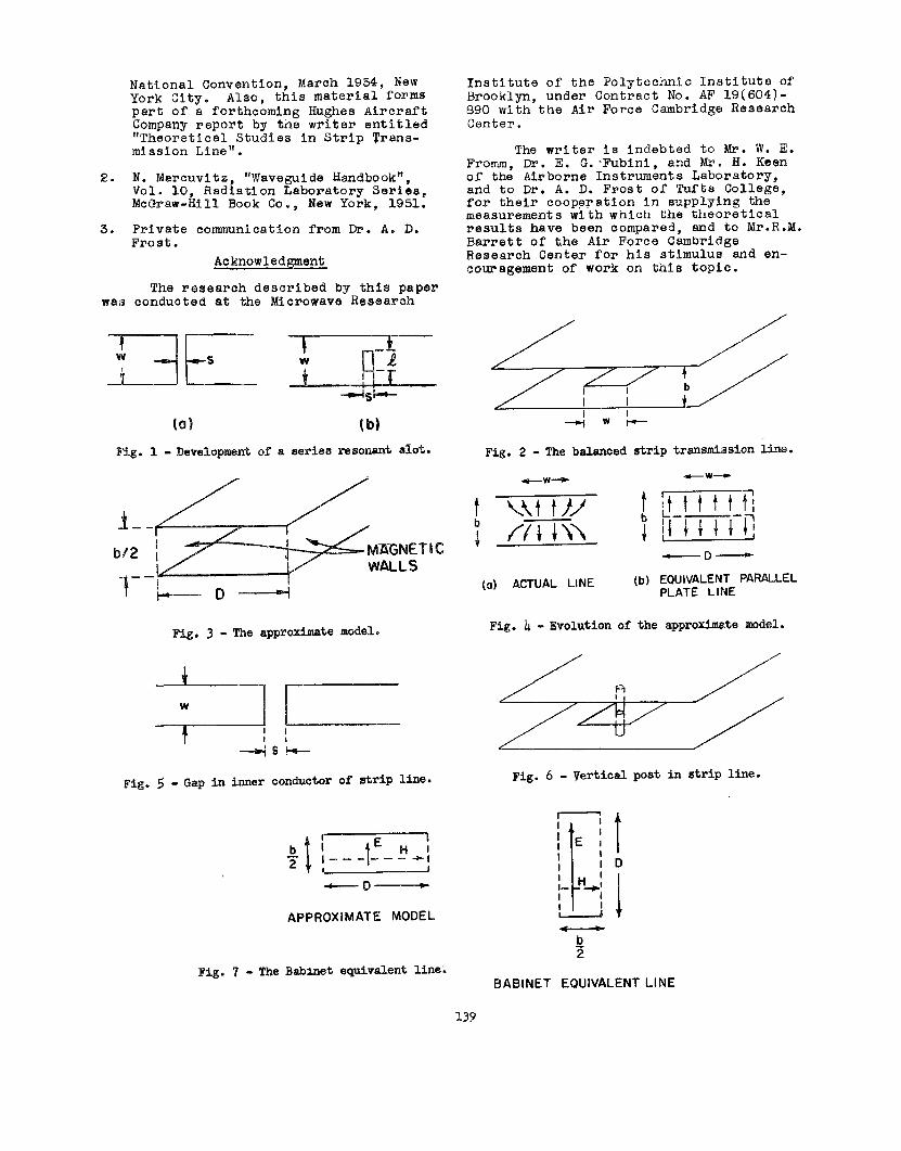
The balanced stir%p transmission lineconsidered @re, with an inner conductorof zero thickness, $s indicated In Fig. 2.Because of the formidable task, mentionedabove , of obtaining the appropriateGreenfs functfon for the geometry of Fig.2!, the approximate modelof Fig. 3 isemployed in the determination of theequivalent circuit parameters for discon-tfnuities in the llne. The width D of theline Is related to the actual center stripwidth. W by ‘
D= b K (k)/K (k!), (la)
wherek . tanh (Ww/2b),
and where K (k) is the complete ellipticintegral of the first kind of modulus k.When w/b70.5, corresponding roughly tocharacteristic impedances less than 100ohms, D is given to an excellent approxi-
mation by
D=w,~h2n (lb)
The line has electric walls (short cXr-cuits) for the top and bottom plates andmagnetic walls (open circuits)’ for theside walls. In effect, then, the approx-imate model is a portion, of width D, of aparallel plate transmission line ofinfinite width.
The evolution of thfs model from theactual geometry is ahown in Fig. 4. Thefringing of the electric field lines ~fthe dominant mode in the actual. geometry,shown in Fig. 4(a) , may be compensated forby extending the inner conductor width andplacing magnetic walls on the sides of theline . If the extended width has the valueD specified by (la), structures (a) and(b) of Fig. 4 have identtcal characteris-tic impedance values. Structure (lb)may beviewed as two identical poptions of paral-lel plate transmission line placed back toback, and any incident wave will divideequally into both portions. Since any,balanced discontinuity 5.n the line wI1lreflect the same proportion of the inci-dent wave in both top and bottom portions,and since this proportion is also that forthe total wave, it is not necessary whendealing with normalized quantities toretain both halves of the llne. Thus, inthe analysis of balanced discontinuitieswhich are described in terms of normalizedquantities one need consider only one-halfof the structure and may thus employ theapproximate model of Fig. 3.
The equivalent structure of Fig.4(b)has been applied by the writer to theevaluation of the normalized conductanceof a radiating slot cut in one of theouter conductors. (Since this discontin-uity structure is unbalanced, both halvesof Fig. d(b) were necessary). The resultobtained was compared with that derivedvia a rigorous conformal mapping procedureusing the original strip line geometry ofFig. 2, and the agreement was excellent.The results for the radiating slot areincluded herein as Sec. A-1 of the Appen-dfx. For many discontinuities, the use ofthe approximate model should yield verysatisi’actory approximate results.
As an almost dfrect consequence ofthe approximate inodel one can obtain theequivalent circuit parameters of a gap inthe Inner conductor of strip lfne (seeFig. 5). Since the gap extends completelyacross the width of the inner conductor,the dlscontinui.ty may be approximated by agap extending completely across the bottomface, say, of the approximate model, andtherefore by a gap of infinite width in aparallel plate waveguide of infkitewidth. The solution for the latte~ situa-
135
tion is obtainable from the already avail-able solution for the E plane slit coupl-ing Of rectangular guides, given on PP.
373-375 of the Javeguide Handbook2. (It
may be noted that parameter Bb of theequivalent circuit of Fig. ‘7.1-1, on P.374, should be a capacitance rather thanan inductance as given there.) ‘The
equivalent circuit parameters for the gapIn strip line are presented in Sec. A-3 ofthe Appendix, and the comparison oftheoretical results with measwed data iagiven in Sec. III. The theoreticalexpressions yield the centerline repre-sentation directly; the results for theedge representation are obtained by shift-ing the centerline representation resultsthrough the appropriate lengths of trans-mission line.
An asymptotic form, valid for S)jw,for the parameter BA/Yo of the edge repre-sentation is also given in Sec. A-3. Thi Sform i.s obtained from the results for theE-plane bifurcation presented on pp. 253-255 of the WaveguLde Handbook2.
2. Small Aperture Procedure
One very useful procedure forobtaining reasonably accurate approximatevalues for the circuit parameters of adiscontinuity structure employs well-knownIIgmall aperture” ‘r “stored power” con-siderations together with a variationalexpression. An aperture type variationalexpression, for series,type elements, forexample, may be written generallY as
B= Stored Power, (2)g Y. ~ltag~2
where a trial aperture electric field Emust be inserted into both numerator anddenominator. The voltage term is then ofthe form
JrVoltage = ~ x g . ~ds , (3)
aperture
where% is an appropriate mode functionwhich depends on the nature of the excita-tion of the discontinuity and on the typeof waveguide. The determination of thestored power is always the formidableportion of any such evaluation, sLnce itinvolves integrations over all the highermodes of the waveguide.
The use of the “small apertures” or“stored power” considerations avoids thenecessity for a separate evaluation of thenumerator of (2). Instead, one seeks thealready available solution for a similarproblem in a different waveguide croas-section. If the guide walls which ared~fferent in the two problems do notsubstantially influence the stored power(i.e., speaking loosely, the distortion
of the field lines) in the neighborhoodof the discontinuity, a property whichholds for “small apertures”, theseconsiderations state that the storedpowers for the two problems may be takento be equal. The stored power expressionis thus abatracte.d from this similarproblem by setting it up also in varia-tional form, even though it may not havebeen solved originally in this manner.The similar problem must,. of course,involve a discontinuity of the same shapeand with the same manner of excitationas in the original problem. The desiredsusceptance value is then equal to thealready known susceptance value multi-plied by the rahfo of the pertinentdenominators.
ThTs procedure has been employed in
obtaining the equivalent circuit para-meters given in Sec. A-2 of the Appendixfor the round hole in the inner conductorof strip line. The theoretical resultsapply directly to the centerline repre-sentation; the results for the edge repre-sentation are found by shifting thecenterline representation results throughthe appropriate lengths of transmissionline. Two different variational expres-sions are required; one for parameter
Ba/Yo, obtained by symmetrical electricfieldexcitation of the hole, end one forthe parameter combination (Ba/Yo +2Bb/ye),resulting from, anti-symmetric electricfield excitation. The similar problem,for which the SOIU ion is given in the
8tiaveguide Handbook on pp. 375, 376, iS
that of E-plane aperture coupling ofrectangular waveguides. The details ofthe derivations will not be presentedhere.
Other discontinuity structures forwh%ch the equivalent circuit parametersmay be found in this manner are the smallslot in the Inner.. conductor of strip line(shown in Fig. l(b)), and the verticalpost indicated In Fig. 6. This peat maybe of round, elliptical or rectangularcross-section, and may be perfectly con-ducting or made of dielectric material.Finally, the parameters for a hole ofelliptical, rather than round, shape mayalso be found by using the WaveguideHandbook” pages mentioned above in connec-tion with the round hole.
3. Babinet Equivalence Procedure
When the Babinet equivalent of theapproximate model of Fig. 3 is taken, onehas available almost immediately thesolutions for a variety of discontinuitiesin strip line. The Babinet equivalent ofa structure is found by replacing allmagnetic walls by electric walls and vice-versa, and by replacing lines of E bylines of H and lines of H by lines of -E.
1%
The equivalent circuit of the originaldiscontinuity structure la then the equiv-alent circuit dual to that describing theBabinet equivalent discontinuity struc-ture. The numerical values of the cor-responding duah elements are identical.
The line which is the Babinet equiv-alent of the approximate model of Fig. 3is ahown in Fig. 7, and is seen to beanother section of parallel plate linerotated through 90°. Its use in the solu-tion of discontinuity problems will beillustrated with reference to the sharpright angle bend in the inner conductor ofstrip line.
A top view of the inner conductor ofa right angle bend in strip line is ahownin F’ig. 8(a), while a top view of the samebencl in the approximate model is indicatedin Fig. 8(b). The bend in the Babinetequivalent line is illustrated by Fig.8(c),and is seen to be a right-angle E-planebenci (or E-plane corner) in parallel platetransmission line. One can find the
equivalent circuit for the E-plane cornerat the terminal planes T2 and T2 in theBabinet equivalent line by looking up pp.312, 313 of the Waveguide Handbook2. This
circuit la shown in Fig. 9(a). The equiva-lent cirouit appropriate to the approxi-mate modelof Fig. S(b) at the terminalplanes T1 and T2 is thus the dual of thatof Fig. 9(a), and is given in Fig. 9(b).The specific circuit parameters, which aregiven in Sec. A-4 of the Appendix, areobtained by making the appropriate dualsubstitutions in relations 3(b) and 4(b)on p. 313 of the Waveguide Handbook.
The equivalent circuit parametersfor the aharp bend of any angle, theeudd!en change in width and the Tee junc-
tion, giVf3n in the Appendix, have all beenobtained by the use of the Babinet equiva-lent line. Although not listed in the!.ppendix, the results for a circular bend,a junction between a straight length anda tapered length of line, and a 1200 Yjunction either have been or can also bedetermined by this procedure. The sharpbendl of any angle is included here sincemeasured data are avsilable which permitcomparison with the theoretical results.
The sudden change in width and theTee junction are presented here, eventhough no measurements are available,because of features of interest in theirequivalent circuits. For the change inwidth, one finds a series inductancecha~acterizing the discontinuity, in con-trast to the shunt inductance obtained fora change in width in rectangular wave -gufde and to the shunt capacitanceobteined for a change in height in rectan-gular guide or a change in inner or outerconductor radius in coaxial line. The
Tee Junction equivalent network possessesH plane symmetry, as would be expected,but its reference plane in the stub lineis not shifted by A/4 as is the case forthe corresponding form of the network inan H plane Tee in rectangular waveguide.
In some of these discontinuitiessome error may be present in the locationof the appropriate reference planes. Forexample, in the change in width, thereference plane T in Sec. A-6 of theAppendix is seen not to coincide with theplane of the actual change In width but islocated a distance (b/(~2 away from it.This distance is expected to be moreaccurate if a significant change in widthis present; if the change in width issmall, however, this distance is expectedto be less. Small errors of this type inthe location of the reference planes areinherent in the Babinet equivalence pro-cedure .
III. Comparison with Measured Data
With the exception of the radiatingslot, which was discussed eleewhere~pmeasured data are available for only threeof the strip line discontinuity structureslieted in the Appendix. These are theround hole, the gap, and the sharp bend.
l.Round Hole in the Inner Conductor{S~A-21:
The measured data on this discontin-uity structure comes from the AirborneInstruments Laboratory, and was obtaj.nedusing the perturbation scheme of H. Keen.The measurement were taken at a wave-length of approximately 10 ems., on linesof 50 and 75 ohms characteristic imped-ance. Both the measurements and thetheoretical results apply directly to thecenterline representation so that the com-parison is best made there. The comparisonis also a very sensitive one because theparameter values are so small, or so large,depending on the parameter (i.e., the rourdhole does not exert a very pronounced dis-turbance on the incident wave). such acomparison is indicated by the curves ofFigs. 10 and 12, for lines of 75 and 50ohms characteristic impedance, respective-ly . The theoretical valuea are indicatedby the solid lines , while the measureddata are represented by the indicatedpoints and the dashed lines connectingthem. It is seen that the agreement isreasonably good. One notes that all ofthe circuit elements are inductive in thisrepresentation.
Comparison between the measured andtheoretical values at the edge represents.tion Is afforded by Figs. 11 and 13. Itis seen that the shunt arms have nowbecor,e capacitive, and that these para-meter values have substantially increased
137
in magnitude. In addition, the agreement
between measurement and theory is nowalmost perfect over most of the range. Thereason for these effects is that the para-meter valuea have now incorporated thelength of transmission line between thecenterline and edge representations. The
more informative representation for thisdiscontinuity is therefore the centerlinerepresentation.
The formulas for the equivalentcircuit parameters, though simple in form,are more than adequate for engineeringpurposes.
(2. Gap in the Inner.Conductcw Sec. A-3 :
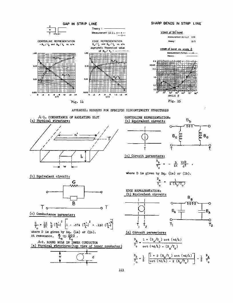
The measured data for this struc-ture also comes from the Airborne Instru-ments Laboratory, and was obtained using
a perturbation scheme somewhat modifiedfrom that employed for the round hole,but also due to H. Keen. Since the gapexerts a much more pronounced effect onthe incident wave than does the circularhole, the perturbation procedure is lessaccurate for the case of the gap, evenwith the modifications employed. Themeasured data, whfch were taken at awavelength of approximately 10 ems. on aline of 50 ohm characteristic impedance,are still reliable, but are therefore notas trustworthy as those for the roundhole.
The theoretical results applydirectly to the centerline representationwhile the measurements were taken at theedge representation. This situation
requires a shift of the theoretical val-ues to the edge representation, or ashift of the measured data to the center-line representation, in order to effecta comparison. The comparisons at both ofthese reference plane locations are pre-sented in Fig. 14. It is seen that thereexists a small but consistent discrepancybetween the ,theoretical and measured val-ues for all of the parameters. Thepossible errors introduced by the use of
a perturbation scheme for the measur-ements may account for part of the dis-crepancy, but it is still likely that theapproximation inherent In the theoreticalformulas %s the main contributor. At any
rate, it is felt that the agreement issufficiently close for engineering pur-poses. The line in the edge representa-tion made Up Of alternate dots and dashesis the asymptotic value of B~Yo, ob-tained from the last expression in Sec.A-3 of the Appendix. This latter rela-tion Is more reliable than the othertheoretical expression in the ranges/w>l. It Is also in better agreementwith the measured data In that range.
3. ~harp bend of any angle Sees. A-4,5Z
Complete equivalent circuit data onsharp bends are not available, but theinsertion VSWR of a particular right-angle bend has been taken by the AirkorneInstruments Laboratory, and the variationof the insertfon VSViR with the angle ofthe bend has been supplied by TuftsCollege. The theoretical value of theInsertion VSWR is readily obtained fromthe equivalent circuit parameter valuesby means of the relations in Sec. 8 ofthe Appendix.
The right-angle bend measured bythe Airborne Instruments Laboratorypossessed an inner conductor width of0.625” and an outer plate separation of0.500”, and was measured at a wavelengthof 10.0 CISS. The measured VSWR valuewas 2.01; the theoretical value is 2.15.The agreement is considered reasonablygood.
The bend of arbitrary angle measuredby Tufts College was located in polysty-
rene filled line, with an outer plateseparation of 0.50G1! and an inner conduc-tor width of 0.400”, and was measured at afrequency of 2800 mc. A comparison be-tween the measured and theoretical valuesof insertion VSWR as a function of theangle of the bend is presented in Fig. 15.The theoretical values are represented bythe solid line, the measured values by theindicated points. The agreement is seen tobe good except for the region of anglesbelow 400 or so. In this region thetheoretical values vary in monotonicfashion while the ~asured values followthe dashed curve. The measured data wereobtained by the use of a variable shortcircuit and analyzed by Deschampsl method,a procedure whtch should yield a highdegree of’ precis?on. However, since thereseems to be no theoretical justificationfor a minor peak in the region of lowangles, it Is possible that this behaviormay be due to certain mechanical irregu-larities OP defects. At any rate, thisquestion will be looked into further byTufts College.3
Since the VSWR values are independ-ent of the specification of reference
planes, the above comparison wtth measureddata sheds no light on the accuracy of the$eference plane locations. Certain ques-tions concerning this accuracy have beenraised in connection with the discussionin Sec. II on the Babinet equivalenceprocedure.
References
1. A. A. Oliner, “The radiation conduct-ance of a series slot in strip trans-mission line’!, Paper No. 43.3, IRE
138
National Convention, March 1954, NewYork city. Also, this material formspart of a forthcoming Hughes AircraftCompany report by the w~lter entitledt~Theoretical Studies in StriP ~rsns-
mission Line’!.
2. N. Marcuvitiz, “Waveguide Handbook”,Vol. 10, Radiation Laboratory Series,McGraw-Hill Book Co., New York, 1951.
3. Private communication from Dr. A. D.Frost.
Acknowledgment
The researah described by this paperwas conducted at the Microwave Researoh
:3E(01
Fig. 1 -Development of
4 .$Lw
t(-J1I l–
-d$ka--
[b)
a series resonant dot.
Institute of the Polytechnic Institute of$rooklyn, under Contract No. AF 19(604)-890 with the Air Force Cambridge ResearchCenter.
The writer is indebted to Mr. W. E.Fromm, Dr. E. G. ’Fubini, and Mr. H. Keenof’ the Airborne Instruments Laboratory,and to Dr. A. D. Frost of Tufts College,for their cooperation in supplying themeasurements with which the theoreticalresults have been compared, end to Mr.R.M.Barrett of the Air Force CambridgeResearch Center for hls stimulus and en-couragement of work on this topic.
AZ_&-iw+’-
Fi.g. 2 - The balanced strip tremamission line.
Fig. 3 - ‘Me approximate model.
-4jS”+
Fig. S - (lap in inner conductor of strip line.
~D~
APPROXIMATE MODEL
—D—*
(a) ACTUAL LINE (b) EQUIVALENT PARALLELPLATE LINE
Fig. h - Evolution of the approximate model.
Fig. 6 - Vertical post in strip line.
~1I
i
IE:I
I t1I IDI,- H+!I II I‘1
b%’
Fig. ? - The Babinet equivalent. line.BABINET EQUIVALENT LINE
139
IFw
w
(.) PHYSICALLINE
,+= f+
(b) APPROXIMATE (c) WBINET
MOWL EWIVALENT LINE
M.g. 8 - Right angle bend.
ROUND HOLE IN STRIP LINE75 ohm ii ne
CENTERLINE . REPRESENTATION
(.) E PLANE CORNER (b) STRIP LINE BEND
Fig. 9 -maal equivalent circuit s.
ROUND HOLE IN STRIP LINE
75 ohm I ine
EDGf REPRESENTATION
Theory :.
Meoeurement (A.I.L.):- -*-
?w 0+ Theory :
Measurement (A.I.L.): o
B. I Y,. vs. d/w Bb fYo vs. dlw
Fig. 10
ROUND HOLE IN STRIP LINE50 ohm line
CENTERLINE REPRESENTATION
8, / Y9 vS.dlw
-.001
e,~
-.01
-02
Theory :Measurement ( A.I L.X--f+-
Tw
O:.ld
-T
8$ 1% VS. dlw
eA I Y. VS.dm
0 la
%~
0 t6
0,14
012
010
0.2 0.4 0.6 08dlw
%B / Ye VS.dlw
ROUND HOLE IN STRIP LINE
50 ohm line
EDGE REPRESENTATION
Theory :
Meosurenent ( A. I.L.): o -
e B / Yo ‘s. dlw
d/w
Fig. 12
140
Fig . 13
GAP IN STRIP LINE SHARP BENDS IN STRIP LINE
Theory:VSWR of 90” bendMeasurement’ (AI L ):--X --
-- 0--measurement (A. I.L.]: 2.o1
CENTERLINE REPRESENTATION EDGE REPRESENTATION thmr y, 21 s
- e. / Y. .md Ob/ Y. vs. SIW eA/ Y. md BB/ Y. vs. s/w
Asymptotic t hecret icol volue,.+ n. 1 v . —. —.—. —
VSWR of bend vS. anale ememurement iTufts )---o--
theory —-
.—.0 .9. a .6 .0 ID 1.2 L4
dwo .2 .4 .6 .S 1.0 1.2 la
s/w ANGLE 8
15Fig.
FOR SPECIFIC DISCONTINUITY STRUCTURES
‘Fig. 14
APPENDIX : RESULTS
CENTERLINEREPRESENTATION:(b) Equivalent circuit:
~T”
A-I. CONDUCTANCE OF RADIATING SLOTQI) Physical structure I
//
Bb
// /
I
o-+_T/ / / /
I I LI I
(c) Circuit parameters:
‘b .~-’-#W k--
(la) or (lb),where D is given by Eq.@) Equivalent circuit:
AEDGEREPRESENTATION:(b) Equivalent circuit:
o t o
BB
o1[
IbIII
~) Conductance p~~eter *
5
[—’g }(.+2 1-Y. 1
.374 (+)2 + .130 (+; 1[ T2
where D is given by Eq. (la) or (lb).At resonance, ~ ~ &!? .
oh
(c) Circuit parameters:
‘A 1 + (Ba/Yo ) oot (~d/k)-.A-2. ROUND HOLE IN iNNER CONDUCTOR
l(a) Physical structure: top view of inner conductor.Y*
cot (~d/k) - (Ba/Yo)
BB 1
[ 1
1 + 2 (Bb/Y ) 00t (nd~) ~
q“?— --
cot (rid/k) - 2 (Bb/yo) 2
lb
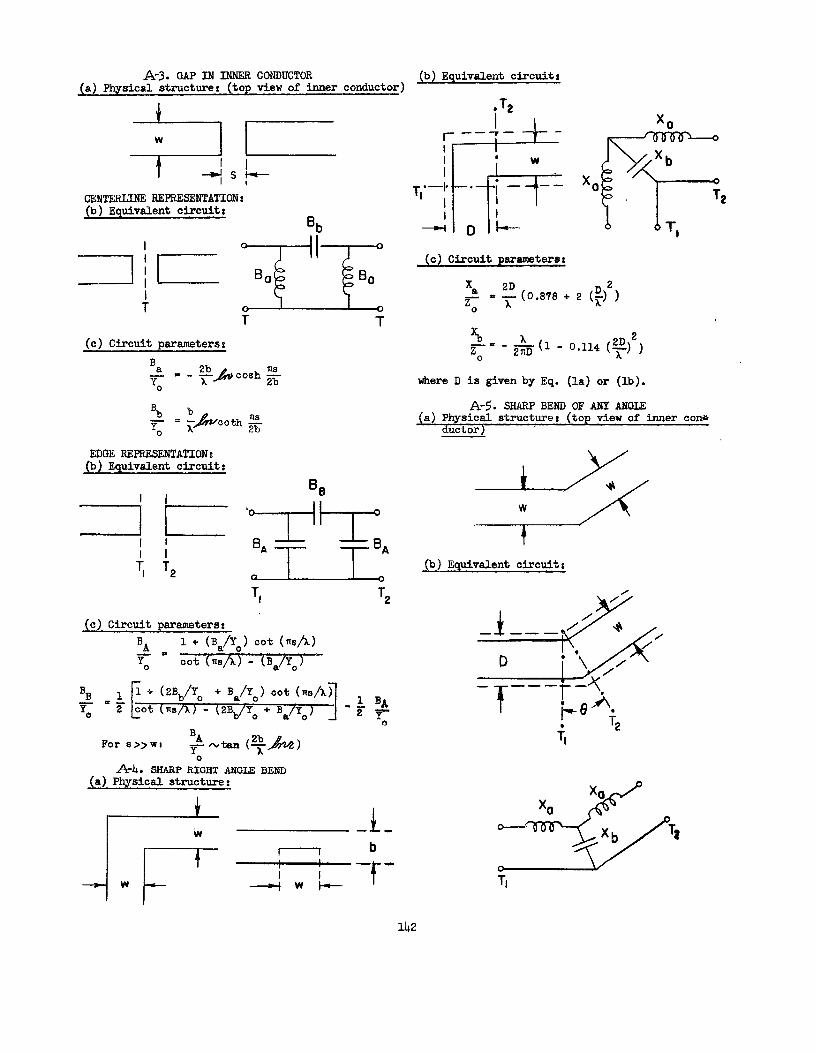
A-3. GAP IN INNBR CONDUCTOR (b) Equivalent circuit:(a) Physicsl structure: (top view of inner conductor)
+
w
+u-1
CENTERLINE REPRESENTATION:(b) Equivalent circuit:
‘b
3iI
‘[~~ B. ‘ Ba
+T T
(c) Circuit parameterss
B
<.- ~~.osh g
EDGE REPRESENTATION $(b) Equivalent circuit:
T1 T2
(c) Circuit parameters:
‘A1 + (B@) cot (nS~)
~= cot (ma ) - (Ba/Yo )
‘B
[
~ 1 + (2 Bb/Yo J+Ba/Yo) cot ( m/A)
q-~BA
= ~ Cot (llS/~j - (2 Bb/Yo + Ba/y 2~a
For s>>w: ‘Ay **E (~~)”
oA-LJ. SHARPRIGHT ANGLEBEND
(a) Physicsl structure:
FL+I
Iv. w
I
T,”—; “ j — ‘-
I
--ho-
X.
FOx~
X.T2
T,
(c) Circuit parameters:
Xa
< = : (0.878 + 2 (;)2)
%—.z - *(1 -0.114 (+)2)
o
where D is given by Eq. (la) or (lb).
A+. SHARP BEND OF ANY ANGLE(a) Physical structure: (top view of inner con*
duct or j
Ux
w
t
(b) Equivalent circuit:
I
1!42
(c) Circuit parameters%
xb=. ~oo,:~ 2nD
~qj+w-bf+ljwhere ~ (x) is the logarithmic derivative of xl,and where D is given by Eq. (la) or (lb).
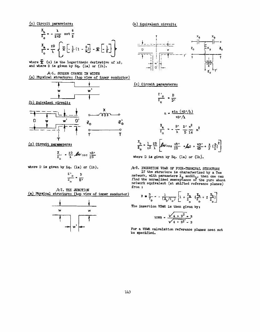
A-6. SUDDENCHANGEIN WIDTH&Physicel structure: (top view of inner conductor)
! 1 t
w w’
, 4
~Eaivalent circuit:!
x
T
x . ?24%.s. ~q
where D is givenby Eq. (la) or (lb).
Zlo ~
~-ijr
A-7. m JUNCTION
T
(b) Equivalent circuit:
.J--__~-. -J._
Ir
-;--.., ~ w,!:-
—-. —.—T’
w’ 1
-j D’ ~
(c) Circuit parameters:
Z!. D
~ ‘~
--tJ-T T
nn
Z; T’
where D is givenby Eq. (la) or (lb~.
A-8. INSERTIONVSWROFFCWIZ.mNALSfRIucT~If the structure is chexacterized by a Tee
network, with parameters X sndxx , then one canf! ? the pure shuntfind the normalized suscep ante o
network equivalent. (at shifted reference planes)from t
@_Physical structure: (top view of inner conductor) Bs+=- 1[
~ x~
I I o 1nj7gT~4zo ~~+z~)t t
L
The insertion VSWHis then given
+-l+
~m=A7+B
m- B
-lw- For a Wh!R calculation referencebe specifked.
by:
planes neefl not
11!3