entc4277 instrumentation and process control lab report course projects/entc 4277 instrumentation...
TRANSCRIPT

X i q i a o W a n g L a b R e p o r t | 1
ENTC4277 Instrumentation and Process Control
Lab Report
Xiqiao Wang
E00340095
College of Business & Technology
East Tennessee State University
April 30, 2011

X i q i a o W a n g L a b R e p o r t | 2
Contents
Lab 1 Thermocouple-----------------------------------------------------------------------------------3
Lab 1 Appendix-----------------------------------------------------------------------------------------21
Lab 2 Strain Gauge------------------------------------------------------------------------------------37
Lab 2 Appendix-----------------------------------------------------------------------------------------57
Lab 3 Stepper Motor----------------------------------------------------------------------------------69
Lab 3 Appendix-----------------------------------------------------------------------------------------97
Lab 4 Vibration-----------------------------------------------------------------------------------------115
Lab 4 Appendix-----------------------------------------------------------------------------------------131
Safety Note: Ware safety goggles whenever soldering, and wash hands after soldering.

X i q i a o W a n g L a b R e p o r t | 3
ENTC4277 Lab Report 1 Thermocouple
Part1. Generate and Observe Lissajous Curves
Brief Description
Definition
A Lissajous figure is produced by taking two sine waves and displaying them at right angles to
each other. It is actually describes the harmonic motions of one point along both X-axis and Y-
axis. In our electronic lab, we can demonstrate Lissajous curves by using two function
generators and a dual trace oscilloscope.
Characteristics
The appearance of the figure is highly sensitive to the frequency ratio of the two input sine
waveforms, even though the phase shift will also affect the shape of Lissajous figure. For a
frequency ratio of 1, the figure is an ellipse, with special cases including circles(assuming the
amplitudes of each waveform is equal) when the phase shift is 90 degrees and lines when two
sine waveforms are in phase or out of phase. Other ratios produce more complicated curves,
which are closed only if the frequency ratio is rational. Otherwise the figure will not be stable
and close.
Practical use
1. The practical application of Lissajour curves is to determine the frequency ratio of two
sine waves in the old days and determine some simple phase shifts according to
corresponding patterns. If the Lissajous figure is stable and closed, then the frequency
ratio equals to the ratio of the greatest number of intersection points of the Lissajous
figure with a horizontal line and a vertical line.
2. Another important application of Lissajous figure is its ellipse’s figures. In a Linear Time
Invariant system, when the input is sinusoidal, the output will be sinusoidal with the
same frequency, but it may have different amplitude and some phase shift. Using an
oscilloscope that can plot one signal against the other (XY mode) to plot the output of

X i q i a o W a n g L a b R e p o r t | 4
the LTI system against the input to the LTI system produces and ellipse that is a
Lissajous figure for the special case of the same frequency. The eccentricity of the
resulting ellipse is a function of the phase shift between the input and the output, with
an eccentricity of 1 corresponding to the phase shift of ±90° and an eccentricity of +∞
corresponding to the phase shift of 0° or 180°.
Experimental procedures
1. Connect the “Trig Out” of the second function generator to the [Ext Trig/ Gate/ FSK/
Burst] connector of the first function generator. Connect the two function
generators to the oscilloscope.
2. Trigger Setup: Set the trigger source of the first function generator as “External”,
which means trigger signal come in via the rear-penal [Ext Trig/ Gate/ FSK/ Burst]
connector, and set the second function generator “Immediate”, which means
triggers are automatically generated so that the triggered sweep burst will operate
continuously.
3. Set the second function generator’s “Trig Out” on at rising or falling, which enable a
rising or falling edge out put trigger.
4. Set the “Sync” of the second function generator on, which allow me to enable the
front penal “Sync” output.

X i q i a o W a n g L a b R e p o r t | 5
5. Set the “Sync Setup” of the first function generator as “Carrier” and the second as
“Maker”.
6. Set the two function generator at the same amplitude, phase and frequency as initial
value, and then observe the wave form in the screen of the oscilloscope at the X-Y
display format. The Channel 1 input corresponding to the waveform along the X-axis
and Channel 2 the Y-axis.
Problem encountered
7. the two function generator won’t synchronize with each other and the phase shift
keep drifting slowly. After repeatedly adjustment of the trigger setting, I found it
doesn’t work. So I adjust the first function generator’s phase to +55° to make the
two sine waves in phase.
8. Adjust the frequency ratio of the two signals to different simple integral ratio led to
the Lissajous figures below. The phase shift did not stay zero due to the phase shift
drifting during the period of this experiment.
Phase shift is 0°, frequency ratio equals 1.

X i q i a o W a n g L a b R e p o r t | 6
Frequency ratio of Channel 1 against Channel 2 is 2.
Frequency ratio of Channel 1 against Channel 2 is 3.

X i q i a o W a n g L a b R e p o r t | 7
Frequency ratio of Channel 1 against Channel 2 is 4.
9. Using Multisim to generate Lissajous’ figure.
a. Draw simple circuit to generate two waveforms that have a phase shift of
90 degrees.
b. Observe the Lissajous figure using Osciliscope.

X i q i a o W a n g L a b R e p o r t | 8

X i q i a o W a n g L a b R e p o r t | 9
Part2. Thermocouple
Objectives
1. Detect temperature using a thermocouple connected to the SensorDAQ interface.
2. Learn the basics of LabVIEW programming while creating a visual thermometer.
Materials
1. Windows computer
2. LabVIEW
3. Vernier SensorDAQ
4. Thermocouple wire
5. AD595AQ monolithic thermocouple amplifier with cold junction compenstation
6. Vernier ThermoSensor.
Knowledge preparation
1. Thermocouple
a. Definition: thermocouple is a closed loop circuit combined with two different kinds
of metals. When the temperature on the two junctions is different, there will
generate a voltage related to the temperature difference in the circuit.
b. Calculations: the voltage generated by thermocouple is m mainly composed of
contact potential and thermo electromotive force. Practice indicated that contact
potential is the main part of thermocouple voltage.
The contact potential is the result of the different free electron density of
two metals and their diffusion; the temperature free electron density of the
two metals in that temperature affects the value of contact potential.
EAB(T)= (kT/e)ln(NAT/NBT), k is Boltzmann’s constant, e is electronic quantity
of an electron. If the material is not harmonious, then integration should be
used for the overall contact potential in the loop, otherwise, it is EAB(T)-
EAB(T0).
The thermo electromotive force is generated along the portions of the length
of the two dissimilar metals that is subjected to a temperature gradient.
Because both lengths of dissimilar metals experience the same temperature
gradient, the end result is a measurement of the temperature at the
thermocouple junction. The principle is that temperature stands for the

X i q i a o W a n g L a b R e p o r t | 10
average kinetic energy of particles in substances, there are more electrons
move from the hot end to the cold end than the reverse.
c. Laws of thermocouple:
Law of homogeneous material: A thermoelectric current cannot be sustained
in a circuit of a single homogeneous material by the application of heat alone,
regardless of how it might vary in cross section. It can be used to detect the
different metals.
Law of intermediate materials: The algebraic sum of the thermoelectric
electromotive forces in a circuit composed of any number of dissimilar
materials is zero if all of the junctions are at a uniform temperature. So if a
third metal is inserted in either wire and if the two new junctions are at the
same temperature, there will be no net voltage generated by the new metal.
Thus the hot end of thermocouple can be soldered on the surface of other
metal or be merged into molten iron separately.
Law of successive or intermediate temperatures: If two dissimilar
homogeneous materials produce thermal emf1 when the junctions are at T1
and T2 and produce thermal emf2 when the junctions are at T2 and T3 , the
emf generated when the junctions are at T1 and T3 will be emf1 +
emf2,provided T1<T2<T3.
Standard electrode law: Under the specific temperatures of hot end and cold
end, the overall voltage in the thermocouple composed of metal AB is the
sum of that in the thermocouple composed of metal AC and CB.
d. Applications of cold junction compensation:
When the cold end’s temperature is not zero, we can measure the cold
junction temperature and find the corresponding voltage in look up table and
add it with the voltage generated by the thermocouple, and then go back to
the lookup table again to find the real temperature of the measured object.
When the cold end’s temperature is not stable, we can use corresponding
unbalanced bridge or keep the cold end in a homothermal container with big
thermal inertia.
The compensation lead is used to extend the cold end of expensive
thermocouple away from hot environment to a place with stable and cold
temperature. So the material used should have the same thermoelectricity
characteristics within the range of 0°-100° and be less expensive. This is an
application of the law of successive or intermediate temperatures.
e. Advantages of thermocouple: good Low cost, rugged, very wide range.
f. Disadvantages of thermocouple: low sensitivity, reference needed.

X i q i a o W a n g L a b R e p o r t | 11
g. The reason for the thermocouple’s grounding: Although instrumentation amplifiers
have differential inputs, there must be a return path for their bias currents to flow to
common (ground). If this return path is not provided, the bases (or gates) of the
input devices are left floating (unconnected), and the in-amp’s output will rapidly
drift either to common or to the supply. Therefore, when amplifying floating input
sources such as transformers (those without a center tap ground connection),
ungrounded thermocouples, or any ac-coupled input sources, there must still be a
dc path from each input to ground. A high value resistor of 1 M to 10 M
connected between each input and ground will normally be all that is needed to
correct this condition.
Procedures
1. Make the thermocouple
a. Strip the protecting jacket at both ends of the thermocouple wire. Trist one end and
make sure there is no second conjunction before the bared metal wires go into their
insulating sleeves. Leave the other end separated and long enough to build the
circuit.
b. Solder the twisted end with soldering tin. Be sure to wear the safety goggle and
wash hands after soldering. Make the soldering as small as possible to minimize the
negative effect of thermal inertia on the dynamic response of thermocouple.
c. Find technical parameters about K type thermometer
Type K (chromel90 percent nickel and 10 percent chromium–
alumel)(Alumel consisting of 95% nickel, 2% manganese, 2% aluminium and 1%
silicon) is the most common general purpose thermocouple with a sensitivity
of approximately 41 µV/°C, chromel positive relative to alumel. It is
inexpensive, and a wide variety of probes are available in its −200 °C to
+1350 °C / -328 °F to +2462 °F range. Type K was specified at a time when
metallurgy was less advanced than it is today, and consequently
characteristics vary considerably between samples. One of the constituent
metals, nickel, is magnetic; a characteristic of thermocouples made with
magnetic material is that they undergo a step change in output when the
magnetic material reaches its Curie point (around 354 °C for type K
thermocouples).

X i q i a o W a n g L a b R e p o r t | 12
2. Build up circuit using AD595, thermocouple and SensorDAQ.
a. From the specifications of AD595, the specified performance of power requirement
is from 0V to 5V. So I choose it as the single supply. The output voltage range for
AD595A single supply is 0V~+Vs-2, besides it has a low impedance voltage output
of 10mV/C°, so the temperature range for this circuit will be 0C°~300C°.
b. Build the circuit as below.
Note: If the thermocouple is not remotely grounded, then the dotted line
connections in Figures 1 and 2 are recommended. So I connect Pin 1 to the
common ground. The yellow lead connects to Pin1 and the red one Pin14.

X i q i a o W a n g L a b R e p o r t | 13
c. Connect the USB port to the computer. Connect the screw terminal 5 to the
common ground and terminal 11, which is the analog input channel 0, to Pin9 for
single-ended measurement.
d. Because AD595 has a low impedance voltage output, and according to the Vernier
SensorDAQ specification, the analog input has a input impedance greater than 1 MΩ,
so it is not necessary to add a voltage follower between AD595 and SensorDAQ.
Note that the input resolution for the single-ended is 13 bits, and the system noise
for the single-ended is smaller than 5 mVrms. The absolute accuracy for +5V channel
is 3.15mV, for +/-10V channel is 10.5mV. The input impedance of AD595 is high,
which will be good to restrain the current in the thermocouple; and the input bias
current is 0.1µA, it may generate some error on the resistance of thermocouple.
These may have already be included in the K type thermocouple’s limited error,
2.2°C or 2%, whichever is greater. Besides, the AD595 A version has a calibration
accuracy of ±3°C.
e. Connect the Vernier ThermoSensor to Channel 2.
3. Write a LabVIEW program to demonstrate the temperature detected from the
thermocouple and realize other display functions.

X i q i a o W a n g L a b R e p o r t | 14

X i q i a o W a n g L a b R e p o r t | 15
a. Set up the Express VI by selecting Function Palette-Vernier SensorDAQ-analog
express.

X i q i a o W a n g L a b R e p o r t | 16
Select Add Channel and activate the ai0 analog input channels on the screw
terminal at the range of ±10V. This will be more safe for the interface circuit,
but will introduce a worse absolute accuracy. Then active channel 2 with the
calibration coefficients of Vernier Thermocouple.
Select Set Timing button to configure the Express VI sampling rate at 10
samples/sec, since it is less than 200samples/sec, the Express VI will return a
single data point every time the Express VI is called (this is corresponding to
setting the “Wait Until Next ms Multiple” at 1ms). The channel’s output
terminal is wired to either a Chart or a Numerical Indicator. Also select the
“Repeat” and “Average” button. Set the “Length of Experiment” at 10s.
Choose “Automatic” to make sure SensorDAQ uses Vernier Sensor Auto-ID
calibrations.

X i q i a o W a n g L a b R e p o r t | 17
b. Divide the AI0 by 0.01 to get the detected temperature, and connect the result to a
Thermometer and a Numeric Indicator. Then bundle the detected temperature with
the Vernier Thermocouple output to a Waveform Chart.
c. Use two Numeric Controls in the Front Panel to set the upper limit and lower limit.
d. In the Block Diagram Panel, use Case Structure to decide the condition of the
temperature.
Case 1: “Over Hot”, warning light on.
Case 0: “Work Well”, warning light off.
Case 2: “Too Cold”, warning on.
Case 3(default): when the input upper limit is less than or equal to the lower
limit, there will have a popup saying “setting error”, warning on, stop the
While Loop.
e. Set the Wait Until Next ms Multiple at 1ms.
f. Practice to use array, Intensity Chart and 3D Surface to demonstrate the collected
data.
4. Collect data.
a. Detect body temperature with fixed Y-scale and AutoScale Y.

X i q i a o W a n g L a b R e p o r t | 18
The error between two thermocouples circuits is about 1.1°C. The fixed Y-scale and
the Average selection in Setting Time (the first figure) make the waveform looks
stable. But the waveform without fixed (the second figure) can show details of the
Average graph of the waveform.
b. Detect cold water temperature.
The left figure shows the temperature using Average function, the right figure
without. Both are using AutoScale Y, so the difference is highlighted. The error
between two thermocouples circuits is about 1.9°C.
c. In room temperature, make the hot side of each thermocouple contact with each
other, we will observe the waveform as follows.

X i q i a o W a n g L a b R e p o r t | 19
Since the Vernier Thermocouple use K type thermocouple wire, we get to know that
this contact must be between the Nickel-Chromium and Nickel-Aluminum. The
difference between the two demonstrated temperature reflect a junction voltage
generated K type thermocouple in the temperature of 17°C (290K) (here we assume
the Vernier Thermocouple is accurate). By using the transfer characteristics of K type
thermocouple in 25°C, 44µV/°C, and by eliminating the measurement error of the
experimental circuit which is about 2.5°C, we get the
EAB(T=290K)=18.75°C*44µV/°C=0.825mV.
5. Source of error
a. K type thermocouple: limit of error, 2.2°C or 2%, whichever is greater.
b. The resistance in thermocouple circuit and the input bias current of AD595
(0.1µA)will generate a voltage drop on the thermocouple wire.
c. AD595A: The combined effects of cold junction compensation error, amplifier offset
drift and gain error determine the stability of the AD594/AD595 output over the
rated ambient temperature range.
Calibration error at 25°C: ±3°C.
Gain error at 25°C: ±1.5%
Stability vs. Temperature at 25°C: ±0.05°C/°C
Since a K type thermocouple deviates from this straight line approximation,
the AD595 will normally read 2.7 mV (that is 11µV*247.3 ) when the
measuring junction is at 0°C. This offset arises because the AD595 is trimmed
for a 250 mV output while applying a 25°C thermocouple input.
d. SensorDAQ:
Absolute Accuracy for single-ended screw terminal: ±10mV
(absolute accuracy includes offset and gain errors, nonlinearity, and noise).
6. Test the circuit.
a. From the manual of Vernier Thermocouple, we get to know that for most
circumstances, we do not need to calibrate this sensor. Because the manufacturer
has performed a very accurate factory calibration that is specific to each individual
sensor. This unique calibration is stored on the sensor, and will be loaded by any of
our data-collection programs that support auto-ID.

X i q i a o W a n g L a b R e p o r t | 20
b. We can calibrate the experimental circuit by resetting the Express VI.
Zero Channel: When this popup is active, you can apply a zero offset to the
sensor reading. Place a check mark next to the sensor. When you press the
Apply button the offset is created, so make sure that you have the sensor
aligned properly when you press the button. Note that this zero offset is not
stored once LabVIEW is closed. You will have to re-open the Express VI and
re-zero.
Adjust Calibration Coefficients: When Manual is selected, the calibration
coefficients and units become enabled. This allows you to modify the
coefficients. This would be useful if the sensor units are not accurate enough.
Most sensors have a linear conversion, so you could perform a two point
calibration test, determine more accurate coefficients, and apply them here.
Note that K1 is the slope value and K0 is the intercept. In addition, set the
slope = 1 and the intercept = 0 and units = Volts to send data as the sensor’s
raw voltage.

X i q i a o W a n g L a b R e p o r t | 21

X i q i a o W a n g L a b R e p o r t | 22

X i q i a o W a n g L a b R e p o r t | 23

X i q i a o W a n g L a b R e p o r t | 24

X i q i a o W a n g L a b R e p o r t | 25

X i q i a o W a n g L a b R e p o r t | 26

X i q i a o W a n g L a b R e p o r t | 27

X i q i a o W a n g L a b R e p o r t | 28

X i q i a o W a n g L a b R e p o r t | 29

X i q i a o W a n g L a b R e p o r t | 30

X i q i a o W a n g L a b R e p o r t | 31

X i q i a o W a n g L a b R e p o r t | 32

X i q i a o W a n g L a b R e p o r t | 33

X i q i a o W a n g L a b R e p o r t | 34

X i q i a o W a n g L a b R e p o r t | 35

X i q i a o W a n g L a b R e p o r t | 36

X i q i a o W a n g L a b R e p o r t | 37
ENTC4277 Lab Report 3 Strain Gauge
Abstract
In Lab2 of Instrumentation and Process Control, our main aim is to use instrumentation
amplifier to build a strain gauge measurement system. Through this task, we will learn the
characteristics of instrumentation amplifier and its typical applications. The first part of this
experiment is to verify the CMR vs. Frequency Characteristic Curve of AD621. The second part is
to use strain gauge and two stages of amplifier circuits and SensorDAC interface to build a
weight measurement system.
Keywords: strain gauge, CMR, AD621
Part1. Testing the common mode rejection ratio of AD621
Method

X i q i a o W a n g L a b R e p o r t | 38
Firstly, we connect the two inputs of the instrumentation amplifier together and to the output
of a signal generator, and set the signal generator output to a peak-to-peak amplitude usually
equal to the full common-mode range, from the datasheet of AD621, the input common mode
voltage range is ±Vs, but in consideration of the maximum output ability of the function
generator, we use 20Vp-p as the testing signal amplitude for the common mode rejection ratio.
Use the AC voltage channel of the digital multimater to test the common mode voltage output.
Since the displayed value of the AC voltage channel is RMS value, from the measured value of
amplifier output and the calculated RMS value from the Vp-p output of the function generator,
we can then calculate the common-mode gain.
The measurement frequency normally depends on the application for which the IA is intended.
Here our aim is to verify the CMR vs. frequency figure shown in the AD621 datasheet, and from
this figure, the manufacturer only gives the CMR curve corresponding from DC to 100kHz. So
this is my arrangement of the measurement frequency. Within this frequency range, the
differential gain can be considered as a constant, we only need to minus the differential gain in
dB by the common mode gain in dB. For higher frequency range, the differential gain drops
dramatically, AD621 is no longer suitable for the specific application.
Figure.1 CMRR test setup for instrumentation amplifier.
At dc level, CMRR is measured by applying an input voltage step. After the resulting transient is
fully settled, you can measure the magnitude of the output voltage step.
Results

X i q i a o W a n g L a b R e p o r t | 39
The CMR vs. Frequency figure given by the AD621 datasheet is shown below. It is measured
under the condition of zero to 1KΩ source imbalance, which means the impedance of the
connection or the path between the reference pin of AD621 to the real ground. In addition, the
mismatching of the common mode voltage source, which means the existence of differential
element of the common mode input voltage, can also affect the precision of our CMRR
measurement.
The CMR data from my experiment shows an overall declining trend of it against frequency, and
the CMR value at DC level and 1KHz and 10KHz match the reference values well. For other

X i q i a o W a n g L a b R e p o r t | 40
values, the common mode rejection ratio is lower than the datasheet values between DC and
1KHz, and higher than datasheet values above 10KHz.
Discussion
The evaluation methods for an op-amp and an in-amp are different.
Common mode signals can be steady-state DC voltages (such as the 2.5 V from the strain gauge
bridge we used to build the Assignment 2) or they can be AC signals such as external
interference. In industrial applications, the most common cause of external interference is
picked up from 50/60 Hz mains sources. However, we also need to be conscious of interference
caused by harmonics the mains frequency. In industrial environments, harmonics of the mains
frequency can be significant up to the seventh harmonic (350/420 Hz) (Nash, 1998). According
to the datasheet of AD621, the differential gain remains stable until the input differential
frequency reaches about 100kHz, but we see that when the differential gain is set to 10, the
CMRR remains relatively flat out to about 100Hz, while the CMRR begins to decrease at 10Hz
with a differential gain of 100. This means that the CMRR drop to about 100dB at the
differential gain of both 100 and 10 at the frequency of about 400Hz. This results in a common
mode gain of -80dB for 100 differential gain and -90dB for 10 differential gain. Even though
they are still enough to suppress most of the common mode interference, they are significantly
different from the typical Common Mode Rejection Ratio in the specification charts measured
under condition of DC to 60Hz with 1kΩ source imbalance.
The articles written by Alfredo Saab from Maxim Integrated Products Inc., Experiments suggests
methods for CMRR measurement, also suggests that in practice, we can simply add a
resistance from the signal generator output to each input to resolve the problems introduced
by the signal-source impedance or imbalance of the source impedance. Depending on
frequency, the introduced impedance can also show the effect of imbalance in the capacitive
parasitic components. Further study need to be done for me to understand its reason (Saab,
2004).

X i q i a o W a n g L a b R e p o r t | 41

X i q i a o W a n g L a b R e p o r t | 42
Part2. Building the strain gauge measurement circuit
Equipment
Strain gauge, cantilever, 1 piece of AD621, 1 piece of LM358, 2 pieces of 120Ω metal film
resistors, 2 pieces of 0.001µF and 0.22µF capacitors, Vernier SensorDAC, LabView.
Methods
1. Surface preparation for strain gauge bonding.
1.1. Surface preparation is really important for a successful installation of strain
gauge. The purpose of surface preparation is to develop a chemically clean surface
having a roughness appropriately corresponding to the gage installation requirements
and visible gage layout lines for locating and orienting the strain gauge.
1.2. The first step is solvent degreasing, this is to avoid having the subsequent
abrading operations drive surface contaminants into the surface materials. In this
experiment, we omit this step.
1.3. The second step is surface abrading. Its purpose is to remove any loosely bonded
adherents and to develop a surface texture suitable for bonding. We use the grinder
first under the help of graduate student to burnish the surface of the part of metal bar
where we were going to bind the strain gauge (wear protective goggle). And then we
abrade the target surface with 100 grit grit paper and then 400 grit grit paper. We clean
the surface with water and gauze at last.
1.4. The third step is to draw the gauge-location layout lines to accurately locating
and orienting a strain gauge on the test surface. The position is about one third away
from the end of the metal bar.
2. Gage preparation and application.

X i q i a o W a n g L a b R e p o r t | 43
Firstly, we pick up gage on transparent tape and attach the tape to the surface and hinge up.
Apply the adhesive and use fixing device to fix the strain gauge for about 1 day. Be careful
to apply appropriate forces to compress the strain gauge to ensure an uniform and thin
layer of adhesive between the gauge and bar.
We firstly made a mistake be embed the three lead ribbons inside the adhesive and it
turned out to be in contact with the metal bar. Finally we resolved this problem by using a
flat mouth screwdriver.
The strain gauge we used this time is of FAE type, which only need to be soldered toward a
three-line wire.
3. Build and calibrate the Wheatstone Bridge.
In this experiment we apply a cantilever beam ½ bridge where one gauge is in tension. The
compressive gauge located 90 degrees to the principle strain axis and provide Poisson effect
compensation and temperature compensation. We do not need to worry about the
temperature effects of the copper wire which is used to connect the strain gauge far away
from the bridge because the copper wires are introduced into the bridge circuit
symmetrically in both sides of the bridge arms. We use high-precision 120Ω resistors in the
other two bridge arms. Apply 5V DC voltage and a potentiometer to set the non-load output
to zero as shown in the schematic circuit below. The reason we choose 5V instead of 15V to
drive the Wheatstone bridge is that it is a good engineering practice to keep the
Wheatstone bridge voltage drive low enough to avoid the self-heating of the strain gauge.
The self-heating of the strain gauge depends on its mechanical characteristic (large strain
gauges are less prone to self-heating). But low voltage drive levels of the bridge anyway
reduce the sensitivity of the overall system.
Active Gauge R3 Dummy Gauge R4 5 V 10KΩ Potentiometer R1 R2 118.92Ω 119.32Ω

X i q i a o W a n g L a b R e p o r t | 44
4. Build the instrumentation amplifier circuit and the operational amplifier circuit.
In order to get a relatively wide common mode voltage input range and differential input
voltage range, we choose to leave the 1Pin and 8Pin unconnected, which set the gain of
AD621 at 10. The reason is as follows. AD621 has a 3 op-amp structure, thus by increasing
the gain of it, the common mode range and input voltage range will be reduced. By the
same token, increasing the common mode voltage input tends to limit the differential input
range and the maximum achievable gain. Thus it has its rationality to use 20 Vpp as the
testing common mode signal instead of the full range common mode voltage because it can
leave room for the differential input voltage as it is in the real case. We connect two
capacitors in parallel with both the supply voltage to reduce the influence of the instability
of the voltage sources. These two capacitors compose low pass filter separately with the
output resistance of the voltage source.
The operational amplifier is connected as a non-inverting amplifier with a gain of
(11836.5+120.415)Ω/120.415Ω=99.30. Here we did not apply the offset voltage at the

X i q i a o W a n g L a b R e p o r t | 45
summing junction of the feedback because it will be easier to set the offset voltage in the
LabView programs as the offset voltage depends on various factors like the anelastic
deformation and temperature.
X i q i a o W a n g L a b R e p o r t | 46
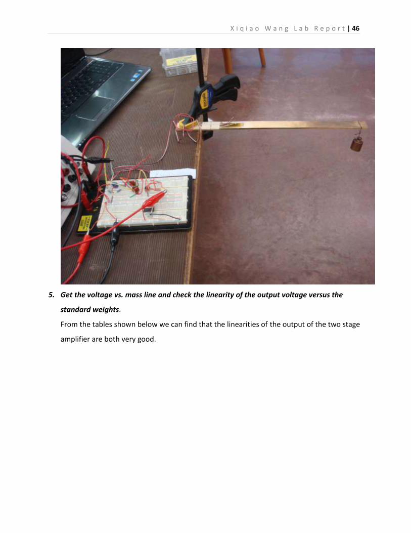
5. Get the voltage vs. mass line and check the linearity of the output voltage versus the
standard weights.
From the tables shown below we can find that the linearities of the output of the two stage
amplifier are both very good.

X i q i a o W a n g L a b R e p o r t | 47
6. Write LabView Programs
The main function of the program is to use the least square method to fit the straight line
by using the voltage output corresponding to standard weights. The formulas below are the
coefficients of the voltage-mass line V=am+b, and it’s correlation coefficient Rxy. Xs
represent the mass in gram of the standard weights and the Ys stand for the output voltage
of LM358 with the unit of voltage. The correlation coefficient is a measure of the
interdependence of two random variables that ranges in value from −1 to +1, indicating
perfect negative correlation at −1, absence of correlation at zero, and perfect positive
correlation at +1.

X i q i a o W a n g L a b R e p o r t | 48
where
.
In the LabView program, the first step is to input the voltage output and the corresponding
masses of standard weights into a two dimention array on the front penal, and then
through the index array function, add array elements function, formula function and
function node function, we get the squares of X, the products of Xi and Yi, and other
elements that composed to the formulas above, and arrange them in the display arrays.
Once we run the program, it will automatically calculate the coefficient a and b, and the
correlation coefficient r and display then in the front penal. The voltage input waveform will
be transformed to the waveform of mass and displayed in the waveform chart.

X i q i a o W a n g L a b R e p o r t | 49

X i q i a o W a n g L a b R e p o r t | 50

X i q i a o W a n g L a b R e p o r t | 51
Figure. 2

X i q i a o W a n g L a b R e p o r t | 52
Figure. 3
In Figure. 2, the correlation coefficient calculated according to the calibration data is
0.999962, which demonstrate an almost perfect positive correlation between the output
voltage and mass. The mass display shows 999.219g in response to a 1000g weight, which is
precise. From the waveforms shown above we can find that the strain gauge measurement
system is really sensitive that it can detect and clearly demonstrate the vibration of the
cantilever. Even the stand wave of the suspension line can be noticed in the mass waveform
chart. From the Figure. 3, because of the Mechanical Hysteresis, after having been loaded
for a period of time, the reading taken after no load was not zero as it should be.
7. Calculate the Young’s Modulus of Elasticity from the measurements
The method above to measure the weight using strain gauge is according to the fitting
linear equation. There is another method where we can get the weight under measurement
from the mechanics characteristics of the cantilever beam and the strain gauge. Firstly,
from the output voltage, we can calculate the change in gauge resistance based on the
structure of the bridge. Secondly, we can use the gauge factor of the strain gauge to
calculate the strain of the strain gauge, which is equal to the strain of the cantilever beam.

X i q i a o W a n g L a b R e p o r t | 53
Finally, the weight loaded on the bar will be decided by using the dimension parameters of
the beam and its Young’s Modulus.
V ∆R/R £ W
To achieve this goal, we should decide the Young’s Modulus first, thus we can know the
type of metal or alloy of the beam. The testing order will be reversed for the Yong’s
Modulus calculation.
Firstly, we use a known weight as a standard load, and measure the change of the strain
gauge resistance. Here we should take into consideration of the compensation of the
dummy strain gauge. Given the value of the gauge factor, we can get the strain. Thus the
Yong’s Modulus can be got from the equation below:
£=(6WL)/(Ebh²); Equation 1;
Where W is the weight in Pounds, L is the loading point’s distance from the mid-point of the
active gauge in inches, h is the thickness of the bar in inches, £ is the strain in Micro Inches.
Here, we applied 1000g weight as the load, and measured the change of resistances of both
active gauge and the dummy gauge. The original value of the active gauge resistance R3 is
120.414Ω, R3+∆R3 is 120.515Ω; the dummy gauge resistance R4 is 120.512Ω, and R4+∆R4 is
120.482Ω. So the actual resistance change of the active gauge caused solely by the strain is
∆R=∆R3-∆R4=0.131Ω. For G.F. equals 2.08, we got the strain was 523.04µ. Substitute the
Equation 1 with L=11.5”, d=1”, h=3/16”, I got the Young’s Modulus is 8.255*10⁶PSI.
8. Use Young’s Modulus and the parameters of strain gauge to measure the weight.
According to the circuit characteristics, the accurate calculation is easy to achieve as all the
resistance variables are measurable, but here we can assume that the zero-load resistance
of the four bridge arm are R= 120Ω. Then we get the approximate function below:
(∆R3-∆R4)/[4R+2(∆R3+∆R4)]*5V*10*99.13=V, since 2(∆R3+∆R4) is negligible in
comparison with 4R, the equation can be approximated as (∆R/4R)*4956.5=V.
Since W=(£Ebh²)/(6L), and £=∆R/(R*G.F.), W=(V*4*Ebh²)/(4956.5*2.8*6L)=1.2123*V.
The weight here is in Pound and the V here is the voltage directly sensed by SensorDAC in
Volt.
For LabVIEW program and universal application, the overall function is as follows:

X i q i a o W a n g L a b R e p o r t | 54
W=(Vout*4*E*b*h²)/(Vbridgesource*Gain*G.F.*6*L).
In the program of LabVIEW, the values in the front penal can be set as default values, where
the Young’s Modulus is 8.255*10^6, the length on the cantilever between the gauge and
the weight is 11.5 inches, the width of the cantilever is 1 inch, the thickness of the
cantilever is 3/16 inch, the bridge supply voltage is 5V, and the gauge factor of the strain
gauge is 2.08. The LabVIEW program according to the transfer function is shown below.

X i q i a o W a n g L a b R e p o r t | 55

X i q i a o W a n g L a b R e p o r t | 56
Reference
Nash, E. (June 1998). A Practical Review of Common Mode and Instrumentation Amplifier.
Peterborough: Helmers Publishing, Inc.
Saab, A. (2004, May 5). Experiments suggest methods for CMRR measurement. Sunnyvale:
Maxim Integrated Products Inc.

X i q i a o W a n g L a b R e p o r t | 57

X i q i a o W a n g L a b R e p o r t | 58

X i q i a o W a n g L a b R e p o r t | 59

X i q i a o W a n g L a b R e p o r t | 60

X i q i a o W a n g L a b R e p o r t | 61

X i q i a o W a n g L a b R e p o r t | 62

X i q i a o W a n g L a b R e p o r t | 63

X i q i a o W a n g L a b R e p o r t | 64

X i q i a o W a n g L a b R e p o r t | 65

X i q i a o W a n g L a b R e p o r t | 66

X i q i a o W a n g L a b R e p o r t | 67

X i q i a o W a n g L a b R e p o r t | 68

X i q i a o W a n g L a b R e p o r t | 69
Lab Report 3 Stepper Motor
Xiqiao Wang
E00340095
Abstract
This lab mainly involves the principles of stepper motor and its control system, analysis of the
driver circuits and the stepper motor signals, analog and digital output control of SensorDAQ,
and the application of window detector in combines with the strain gauge circuit built in
previous lab.
Equipment and materials
LM319N, SMD1 Stepper Motor Driver Kit, strain gauge circuit built in Lab2, Vernier SensorDAQ,
LabVIEW, Mitsubishi 42SH-32KCA stepper motor, Red Lion LMPC0000 magnetic sensor,
Oscilloscope, Multimeter, Power Sources, Function Generator.
Procedures
1. Stepper motor analysis.
Stepper motor is a brushless and synchronous electric motor that can divide a full
rotation into a large number of steps. In this experiment, the stepper motor in use has a
full step resolution of 1.8 degrees, which means the half step resolution is 0.9 degree.
Much higher precision can be achieved by the micro-steps input model.

X i q i a o W a n g L a b R e p o r t | 70
The big advantage of step motor is that it can be controlled precisely without feedback
mechanism as long as it is properly sized to the application and avoids skipping steps.
Therefore, counting pulses can be applied to achieve a desired amount of shaft rotation.
The count automatically represents how much movement has been achieved, without
the need for feedback information, as would be the case in servo systems. Whatever the
error that may be built into one step, it is noncumulative, so it can be almost negligible.
1.1. The type of stepper motor in use.
In this experiment, the stepper motor in use belongs to a hybrid type.
There are basically three types of stem motor. Permanent magnet motors use a
permanent magnet (PM) in the rotor and operate on the attraction or repulsion
between the rotor PM and the stator electromagnets. Variable reluctance (VR)
motors have a plain iron rotor and operate based on the principle that minimum
reluctance occurs with minimum gap, hence the rotor points are attracted toward
the stator magnet poles. Hybrid stepper motors are named because they use a
combination of PM and VR techniques to achieve maximum power in a small
package size. Modern steppers are of hybrid design, having both permanent
magnets and soft iron cores.
1.2. Unipolar two-phase stepper motor.
The two phase stepper motor is the one that is mostly used. There are two basic
winding arrangements for the electromagnetic coils: bipolar and unipolar. The
stepper motor used in this assignment is unipolar.
A unipolar stepper motor has two windings per phase, one for each direction of
magnetic field. Since in this arrangement a magnetic pole can be reversed without
switching the direction of current, the commutation circuit can be made very simple
(e.g. a single transistor) for each winding. Typically, given a phase, one end of each

X i q i a o W a n g L a b R e p o r t | 71
winding is made common: giving three leads per phase and six leads for a typical
two phase motor.
The torque output of the unipolar wound motor is lower than the bipolar motor (for
motors with the same winding parameters) since the unipolar motor uses only 50%
of the available winding while the bipolar motor uses the entire winding.
1.3. Distinguish the common wire from the coil-end wires.
The way to distinguish common wire from a coil-end wire is by measuring the
resistance. Resistance between common wire and coil-end wire is always half of
what it is between coil-end and coil-end wires. This is because there is twice the
length of coil between the ends and only half from center (common wire) to the end.
There are 6 leads of different colors coming out of the stepper motor in this
experiment. By detecting the resistances between any combination of two wires, I
got that the red and brown wires are the windings of one phase, the resistance
between them is 122.75Ω, the white lead is their common wire and the resistance
between the red and the white wire is 61.84Ω. The blue wire and yellow wire are
the windings of the other phase and the black lead is their common wire. The wires
between different phases have a typically infinite resistance value.
Another quick method to distinguish which leads belong to which phase is to short
the circuit every two pairs and try to turn the shaft. Whenever a higher than normal
resistance is felt, it indicated that the coil-end leads to the particular winding are
connected. The reason is that when the coils are formed into closed loops, when the
permanent magnet rotor moves, the magnetic flux through the coils changes, the
changing rate of the magnetic flux determines the induced electromotive force
generated in the coils. Since the coils form closed loop circuits, there are induced
currents running through the coils in the direction that the magnetic field generated
by them will reject the motion of the rotor.
1.4. The control wave forms of the stepper motor (applicable for both bipolar mode
and unipolar mode).
1.4.1. Full step mode.

X i q i a o W a n g L a b R e p o r t | 72
For the stepper motor under use in this assignment, the phases can be
energized one at a time, thus the rotor will rotate in increments of 1.8
degrees and in each step while the nearest teeth of the gear shaped PM
rotor will align to the energized stators and the rotor teeth near the other
phase will be slightly offset from the teeth of the stators.
This motor can also be driven two wings at a time and yield more torque. The
simplified scheme and signal sequence are shown below. Assume that A and
B stand for the two phases, which is also called two poles, of the stepper
motor, and the numbers stand for two windings of the same coil in the
unipolar two-phase stepper motor.
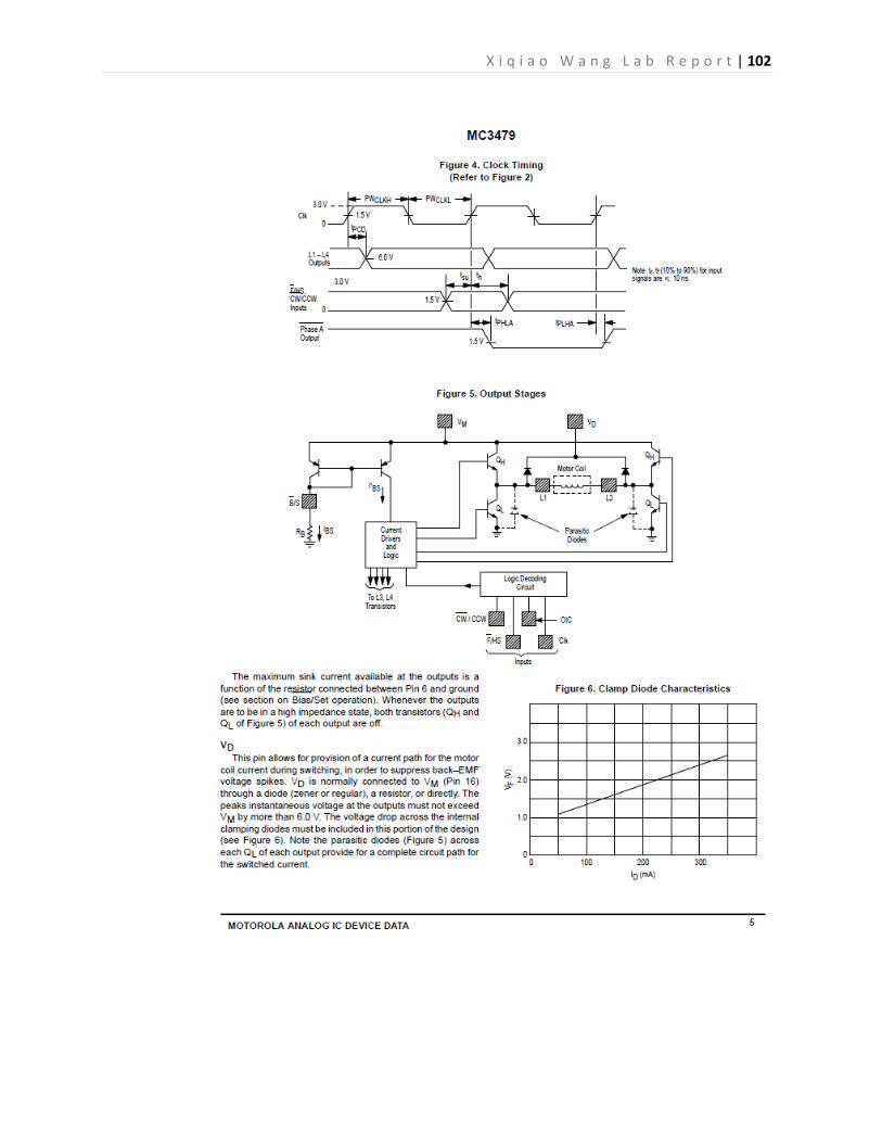
The MC3479 output sequence is shown below when it is in full step mode
when the input at the Full/Half pin is at a logic “0” (<0.8V). The output
sequence direction determines the rotation direction of the motor. The
Phase A condition is defined as L1 and L3 are at output high driver voltage, L2
and L4 are at output low driver voltage.

X i q i a o W a n g L a b R e p o r t | 73
1.4.2. Half step mode.
Greater resolution can be gained if the motor is rotated half a step at a time.
If this mode is selected less torque is generated by the motor. There is less
torque because for every half step only one magnet pair is attracting the
magnet connected to the shaft. Half steps are created by turning off one pair
of poles in between transitions from one step to another. The sequence for
switching the poles in a half step mode is displayed below.

X i q i a o W a n g L a b R e p o r t | 74
Below are the MC3479 output sequences when it is at half step mode and
the output impedance control (OIC) pin is grounded, as the SMD1 stepper
motor controller schematic diagram has showed in the next report section.
When the outputs are in Phase B, D, F or H, the two outputs to the de-
energized coil are in a high impedance condition, which means the transistor
QL and QH of both the outputs of the de-energized coil are off. When the OIC
input is at a logic “1” (>2V), a low impedance output is provided to the de-
energized coil as both outputs have QH on and QL off. For the detailed
controller analysis, refer to the controller circuit analysis in the next report
section.
2. Construct the Stepper Controller and Circuit Analysis.

X i q i a o W a n g L a b R e p o r t | 75
As the schematic diagram and the datasheet indicated that Pin1 of MC3479 is inner connected
with the four camp diodes’ cathodes, it is easy for the reader to be misguided that there are
four negative clamp circuits are equipped with a bias DC voltage,which is added between the
diodes and ground, offset the output voltage by that amount. In fact, from the diagram after,
we can see that the clamp circuit is much simpler that the ones using capacitor and diode. As
indicated in the datasheet the function of Pin1, which is used to protect the outputs where
large voltage spikes may occur as the motor coils are switched, the clamp diode connected to
each output is to limit the spikes from the coils to within 2.5V above the Vd voltage. From the
SMD1 schematic diagram, the Vd pin of MC3479 is connected to the DC voltage supply through
two diodes, which also clamp the voltage input of Vd about 1.5V above the power supply
voltage. This design meets the maximum Vd voltage in the MC3479 Datasheet, which is VM+5V,
and it is within the recommended Clamp Diode Cathode Voltage from VM to VM+4.5V. Because
the typical voltage drop across the clamp diode at the output is 2.5V, the coil spikes are limited
to VM +4 v, which ensure the safety of the chip.
From the Output Stage diagram of MC3479, the current driver and logic output small current to
satirize either the transistor QH or QL to decide the output voltage. The transistor can provide
enough output current directly from the power supply.

X i q i a o W a n g L a b R e p o r t | 76
The circuit with the Bias/Set output composed of a mirror current source that the current input
into the Current Drivers and Logic will always equal to the current out of the Bias pin. And the
current of the current drive will decide the base current of the QH and QL transistor, thus
determine the maximum output sink current. The function of the maximum output sink current
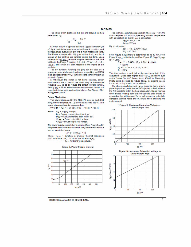
is IBS=IOD*0.86, where IBS is the base drive current supplied to the lower transistor QL in micro
amps and IOD is the coil current in milliamps.
The method of the SMD circuit to limit the current supplied to the motor coil is achieved by
forming and initialing a jumper wire in the 6-pin Molex connector in the low power position. A
5V voltage supply is connected to the Phase A output and thought the low power jumper
connected to NAND U2:C. The high input cause the NAND to give a low level output when the
RUN button is on. This allows a small base current for Q2 and a small collector current which
decide the value of the Bias/Set current.
The Pin10 of MC3479 is the output impedance control and its function may be useful in further
applications. This input is relevant only in the half step mode (Pin 9 > 2.0 V). When low (Logic
“0”), the two driver outputs of the non–energized coil will be in a high impedance condition.
When high the same driver outputs will be at a low impedance referenced to VM.
For the peripheral circuit, the circuit is mainly composed of the Oscillator section and the
control section. The oscillator section use RC circuit to generate the clock signal of MC3479.
We can change to speed of the turning shaft be input other clock signals through Jumper 2. In
the control section, RUN button connects to NAND U2:D, which enable the clock output when
RUN is on. It also connects to NAND U2: C and transistor Q1, and enable the bias current input
when RUN is on. If the Bias/set pin is opened (IBS < 5.0 mA) the outputs assume a high
impedance condition, while the internal logic presets to a Phase A condition.

X i q i a o W a n g L a b R e p o r t | 77
3. The typical stepper motor system.
The typical stepper motor system is composed of computer, microprocessor or PLCs
that generates commands according to different conditions. It sends the commands to
the indexer whose function is to create the clock pulses, direction control and state
control. The signals are sent to a stepper motor driver to directly drive the stepper
motor. In this assignment, the LabView program and SensorDAQ interface would be the
computer part. SMD1 stepper motor driver kit combines the indexer and driver together.

X i q i a o W a n g L a b R e p o r t | 78
4. Drive circuit analysis.
The basic electric characteristic of the winding of each phase in the stepper motor is the
inductance and the equivalent resistance. The resistance of the winding is responsible
for the major share of the power loss and heat up of the motor. The power loss of the
resistance in the motor is given by the function below:
PR=R*I²;
It is worth to mention that the motor should be used at its maximum power dissipation
to be efficient, that it to be used in its maximum current level. Such consideration is
mainly from the cost efficient perspective in the industry application.
The inductance makes the motor winding oppose current changes, which is to impede
the current from increasing when the winding is charged and to impede the current
from decrease when the winding is de-energized. The inductance limits the high speed
operation of the stepper motor. The figure below shows the electrical characteristics of
an inductive–resistive circuit. When a voltage is connected to the winding the current
rises according to the equation
I(t) = ( V ⁄ R )* ( 1 – e^(– t * R ⁄ L) );
Initially the current increases at a rate of dI⁄dt (0) = V ⁄ L. The rise rate decreases as the
current approaches the final level: IMAX = V ⁄ R. The value of te = L ⁄ R is defined as the
electrical time constant of the circuit. The te is the time until the current reaches 63% ( 1
- 1⁄e ) of its final value.

X i q i a o W a n g L a b R e p o r t | 79
5. Stepper motor voltage signal analysis in the situation of (unipolar) misuse and normal
(bipolar) use.
I made two mistakes at the beginning of my experiment. The first is that I did not notice
that the MC3479 chip is designed to drive a two phase stepper motor in the bipolar
mode. I mistakenly connect the center pads of the coils to the ground and construct a
unipolar mode. The second mistake is that I detected the stepper motor voltage signals
instead of the current signals which determine the actual performance of the stepper
motor. Though analysis, I had figured out how to explain the mistakenly recorded
voltage signals.

X i q i a o W a n g L a b R e p o r t | 80
A. Stepper motor unloaded at maximum speed. B. Stepper motor loaded at maximum
speed.
Connect the probe of
the oscilloscope at L1.
Mistakenly connect the center
tap to the ground.
X i q i a o W a n g L a b R e p o r t | 81
C. Stepper motor overloaded at maximum speed. D. Without motor at maximum
speed.
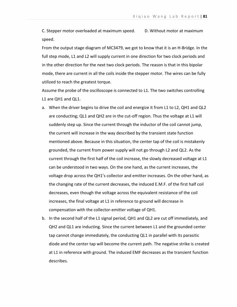
From the output stage diagram of MC3479, we got to know that it is an H-Bridge. In the
full step mode, L1 and L2 will supply current in one direction for two clock periods and
in the other direction for the next two clock periods. The reason is that in this bipolar
mode, there are current in all the coils inside the stepper motor. The wires can be fully
utilized to reach the greatest torque.
Assume the probe of the oscilloscope is connected to L1. The two switches controlling
L1 are QH1 and QL1.
a. When the driver begins to drive the coil and energize it from L1 to L2, QH1 and QL2
are conducting; QL1 and QH2 are in the cut-off region. Thus the voltage at L1 will
suddenly step up. Since the current through the inductor of the coil cannot jump,
the current will increase in the way described by the transient state function
mentioned above. Because in this situation, the center tap of the coil is mistakenly
grounded, the current from power supply will not go through L2 and QL2. As the
current through the first half of the coil increase, the slowly decreased voltage at L1
can be understood in two ways. On the one hand, as the current increases, the
voltage drop across the QH1’s collector and emitter increases. On the other hand, as
the changing rate of the current decreases, the induced E.M.F. of the first half coil
decreases, even though the voltage across the equivalent resistance of the coil
increases, the final voltage at L1 in reference to ground will decrease in
compensation with the collector-emitter voltage of QH1.
b. In the second half of the L1 signal period, QH1 and QL2 are cut off immediately, and
QH2 and QL1 are inducting. Since the current between L1 and the grounded center
tap cannot change immediately, the conducting QL1 in parallel with its parasitic
diode and the center tap will become the current path. The negative strike is created
at L1 in reference with ground. The induced EMF decreases as the transient function
describes.

X i q i a o W a n g L a b R e p o r t | 82
c. The analysis above does not take the mutual inductance between the two wings of
the same coil into consideration. Besides, the difference between the L1 waveforms
when the motor is at its maximum and minimum speed is caused by whether the
current through the wings reach its maximum value or not. When the clock
frequency is high, there is not enough time for the inductor’s current increase to its
full range. The voltage waveforms at the lowest speed are shown below.
A. Stepper motor unloaded at minimum speed. B. Without motor at minimum
speed.
d. The following voltage waveforms capture the interruptions when the stepper motor
is overloaded.

X i q i a o W a n g L a b R e p o r t | 83
Figure. Torque vs. rotor angular position. Figure. Torque vs. speed characteristics.
When the motor is overloaded, it should be considered operating at the start/stop
region. The Pull-in curve is the maximum frequency at which the motor can start or stop
instantaneously without loss of synchronism. When overloaded, the motor start to lose
steps. But the frequency of the clock input is a constant, which means the start rate is
fixed while the load force is greater than the maximum torque the motor can provide at
the corresponding frequency. This torque is less than the holding torque TH showed in
the left figure. The decreasing torque output as the speed increases is caused by the
fact that at high speeds the inductance of the motor is the dominant circuit element.
The torque vs. angle characteristics of a stepper motor is shown as above. An ideal
stepper motor has a sinusoidal torque vs. displacement characteristic. A and C Positions
represent the stable equilibrium points when no external force or load is applied to the
rotor shaft. We can assume the holding torque TH showed in the sinusoidal curve
represents the maximum torque when the motor is in motion at a specific speed rate.
When the motor is loaded but not overloaded, the motor shaft will have an angular
displacement. This angular displacement is referred to as a lead or lag angle depending
on whether the motor is actively accelerating or decelerating. When the motor is
overloaded, the load force is greater than the maximum torque. The motor will not able
to rotate the shaft to reach an angular displacement corresponding to the maximum
torque. The shock pulse is generated when the torque provided by the stepper motor
reach the TH, but because the load force prevent the shack to have a rotation of ¼ step

X i q i a o W a n g L a b R e p o r t | 84
angle. As the torque begin to decrease after TH, the shaft return to its blocked position
quickly. Because the shaft is made of permanent magnet, the sudden change of the
magnetic field inside the coils generates the induced EMF demonstrated as the shock
pulse voltage.
e. The stepper motor signal wave form in normal use.
In the correct connection situation, the center taps of the 6-wire stepper motor
should be disconnected from ground. The voltage waveform at the stepper motor’s
pin is shown below. The analysis of the waveform is similar to that that above.
Figure. Bipolar stepper unloaded and overloaded at maximum speed.
Figure. Bipolar stepper unloaded and overloaded at minimum speed.
6. Build a Bang-Bang controller.
X i q i a o W a n g L a b R e p o r t | 85
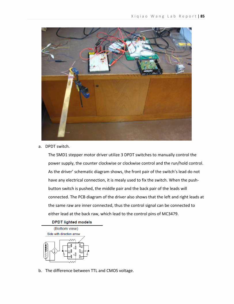
a. DPDT switch.
The SMD1 stepper motor driver utilize 3 DPDT switches to manually control the
power supply, the counter clockwise or clockwise control and the run/hold control.
As the driver’ schematic diagram shows, the front pair of the switch’s lead do not
have any electrical connection, it is mealy used to fix the switch. When the push-
button switch is pushed, the middle pair and the back pair of the leads will
connected. The PCB diagram of the driver also shows that the left and right leads at
the same raw are inner connected, thus the control signal can be connected to
either lead at the back raw, which lead to the control pins of MC3479.
b. The difference between TTL and CMOS voltage.

X i q i a o W a n g L a b R e p o r t | 86
The two families utilize different types of transistors in their construction, Bipolar
Junction transistors for TTL and Field Effect Transistors are used for the CMOS. There
are various types of both transistors, but one common way to categorize them is
whether they are N or P devices, NPN and PNP for bipolar and NMOS and PMOS for
the CMOS, where the N and P refers to the element used to dope the silicon. The
MOS stands for Metallic Oxide Semiconductor, which is a very thin high valued
insulator that is used to create the very low input current of CMOS devices. The C in
CMOS stands for complementary, which means that both N and P transistors have
been fabricated together to implement the logic. This allows the rail to rail 0 - 5 volt
output swings achievable with CMOS.
A bipolar transistor can be considered as a current driven switch where the FET can
be viewed as a voltage controlled switch. This factor comes into play in that it is
responsible for the different HIGH and LOW logic voltages and influences how and
when TTL and CMOS devices can be connected together. To control TTL circuit,
enough current supply ability should be taken into consideration instead of only the
voltage level, even though the required voltage level is the prerequisite to generate
enough current.
Specifically, for TTL input, the voltage less than 1.2V is considered low input level,
and the voltage that is greater than 2.0V is considered high level input voltage. For
the TTL output voltage, the voltage that is less than 0.8V is considered as low level
output voltage, and the one that is greater than 2.4V is considered as high output
voltage. The voltages between the upper and lower limits are considered invalid
voltages. For the CMOS circuit, the low level input voltage is less than 0.3*Vcc and
the high level input voltage is greater than 0.7*Vcc. The CMOS low level output
voltage is less than 0.1*Vcc and the high level output voltage is greater than 0.9*Vcc.
From the perspective of current, TTL circuits can drive CMOS circuits. From the
perspective of voltage, CMOS circuits can drive TTL circuits. A lot of circuits choose
5V as DC power supply so that the circuits will be compatible for both TTL and CMOS

X i q i a o W a n g L a b R e p o r t | 87
circuits. There will always be a TTL-CMOS compatible buffer between the input and
the inner circuit.
c. Build Window Detector.
The MC3479 is designed to have TTL/CMOS compatible inputs, which results to the
input voltage for logic control is limited to 0V to 5.5V. The low-to-high input
threshold is 2.0V and the high-to-low input threshold is 0.8V. It can be inferred that
a 5V regulator IC is built inside MC3479.
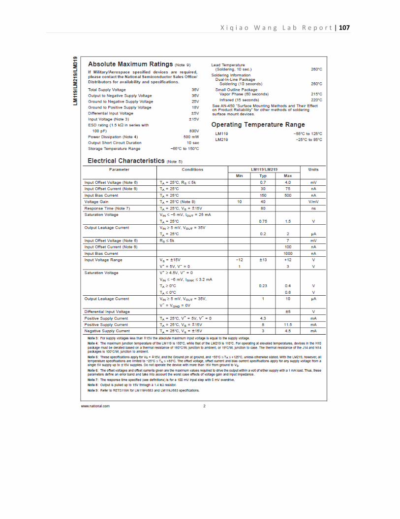
The comparator chip used in this assignment is LM319N, which is a typical TTL circuit.
The inner structure of LM319N is shown as below.
The uncommitted collector of the output stage makes LM319N compatible with RTL,
DTL and TTL as well as capable of driving lamps and relays at currents up to 25mA by
connect by choosing proper output stage voltage supply and current-limiting
resistance. If the an output current greater than 25mA is needed, another stage of
transistor can be used by choosing proper model of power transistor. The practical
application of the comparator output as MC3479’s logic input do not have problems
without using an extra current amplify transistor.
The window detector’s principle circuit is shown below. Multisim simulation is
conducted before building the real comparator circuit.
Open Collector output structure of
LM319N.
If the output voltage of the comparator has difficulty to go
back to low level sometimes, usually the problem should be
located to a bad ground connection at the output stage of the
comparator.

X i q i a o W a n g L a b R e p o r t | 88
From the principle of comparator, when the voltage at inverting input is less than
the voltage at non-inverting input, the output will be high, which means the output
stage transistor is cutoff. Then the inverting voltage is greater than the non-inverting
voltage, the output stage transistor will be saturated and it is conducting. Both
comparators will have high outputs when the applied voltage is between the upper
and lower limits, then the overall output will be high since both comparators are
cutoff. When the applied voltage is above the upper limit or below the lower limit,
one of the comparator will be conducting and pull the output voltage down. The

X i q i a o W a n g L a b R e p o r t | 89
current limit resistance is used to limit the current going thought the output stage
transistor under 25mA.
In this assignment, I use the strain gauge circuit, and set the Bang-Bang as from 500g
to 1600g. If I use the output of the LM358 as the application voltage of the window
detector, the window voltage will be from around 1V to about 1.5V. So I set the limit
voltages by using potentiometers. The real circuit connection is shown below. The
oscilloscope screen captures after it show the changing process of the window
detector’s output as the weight applied on the strain gauge increases. Note: the
yellow line is the window detector output, and the blue line is the strain gauge
voltage output. We can see that the low level of the window detector output is 0.4V,
and the high level is about 5V. One thing needs to pay attention is that all the
separate section circuits should be common grounded. Since the stepper motor
driver chip MC3479 is compatible for both TTL and COMS input, and MC3479 used
5V as its voltage supply, as long as the input voltage satisfy the CMOS voltage
standards, again, there is no need to connect an extra transistor between the
stepper motor driver kit and the comparator.

X i q i a o W a n g L a b R e p o r t | 90
(1). The output is low. (2). The output is high.
(3). The output is low again.
Some problems were encountered when the input of the window detector went
down through the lower bang of the window. Sometimes, the high level output of
the window detector would not go down to low level output, and alight adjustment
of the ground connection will solve the problem. This problem could be traced back
to a bad grounding of the one of the two comparators U2B shown in the Multisim
diagram.
d. The transfer function of the Bang-Bang controller.
The original input of the Bang-Bang controller, which is composed of the strain gauge
circuit, the window detector circuit and the stepper motor driver circuit, is the weight
loaded on the cantilever, and the ultimate output of the Bang-Bang controller are the
different motion properties of the stepper motor. For the strain gauge circuit, the
transfer function between the output voltage and the loaded weight is shown as
follows (See Lab Report 2 for details):

X i q i a o W a n g L a b R e p o r t | 91
W=(Vout*4*E*b*h²)/(Vbridgesource*Gain*G.F.*6*L).
Vin<1V when W<500g;
1V<Vin<1.5V when 500g<W<1600g;
1.5V<Vin when 1600g<W.
Where W is the weight in Pounds, L is the loading point’s distance from the mid-point
of the active gauge in inches, h is the thickness of the bar in inches, £ is the strain in
Micro Inches, E is Young’s Modulus in PSI, G.F. is the gauge factor.
The transfer function of the window detector is:
Vwin=5V when 1V<Vin<1.5V;
Vwin=0V when Vin<1V or Vin>1.5V.
If the output of the window detector is used to control the rotate direction of the
stepper motor, then the overall transfer function would be as follows.
Motor direction=CW when 500g<W<1600g;
Motor direction=CCW when W<500g or W>1600g.
7. Connect the magnetic sensor.
The logic magnetic pickup used in this assignment is the red lion LMPC0000. It will sense
the approach of ferrous targets. The one in use is a type of NPN Open
Collector Transistor Output unit which provides a negative going current sinking
output with the approach of a ferrous target and is current limited to 40 mA. We only
need to connect a resistor between the voltage supply line and the output signal line as
the current limiting resistor. The supply voltage ranges from 9V to 30V. Since the
SensorDAQ’s analog input voltage ranges from -10V to +10V, the LMPC0000’s supply
voltage is chosen to be 9V. The counter pulse will be negative pulses below 9V.

X i q i a o W a n g L a b R e p o r t | 92
Since the voltage supply range of the magnetic sensor is from 9VDC to 30VDC, the
negative pulse detected by the analog input of the SensorDAQ is shown below. To use
the Counter/Timer pin PFI0 of the sensorDAQ to realize the function of the event
counting, it is better to inverse the negative pulses and reshape the pulses as square
wave pulses to increase the accuracy of the event counting. I decided to use LM319N to
build the comparator.
From the datasheet of LM319, under the condition of V+=5V and V-=0V, the input
voltage range is from 1V to 3V, and the input differential voltage range has a maximum
value of ±5V, so a potentiometer was needed to divide the magnetic sensor output
voltage. The Multisim diagram is shown below. The output of LMPC0000 was divided by
the potentiometer R2 and connected with the non-inverting input of LM319N. Then set
the inverting input of LM319N. The wave form is shown below.

X i q i a o W a n g L a b R e p o r t | 93
Figure7.1. A bang (blue) and the attenuated LMPC0000 signal.
Figure7.2. The output of the comparator (blue) became positive pulse with an amplitude
of 5V.

X i q i a o W a n g L a b R e p o r t | 94
Figure7.3. Non-ideal counter pulse input.
The output signal of the comparator can be connected with the PFI0 pin of SensorDAQ,
and the event counting LabVIEW program is shown below. The program referred to the
VI example “Terminal_CounterCounting”. The counter feature allows us to command
screw terminal 7 (PFI 0) to perform simple event counting. Here, to measure the RPM of
the stepper motor, I set the Count Interval as 0.1, which means at the end of every
single 0.1s, the new count number would be demonstrated, ran the program for one
minute, the count number would be the RPM. In some cases, the counter pulse will not
be an ideal square waveform due to vibrations as shown in Figure7.3. , proper threshold
should be set in the LabVIEW program to ensure the event counting not to skip.

X i q i a o W a n g L a b R e p o r t | 95
8. Use SensorDAQ to control the stepper motor driver kit.
The basic principle of this step is to use the digital output function of SensorDAQ to
replace the switches mounted on the SDM1 driver kit. From the SensorDAQ
specification, the digital I/O has a compatibility of TTL, LVTTL and CMOS, there is no
need to add extra transistor between MC3479 and screw terminals. The LabVIEW
program is shown as follows. This program referred to the VI example
“Terminal_DigOut.vi”. The four digital output lines can be controlled in the front penal.
Respectively, the first button controls the Run/Hold function; the second button
controls CW/CCW function; and the third button controls the Full/Half step function.
The forth button is reserved.

X i q i a o W a n g L a b R e p o r t | 96

X i q i a o W a n g L a b R e p o r t | 97

X i q i a o W a n g L a b R e p o r t | 98

X i q i a o W a n g L a b R e p o r t | 99

X i q i a o W a n g L a b R e p o r t | 100

X i q i a o W a n g L a b R e p o r t | 101
X i q i a o W a n g L a b R e p o r t | 102

X i q i a o W a n g L a b R e p o r t | 103
X i q i a o W a n g L a b R e p o r t | 104

X i q i a o W a n g L a b R e p o r t | 105

X i q i a o W a n g L a b R e p o r t | 106
X i q i a o W a n g L a b R e p o r t | 107

X i q i a o W a n g L a b R e p o r t | 108

X i q i a o W a n g L a b R e p o r t | 109

X i q i a o W a n g L a b R e p o r t | 110

X i q i a o W a n g L a b R e p o r t | 111
X i q i a o W a n g L a b R e p o r t | 112

X i q i a o W a n g L a b R e p o r t | 113

X i q i a o W a n g L a b R e p o r t | 114

X i q i a o W a n g L a b R e p o r t | 115
ENTC4277 Lab Report 4 Vibration Measurement
Part1. Use Balmac Vibration Transmitter to measure vibration
Equipment
SensorDAQ, LabVIEW, Balmac Mode 191 Series Vibration Sensor, electric fan, resistor.
Procedures
From the datasheet of Balmac Mode 191 Series Vibration Sensor, we got to know that the one under
our use is Mode 191-2, whose measurement range of linearity is from 1 in/sec to 2 in/sec. The
corresponding output range is from 4mA to 20mA, which is proportional to the overall vibration. An
output of 4mA indicates 0 in/sec or no vibration while an output of 20mA indicates the maximum full
scale range is present. In reality, the maximum output current value is 110mA, but for the output
current larger than 20mA, the relation between the output current and the vibration level is no longer
linear.
The Balmac 191 sensor has a two-wire, loop powered structure. The circuit diagram is shown above,
where the two leads of the vibration sensor are in series with a resistor load and DC voltage power. The
voltage drop across the resistor is used as the input signal of SensorDAQ. One point need to be noticed
is that the maximum analog input voltage range of SensorDAQ is ±10V, so for the linear current range
from 4mA to 20mA, the load resistance value should be less than 500Ω. On the other hand, the
resistance value should be large enough to ensure a large enough voltage signal for measurement and
signal processing.
Vibration measurement locations shall be on the rigid member if the machine, as close to each bearing
as feasible. For the vibration measurement of a fan, the transmitter should be mounted on the bearing

X i q i a o W a n g L a b R e p o r t | 116
rod or on the enclosure of the shaft of the electric motor, instead of the cover or the guard that is
flexible or dismountable. For a comprehensive vibration measurement, axial, vertical and horizontal
vibration measurement should be conducted. But since the current lab conditions do not allow us to
firmly mount the Balmac sensor to the ideal locations of the fan, we attach the sensor to the cover of
the fan using scotch tape.
Program designed using LabVIEW is shown below. Use Analog Express to measure the voltage input, and
convert the signal to current in milliamp. According to the linear relation of vibration vs. current, the
vibration level is easy to get. The compare functions are used to set alarm thresholds. Here, 0.3 in/sec is
set as lower threshold, and 1 in/sec higher threshold. For the condition where the Balmac sensor is
mounted parallel to the rotator of the fan, SensorDAQ measurement results are shown below.

X i q i a o W a n g L a b R e p o r t | 117
Figure. For low fan speed.
Figure. For medium fan speed.
Figure. For high fan speed.

X i q i a o W a n g L a b R e p o r t | 118
Figure. ISO standard 2372-1974.
According to ISO standard 2372-1974, if the fan is classified as small machine, its vibration level will be
considered as unacceptable since its vibration levels at all three speeds are greater than 0.4 in/sec.
Besides, we can use the digital oscilloscope’s FFT analysis function to find clues about the shaft’s RPM,
even though Balmac’s output is merely DC current signals. If we assume the second highest peak
represent the shaft’s RPM, then, approximately, the low fan speed is 18 RPM, the medium fan speed is
26 RPM and the high fan speed is 30 RPM.

X i q i a o W a n g L a b R e p o r t | 119
Figure. FFT analysis for low fan speed.
Figure. FFT analysis for medium fan speed.

X i q i a o W a n g L a b R e p o r t | 120
Figure. FFT analysis for high fan speed.
Part. 2 Use Endevco Model 256-100 accelerometer to measure vibration
Equipment
Endevco Model 256-100 Accelerometer, SenserDAQ, CR300 Current Regulator diode, LabVIEW,0.01µF
capacitor, T Junction Connector, Digital Oscilloscope.
Procedures
1. Endevco Accelerometer analysis
Figure. Inner structure of piezoelectric accelerometer
An accelerometer measures proper acceleration, which is the acceleration it experiences relative to
free-fall and is the acceleration felt by people and objects. Put another way, at any point in space-time
the equivalence principle guarantees the existence of a local inertial frame, and an accelerometer
measures the acceleration relative to that frame. Such accelerations are popularly measured in terms of
g-force. An accelerometer at rest relative to the Earth's surface will indicate approximately 1 g upwards,
because any point on the Earth's surface is accelerating upwards relative to the local inertial frame (the
frame of a freely falling object near the surface). To obtain the acceleration due to motion with respect
to the Earth, this "gravity offset" must be subtracted and corrections for effects caused by the Earth's
rotation relative to the inertial frame. But the Endevco accelerometer we used in this experiment is a
dynamic accelerometer, which means it is only sensitive to the acceleration of dynamic motion in
respect to earth. The reason is that it is a piezoelectric accelerometer; the piezoelectric material used
inside the accelerometer will generate equal amount of opposite electric charge when external force is
applied and deformation occurs. Here, the piezoelectric material is considered the dielectric medium of

X i q i a o W a n g L a b R e p o r t | 121
the capacitor, and leakage of electric charge on the two plates is unavoidable. Besides, the load of this
piezoelectric capacitor, which is the amplifier/impedance converter circuit, will also compose of a
discharging loop. Thus with the two paralleled discharging loops, the charges generated on the opposite
plates cannot be kept for a static measurement. This is why the Endevco accelerometer will not
demonstrate a static signal of the gravitational force when it is perpendicular with the horizontal plane.
It is only suited to dynamic measurement.
Most micromechanical accelerometers operate in-plane, that is, they are designed to be sensitive only
to a direction in the plane of the die. By integrating two devices perpendicularly on a single die a two-
axis accelerometer can be made. By adding an additional out-of-plane device three axes can be
measured. Such a combination always has a much lower misalignment error than three discrete models
combined after packaging.
Due to the low output signal and high output impedance that piezoelectric accelerometers possess,
there is a need for amplification and impedance conversion of the signal produced. In the past this
problem has been solved using a separate (external) amplifier/impedance converter. This method,
however, is generally impractical due to the noise that is introduced as well as the physical and
environmental constraints posed on the system as a result. Today IC amplifiers/impedance converters
are commercially available and are generally packaged within the case of the accelerometer itself.
In practice, even though the Endevco accelerometer we use has an imbedded IC amplifier/impedance
converter, electromagnetic interference still cannot be eliminated as is shown in the figure below. In this
occasion, the accelerometer was hold statically and was not mounted to any mechanical vibration
surface, but a 60Hz voltage signal was still detected from the voltage output of the accelerometer. The
EMI might be from the running fan or other electric devices and was probably introduced from the
accelerometer’ long transmission line.

X i q i a o W a n g L a b R e p o r t | 122
Figure. Electromagnetic noise signal detected when the accelerometer is static.
2. CCD connection.

X i q i a o W a n g L a b R e p o r t | 123
Figure. Circuit connections.
From the power requirement of Endevco 256-100, we get to know that that the DC power supply
voltage should be between 18V and 24V, and the supplied current should be limited between 2mA to
10mA. We apply a CCD (constant current diode) in series with the power supply. The CCD we used in this
circuit is CR300 which has a typical constant current of 3mA. The schematic diagram and the V-I
characteristics of the CCD connection is shown below. When the voltage across the CCD is greater than
its forward bias voltage (build-in potential), the CCD break-overs in the forward direction and keeps the
current flowing throw it almost unchanged with the voltage changing within certain voltage range.
When the voltage is reversely across the CCD, it will not regulate the current and the current will
increase dramatically as the voltage increases. The CR300 we used in this lab has peak operating voltage
of 100V and absolute maximum reverse current of 50mA.
Apply a 0.01µF ceramic in
capacitor in series with the
readout device input.

X i q i a o W a n g L a b R e p o r t | 124
Figure. Constant Current Diode CR300.
Because the Endevco accelerometer in use is really expensive, before connecting it into the circuit, it is
necessary for us to check the valibility of the constant current diode. We connect a resistor in series with
the voltage supply and the CCD, change the voltage supply value and examine the voltage drop across
the resistor, and then calculate the current in this circuit. It is worth mentioning that the anode of the
CCD is the one near the outthrust of the iron cap.
3. DC blocking circuit analysis.

X i q i a o W a n g L a b R e p o r t | 125
The equivalent circuit of the Endevco accelerometer application circuit can be considered as
shown above. Here, I consider the piezoelectric material and the capacitor plates across it as a
capacitor Ca in series with a AC voltage source V1. The equivalent insulation resistance of the
crystal is equivalent as Ra. Since the amplifier/impedance converter is integrated inside the
sensor, the equivalent capacitance of the cable Cc between piezoelectric material and the
imbeded amplifier can be omitted. Ri and Ci are the equivalent input resistance and capatance
of the build-in amplifier U1. Ro and Co are the output resistance and capacitance of the build-in
amplifier U1. Ccable is the equivalent capacitace of the accelerometer’s connection cable; it
cannot be ommited because this cable is long and easy to be affected by the electromagnetic
interferences in the environment. V2 is the DC voltage supply, supplying DC voltage through the
CCD. A T-Junction connector is utilized to combine the voltage supply, signal output and
SensorDAQ analog input together at node 1. Capacitor C and resistor R are used to compose a
high-pass filter (HPF) to block the DC output bias voltage of the accelerometer. R4 and C6 are
the input equivalent resistance and capacitance of the SensorDAQ analog input.
According to the Endevco datasheet, for Model 256-100’s voltage sensitivity of 100mA/g, the
typical amplitude response is from 1Hz to 9000Hz. Thus the resistance and capacitance values
inside the accelerometer are desided accordingly to have a proper time constant that should be
large enough to have a good low frequency response.
On the other hand, from the specification, we got to know that the input impedance of the
SensorDAQ analog input is greater than 1MΩ. The bias current and the equivalent capacitance
of the analog input is not mentioned in its specification. As a high frequency filter, its time
constant should be as large as possible so that its cut-off frequency can be as close as DC, thus
minimize the DC blocking circuit’s effects on the low frequency component of the viberation
signals. The resistance value R in the high-frequency filter should be chosen carefully. Because it
not only desides the time consistant and cut-off frequency, but also acts as a bleeder resistance
if the SensorDAQ analog input has a bia current. To decrease the cut-off frequency, this R value
should be the larger, the better. But if it is too large, then the charges accumulated at the
capacitors negative plate cannot be bleeded on time, thus causing a DC voltage component the
DC blocking circuit.
I think the reason why we detected a 1.42V DC voltage after out DC blocking circuit in our
experiment is probably due to the SensorDAQ analog input bias current. In our experiment
circuit, we used a 0.01µF ceramic capacitor, and considered the analog input equivalent

X i q i a o W a n g L a b R e p o r t | 126
resistance as the one in the high-frequency filter. Since the input equivalent resistance is too big,
greater that 1MΩ, it is too large as an proper bleeder resistance. So I increased the capacitor’s
value and used a 500KΩ resistor in parallel with the input resistance as shown in the Multisim
diagram above.
4. LabVIEW Programming.
The front penal is shown above. This program is found as an program example named “FFT
Analog Express” in the LabVIEW program library. This program uses the analog input express
function to sampling the input voltage signals and FFT analysis function to generate the FFT
graph. The signal data is demonstrated in real time spectrum as well as in frequency domain.
Some conversations were made in the real rime domain graph. The input signal was converted
into millivolt unit and then divided by 97.94mV/g to demonstrate the real rime data in
acceleration, which was expressed in gravitational acceleration g. The amplitude sensitivity of
97.94mV/g was obtained from the Calibration Certificate. A voltage constant value was set and
subtracted from the collected data due to the bias current electric charges accumulation on the
negative plate of the DC blocking capacitor. Through real test, this voltage constant in this
condition is about 1.42V.
The sampling frequency is chosen to be 10000samples/second in older to be fast enough to
ensure an accurate enough sampled data. Set the sampling model as Hanning Window.
5. Results and analysis.

X i q i a o W a n g L a b R e p o r t | 127
The Endevco accelerometer was mounted at the top of the fan, and real time domain and
frequency domain signal graphs were given respectively at low, medium and high fan speed as
shown below. From the frequency domain graphs below, we can find a common character that
there is an obvious peak in graphs at each speed interval. It should have something to do with
the 60Hz power frequency. The FFT graph shows the complex frequency components contained
in the vibrations at each fan speed. The real time graph in g demonstrate that the vibration
intensities at each fan speed are about 0.1g.

X i q i a o W a n g L a b R e p o r t | 128
Figure. Real time and frequency domain graphs at low fan speed.

X i q i a o W a n g L a b R e p o r t | 129
Figure. Real time and frequency domain graphs at medium fan speed.
Figure. Real time and frequency domain graphs at high fan speed.

X i q i a o W a n g L a b R e p o r t | 130
The following graphs demonstrated the vibration condition when the Endevco accelerometer
was shaking by hand at a low frequency. From the amplitude comparison showed in real time
and frequency domain, I could match the acceleration measured in g with the specific frequency
magnitude measured in millivolt. The shaking intensity is about 0.2g with a main frequency of
about 6Hz. Respectively, the signal amplitude at 6Hz is about 0.02V, which can be calculated by
0.2g*97.94mV/g. Also the harmonic components of the shaking frequency around 6Hz can be
seen in the FFT graph.
Figure. Real time and frequency domain graphs when shaking the accelerometer by hand.

X i q i a o W a n g L a b R e p o r t | 131

X i q i a o W a n g L a b R e p o r t | 132

X i q i a o W a n g L a b R e p o r t | 133

X i q i a o W a n g L a b R e p o r t | 134

X i q i a o W a n g L a b R e p o r t | 135