enhancement of near-infrared-to-visible upconversion
TRANSCRIPT

Published: August 21, 2011
r 2011 American Chemical Society 19028 dx.doi.org/10.1021/jp206053f | J. Phys. Chem. C 2011, 115, 19028–19036
ARTICLE
pubs.acs.org/JPCC
Enhancement of Near-Infrared-to-Visible UpconversionLuminescence Using Engineered Plasmonic Gold SurfacesHari P. Paudel,† Lanlan Zhong,‡ Khadijeh Bayat,† Mahdi Farrokh Baroughi,† Steve Smith,‡ Cuikun Lin,§
Chaoyang Jiang,§ Mary T. Berry,§ and P. Stanley May*,§
†Department of Electrical Engineering and Computer Science, South Dakota State University, Brookings, South Dakota 57007,United States‡Nanoscience and Nanoengineering Department, South Dakota School of Mines & Technology, Rapid City, South Dakota 57701,United States§Department of Chemistry, University of South Dakota, Vermillion, South Dakota 57069, United States
bS Supporting Information
’ INTRODUCTION
Short-wavelength light can be produced from long-wave-length sources by a variety of optical processes, includingsecond-harmonic generation (SHG), simultaneous two-photonabsorption (TPA), and upconversion (UC). The upconversionprocess is unique in this group in that it involves sequentialabsorption or energy-transfer events, all of which involve non-virtual, long-lived electronic states of a suitable phosphor.1 UC,therefore, has the potential to be much more efficient comparedto SHG and TPA and does not require a coherent excitationsource.2,3
Although the lineage of modern, solid-state UC materialsdates back to the 1960s, there has been a recent explosion ofinterest in upconverters for device and sensing applications.4�7
The origins of this renewed interest can probably be traced to theintroduction of efficient, solvent-dispersible nanocrystalline UCmaterials (NaYF4) activated by trivalent lanthanide ions (Ln
3+).8
UC nanocrystals have applications in biological sensing,5,7 photo-dynamic therapy,5,9,10 spectral conversion in solar cells,6 3Doptical displays,11�14 and security printing.15 The use of upcon-verters in a nanocrystalline form dramatically increases theirprocessability, in terms of incorporation into composite materials,and provides high spatial resolution and biocompatibility for
sensing applications. There is particular interest in upconversionphosphors that can efficiently convert near-infrared (NIR) exci-tation from inexpensive diode lasers into visible luminescence.2
NIR-to-visible and NIR-to-NIR upconverters have great poten-tial in areas such as nanolabels for bioimaging,4,5,16�18 becausethe use of NIR excitation virtually eliminates unwanted fluores-cence background signal. NIR-to-visible UC nanocrystals havebeen proposed for photodynamic therapy applications,5,9,10 forwhich the use of NIR excitation is very advantageous due to itshigh penetration depth in biological tissue. By far the most well-studied NIR-to-visible UC nanocrystals to date are based on theLn3+-doped β-NaYF4 lattice, wherein Yb
3+ is used as a sensitizer,absorbing 980 nm light, and either Er3+ or Tm3+ is used as thevisible activator. They are the most efficient upconverters known,and a variety of synthetic methods have been described forproducing solvent-dispersible nanoparticles with controlled size,shape, and capping ligand.2,8,14,18�31
In the limit of high excitation flux, the intrinsic quantum effi-ciencies of UC phosphors can be quite high. Suyver et al. estimate
Received: June 27, 2011Revised: August 15, 2011
ABSTRACT: An engineered plasmonic gold surface, specificallydesigned to couple with 980 nm radiation, is shown to enhance near-infrared-to-visible upconversion luminescence from a monolayer ofβ-NaYF4: 17%Yb, 3%Er nanocrystals in poly(methyl methacrylate)on that gold surface. Confocal imaging of upconversion lumines-cence from the surface is used to characterize the nature of theenhancement. It is shown that the luminescence data were acquiredbelow the so-called “high power limit” for excitation, but somesaturation was evident, as the observed power dependence was lessthan quadratic. Over the range of excitation power densities used,the intrinsic enhancement factor for upconversion from the pat-terned surface was greater than a factor of 3 but decreased slowly with increasing excitation power. The red and green upconversionwere enhanced by similar factors, which would support the intensification of the excitation field by the plasmonic surface as being themechanism of enhancement. In the absence of other enhancement or quenching mechanisms, the data imply an approximate 2-foldmagnification of the excitation field intensity relative to smooth gold.

19029 dx.doi.org/10.1021/jp206053f |J. Phys. Chem. C 2011, 115, 19028–19036
The Journal of Physical Chemistry C ARTICLE
that, in the high-power excitation regime, ∼50% of the NIRphotons absorbed by β-NaYF4: 2%Er
3+, 18% Yb3+ contributedirectly to mechanisms leading to the emission of visible light.32
However, in the low-excitation-power region, UC has a quadratic(or even higher-order) dependence on excitation, so that lumi-nescence intensity drops precipitously with excitation power.A primary obstacle to the incorporation of UC phosphors intoreal devices and applications has been the inability to obtain highupconversion efficiencies under modest excitation flux.
It is well-known that engineered and colloidal noble-metalsurfaces can be used to influence the optical properties (e.g.,quantum efficiency, absorbance, polarization, directional emis-sion, excited-state lifetime) of a wide variety of luminescentmaterials.33�39 Luminescence efficiencies of both organic andinorganic phosphors can be enhanced by their suitable proximityto ametal surface. The enhancementmechanisms of interest hereare those involving the interaction of the plasmons supported bythe metal surface with the phosphor, resulting in a modificationof the local electromagnetic environment of the phosphor.Two fundamental types of processes contribute to luminescenceenhancement: amplification of the electric-field of excitation lightin the vicinity of the metal surface and modification of theintrinsic radiative transition rates of the phosphor.33,34,38 Thefirst effect is the better understood and works by increasing theeffective excitation rate of the phosphor through amplification ofthe local electromagnetic field at the phosphor position. It is thiseffect that is mainly responsible for surface-enhanced Ramanscattering (SERS).33 The second effect works through modifica-tion of the intrinsic radiative (and nonradiative) processes of thephosphor via near-field interaction with the metal surface. Thiseffect can either enhance or quench luminescence, dependingon whether the interaction facilitates radiation to the far field(i.e., emission of photons) or results in a net loss of phosphorexcitation to the metal surface.36
Recent progress has been reported in achieving enhancementof UC emission using noble-metal nanoparticles40�50 or me-tallic subwavelength aperture arrays.51 The majority of thesestudies are on glasses doped with Er3+,41 Er3+�Yb3+,46,47 orPr3+ (refs 42, 44) and embedded with Ag nanoparticles. In asimilar system, a Er3+�Yb3+ codoped tellurite thin film wasdeposited on glass substrates containing metal nanoparticles nearthe surface by way of an electric-field assisted ion diffusionprocess.49 Feng et al. reported the enhancement of red and greenUC from densemonolayers of β-NaYF4:Er,Yb nanocrystals by Agnanowires,45 and Zhang, et al. claimed a 5-fold increase in UCfrom β-NaYF4:Er,Yb nanocrystals in proximity to gold islandfilms.50 Spatial information regarding the interaction of plasmonicstructures with UC phosphors has been obtained by using a Agwaveguide to achieve controlled focus of surface plasmon polar-itons in the vicinity of the phosphor43 and by combining confocaland atomic forcemicroscopy to study the interaction of individualNaYF4:Er,Yb nanocrystals with gold nanospheres.48 In an inter-esting twist, Verhagen et al. used 1480 nm-to-980 nm UC fromEr3+ to investigate the field enhancement of incident NIR light onsubwavelength aperture arrays in a thin Au film.51
In the present study, we use confocal microscopy to char-acterize the enhancement of NIR-to-visible UC from a thin filmof β-NaYF4: 3% Er, 17%Yb nanocrystals (65 nm) in poly(methylmethacrylate) (PMMA). The UC film is spin coated onto anengineered plasmonic surface, consisting of gold nanopillars on acontinuous gold film, which is specifically designed to couplewith the NIR excitation wavelength.52 The UC enhancement is
characterized relative to emission from the UC film on the smoothgold surface, adjacent to the plasmonic pattern. The results of thisstudy demonstrate that it is feasible to use engineered plasmonicsurfaces of intentional design to enhance NIR-to-visible upconver-sion luminescence from nanocrystalline systems. Such a strategyoffers distinct advantages over the use of colloidal films of metalnanostructures, for which the nature and spatial distribution ofplasmonic “hot spots” are difficult to control.
’EXPERIMENTAL METHODS
Fabrication of Patterned Gold Surfaces. Electron beamlithography, followed by a lift-off process, was used to fabricatethe patterned gold surfaces. A glass or silicon substrate was firstcleaned using a RCA-I cleaning procedure. A 10 nm chro-mium layer was deposited on the cleaned substrate (for adhesionof gold) and a 100 nm thick gold layer was then deposited overthe chromium. Both metals were deposited using rf sputteringfrom a Torr combination system. The gold surface was then spin-coated with a 300 nm thick layer of electron beam resist (495PMMA polymer; 6% solid in Anisole). The spin coating wasdone at 4000 rpm for 45 s and then prebaked for 1 min at 180 �Con a hot plate. AHitachi scanning electronmicroscope, S-3400N,with an NPGS nanopatterning accessory was used to patternthe design in a 100 μm � 100 μm square. The photoresistwas patterned with an electron-beam dose of 350 μC/cm2.The exposed sample was developed in methyl isobutyl ketone(MIBK)/isopropanol (IPA):1/3 solution, purchased fromMicrochem, for 25 s. A 70 nm gold layer was deposited abovethe patterned surface by e-beam evaporation using a CHAe-Beam evaporator. Directional deposition was necessary, bothfor the formation of sharp nanopillars and for a successful lift-offprocess. Finally, the sample was immersed in a Remover PGsolution at room temperature for 4 h to lift-off the PMMA layer.The height of the nanopillars was measured using a KLATENCOR P-16 profilometer and atomic force microscopy.Synthesis of β-NaYF4: 3% Er, 17% Yb Nanoparticles.
NaYF4: 3% Er, 17% Yb nanoparticles were synthesized accordingto a previously published procedure,29 with slight modificationsto increase the dryness of the reaction mixture. Typically,0.4 mmol of Y(CH3COO)3, 0.085 mmol of Yb(CH3COO)3,and 0.015 mmol of Er(CH3COO)3 were dissolved in 6 mL ofoleic acid. The mixture was held at 100 �C under a vacuum for60 min to purge oxygen and water. The fluoride-containingsolution was prepared by dissolving 1 mmol of CH3COONa and2 mmol of NaF in a solvent mixture of 2 mL of oleic acid and10 mL of 1-octadecence. The mixture was kept at 100 �C under avacuum (200 mTorr) for 30 min, with periodic purging with Ar.The fluoride solution was then heated under Ar to 320 �Cwithin10�15 min.; the solution became clear and homogeneous attemperatures above 240 �C. The lanthanide solution was theninjected into the fluoride solution within 1 min, and the resultinghomogeneous, single-phase reaction mixture was maintained at320 �C for 30 min under Ar and then allowed to cool to roomtemperature. The reaction was quenched by toluene, and thenanoparticles were precipitated by the addition of 100 mL ofacetone and isolated by centrifugation at 5000 rpm. The sampleswere washed with acetone at least three times and dried in avacuum oven at room temperature. The identity and phase purityof the product was verified by powder XRD measurements. (SeeSupporting Information.) TEM images of the NaYF4: 3% Er,17% Yb nanocrystals were obtained using an FEI Tecnai Spirit

19030 dx.doi.org/10.1021/jp206053f |J. Phys. Chem. C 2011, 115, 19028–19036
The Journal of Physical Chemistry C ARTICLE
with an acceleration voltage of 120 kV. The size of the nano-crystals obtained, as determined by TEM, is 64.6 ( 6.1 nm,which is more uniform and slightly smaller than we had obtainedpreviously (72 nm),29 possibly as a result of our improved dryingtechniques for the reaction mixture.Deposition of Thin Films of β-NaYF4: 3% Er, 17% Yb
Nanocrystals in PMMA. One hundred milligrams of NaYF4:3% Er, 17% Yb nanoparticles and 100 mg of PMMA (averageweight = 350000 g/mol) were dissolved in 10 mL of chloroform(CHCl3) and 2 mL of toluene with vigorous stirring. Theβ-NaYF4: 3% Er, 17% Yb�PMMA thin films were prepared byspin-coating (3500 rpm) 1 drop of this solution on a glass slide orgold substrate.Reflectivity Measurements. The NIR reflectivity of the
patterned gold surface, and the adjacent smooth-gold substrate,was measured at the National Renewable Energy Laboratory(NREL) using a Continuum infrared microscope coupled to anFTIR spectrometer (Nicolet 6700) with a MCT (HgCdTe)detector and a CaF2 beamsplitter. The sample was illuminatedwith white light from a quartz�halogen source. Measurementswere taken in microreflectance mode with a 100 μm square aper-ture. The reported spectra are averages of 128 scans with a systemresolution of 4 cm�1.Confocal Upconversion Luminescence Microscopy. Con-
focal upconversion luminescence images were acquired using acustomer-modified commercial scanning confocal Raman instru-ment (Aramis, Horiba Jobin Yvon) at the University of SouthDakota (USD) as well as a custom-built instrument at SouthDakota School of Mines and Technology (SDSM&T). Bothinstruments use a 980 nm continuous wave diode laser as anexcitation source and capture the entire visible spectrum at eachspatial point in the scan. In the modified Aramis system, the near-infrared laser (Thorlabs) is guided through a neutral density filterand reflected by a holographic NotchPlus filter (Kaiser OpticalSystem, Inc.) into the microscopic objective. A 50� objective(Olympus, MPlan NA 0.75) was used to achieve a laser-spotdiameter of less than 2 μmon the sample. The sample was placedon a piezo XYZ mapping stage (200 � 200 � 200 μm travelrange) and scanned during the experiments. Upconversion emis-sion was collected with the same objective and guided thoughthe NotchPlus filter, a pinhole (500 μm diameter), and a slit(200 μm) into a 460 mm spectrograph. A multichannel thermo-electric cooled (�70 �C) 3 megapixel CCD camera was used tocollect the emission spectra.The custom-built system at SDSM&T consists of a closed-
loop piezoelectric stage and high numerical aperture (OlympusUPLFLN-60X 0.9 NA) optics, epi-illuminating the sample with980 nm light from a diode laser (Thorlabs), and collecting thesubsequent upconverted light in shared-aperture mode. Theresulting visible luminescence is separated from the excitationvia a dichroic mirror and imaged at the input of a 0.64 m singlegrating spectrometer (150 lines/mm). The sample is raster scan-ned, and spectra are collected at an array of points (typically 40�40 pixels). Resulting images can be formed at each of the 1340select energies sampled by the imaging CCD (Princeton Instru-ments SPEC-10) or averaged over a user-defined energy band.Characterization of Patterned Gold Substrates and Up-
conversion Thin Films.Atomic forcemicroscopy (AFM) imagesof the patterned gold surfaces, both with and without nano-particle/PMMA films, were measured using a Nano-R2from Pacific Nanotechnology in close-contact mode. The thick-ness of the nanoparticle/PMMA films was determined using
AFM. Scanning electron microscopy (SEM) images of thepatterned gold surfaces were acquired using a Hitachi SEMS-3400N.
’RESULTS AND DISCUSSION
The active metal surfaces used in this work are two-dimen-sional arrays of cylindrical gold nanopillars arranged in a squarelattice on a smooth gold surface. Surface plasmon polaritons(SPP) are excited when the reciprocal lattice vector satisfiesthe mismatch between the wave vector of the incident waveand that of the surface plasmon. The active array was designedand analyzed by the full-wave 3-D finite difference time domain(FDTD) method using EM Explorer. The surface plasmondispersion characteristics were used to determine the initialspatial period of the nanopillar array which was used as a startingpoint for optimization. The period, diameter, and thickness ofnanopillars were then varied in order to find the optimumgeometrical parameters for maximum field enhancement at thedesired 980 nm excitation wavelength. The lattice structurewhich exhibited minimum specular reflectance and maximumelectric-field enhancement was chosen for fabrication. Details ofthe simulation and analysis leading to the design of the activesurfaces used herein have been previously described.52,53
The top image in Figure 1 shows a SEM micrograph ofthe rectangular lattice of holes, created using electron beamlithography, in PMMA photoresist on a 100 nm thick gold film.The bottom image in Figure 1 is a SEM micrograph of goldnanopillars on a continuous gold surface created by deposition ofa 70 nm gold layer over the patterned photoresist, followed byliftoff of the photoresist. The nanopillars are 315 nm in diameter,with a periodicity of 618 nm. The patterned areas are 100 �100 μmon gold-coated 1� 1 cm glass or silicon substrates. Mostof the substrates used contained multiple patterned areas.
The inset in the top of Figure 1 graphically depicts the simu-lated spatial distribution of the electric-field intensity, E2, arounda single nanopillar in the xz-plane with an incident planewaveexcitation of 980 nm wavelength and x-polarization of electricfield. The simulation included a dielectric medium, representingPMMA, over the patterned gold nanopillars. The electric-fieldintensity around the edges of nanopillars is enhanced by morethan 100-fold relative to the incident field. This enhancement isbased on both the polarization of nanopillars (localized plas-mons) and propagating surface plasmon polaritons.52�54 It hasbeen noted previously that plasmonic surfaces with localized andpropagating surface plasmons can be efficient substrates forluminescence enhancement.38,55 The average electric-field in-tensity within the volume of the PMMA layer was calculated byaveraging the intensity of the electric field of each Yee’s cell.Relative to a completely reflective surface, the patterned surfaceenhanced the average electric-field intensity by 11� for a 150 nmthick PMMA layer. The intensity enhancement actually achieved,however, is sensitive to the angle of incidence, wavelength, andthe degree of definition of the nanopillar edges.
Figure 2 shows 2D and 3D representations of an 8 μm� 8 μmatomic force microscopy (AFM) scan of gold nanopillars on acontinuous gold surface prior to spin coating. A line profile ofheight vs scan distance is shown for the row of nanopillarsmarked with a shaded rectangle in the 2D image. The averagenanopillar height for this sample was 69.7 ( 0.9 nm.
Figure 3 shows 2D and 3D representations of a 10 μm �10 μmAFM scan of the patterned gold surface after spin-coating

19031 dx.doi.org/10.1021/jp206053f |J. Phys. Chem. C 2011, 115, 19028–19036
The Journal of Physical Chemistry C ARTICLE
with a film of β-NaYF4: 17% Yb, 3% Er nanocrystals in PMMA.The thickness of the upconverting film on the smooth, unpat-terned areas is 89 nm as determined by AFM. (See SupportingInformation.) The average size of the nanocrystals in the PMMAfilm is 64.6 ( 6.1 nm. Horizontal height profiles of the AFMimage at lines marked as “1” and “2” on the AFM image inFigure 3 are shown in the lower segment of Figure 3. “HeightProfile 1” corresponds to a height profile for a line drawn acrossthe tops of the gold nanopillars. “Height Profile 2” correspondsto a height profile for a line drawn between two rows of the goldnanopillars. (Note: The absolute scale for the two height profilesin Figure 3 is rather arbitrary and is not relative to the smoothgold surface. As noted previously, the top surface of the PMMAfilm is 89 nm above the unpatterned surface.) The AFM dataclearly show that the upconverting layer coats smoothly over thepatterned section of the surface. The thickness of the filmbetween the pillars, as demonstrated by “Height Profile 2,” isthe same as that over the unpatterned, smooth-gold surface.“Height Profile 1” shows that upconverting film is thin enoughfor its surface to be affected by the underlying pillars, althoughthe pattern is much less distinct compared to Figure 2. Onthe basis of the AFM data, we estimate that the thickness ofthe film coating over the top surfaces of the pillars ranges from
approximately 20 to 50 nm. A zoomed-in AFM scan of the coatedpatterned surface clearly shows the presence of nanoparticles inthe vicinity of the pillar tops. (See Supporting Information.)
Figure 4 compares the reflectivity of the coated patterned goldsurface (see Figure 3) to that of the coated, adjacent, smooth-gold substrate. As predicted by FDTD simulations, the patternedsurface shows reduced reflectivity in the NIR region, with aminimum reflectivity at 998 nm. The observed minimum isslightly red-shifted from the predicted value, but the 980 nm laserexcitation wavelength still falls well within the extinction band.The apparent fall off in reflectance at the short-wavelength end
Figure 2. (Top) 2D and 3D images of an 8 μm � 8 μm AFM scan ofgold nanopillars on a continuous gold surface. (Bottom) Horizontalheight profile for row of nanopillars marked in the 2D image. Averagenanopillar height for this sample is 69.7 ( 0.9 nm.
Figure 3. (Top) 2D and 3D AFM images (10 μm � 10 μm) ofpatterned gold surface spin coated with a thin film of upconvertingnanoparticles (β-NaYF4: 17% Yb, 3% Er) in PMMA. (Bottom) Hor-izontal height profiles of AFM image taken at points “1” and “2.” “HeightProfile 1” corresponds to a line drawn across the tops of the gold nano-pillars. “Height Profile 2” corresponds to a line drawn between two rowsof the gold nanopillars.
Figure 1. (Top) SEM image of the rectangular lattice of holes inPMMA photoresist on a 100 nm gold film created using electron beamlithography. (Bottom) SEM image of gold nanopillars on a continuousgold surface created by deposition of a 70 nm gold layer over thepatterned photoresist, followed by lift-off of the photoresist. The nano-pillars are 315 nm in diameter, with a periodicity of 618 nm. (Inset)Intensity of the electric field around a single nanopillar relative to inci-dent intensity.

19032 dx.doi.org/10.1021/jp206053f |J. Phys. Chem. C 2011, 115, 19028–19036
The Journal of Physical Chemistry C ARTICLE
of the spectra is due to the approaching limit of the systemresponse.
β-NaYF4:Yb, Er is the most efficient upconversion materialreported to date, and the mechanism of NIR-to-visible upconver-sion in this system has been studied in detail. NIR excitation at980 nm produces both green and red luminescence, centered atapproximately 540 and 660 nm, respectively. Figure 5 illustratesthe relevant UCmechanism in terms of the energy level diagramsof Er3+ and Yb3+ within the [Xe]4fn electron configuration.32
The Yb3+ ions act as sensitizers and are the primary absorbers oftheNIR excitation. The Er3+ ions are the activators, with the greenand red luminescence corresponding to the 2H11/2,
4S3/2 f4I15/2 and
4F9/2 f4I15/2 transitions, respectively. The lumines-
cent states of Er3+ are excited via two consecutive Yb3+ f Er3+
energy transfer events, with the first energy transfer to Er3+ in the4I15/2 ground state, and the second energy transfer to Er3+ in along-lived intermediate excited state (i.e., 4I13/2 or
4I11/2).In the confocal upconversion luminescence scans presented
herein, we are interested in isolating the intensity variationsresulting from the interactions between the nanocrystals and theplasmonic field of the patterned gold surface. It is important,therefore, to reduce, to the greatest extent possible, intensityvariations which are intrinsic to the upconverting thin film. Wehad previously observed significant inhomogeneity in the con-focal images of the NIR-to-visible UC from our nanocrystal�PMMA films on glass slides, due to the presence of nonstatisticalnanocrystal aggregates in the film.29 (By “nonstatistical,” wemean that the aggregates were too large and too frequent to be
explained in terms of a random association of particles.) We havesubsequently refined our methods (described herein) to producethin films of PMMA containing very homogeneous distributionsof nanocrystals. The upper segment of Figure 6 shows a trans-mission electron microscope (TEM) image of a thin film ofβ-NaYF4: 17% Yb, 3% Er nanoparticles in PMMA spin-coatedonto a copper TEM grid. The distribution of nanocrystals ishomogeneous and lacks the large aggregates observed in earlierwork. The bottom segment of Figure 6 shows a 20 μm� 20 μmconfocal scan of the NIR-to-green upconversion luminescence ofthe upconversion thin film spin coated on a glass slide. The areaof each pixel in the scan corresponds to 1 μm2. The luminescenceintensity from the film is quite homogeneous, with an averagepixel value of 33.3 ( 0.6 (arbitrary units), with the observedstandard deviation being only 1.8% of the average intensity value.A histogram of the distribution of pixel intensity values in theconfocal scan is shown in the inset of the scan image. We notethat the homogeneity of the confocal image is even greater thanone would predict based on the variation in nanocrystal numberdensity seen in the TEM image within any random 1 μm2 area,which probably reflects the influence of the TEM grid on the filmquality and nanocrystal distribution.
The upper left segment of Figure 7 shows a bright-field opticalimage of a coated patterned gold surface in which an unpatternedsection of the substrate is also visible. The entire surface hasbeen spin-coated with a thin film of UC nanocrystals in PMMA
Figure 6. (Top) TEM image of a thin film of β-NaYF4: 17% Yb, 3% Ernanoparticles in PMMA spin-coated onto a copper TEM grid. (Bottom)Confocal scan of the NIR-to-green upconversion luminescence from thesame film spin coated onto a glass slide. The distribution of pixel-intensity values is shown in the inset.
Figure 4. Reflectivity spectra of patterned gold surface (blue) andadjacent smooth gold surface (red) spin-coated with a thin film ofupconverting nanoparticles (β-NaYF4: 17% Yb, 3% Er) in PMMA.
Figure 5. Energy level diagram illustrating the mechanism of upconver-sion of NIR excitation to green and red emission in NaYF4: Er, Yb.
32

19033 dx.doi.org/10.1021/jp206053f |J. Phys. Chem. C 2011, 115, 19028–19036
The Journal of Physical Chemistry C ARTICLE
(see Figure 3). As an indication of the high quality of the UC film,we note that the presence of the UC film on the gold surfacescannot be discerned in the optical images. The upper right sectionof Figure 7 shows a confocal image formed by scanning acrossthe edge of the patterned array of nanopillars, such that half theimage is within a patterned area and half the image is over thesmooth gold surface. The influence of the patterned surface onthe upconversion intensity is striking, and the patterned area isclearly distinguishable from the unpatterned area. The relativeenhancement of upconversion emission from the patterned area is2.5�. The intensity is relatively uniform within each of the twoareas, but much more so for the smooth surface relative to thepatterned area. Sample UC spectra taken from the patterned(point A) and unpatterned (point B) areas of the confocal scanare shown in the lower section of Figure 7. The green andred upconversion luminescence is associated with the 2H11/2,4S3/2f
4I15/2 and4F9/2f
4I15/2 transitions of Er3+, respectively.
The spectra are not corrected for instrument response andunderestimate the relative intensity of the green luminescence.
In order to isolate the source of the effect of the patternedsurface on NIR-to-visible upconversion, it is important to con-sider the influence that the relative reflectance and scatter fromthe two areas may have on the collected luminescence. At themaxima of the green and red upconversion emission peaks, thepatterned areas are 1.55 and 1.22 times less reflective, respec-tively, compared to the unpatterned surface. (See SupportingInformation.) We conclude, therefore, that the enhanced upcon-version luminescence observed from the patterned areas isnot due to increased reflectance but rather is attributable to theplasmonic properties of the surface.
To characterize further the nature of the enhancement, con-focal upconversion images were acquired over a range of laserexcitation powers, and the relative effect of the patterned surface
on the green and red components of the visible upconversionemission was isolated. The confocal scans were again acquired atthe boundary of the patterned surface, such that each imagecontains emission from both patterned and smooth areas. Thesame sample area was scanned using laser powers of 3, 6, 12, and24 mW at 980 nm. Figure 8 shows the results of the scansobtained using excitation powers of 6 mW (top row) and 24 mW(bottom row). For each image shown in Figure 8, the left sidecorresponds to the patterned surface, whereas the right side isfrom the smooth gold. For each excitation power, images weregenerated based on the green upconversion intensity (firstcolumn of images in Figure 8), the red upconversion intensity(second column), and the intensity ratio of green-to-red emis-sion (last column). The average intensity within the patternedand unpatterned areas was obtained by averaging all pixel inten-sities within the area of interest. The relative enhancement of thegreen and red upconversion emission, comparing the averageintensities of the patterned to the smooth areas, is reported inTable 1 for each laser excitation power. The corrected enhance-ment factors given in Table 1 account for the difference in therelative reflectivity of the patterned and smooth surfaces.
There are several interesting aspects regarding the resultsshown in Figure 8 and Table 1. First, the right-hand column ofimages in Figure 8 shows the ratio of intensities of the greenupconversion to that of the red. It is clear that this ratio is lowerwithin the patterned area. This observation is consistent with thereflectance data, which shows that the reflectance of green light ismore attenuated, relative to the smooth surface, than that of redlight. In fact, the difference in the ratio of green-to-red upconver-sion can be completely accounted for by the difference inreflectivity of the two surfaces, which should reduce the green-to-red ratio from the patterned surface by a factor of 0.79 relativeto the smooth surface. This implies, therefore, that the green andred upconversion emissions are equally enhanced in terms of theintrinsic emission from the upconversionmaterial. This is clear inTable 1, which shows that the corrected enhancement factors forthe green and red upconversion are essentially identical.
The second interesting aspect of the data, referring again toTable 1, is that the degree of enhancement is largely insensitive tolaser excitation power over the range of powers used here. Thereis, however, a slight, but consistent, trend of decreasing enhance-ment with increasing laser power, with the intrinsic enhance-ment factor ranging from 3.4 (3 mW excitation) to 3.1 (24 mWexcitation).
If enhancement is occurring via a plasmonic intensification ofthe excitation field, the degree of enhancement obviously will beaffected by the dependence of UC intensity on excitation power.At low excitation power densities, P, the intensity of steady-stateUC luminescence is proportional to Pn, where n is the number ofphotons involved in the upconversion mechanism. It is well-known that, at higher excitation powers, the observed UC powerdependence falls below Pn, eventually exhibiting a linear depen-dence in the so-called “high-power limit”.56 In a previous inves-tigation using confocal imaging to characterize our upconversionthin films on glass substrates at Argonne National Laboratory, wedetermined that our images were being acquired in the high-power limit, with the UC emission showing a linear dependenceon excitation power.29 This occurred because, although theabsolute laser powers were low, the extremely tight focus ofthe excitation source resulted in high power densities. It is,therefore, important to determine the power dependence of UCemission for the set of experiments represented in Figure 8 and
Figure 7. (Upper left) Bright-field optical image of a patterned goldsurface showing the boundary with the smooth gold surface. (Upperright) Confocal image of visible upconversion luminescence formed byscanning across the edge of the patterned array of nanopillars, such thathalf the image is within a patterned area and half the image is over thesmooth gold surface. (Bottom) Visible upconversion luminescencespectra taken from points A and B on the confocal image.

19034 dx.doi.org/10.1021/jp206053f |J. Phys. Chem. C 2011, 115, 19028–19036
The Journal of Physical Chemistry C ARTICLE
Table 1. Figure 9 shows a plot of the log of UC intensity for thered and green emission versus the log of laser excitation power,for both the patterned and smooth surfaces. In the low-powerlimit, the slopes of the plots should correspond to the number ofphotons, n, involved in the UC mechanism, which, in this case,should be 2. (We note that a three-photon process can alsocontribute to red emission, so that the observed slope can begreater than 2 over certain power ranges.32,57)
The observed slopes shown in Figure 9 demonstrate that thedata in Figure 8 and Table 1 were acquired below the high-powerlimit, although the power densities appear to be above the low-power regime, given that the slopes are less than 2. The observedpower dependence, x (with x < n), is similar for the patterned andsmooth surfaces. The increased slope for the red emissionrelative to the green could be attributed to a contribution froma three-photon process.32,57 We note that, although we have fit
the log (intensity) versus log (laser power) data to a line, there isa slight curvature to the data, indicating a decrease in slope withincreasing laser power. This is consistent with the observationthat the enhancement factors in Table 1 decrease slightly withincreasing laser power. If the enhancement mechanism involvesamplification of P, the enhancement factor should be propor-tional to (P0/P)x, where P0 and P are the power densities on the
Figure 8. Confocal images (20 μm � 20 μm) of the integrated intensity of the green (first column), red (second column), and green/red (thirdcolumn) upconversion emission from a thin film of β-NaYF4: 17% Yb, 3% Er nanoparticles in PMMA spin-coated over the patterned gold surface. Eachimage is taken at the boundary of patterned (left) and smooth (right) surface. The upper row images (A, B, C) and bottom row (D, E, F) were acquiredusing 6 and 24 mW of excitation power, respectively.
Table 1. Enhancement Factors for Green and Red Upcon-version Luminescence from Thin Films of β-NaYF4: 17% Yb,3% Er Nanoparticles in PMMA Spin-Coated over the Pat-terned Gold Surface, Relative to the Smooth Gold Surface(See Figure 8). a
laser power
(mW)
green UC
enhancement
red UC
enhancement
corrected
green UC
enhancement
corrected
red UC
enhancement
3 2.21 2.78 3.42 3.39
6 2.16 2.74 3.35 3.34
12 2.07 2.63 3.21 3.21
24 2.00 2.52 3.10 3.07aThe corrected enhancement factors account for the reduced reflectivityof the patterned surface relative to the smooth surface.
Figure 9. Plots of the log of upconversion intensity vs log of laserexcitation power for the green (upper plot) and red (lower plot) UCemission from both the patterned and unpatterned gold surfacescorresponding to the sample areas shown in Figure 8. Laser power isin milliwatts.
19035 dx.doi.org/10.1021/jp206053f |J. Phys. Chem. C 2011, 115, 19028–19036
The Journal of Physical Chemistry C ARTICLE
patterned and smooth surfaces, respectively. As x decreases withincreasing power, so should the enhancement factor.
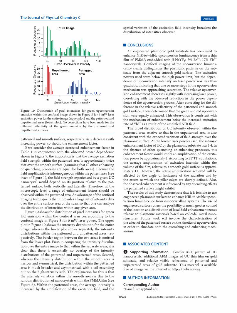
If we consider the average corrected enhancement factor inTable 1 in conjunction with the observed power dependenceshown in Figure 9, the implication is that the average excitationfield strength within the patterned area is approximately twicethat over the smooth surface (assuming that all other enhancingor quenching processes are equal for both areas). Because thefield amplification is inhomogeneous within the pattern area (seeinset of Figure 1), the field strength experienced by a given UCnanocrystal would depend on its position relative to the pat-terned surface, both vertically and laterally. Therefore, at themicroscopic level, a range of enhancement factors should beobserved within the patterned area. An advantage of the confocalimaging technique is that it provides a large set of intensity dataover the entire surface area of the scan, so that one can analyzethe distribution of intensities within any given area.
Figure 10 shows the distribution of pixel intensities for greenUC emission within the confocal scan corresponding to theconfocal image in Figure 8 for 6 mW laser power. The upperplot in Figure 10 shows the intensity distribution for the entireimage, whereas the lower plot shows separately the intensitydistributions within the patterned and unpatterned areas, res-pectively. The border region between the two areas is omittedfrom the lower plot. First, in comparing the intensity distribu-tion over the entire image to that within the separate areas, it isclear that there is essentially no overlap of the intensitydistributions of the patterned and unpatterned areas. Second,whereas the intensity distribution within the smooth area isnarrow and symmetrical, the distribution within the patternedarea is much broader and asymmetrical, with a tail extendingout on the high-intensity side. The explanation for this is thatthe intensity variation within the smooth areas is due to therandom distribution of nanocrystals within the PMMA film (seeFigure 6). Within the patterned areas, the average intensity isincreased by the amplification of the excitation field, and the
spatial variation of the excitation field intensity broadens thedistribution of intensities observed.
’CONCLUSIONS
An engineered plasmonic gold substrate has been used toenhance NIR-to-visible upconversion luminescence from a thinfilm of PMMA embedded with β-NaYF4: 3% Er3+, 17% Yb3+
nanocrystals. Confocal imaging of the upconversion lumines-cence clearly distinguishes the plasmonic patterns on the sub-strate from the adjacent smooth gold surface. The excitationpowers used were below the high-power limit, but the depen-dence of upconversion intensity on laser power was less thanquadratic, indicating that one or more steps in the upconversionmechanism was approaching saturation. The relative upconver-sion enhancement decreases slightly with increasing laser power,correlating with the observed reduction in the power depen-dence of the upconversion process. After correcting for the dif-ference in the relative reflectivity of the patterned and smoothgold surface, it was determined that the green and red upconver-sion were equally enhanced. This observation is consistent withthe mechanism of enhancement being the increased excitationrate of Yb3+ as a result of the amplified NIR field.
The broad distribution of UC intensity observed within thepatterned area, relative to that in the unpatterned area, is alsoconsistent with the expected variation of field strength over theplasmonic surface. At the lowest laser powers used, the intrinsicenhancement factor of UC by the plasmonic substrate was 3.4. Inthe absence of other quenching or enhancing processes, thisenhancement factor would imply an amplification of the excita-tion power by approximately 2. According to FDTD simulations,the average amplification of excitation intensity within thevolume of the film, relative to a smooth gold surface, is approxi-mately 11. However, the actual amplification achieved will beaffected by the angle of incidence of the radiation and bythe extent to which the pillar edges are sharply defined. Also,the observed enhancement is influenced by any quenching effectsthe patterned surface might exhibit.
The results of this study demonstrate that it is feasible to useengineered plasmonic surfaces to enhance NIR-to-visible upcon-version luminescence from nanocrystalline systems. The use ofengineered surfaces offers the possibility of much greater controlof the location and distribution of local-field enhancement zonesrelative to plasmonic materials based on colloidal metal nano-structures. Future work will involve the characterization ofthe effect of the patterned surface on the kinetics of upconversionin order to elucidate both the quenching and enhancing mech-anisms.
’ASSOCIATED CONTENT
bS Supporting Information. Powder XRD pattern of UCnanocrystals, additional AFM images of UC thin film on goldsubstrate, and relative visible reflectance of patterned andunpatterned areas of gold substrate. This material is availablefree of charge via the Internet at http://pubs.acs.org.
’AUTHOR INFORMATION
Corresponding Author*E-mail: [email protected].
Figure 10. Distribution of pixel intensities for green upconversionemission within the confocal image shown in Figure 8 for 6 mW laserexcitation power for the entire image (upper plot) and the patterned andunpatterned areas (lower plot). No corrections have been made for thedifferent reflectivity of the green emission by the patterned andunpatterned surfaces.

19036 dx.doi.org/10.1021/jp206053f |J. Phys. Chem. C 2011, 115, 19028–19036
The Journal of Physical Chemistry C ARTICLE
’ACKNOWLEDGMENT
This material is based upon work supported by the NationalScience Foundation (EPSCoR 0903804 and CHE 0840507) andby the State of SouthDakota. Additional support was provided byResearch Corporation (CC6748) and the National Aeronauticsand Space Administration (Cooperative Agreement Number:NNX10AN34A). The authors acknowledge Lynn Gedvilasof the Electro-optics Characterization group at NREL for makingthe reflectivity measurements. The authors also acknowledgethe Nanofabrication Center at the University of Minnesota forproviding access to the electron beam lithography and thermalevaporation systems.
’REFERENCES
(1) Auzel, F. Chem. Rev. 2004, 104, 139–174.(2) Suyver, J. F.; Aebischer, A.; Biner, D.; Gerner, P.; Grimm, J.;
Heer, S.; Kr€amer, K. W.; Reinhard, C.; G€udel, H. U. Opt. Mater. 2005,27, 1111–1130.(3) Gamelin, D. R.; G€udel, H. U. Transition Metal and Rare Earth
Compounds: Excited States, Transitions, Interactions; Springer: Berlin,2001.(4) Vennerberg, D.; Lin, Z. Sci. Adv. Mater. 2011, 3, 26–40.(5) Wang, F.; Banerjee, D.; Liu, Y.; Chen, X.; Liu, X. Analyst 2010,
135, 1839–1854.(6) van der Ende, B. M.; Aarts, L.; Meijerink, A. Phys. Chem. Chem.
Phys. 2009, 11, 11081–11095.(7) Wang, F.; Liu, X. Chem. Soc. Rev. 2009, 38, 976–989.(8) Heer, S.; Kompe, K.; G€udel, H. U.; Haase, M. Adv. Mater. 2004,
16, 2102–2105.(9) Zhang, P.; Steelant, W.; Kumar, M.; Scholfield, M. J. Am. Chem.
Soc. 2007, 129, 4526–4527.(10) Qian, H. S.; Guo, H. C.; Ho, P. C.-L.; Mahendran, R.; Zhang, Y.
Small 2009, 5, 2285–2290.(11) Downing, E.; Hesselink, L.; Ralston, J.; Macfarlane, R. Science
1996, 273, 1185–1189.(12) Hinklin, T. R.; Rand, S. C.; Laine, R. M. Adv. Mater. 2008,
20, 1270–1273.(13) Liu, X.; Dong, G.; Qiao, Y.; Qiu, J. Appl. Opt. 2008, 47,
6416–6421.(14) Wang, F.; Han, Y.; Lim, C. S.; Lu, Y.; Wang, J.; Xu, J.; Chen, H.;
Zhang, C.; Hong, M.; Liu, X. Nature 2010, 463, 1061–1065.(15) Kim, W. J.; Nyk, M.; Prasad, P. N. Nanotechnology 2009,
20, 185301.(16) Lim, S. F.; Riehn, R.; Ryu, W. S.; Khanarian, N.; Tung, C.-k.;
Tank, D.; Austin, R. H. Nano Lett. 2006, 6, 169–174.(17) Nyk, M.; Kumar, R.; Ohulchanskyy, T. Y.; Bergey, E. J.; Prasad,
P. N. Nano Lett. 2008, 8, 3834–3838.(18) Chen, G.; Ohulchanskyy, T. Y.; Kumar, R.; Ågren, H.; Prasad,
P. N. ACS Nano 2010, 4, 3163–3168.(19) Aebischer, A.; Heer, S.; Biner, D.; Kramer, K.; Haase, M.;
Gudel, H. U. Chem. Phys. Lett. 2005, 407, 124–128.(20) Boyer, J. C.; Vetrone, F.; Cuccia, L. A.; Capobianco, J. A. J. Am.
Chem. Soc. 2006, 128, 7444–7445.(21) Mai, H. X.; Zhang, Y. W.; Si, R.; Yan, Z. G.; Sun, L. D.; You,
L. P.; Yan, C. H. J. Am. Chem. Soc. 2006, 128, 6426–6436.(22) Wang, L.; Li, Y. Nano Lett. 2006, 6, 1645–1649.(23) Wei, Y.; Lu, F.; Zhang, X.; Chen, D. Chem. Mater. 2006,
18, 5733–5737.(24) Yi, G. S.; Chow, G. M. Adv. Funct. Mater. 2006, 16, 2324–9.(25) Mai, H. X.; Zhang, Y. W.; Sun, L. D.; Yan, C. H. J. Phys. Chem. C
2007, 111, 13721–13729.(26) Schafer, H.; Ptacek, P.; Kaempe, K.; Haase, M. Chem. Mater.
2007, 19, 1396–1400.(27) Wang, L.; Li, Y. Chem. Mater. 2007, 19, 727–734.(28) Yi, G. S.; Chow, G. M. Chem. Mater. 2007, 19, 341–343.
(29) Lin, C.; Berry, M. T.; Anderson, R.; Smith, S.; May, P. S. Chem.Mater. 2009, 21, 3406–3413.
(30) Johnson, N. J. J.; Sangeetha, N. M.; Boyer, J.-C.; van Veggel, F.C. J. M. Nanoscale 2010, 2, 771–777.
(31) Bogdan, N.; Vetrone, F.; Ozin, G. A.; Capobianco, J. A. NanoLett. 2011, 11, 835–840.
(32) Suyver, J. F.; Grimm, J.; Kr€amer, K. W.; G€udel, H. U. J. Lumin.2005, 114, 53–59.
(33) Moskovits, M. Rev. Mod. Phys. 1985, 57, 783.(34) Lakowicz, J. R. Anal. Biochem. 2001, 298, 1–24.(35) Bauer, G.; Hassmann, J.; Walter, H.; Haglmueller, J.; Mayer, C.;
Schalkhammer, T. Nanotechnology 2003, 14, 1289–1311.(36) Lakowicz, J. R. Anal. Biochem. 2005, 337, 171–194.(37) Maier, S. A. Plasmonics: Fundamentals and Applications; Spring-
er: New York, 2007.(38) Fort, E.; Gresillon, S. J. Phys. D: Appl. Phys 2008, 41, 013001.(39) Schuller, J. A.; Barnard, E. S.; Cai, W.; Jun, Y. C.; White, J. S.;
Brongersma, M. L. Nat. Mater. 2010, 9, 193–204.(40) Zhu, J.; Zhu, K.; Chen, L. J. Non-Cryst. Solids 2006, 352,
150–154.(41) da Silva, D. M.; Kassab, L. R. P.; L€uthi, S. R.; de Ara�ujo, C. B.;
Gomes, A. S. L.; Bell, M. J. V. Appl. Phys. Lett. 2007, 90, 081913.(42) Kassab, L. R. P.; de Ara�ujo, C. B.; Kobayashi, R. A.; de Almeida
Pinto, R.; da Silva, D. M. J. Appl. Phys. 2007, 102, 103515.(43) Verhagen, E.; Kuipers, L.; Polman, A. Nano Lett. 2007,
7, 334–337.(44) Rai, V. K.;Menezes, L. d. S.; de Ara�ujo, C. B.; Kassab, L. R. P.; da
Silva, D. M.; Kobayashi, R. A. J. Appl. Phys. 2008, 103, 093526.(45) Feng, W.; Sun, L. D.; Yan, C. H. Chem. Commun. 2009,
4393–4395.(46) Kassab, L. R. P.; Bomfim, F. A.; Martinelli, J. R.; Wetter, N. U.;
Neto, J. J.; de Ara�ujo, C. B. Appl. Phys. B: Lasers Opt. 2009, 94, 239–242.(47) Bomfim, F. A.; Martinelli, J. R.; Kassab, L. R. P.; Assumpcao,
T. A. A.; de Ara�ujo, C. B. J. Non-Cryst. Solids 2010, 356, 2598–2601.(48) Schietinger, S.; Aichele, T.; Wang, H.-Q.; Nann, T.; Benson, O.
Nano Lett. 2010, 10, 134–138.(49) Wei, H.-y.; Lin, J.; Feng, Z.-b.; Li, D.-w.; Ma, Y.; Huang, W.-h.
Mater. Sci. Eng., B 2010, 172, 321–326.(50) Zhang, H.; Xu, D.; Huang, Y.; Duan, X. Chem. Commun. 2011,
47, 979–981.(51) Verhagen, E.; Kuipers, L.; Polman, A. Opt. Express 2009, 17,
14586–14598.(52) Paudel, H. P.; B., K.; Baroughi, M. F.; May, S.; Galipeau, D.Opt.
Express 2009, 17, 22179–22189.(53) Paudel, H. P.; Farrokh Baroughi, M.; Bayat, K. J. Opt. Soc. Am. B
2010, 27, 1693–1697.(54) Paudel, H. P.; Bayat, K.; Baroughi, M. F.; May, S.; Galipeau,
D. W. In IEEE PVSC, 35th, Honolulu, HI; IEEE: Piscataway, NJ, 2010;pp 002938�002942.
(55) Song, J. H.; Atay, T.; Shi, S.; Urabe, H.; Nurmikko, A. V. NanoLett. 2005, 5, 1557–1561.
(56) Suyver, J. F.; Aebischer, A.; García-Revilla, S.; Gerner, P.;G€udel, H. U. Phys. Rev. B 2005, 71, 125123.
(57) Suyver, J. F.; Grimm, J.; van Veen, M. K.; Biner, D.; Kr€amer,K. W.; G€udel, H. U. J. Lumin. 2006, 117, 1–12.