emulating the glink chip-set with fpga serial transceivers ... · emulating the glink chip-set with...
TRANSCRIPT
Emulating the GLink Chip-Set with FPGA SerialTransceivers in the ATLAS Level-1 Muon Trigger
Alberto Aloisio, Francesco Cevenini, Raffaele Giordano and Vincenzo Izzo
Abstract—Many High Energy Physics experiments based theirserial links on the Agilent HDMP-1032/34A serializer/deserializerchip-set (or GLink). This success was mainly due to the fact thatthis pair of chips was able to transfer data at ∼ 1 Gb/s with adeterministic latency, fixed after each power up or reset of thelink. Despite this unique timing feature, Agilent discontinued theproduction and no compatible commercial off-the-shelf chip-setsare available. The ATLAS Level-1 Muon trigger includes someserial links based on GLink in order to transfer data from thedetector to the counting room. The transmission side of the linkswill not be upgraded, however a replacement for the receiversin the counting room in case of failures is needed.
In this paper, we present a solution to replace GLink trans-mitters and receivers. Our design is based on the gigabit serialIO (GTP) embedded in a Xilinx Virtex 5 Field ProgrammableGate Array (FPGA). We present the architecture and we discussparameters of the implementation such as latency and resourceoccupation. We compare the GLink chip-set and the GTP-basedemulator in terms of latency, eye diagram and power dissipation.
Index Terms—Serial links, fixed latency, FPGAs.
I. INTRODUCTION
TRIGGER systems of High Energy Physics (HEP) ex-periments need data transfers to be executed with fixed
latency, in order to preserve the timing information. This re-quirement is not necessarily satisfied by Serializer-Deserializer(SerDes) chip-sets. The Gigabit link, or GLink, chip-set [1],produced by Agilent, was able to transfer data at data-rates upto 1 Gb/s with a fixed latency even after a power-cycle or aloss of lock. Serial links of data acquisition systems of HEPexperiments have been often based the GLink chip-set. For in-stance it has been deployed in the Alice [2], ATLAS [3], Babar[4], CDF [5], CMS [6], D0 [7] and Nemo [8] experiments (justto cite some of them). The chip-set became so popular, thatCERN produced a radiation hard serializer compatible withit [9]. Unfortunately, a few years ago Agilent discontinuedthe production of the chip-set and users needing replacementsare looking for alternative solutions. Latest FPGAs includeembedded multi-Gigabit SerDes, which offer a wide variety ofconfigurable features. The benefit from the integration of sucha device in FPGA is obvious in terms of power consumption,size, board layout complexity, cost and re-programmability.The Level-1 Barrel Muon Trigger of the ATLAS experiment
Manuscript received May 23, 2009.A. Aloisio, F. Cevenini and R. Giordano are with INFN Sezione di Napoli
and Università degli Studi di Napoli "Federico II", Dipartimento di ScienzeFisiche, 80126, Napoli, Italy
V. Izzo is with INFN Sezione di Napoli, Dipartimento di Scienze Fisiche,80126, Napoli, Italy
e-mail: [email protected]; [email protected]; [email protected];[email protected].
includes GLink serial links in order to transfer data from thedetector to the counting room. The transmission side of thelinks is on-detector and will unlikely be upgraded, however areplacement for the receivers in the counting room in case offailures is needed. We developed a replacement solution forGLink transmitters and receivers, based on the gigabit serialIO (GTP) embedded in Xilinx Virtex 5 Field ProgrammableGate Array (FPGA). Our solution preserves the fixed-latencyfeature of the original chip-set. In the coming sections wewill introduce the present L1 Barrel Muon Trigger and theGLink chip-set, then we will describe the architecture and theimplementation of our design. Eventually we will present sometest results about our emulator, comparing them also with theGLink chip-set.
II. ATLAS BARREL MUON TRIGGER AND DAQ
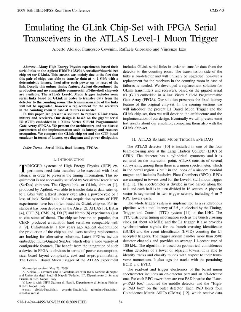
The ATLAS detector [10] is installed in one of the fourbeam-crossing sites at the Large Hadron Collider (LHC) ofCERN. The detector has a cylindrical symmetry and it iscentered on the interaction point. ATLAS consists of severalsubsystems, among them there is a muon spectrometer, whichin the barrel region is built in the loops of a air-core toroidalmagnet and includes Resistive Plate Chambers (RPCs). RPCsare arranged in towers used for the Level-1 (L1) muon trigger(Fig. 1). The spectrometer is divided in two halves along theaxis and each half is in turn divided in 16 sectors. A physicalsector is segmented in two trigger sectors, including 6 or 7RPC towers each.
The whole trigger system is implemented as a synchronouspipeline, with a total latency of 2.5 µs, clocked by the Timing,Trigger and Control (TTC) system [11] of the LHC. TheTTC distributes timing information such as the bunch crossingclock (at about 40 MHz) and the L1 trigger. It also providessynchronization signals for the bunch crossing identificator(BCID) and the event identificator (EVID) counting the L1accepted triggers. The trigger system handles more than 350kdetector channels and provides an average L1-accept rate of100 kHz. The algorithm is based on geometrical coincidenceswithin detectors of a tower or adjacent towers. It is able toidentify tracks and classify muons with respect to their trans-verse momentum. It also tags the tracks with the pertainingBCID and EVID.
The read-out and trigger electronics of the barrel muonspectrometer includes an on-detector part and an off-detectorone. For each RPC tower there are two PAD boards: the “Low-pT PAD box” mounted the middle detector and the “High-pT PAD box” on the outer detector. Each PAD hosts fourCoincidence Matrix ASICs (CMAs) [12], which receive data
2009 16th IEEE-NPSS Real Time Conference CMSP-3
978-1-4244-4455-7/09/$25.00 ©2009 IEEE 84
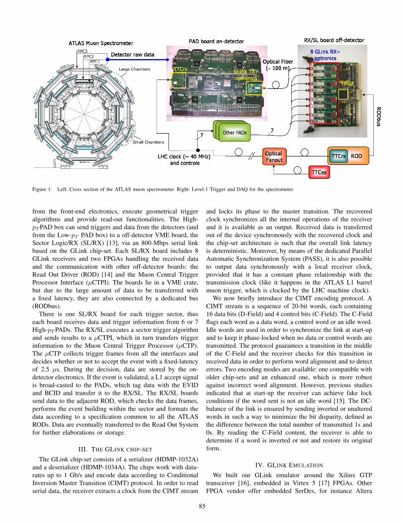
Figure 1. Left: Cross section of the ATLAS muon spectrometer. Right: Level-1 Trigger and DAQ for the spectrometer.
from the front-end electronics, execute geometrical triggeralgorithms and provide read-out functionalities. The High-pT PAD box can send triggers and data from the detectors (andfrom the Low-pT PAD box) to a off-detector VME board, theSector Logic/RX (SL/RX) [13], via an 800-Mbps serial linkbased on the GLink chip-set. Each SL/RX board includes 8GLink receivers and two FPGAs handling the received dataand the communication with other off-detector boards: theRead Out Driver (ROD) [14] and the Muon Central TriggerProcessor Interface (µCTPI). The boards lie in a VME crate,but due to the large amount of data to be transferred witha fixed latency, they are also connected by a dedicated bus(RODbus).
There is one SL/RX board for each trigger sector, thuseach board receives data and trigger information from 6 or 7High-pT PADs. The RX/SL executes a sector trigger algorithmand sends results to a µCTPI, which in turn transfers triggerinformation to the Muon Central Trigger Processor (µCTP).The µCTP collects trigger frames from all the interfaces anddecides whether or not to accept the event with a fixed-latencyof 2.5 µs. During the decision, data are stored by the on-detector electronics. If the event is validated, a L1 accept signalis broad-casted to the PADs, which tag data with the EVIDand BCID and transfer it to the RX/SL. The RX/SL boardssend data to the adjacent ROD, which checks the data frames,performs the event building within the sector and formats thedata according to a specification common to all the ATLASRODs. Data are eventually transferred to the Read Out Systemfor further elaborations or storage.
III. THE GLINK CHIP-SET
The GLink chip-set consists of a serializer (HDMP-1032A)and a deserializer (HDMP-1034A). The chips work with data-rates up to 1 Gb/s and encode data according to ConditionalInversion Master Transition (CIMT) protocol. In order to readserial data, the receiver extracts a clock from the CIMT stream
and locks its phase to the master transition. The recoveredclock synchronizes all the internal operations of the receiverand it is available as an output. Received data is transferredout of the device synchronously with the recovered clock andthe chip-set architecture is such that the overall link latencyis deterministic. Moreover, by means of the dedicated ParallelAutomatic Synchronization System (PASS), it is also possibleto output data synchronously with a local receiver clock,provided that it has a constant phase relationship with thetransmission clock (like it happens in the ATLAS L1 barrelmuon trigger, which is clocked by the LHC machine clock).
We now briefly introduce the CIMT encoding protocol. ACIMT stream is a sequence of 20-bit words, each containing16 data bits (D-Field) and 4 control bits (C-Field). The C-Fieldflags each word as a data word, a control word or an idle word.Idle words are used in order to synchronize the link at start-upand to keep it phase-locked when no data or control words aretransmitted. The protocol guarantees a transition in the middleof the C-Field and the receiver checks for this transition inreceived data in order to perform word alignment and to detecterrors. Two encoding modes are available: one compatible witholder chip-sets and an enhanced one, which is more robustagainst incorrect word alignment. However, previous studiesindicated that at start-up the receiver can achieve fake lockconditions if the word sent is not an idle word [15]. The DC-balance of the link is ensured by sending inverted or unalteredwords in such a way to minimize the bit disparity, defined asthe difference between the total number of transmitted 1s and0s. By reading the C-Field content, the receiver is able todetermine if a word is inverted or not and restore its originalform.
IV. GLINK EMULATION
We built our GLink emulator around the Xilinx GTPtransceiver [16], embedded in Virtex 5 [17] FPGAs. OtherFPGA vendor offer embedded SerDes, for instance Altera
85
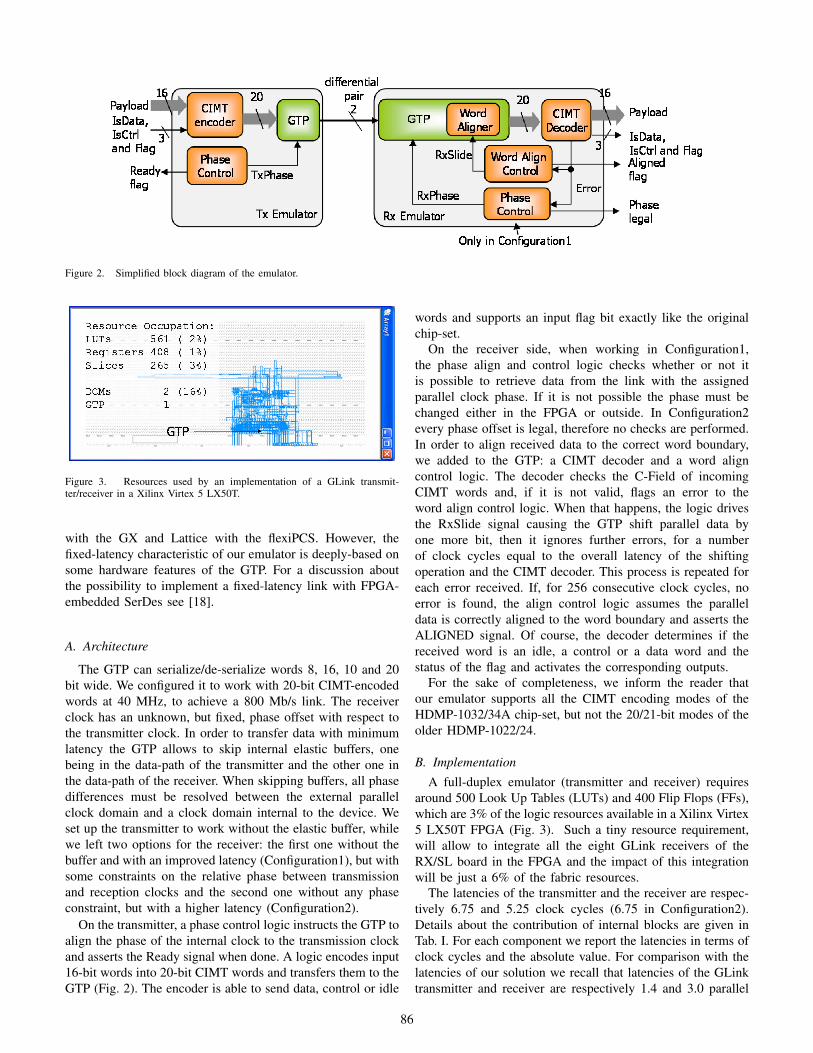
Figure 2. Simplified block diagram of the emulator.
Figure 3. Resources used by an implementation of a GLink transmit-ter/receiver in a Xilinx Virtex 5 LX50T.
with the GX and Lattice with the flexiPCS. However, thefixed-latency characteristic of our emulator is deeply-based onsome hardware features of the GTP. For a discussion aboutthe possibility to implement a fixed-latency link with FPGA-embedded SerDes see [18].
A. Architecture
The GTP can serialize/de-serialize words 8, 16, 10 and 20bit wide. We configured it to work with 20-bit CIMT-encodedwords at 40 MHz, to achieve a 800 Mb/s link. The receiverclock has an unknown, but fixed, phase offset with respect tothe transmitter clock. In order to transfer data with minimumlatency the GTP allows to skip internal elastic buffers, onebeing in the data-path of the transmitter and the other one inthe data-path of the receiver. When skipping buffers, all phasedifferences must be resolved between the external parallelclock domain and a clock domain internal to the device. Weset up the transmitter to work without the elastic buffer, whilewe left two options for the receiver: the first one without thebuffer and with an improved latency (Configuration1), but withsome constraints on the relative phase between transmissionand reception clocks and the second one without any phaseconstraint, but with a higher latency (Configuration2).
On the transmitter, a phase control logic instructs the GTP toalign the phase of the internal clock to the transmission clockand asserts the Ready signal when done. A logic encodes input16-bit words into 20-bit CIMT words and transfers them to theGTP (Fig. 2). The encoder is able to send data, control or idle
words and supports an input flag bit exactly like the originalchip-set.
On the receiver side, when working in Configuration1,the phase align and control logic checks whether or not itis possible to retrieve data from the link with the assignedparallel clock phase. If it is not possible the phase must bechanged either in the FPGA or outside. In Configuration2every phase offset is legal, therefore no checks are performed.In order to align received data to the correct word boundary,we added to the GTP: a CIMT decoder and a word aligncontrol logic. The decoder checks the C-Field of incomingCIMT words and, if it is not valid, flags an error to theword align control logic. When that happens, the logic drivesthe RxSlide signal causing the GTP shift parallel data byone more bit, then it ignores further errors, for a numberof clock cycles equal to the overall latency of the shiftingoperation and the CIMT decoder. This process is repeated foreach error received. If, for 256 consecutive clock cycles, noerror is found, the align control logic assumes the paralleldata is correctly aligned to the word boundary and asserts theALIGNED signal. Of course, the decoder determines if thereceived word is an idle, a control or a data word and thestatus of the flag and activates the corresponding outputs.
For the sake of completeness, we inform the reader thatour emulator supports all the CIMT encoding modes of theHDMP-1032/34A chip-set, but not the 20/21-bit modes of theolder HDMP-1022/24.
B. ImplementationA full-duplex emulator (transmitter and receiver) requires
around 500 Look Up Tables (LUTs) and 400 Flip Flops (FFs),which are 3% of the logic resources available in a Xilinx Virtex5 LX50T FPGA (Fig. 3). Such a tiny resource requirement,will allow to integrate all the eight GLink receivers of theRX/SL board in the FPGA and the impact of this integrationwill be just a 6% of the fabric resources.
The latencies of the transmitter and the receiver are respec-tively 6.75 and 5.25 clock cycles (6.75 in Configuration2).Details about the contribution of internal blocks are given inTab. I. For each component we report the latencies in terms ofclock cycles and the absolute value. For comparison with thelatencies of our solution we recall that latencies of the GLinktransmitter and receiver are respectively 1.4 and 3.0 parallel
86
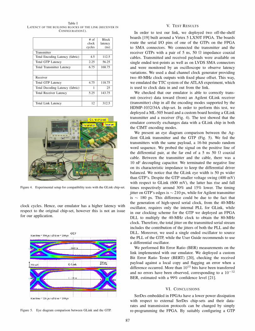
Table ILATENCY OF THE BUILDING BLOCKS OF THE LINK (RECEIVER IN
CONFIGURATION1).
# ofclock
cycles
Blocklatency
(ns)
TransmitterTotal Encoding Latency (fabric) 4.5 112.5
Total GTP Latency 2.25 56.25
Total Transmitter Latency 6.75 168.75
Receiver
Total GTP Latency 4.75 118.75
Total Decoding Latency (fabric) 1 25
Total Receiver Latency 5.25 143.75
Total Link Latency 12 312.5
Figure 4. Experimental setup for compatibility tests with the GLink chip-set.
clock cycles. Hence, our emulator has a higher latency withrespect to the original chip-set, however this is not an issuefor our application.
Figure 5. Eye diagram comparison between GLink and the GTP.
V. TEST RESULTS
In order to test our link, we deployed two off-the-shelfboards [19] built around a Virtex 5 LX50T FPGA. The boardsroute the serial I/O pins of one of the GTPs on the FPGAto SMA connectors. We connected the transmitter and thereceiver GTPs with a pair of 5 ns, 50 Ω impedance coaxialcables. Transmitted and received payloads were available onsingle ended test-points as well as on LVDS SMA connectorsand were monitored by an oscilloscope to observe latencyvariations. We used a dual channel clock generator providingtwo 40-MHz clock outputs with fixed phase offset. This way,we emulated the TTC system of the ATLAS experiment, whichis used to clock data in and out from the link.
We checked that our emulator is able to correctly trans-mit (receive) data toward (from) an Agilent GLink receiver(transmitter) chip in all the encoding modes supported by theHDMP-1032/34A chip-set. In order to perform this test, wedeployed a ML-505 board and a custom board hosting a GLinktransmitter and a receiver (Fig. 4). The test showed that theemulator correctly exchanges data with a GLink chip in boththe CIMT encoding modes.
We present an eye diagram comparison between the Ag-ilent GLink transmitter and the GTP (Fig. 5). We fed thetransmitters with the same payload, a 16-bit pseudo randomword sequence. We probed the signal on the positive line ofthe differential pair, at the far end of a 5 ns 50 Ω coaxialcable. Between the transmitter and the cable, there was a10 nF decoupling capacitor. We terminated the negative lineon its characteristic impedance to keep the differential driverbalanced. We notice that the GLink eye width is 50 ps widerthan GTP’s. Despite the GTP smaller voltage swing (400 mV)with respect to GLink (600 mV), the latter has rise and falltimes respectively around 30% and 15% lower. The timingjitter on GTP’s edges is ∼ 210 ps, while for Agilent transmitteris ∼ 180 ps. This difference could be due to the fact thatthe generation of high-speed serial clock, from the 40-MHzoscillator, requires only the internal PLL for GLink, whilein our clocking scheme for the GTP we deployed an FPGADLL to multiply the 40-MHz clock to obtain the 80-MHzclock. Therefore, the total jitter on the transmitted serial streamincludes the contribution of the jitters of both the PLL and theDLL. Moreover, we used a single ended oscillator to sourcethe PLL of the GTP, while the User Guide recommends to usea differential oscillator.
We performed Bit Error Ratio (BER) measurements on thelink implemented with our emulator. We deployed a customBit Error Ratio Tester (BERT) [20], checking the receivedpayload against a local copy and flagging an error when adifference occurred. More than 1013 bits have been transferredand no errors have been observed, corresponding to a 10− 12
BER, estimated with a 99% confidence level [21].
VI. CONCLUSIONS
SerDes embedded in FPGAs have a lower power dissipationwith respect to external SerDes chip-sets and their data-rates and transmission protocols can be changed by simplyre-programming the FPGA. By suitably configuring a GTP
87
transceiver and adding few logic resources from the FPGAfabric (~ 3% of the total), we have been able to achieve acomplete replacement for the GLink chip-set. Our emulatortransfers data with a fixed latency, which was a crucialfeature of the original chip-set. We experimentally verified thecompatibility of our emulator with GLink both in transmissionand reception. The emulator has a tiny footprint in terms oflogic resources and, in a future upgrade of the RX/SL, it willallow us to integrate all the GLink receivers on the boardin a single FPGA, still leaving most of the device resourcesfree to for trigger and readout tasks. Hence, the layout ofthe upgraded board would be simplified with respect to thepresent. A GLink receiver dissipates ~ 800 mW (typical @1Gb/s) while each GTP pair (transmitter and receiver) dissipates~ 300 mW (typical @3 Gb/s), hence also the overall powerdissipation of the board will be lowered in the upgrade.
ACKNOWLEDGMENT
The authors are thankful to Giovanni Guasti and FrancescoContu from Xilinx Italy for their support and help in con-figuring the GTP transceiver. This work is partly supportedas a PRIN project by the Italian Ministero dell’Istruzione,Università e Ricerca Scientifica.
REFERENCES
[1] (2001). Agilent HDMP 1032-1034 Transmitter-Receiver Chip-setDatasheet, Agilent [On-line]. Available: http://www.physics.ohio-state.edu/~cms/cfeb/datasheets/hdmp1032.pdf
[2] Kluge, A. for the ALICE SPD collaboration, “The Read-Out sys-tem of the ALICE pixel detector”, Proceedings of the InternationalWorkshop on Semiconductor Pixel Detectors for Particles and X-Rays(PIXEL2002)
[3] J. Garvey et al., “The ATLAS Level-1 Calorimeter Trigger Architecture”,IEEE Transactions on Nucl. Sci., Vol. 51, no. 3, June 2004
[4] P. Sanders, “The BaBar trigger, readout and event gathering system”,IEEE Trans. on Nucl. Sci., Vol. 45, Issue 4, Part 1, August 1998 pp.1894-1897
[5] W. Ashmanskas et al., “Silicon vertex tracker: a fast precise trackingtrigger for CDF”, Nuclear Instruments and Methods in Physics ResearchSection A, Vol. 447, Issues 1-2, June 2000, pp. 218-222
[6] B. Lofstedt On behalf of the CMS ECAL Collaboration, “The digitalreadout system for the CMS electromagnetic calorimeter”, Volume 453,Issues 1-2, 11 October 2000, pp. 433-439
[7] James T. Linnemann, “The D0 Level 2 Trigger” International journal ofmodern physics. C, Physics and computers, vol. 16, issue 1, 2001, p.1166
[8] F. Ameli, “The Data Acquisition and Transport Design for NEMO Phase1”, IEEE Trans. on Nucl. Sci., Vol. 55, Issue 1, Part 1, Feb. 2008 pp.233-240
[9] P. Moreira, T. Toifl, A. Kluge, G. Cervelli, F. Faccio, A. Marchioro, J.Christiansen, “GLink and gigabit Ethernet compliant serializer for LHCdata transmission”, Nuclear Science Symposium Conference Record,15-20 Oct. 2000, Vol. 2 , pp. 9/6 - 9/9
[10] ATLAS Collaboration, ATLAS Detector and Physics Performance- Technical Design Report - Volume I, May 1999 [On-line]. Available: http://atlas.web.cern.ch/Atlas/GROUPS/PHYSICS/TDR/physics_tdr/printout/Volume_I.pdf
[11] B.G. Taylor for the RD12 Project Collaboration, TTC Distribution forLHC Detectors, IEEE Trans. on Nucl. Sci., Vol. 45, No. 3, June 1998,pp. 821-828.
[12] F. Pastore, E. Petrolo, R. Vari, S. Veneziano, “Performances of theCoincidence Matrix ASIC of the ATLAS Barrel Level-1 Muon Trigger”,Proceedings of the 11th Workshop on Electronics for LHC Experiments,Heidelberg, Germany, 12-16 Sept 2005.
[13] G.Chiodi, E.Gennari, E.Petrolo, F.Pastore, A.Salamon, R.Varia,S.Veneziano, “The ATLAS barrel level-1 Muon Trigger Sector-Logic/RX off-detector trigger and acquisition board”, Topical Workshopon Electronics for Particle Physics, Prague, Czech Republic, 03 - 07Sep 2007, pp.232-237
[14] A. Aloisio et al., “The Read-Out Driver for the RPC of the ATLASMuon Spectrometer”, IEEE Trans. Nuclear Science, Vol. 55, no.1, part1, 2008, pp. 265-271
[15] A. Aloisio, F. Cevenini, V. Izzo, “Do’s and Don’ts With the Agilent’sGLink Chipset “, IEEE Trans. on Nucl. Sci., vol. 53, no. 3, June 2006
[16] (2008). Virtex-5 FPGA RocketIO GTP Transceiver UserGuide - UG196 (v1.7), Xilinx [On-line]. Available:http://www.xilinx.com/support/documentation/user_guides/ug196.pdf
[17] (2008). Virtex-5 FPGA User Guide -UG190 (v4.3), Xilinx [On-line]. Available:http://www.xilinx.com/support/documentation/user_guides/ug190.pdf
[18] A. Aloisio, F. Cevenini, R. Giordano, V. Izzo, “High-speed, fixed-latencyserial links with FPGAs”, Nuclear Science Symposium ConferenceRecord, 2008, Dresden, Germany, pp. 2137-2142
[19] (2008). ML505/ML506/ML507 Evaluation Platform UserGuide - UG347 (v3.0.1), Xilinx [On-line]. Available:http://www.xilinx.com/support/documentation/boards_and_kits/ug347.pdf
[20] A. Aloisio, F. Cevenini, R. Cicalese, R. Giordano, V. Izzo, “Beyond320 Mbyte/s With 2eSST and Bus Invert Coding on VME64x”, IEEETransactions on Nuclear Science, Volume 55, Issue 1, Feb. 2008, pp.203-208
[21] (2007). Statistical Confidence Levels for Estimating ErrorProbability, Maxim [On-line]. Available: http://pdfserv.maxim-ic.com/en/an/AN1095.pdf
88