elektronikkurs 2011 some topics in opto-electronics · elektronikkurs 2011 some topics in...
TRANSCRIPT

Elektronikkurs 2011 Some Topics in Opto-Electronics
Overview of radiation detectors
Rules of Thumb from Phil Hobbes: „Building Electro-optical Systems”
Photodiodes
Principles
pn- junction
pn photodiode
pin photodiode
Measurements with PIN diode module
Application: Laser energy measurement
Amplification of photocurrent
Amplifying principles
Resistance
Capacitance
Transimpedance
Transadmittance
Schematics of proven detector amplification circuits
Simple Transimpedance Amplifier
Parasitic-C Charge Amplifier
Resonant Amplifier
Application Notes
Oriel: Detectors Technical Diskussions
Optoelectronic Components German Text from Böhmer, “Elemente der angewandten Elektronik”

Elektronikkurs 2011 Some Topics in Opto-Electronics
LED
Fototransistor
Optokoppler
Lichtschranke
Faseroptik
LCD

Detectors based onphotoeffect (Quantum or
Photon Detectors)
internal photoeffect(innerer Photoeffekt)
Free carriers interaction(Zusammenwirken vonfreien Ladungsträgern)
external or photoemissive photoeffect(äusserer Photoeffekt)
Localized interactionsExcitation of additionalcarriers
(Erzeugung vonzusätzlichen
Ladungsträgern)
Photocathodes(Photokathoden)
Gain mechanism(Vervielfacher)
Photoconductivity(photoleitender
Effekt)
photovoltaic effect
Avalanchephotodiode
Photon drag effect
Hot electronbolometer
Phosphor
Photofilm
Photomultiplier PM
Gas avalanche -proportional chamber
Electron multiplier
Multi-channel plateMPC
Detectors based onthermal effects
Pneumatic effect
Golay cellPhotoacoustic cell
Pyroelectric effect Thermoelectric effectBolometer
ThermopileThermocouple(Thermoelement)
Common Photodetectors
Elektronikkurs LPC 2009


RULES OF THUMB
Solar constant ( just above theatmosphere)
1.36 kW/m2, 20.00 MW/(m2/sr) (sunat zenith)
Solar absolute bolometric magnitudeMbol
4:75
Minimum luminance for easy reading 5 lm/m2 (lux)
Bright room lights 400 lx
Bright desk lamp for close work 7000 lx
Peak luminous e½ciency of light-adapted eye
683 lm/W at 550 nm
FWHM of light-adapted eye 510 to 610 nm
Zenith sunlight at ground level 100,000 lx, 1 kW/m2, 15 MW/(m2/sr)
Brightest stars mv 0 2.54 mlx above atmosphere, 2.0 mlx atground
Faintest naked-eye star mv 6: 1 10ÿ8 lx at top of atmosphere
Black body radiation 56.7 kW/m2 at 1000 K
Earth's magnetic ®eld B 0.3 to 0.6 G
Airy disk radius of circular aperture ofradius a
0.61l=a rad ag l
EÂ tendue of Gaussian beam pl=42Waist radius of Gaussian beam w l=p NA)
Airy disk diameter in the visible aA fa 0:5/NA (a in mm)
Defocus tolerance jDZj < 0:5l/NA2
Peak e½ciency of an optical systemand photodiode
0.4 to 0.8, depending on coatings
Solid angle of uniform cone WA pNA2 4= fa2 for NA < 0:3
Image ¯ux density at f =8(NA 0:063) with distant object
1% of object ¯ux density (Lambertiansource)
Strehl ratio with rms wavefront error E
wavesS A expÿE2=2
Di¨raction limit l=4 rms wavefront error! 0:8 Strehlratio
Hyperfocal distance of lens of diameterD
D2=l
Aberration scaling with NA and ®eldangle
SphericalzNA3, comazNA2 y,astigmatism and ®eld curvaturezNAy2, distortionz y3
Things invariant under magni®cation Radiance, n2A W, resolvable spots,phase shifts, total power
EÂ tendue of optical ®ber (roughly) n2A WA 3 10ÿ6 cm2 sr (SM),10ÿ3 cm2 sr (step index MM)
Responsivity of photodiode h 1 i l=1:240 mm A/W
1-dB increase 26% power, 12% voltage

Additional noise producing 1-dB SNRreduction
5.87 dB below noise ¯oor
Shot noise limit iphotoRL > 2kT=e (50 mV at 300 K)
Shot Noise Rule Of One 1s shift with 1 photon/s in 1 Hzcoherently added
Shot noise of 1 mA 17.90 pA/Hzp
Resistor with Johnson noise of1 nV/
Hzp
at 300 K60.4 W
Resistor with Johnson noise current of1 pA/
Hzp
at 300 K16.56 kW
Noise power with matched source(NF 0 dB for pure Johnson noise)
PJdBm ÿ173:8NF
10 logT
300 10 log BW
Quantization noise 1=12p
ADU
Sine-wave power (50 W) PdBm 4 20 log10Vpp
Transconductance of bipolar transistor gm eiC=kT iC=25:7 mV at 300 K
Sheet resistance of 0.5-oz copper(0.017 mm)
1.0 mW=a at 25C
Inductance of 1-in. component lead A20 nH
Capacitance of a 1-mm square pad ona four-layer card
0.2 pF (ground adjacent), 0.08 pF(ground opposite)
Low-frequency capacitance of RG-58cable
100 pF/m

A) Photodiodes
Aspects of Photodiodes:Principles SensitivityLaserpulse Monitoring
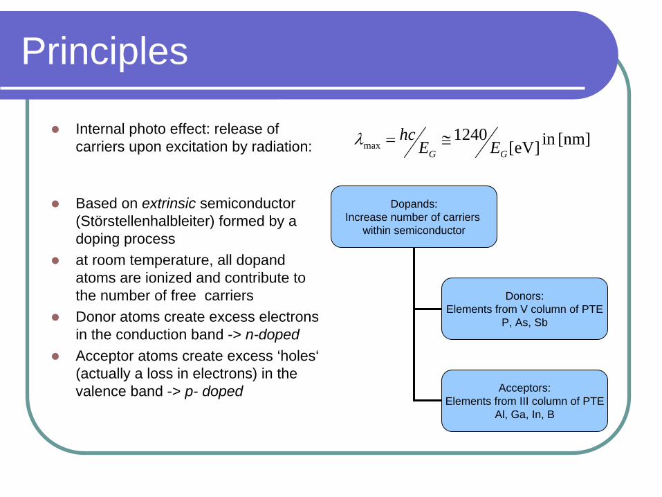
Principles
Internal photo effect: release of carriers upon excitation by radiation:
Based on extrinsic semiconductor (Störstellenhalbleiter) formed by a doping processat room temperature, all dopandatoms are ionized and contribute to the number of free carriersDonor atoms create excess electrons in the conduction band -> n-dopedAcceptor atoms create excess ‘holes‘ (actually a loss in electrons) in the valence band -> p- doped
[nm]in ]eV[1240
maxGG EE
hc ≅=λ
Dopands:Increase number of carriers
within semiconductor
Donors:Elements from V column of PTE
P, As, Sb
Acceptors:Elements from III column of PTE
Al, Ga, In, B

Common Semiconductor Material
Silicon (Si), IV column of PTE:most common material due to its sensitivity over a broad range of technical relevant frequencies –useful from 200nm to 1100nm without special surface treatment; fabrication process very mature;More specialized photodiodes are made of compound semiconductor:
GaAs:fast photodiodesInSb: IR sensitive, fastGaP: solar blind, UV sensitivePbSe:IR sensitive
Compound semiconductor are also used as photocathodes (-> external photoeffect)

pn junction
2 types of current can be distinguished:Diffusion current: due to majority carriers (electrons in n-doped and holes in p-doped material), driving force are fields due to concentration difference across junctionDrift current: due to minority carriers (holes in n-doped and electrons in p-doped semiconductor) which are created by energetic excitation (temperature, radiation)Currents are balanced without external circuitryFermi level adjust and result in a barrier -> built-in voltage

Internal photo effect in pn junctions
Absorption of radiation within the depletion region produces electron-hole pairs. These carriers drift under the force of the internal electric field and hence increase the drift current – but moving carriers also induce (D: influenzieren) a current in the attached external circuitryPhoton energy above the band gap energy is lost as heat within the semiconductor. Responsivity (Empfindlichkeit) = detector output / radiation input ( [A/W] ), usually wavelength dependent; Photon or quantum detectors show a decrease in responsivity towards shorter wavelength compared to thermal detectorsQuantum Efficiency (Quantenausbeute)= number of basic signal elements / number of incidents photons ( [%] )

pn photodiode
Best for (s)low signalHighest homogenaity across sensitive area
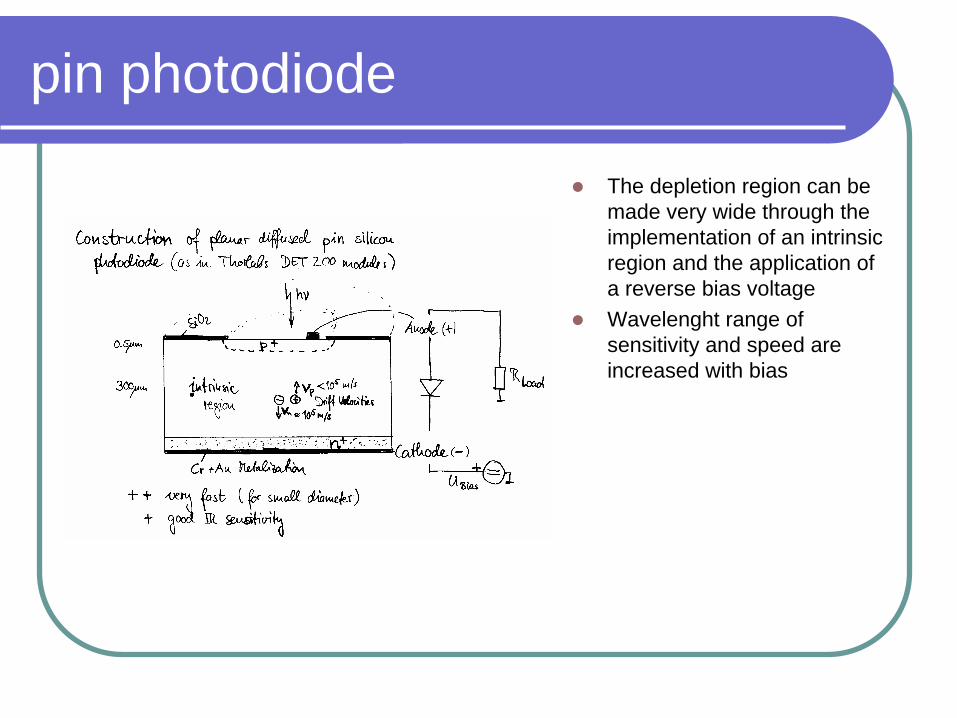
pin photodiode
The depletion region can be made very wide through the implementation of an intrinsic region and the application of a reverse bias voltageWavelenght range of sensitivity and speed are increased with bias

Load Diagram
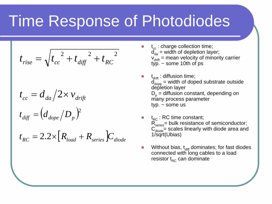
Time Response of Photodiodes
222RCdiffccrise tttt ++=
tcc : charge collection time;dda = width of depletion layer;vdrift = mean velocity of minority carrier typ. ~ some 10th of ps
tdrift : diffusion time;ddope = width of doped substrate outside depletion layerDp = diffusion constant, depending on many process parametertyp. ~ some us
tRC : RC time constant;Rseries= bulk resistance of semiconductor;Cdiode= scales linearly with diode area and 1/sqrt(Ubias)
Without bias, tdiff dominates; for fast diodes connected with long cables to a load resistor tRC can dominate
driftdacc vdt ×= 2
( )2pdopediff Ddt =
[ ] diodeseriesloadRC CRRt +×= 2.2

Attenuation length in Silicon Photodiode
Diode: AXUV-100, NIST
special VUV diode as example
from R. Stuik, Nuclear Instruments and Methods in Physics research A 489 (2002), p. 370ff)
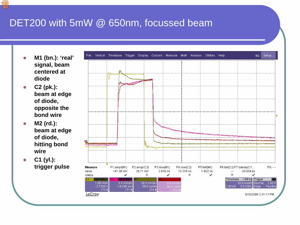
DET200 with 5mW @ 650nm, focussed beam
M1 (bn.): ‘real’ signal, beam centered at diodeC2 (pk.): beam at edge of diode, opposite the bond wireM2 (rd.): beam at edge of diode, hitting bond wireC1 (yl.): trigger pulse

Difference between PIN and PN diode @ focussed 2mW, 650nm short (10ns) pulse
C2 (rd.): DET210 (PIN diode) with bias appliedC3 (bl.): S1336-5BK (PN diode) at 50 ohm load resistorC1 (yl.): trigger pulse

Nd-YAG pulse measured with Thorlabs DET-210 (F11)

Laser Energy Measurements with Photodiodes - ROT
slight advantage in measuring total area of voltage-time across load resistor (correspondes to integrated charge) over measuring peak voltageno difference in saturation level using biased PIN or biased PN diodes – but total charge needs to be measured1% uncertainty for 8ns@532nm from 0.3nJ to 50nJ, for higher fluence clearly saturation! (R. Vest, App.Opt. 42, p.5054)up to 120mW peak power at pulse length up to 10us no sign of saturation with biased PN diode (R. Stuik, NIMPhys.Rsrc. A489, p. 370)4% uncertainty for 10ns@157nm below 11nJ, for higher fluence saturation (M. Richter Appl.Opt. 41, p.7167)Typical Si diode saturates above 3mA photon current with cw radiation

B) Amplification of Photocurrent
Principles Example: Laserpulse MonitoringSchematics of typical circuits

Principles - Resistance
most simple circuitDimension resistance such that-> „I photo * R > 200mV“; thenshot noise will be the dominatingnoise sourceS/N (Signal zu Rausch Verhältnis) is inversely proportional to resistanceBandwidth dictated by parsiticcapacitances of detector and connecting cableExample: Thorlabs Module DET210; New Focus 162X Series
)(*)( tiRtu photo=
)(21 ker)&3 StecKabelDiodedB CCRf +=− π

Principles - Capacitance
most useful for very short, large current pulses -> chargemeasurementsIntegrating time constant givenby parasitic componentsS/N is inversely proportional to capacitanceExample: Home-buildt devices; Ortec 113
∫= dttiCtu photo )(*1)(
paraStecKabelDiode RCC )( ker)&+=τ
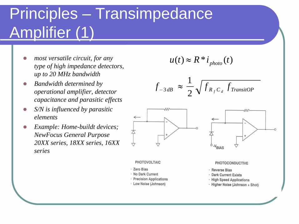
Principles – Transimpedance Amplifier (1)
most versatile circuit, for anytype of high impedance detectors, up to 20 MHz bandwidthBandwidth determined byoperational amplifier, detectorcapacitance and parasitic effectsS/N is influenced by parasiticelementsExample: Home-buildt devices; NewFocus General Purpose20XX series, 18XX series, 16XX series
)(*)( tiRtu photo≈
TransitOPCRdB fffdf2
13 ≈−
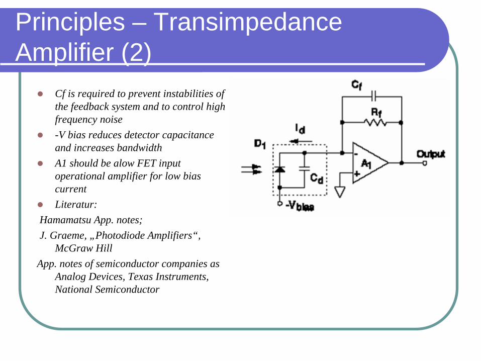
Principles – Transimpedance Amplifier (2)
Cf is required to prevent instabilities of the feedback system and to control high frequency noise-V bias reduces detector capacitanceand increases bandwidthA1 should be alow FET inputoperational amplifier for low biascurrentLiteratur:
Hamamatsu App. notes;J. Graeme, „Photodiode Amplifiers“,
McGraw HillApp. notes of semiconductor companies as
Analog Devices, Texas Instruments, National Semiconductor

Principles – Transadmittance Amplifier (Charge Amplifier)
Fast versions are used in high energyphysics facilities in very large numbersBandwidth is not a commonspecification but rise time and repetitionrateS/N is inversly proportional to CR1 decays output signal in a controlledfashion -> ‚resets‘ the charge amplifierExample: CAEN A422, Amptek A250
∫≈ dttiCtu photo )(*1)(


5
5
4
4
3
3
2
2
1
1
D D
C C
B B
A A
+VCC
-VCC
+VCC
-VCC
Title
Size Document Number Rev
Date: Sheet of
<Doc> <RevCode>
q_amp
A
1 1Friday, March 23, 2001
Title
Size Document Number Rev
Date: Sheet of
<Doc> <RevCode>
q_amp
A
1 1Friday, March 23, 2001
Title
Size Document Number Rev
Date: Sheet of
<Doc> <RevCode>
q_amp
A
1 1Friday, March 23, 2001
Diesen Teil auf Unterseitebestuecken
Multilayer(GRM230Y5V106Z10murata)
Schneller Pulsverstärker mit AC-Kopplung
U= (1/C) * delta I * delta t( Eine zum Strompuls proportionale Spannung über dem Kondensator C10 wird verstärkt )
fGBW = 35MHz, G=5 -> Bandbreite= 7MHz
DC-Gain = 1 (Wegen Kondensatoren C7-C9)
AC-Gain = 1+(1500/390)=4.85
Kondensa
tor um S
trom in
Ladung
umzuset
zen, n
ahe am
Eingan
gplat
zieren.
Bottom,
1M leich
tau
swec
hsel
bar
Stützkondensatorennahe am IC platzieren
Stützkondensatorennahe am IC platzieren
Schematopologie nachbilden..
Diesen TeilaufUnterseitebestuecken
R4 & R5 möglichst kurzer Weg zum IC
GND gut mit Gehäuse kontaktieren
Blaue Schrift sind Layout Hinweise
R4 100R4 100
R5 47R5 47
R6 1.5kR6 1.5kR7
390
R7
390
C12.2u / 25V / TantalC12.2u / 25V / Tantal
C22.2u / 25V / TantalC22.2u / 25V / Tantal
C32.2u / 25V / TantalC32.2u / 25V / Tantal
C42.2u / 25V / TantalC42.2u / 25V / Tantal
L1JOKE / BLM21A102SL1JOKE / BLM21A102S
L2JOKE / BLM21A102SL2JOKE / BLM21A102S
J1+15VJ1+15V
1
J2GNDJ2GND
1
J3-15VJ3-15V
1
J4
Out
J4
Out
1
C510nC510n
C610nC610n
J5
In
J5
In
1
C7
10u / 10V
C7
10u / 10V
C8
10u / 10V
C8
10u / 10V
C9
10n / 10V
C9
10n / 10V
+
-
U1OPA671+
-
U1OPA6713
26
7 54 8 1
R81MR81M
C10
4.7p / C0G
C10
4.7p / C0G
risetime100ns.bmp
H:\Projekte_laufende\NIR_CALIBRATION\

5
5
4
4
3
3
2
2
1
1
D D
C C
B B
A A
-5V
-15VB
+5V
-15VB
-15V-5V
+15V+5V
+15VB
Title
Size Document Number Rev
Date: Sheet of
pda2_94.sch <RevCode>
Photodiode Preamp 40MHz ac coupled
A
1 1Thursday, May 27, 2004
Title
Size Document Number Rev
Date: Sheet of
pda2_94.sch <RevCode>
Photodiode Preamp 40MHz ac coupled
A
1 1Thursday, May 27, 2004
Title
Size Document Number Rev
Date: Sheet of
pda2_94.sch <RevCode>
Photodiode Preamp 40MHz ac coupled
A
1 1Thursday, May 27, 2004
K
ACase
Signal Transformer, Winding Ratio 1:2,Impedance Transformation of 1:4
T1
TTWB1040
T1
TTWB1040
1 6
5
3 4
2
+
C10
2.2u
+
C10
2.2u
C4DummyC4DummyQ1
S3883Q1S3883
1
2
3
-
+
U1
CLC426A
-
+
U1
CLC426A
3
4
62
7 85
R3200R3200
1
2
R6
47
R6
47
JP1Pos-DCJP1Pos-DC
1 2 3 4
C968nC968n
JP3Neg DC
JP3Neg DC
1 2 3 4
C2
470p
C2
470p
R9
10k
R9
10k
1
2
+
C7
2.2u
+
C7
2.2u
C6
470p
C6
470p
L2540nHL2540nH
12
JP2
Output
JP2
Output
12
L1
540nH
L1
540nH
1 2
L3540nHL3540nH
12
R7400R7400
C5Dummy
C5Dummy
R810R810
R110R110
C868nC868n
R4
1k
R4
1k
1 2
R5
0
R5
0
1 2
+
C3
2.2u
+
C3
2.2u
+
C1
2.2u
+
C1
2.2uR250R250
1
2
pda2-08.WMF
H:\Daten_roh\2004\040827\
In the previous sections of this catalog we describedequipment for production and dispersion of light into itscomponent wavelengths. Here we describe detectionsystems. In a typical photo-research system, a detectormeasures the radiant intensity used to evoke photo-response in a sample or the radiant intensity produced bythe sample in response to light or other simulation. Themeasurement is very frequently done after the beam hasbeen separated into its component wavelengths. Lightsignals are converted into electrical signals, then typicallyamplif ied, processed by signal to noise improvingelectronics, and displayed. Computers are frequentlyutilized to present the measurements in a convenient formand in relation to other parameters such as wavelength ortime. The combined detection and measurement system iscalled a radiometer. The term spectroradiometer is usedwhen radiant intensity versus wavelength information ismeasured.
Detection systems are made possible by a few basictypes of light-to-electrical signal conversion processes.Oriel detector systems can be roughly divided into:
• Thermal detectors• Photon detectors
These are further divided by types of responsegenerating processes. Wavelength and temporal responsemodifying phosphorescent accessories are used in somesystems to adapt them to a particular UV measurementsituation. Oriel detector systems typically consist of actualdetector elements packaged with the appropriate bias,cooling, and signal processing electronics as needed forproper operation; many software options are available. Ashort introduction to the terms used when describing theelements themselves will facilitate later discussion ofsystem selection criteria. Please excuse certain lack ofscientific rigor in defining exactly under what circumstancesthe following descriptions apply. However, spacelimitations force us to omit a number of details.
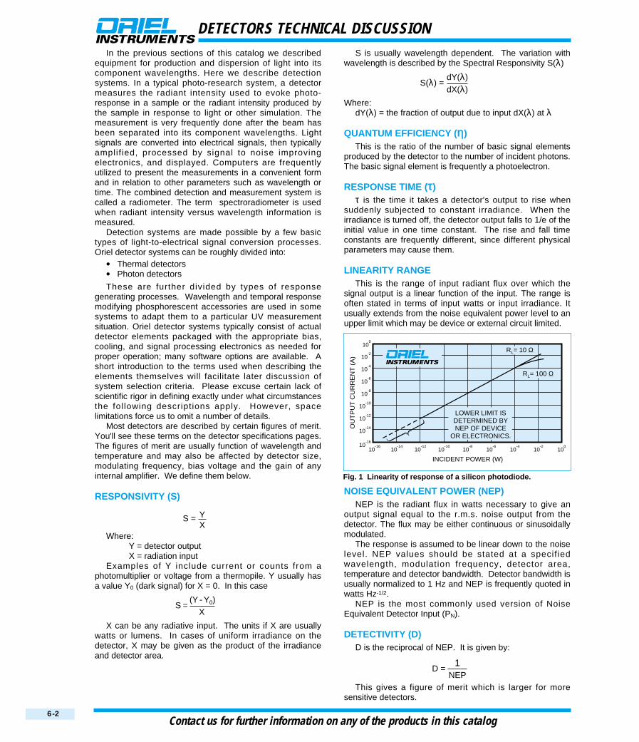
Most detectors are described by certain figures of merit.You'll see these terms on the detector specifications pages.The figures of merit are usually function of wavelength andtemperature and may also be affected by detector size,modulating frequency, bias voltage and the gain of anyinternal amplifier. We define them below.
RESPONSIVITY (S)
Where:Y = detector outputX = radiation input
Examples of Y include current or counts from aphotomultiplier or voltage from a thermopile. Y usually hasa value Y0 (dark signal) for X = 0. In this case
X can be any radiative input. The units if X are usuallywatts or lumens. In cases of uniform irradiance on thedetector, X may be given as the product of the irradianceand detector area.
S is usually wavelength dependent. The variation withwavelength is described by the Spectral Responsivity S(λ)
Where:dY(λ) = the fraction of output due to input dX(λ) at λ
QUANTUM EFFICIENCY (ηη)This is the ratio of the number of basic signal elements
produced by the detector to the number of incident photons.The basic signal element is frequently a photoelectron.
RESPONSE TIME (ττ)τ is the time it takes a detector's output to rise when
suddenly subjected to constant irradiance. When theirradiance is turned off, the detector output falls to 1/e of theinitial value in one time constant. The rise and fall timeconstants are frequently different, since different physicalparameters may cause them.
LINEARITY RANGEThis is the range of input radiant flux over which the
signal output is a linear function of the input. The range isoften stated in terms of input watts or input irradiance. Itusually extends from the noise equivalent power level to anupper limit which may be device or external circuit limited.
NOISE EQUIVALENT POWER (NEP)NEP is the radiant flux in watts necessary to give an
output signal equal to the r.m.s. noise output from thedetector. The flux may be either continuous or sinusoidallymodulated.
The response is assumed to be linear down to the noiselevel. NEP values should be stated at a specif iedwavelength, modulation frequency, detector area,temperature and detector bandwidth. Detector bandwidth isusually normalized to 1 Hz and NEP is frequently quoted inwatts Hz-1/2.
NEP is the most commonly used version of NoiseEquivalent Detector Input (PN).
DETECTIVITY (D)D is the reciprocal of NEP. It is given by:
This gives a figure of merit which is larger for moresensitive detectors.
DETECTORS TECHNICAL DISCUSSION
Contact us for further information on any of the products in this catalog6-2
INCIDENT POWER (W)
OU
TP
UT
CU
RR
EN
T (
A)
10-16
10-10
10-14
10-8
10-4
10-12
10-6
10-2
10010
-16
10-10
10-14
10-8
10-4
10-12
10-6
10-2
100
R = 10L Ω
R = 100L Ω
LOWER LIMIT ISDETERMINED BYNEP OF DEVICE
OR ELECTRONICS.
Fig. 1 Linearity of response of a silicon photodiode.
Y S = X
(Y - Y0)S = X
dY(λ)S(λ) =
dX(λ)
1D =
NEP

NORMALIZED DETECTIVITY (D*)For most detectors DAD
1/2 is constant; i.e., the detectivityvaries inversely with the square root of the area of thedetector. This is because the electrical noise power isusually proportional to the detector area AD, and current orvoltage, which provide a measure of that noise, areproportional to the square root of power. Similarly, becausemost detector noise is white noise, and white noise power isproportional to ∆f (where ∆f is the electrical bandwidth), thenoise signal is proportional to ∆f1/2.
D* is defined to allow comparison of different types ofdetectors independent of the detector area and bandwidth.
The units of D* are cm Hz1/2 W-1. Since D*, like NEP, isa function of wavelength and modulation frequency, it iscommon to see the normalized spectral responsivity D*(λ),or D*(λ ,f,∆f). Fig. 2 shows the D* of a number of ourdetectors.
NOISESo far we have not specified the nature of the noise
which limits the detectivity. There are several types:1. Shot noise2. Generation-recombination noise3. Johnson noise4. Flicker or 1/f noise5. Readout noise for array detectors
Shot Noise is due to the discrete nature of radiation,which is composed of photons arriving randomly in time.Absorbed photons produce photoelectrons at randomintervals, and this variation in current appears as noise.This noise can be generated by actual desired signalphotons or, in case of very low signal and very low noisedetectors, by background photon flux. When that occurs,the detector system is said to operate in a BackgroundLimited in Performance (BLIP) mode.
Generation-recombination Noise is seen in photo-conductors in which the absorbed photons produce bothpositive and negative charge carriers. Some of the freecarriers may recombine before they are collected. Thermalexcitation may generate additional carriers. Both thegeneration and recombination occur randomly, resulting innoise fluctuations in the output current.
Tel 203•377•8282 Fax 203•378•2457 E-Mail [email protected] URL www.oriel.com
Ligh
t Sou
rces
Phot
olith
ogra
phy
Lase
rsFT
-IRSp
ectro
met
ers
Mon
ochr
omat
ors
&Sp
ectro
grap
hsDe
tect
ion
Equi
pmen
tIn
stru
men
ts
6-3
Fibe
r Opt
ics
2 4 6 8 10 12
1E15
1E14
1E13
1E12
1E11
1E10
1E9
1E8
1E7
1E6
WAVELENGTH (µm)
D*
(cm
Hz
W)
1/2
-1
IDEAL CASE FOR PHOTOVOLTAIC DETECTORLIMITED BY 293K BACKGROUND
PMT
SiDIODE
InGaAsDIODE
PbS @ 243K
PbSe @ 243K
HgCdZnTe@ 243K
HgCdZnTe@ 293K
PYROELECTRIC
THERMOPILE
PDA
S1 PMT
CCD
Fig. 2 Approximate D* values as a function of wavelength for some detector types represented in this catalog.
TEMPERATURE EFFECTS
PHOTONNOISE
BIAS SUPPLYNOISE
DETECTORNOISE
DETECTOR
BIAS
AMPLIFIERAND SIGNAL
CONDITIONINGELECTRONICS DISPLAY
1 2 3 4 5
BACKGROUNDTHERMAL NOISE
POST DETECTION NOISEAND
DIGITIZATION NOISE
Fig. 3 System noise.
D* = D(AD1/2∆f1/2)
= D(AD ∆f)1/2
(AD ∆f)1/2=
NEP
Johnson Noise or thermal noise is caused by therandom motion of carriers in a conductor. The result isfluctuations in the detector’s internal resistance, or in anyresistance in series with the detector's terminals.
Flicker or 1/f Noise is not well understood. It occurs indetectors such as photoconductors which require a biasingcurrent. Its magnitude is proportional to 1/fB where B isusually between 0.8 and 1.2.
Readout Noise is a characteristic of array detectors andis associated with the uncertainties introduced during thetransfer of charges between storage registers.
In addition to the sources described above, detectorsignals can be subject to microphonic noise, caused byvibration or shock and by post detector electronic noise.Often the circuitry after the detector determine the lowestmeasurable signal, particularly for detectors which do notprovide some internal amplification of the photocurrent. Bycontrast, the almost noise-free internal amplification ofphotomultipliers accounts for their superb performance.
Finally, detectors are subject to temperature noisecaused by fluctuations in their temperature. This can be aproblem for small thermal detectors with low thermal mass.
CALIBRATIONThere are a lot of measurement situations when the
knowledge of the exact magnitude of an effect is notneeded. A relative reading is all that is necessary. In thatcase we only have to make sure that the inputs are higherthan the NEP level and lower than the damage level.Measurements become much simpler if the inputs are alsowithin the linear range of the detection system response.
However, when absolute measurements are required toquantify the light flux, calibrated instruments are needed.Oriel Instruments' Calibration Laboratory has acquired anumber of National Institute of Standards and Technology(NIST) source and detector calibration standards, as well asadditional standards traceable to international standards’setting and disseminating bodies. We are also in theenviable position of being able to utilize our own broadrange of products: UV and IR light sources, detectors,electronics, optics, positioning equipment, monochro-mators, spectrographs, and FT-IRs, to provide single pointor spectrally resolved calibration for most of the detectorproducts we ship. For some detectors we offer optionalPROMS that store a wavelength-responsivity table. Weuse our calibration transfer standards, lamps and detectors,typically traceable to the national Institute of Standards andTechnology (NIST) to ensure meaningful and reproduciblecalibrations.
THERMAL DETECTORSThermal detectors work by converting the incident
radiation into a temperature rise. The temperature changecan be measured in several ways. Our detectors use eitherthe voltage generated at the junction of dissimilar metals, orthe pyroelectric effect. In either case, we have a “sensitiveelement” where we measure temperature change.
We blacken the sensitive element to enhance theabsorption of the radiation. We choose the blackeningmaterial for its high and nearly uniform absorption, andhence detector responsivity, over a wide spectral range.This is a major advantage of thermal detectors.
The thickness of the black absorber is controlled to avoidadding excessive thermal mass to some detectors. Highthermal mass slows the response time and typicallyincreases NEP.
We offer two types of Thermal Detectors:
1. Thermopile Detectors for DC radiation.2. Pyroelectric Detectors for pulsed, chopped or
modulated radiation.
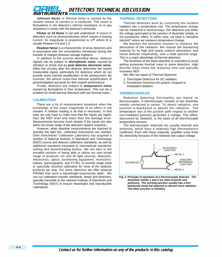
THERMOCOUPLESRadiation detecting thermopiles are based on
thermocouples. A thermocouple consists of two dissimilarmetals connected in series. To detect radiation, onejunction is blackened to absorb the radiation. Thetemperature rise of the junction (with respect to anothernon-irradiated junction) generates a voltage. This effect,discovered by Seebeck, is the basis of all thermocoupletemperature sensors.
The thermocouple materials are usually bismuth andantimony, which have a relatively high thermoelectriccoefficient. Even with these materials, amplifier noise limitsthe detectivity because of the relatively low output voltage.
DETECTORS TECHNICAL DISCUSSION
Contact us for further information on any of the products in this catalog6-4
METAL 2
METAL 1
BLACKENEDJUNCTION
SHIELDEDREFERENCEJUNCTION
VOLTMETER
Fig. 4 Principle of operation of a thermocouple detector. Thedissimilar metals 1 and 2 are often bismuth andantimony. The sensing junction usually has a thinblackened metal foil attached to absorb more radiation.The other junction is shielded.
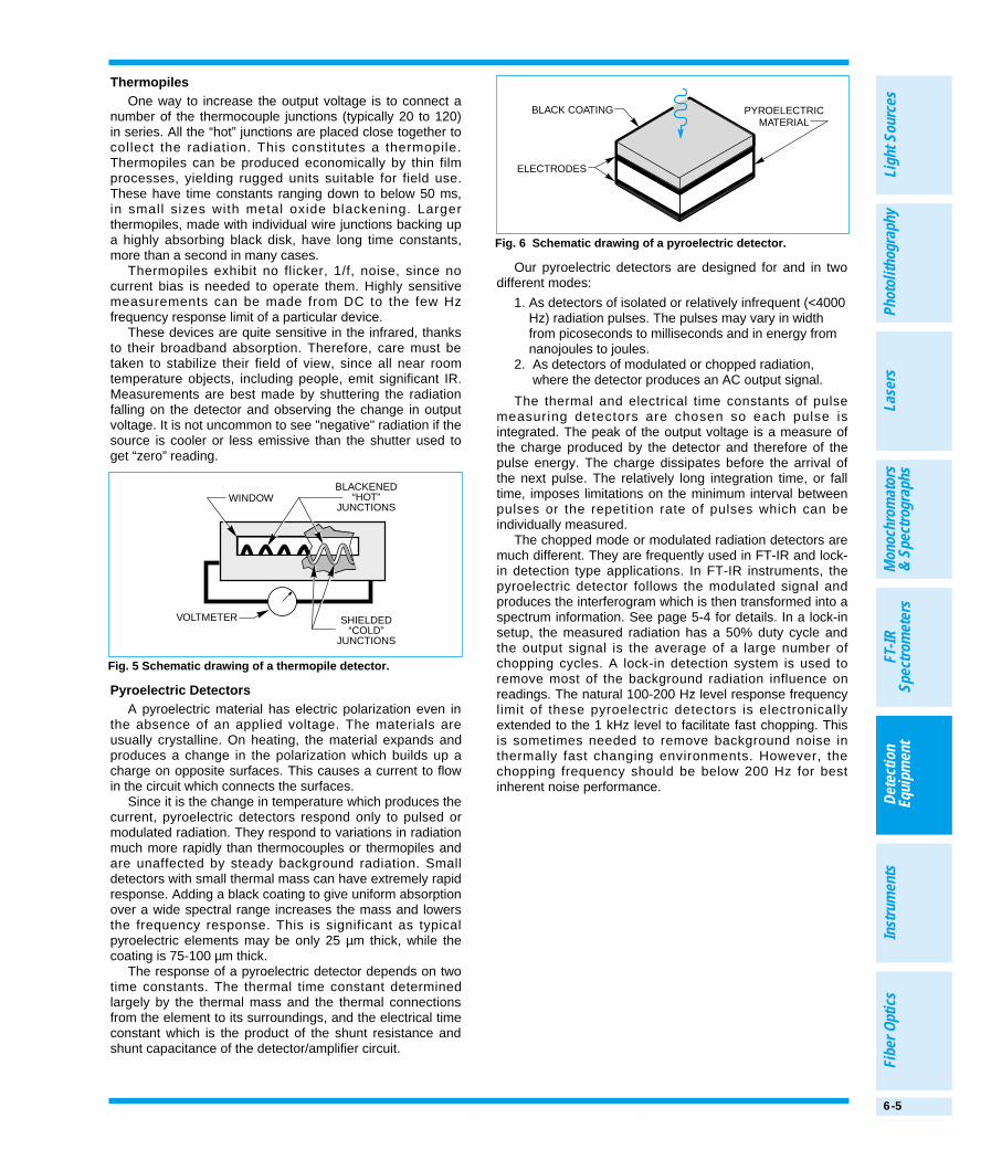
ThermopilesOne way to increase the output voltage is to connect a
number of the thermocouple junctions (typically 20 to 120)in series. All the “hot” junctions are placed close together tocollect the radiation. This constitutes a thermopile.Thermopiles can be produced economically by thin filmprocesses, yielding rugged units suitable for field use.These have time constants ranging down to below 50 ms,in small sizes with metal oxide blackening. Largerthermopiles, made with individual wire junctions backing upa highly absorbing black disk, have long time constants,more than a second in many cases.
Thermopiles exhibit no flicker, 1/f, noise, since nocurrent bias is needed to operate them. Highly sensitivemeasurements can be made from DC to the few Hzfrequency response limit of a particular device.
These devices are quite sensitive in the infrared, thanksto their broadband absorption. Therefore, care must betaken to stabilize their field of view, since all near roomtemperature objects, including people, emit significant IR.Measurements are best made by shuttering the radiationfalling on the detector and observing the change in outputvoltage. It is not uncommon to see "negative" radiation if thesource is cooler or less emissive than the shutter used toget “zero” reading.
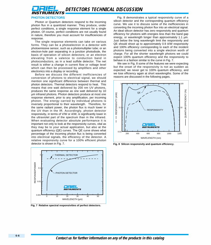
Pyroelectric DetectorsA pyroelectric material has electric polarization even in
the absence of an applied voltage. The materials areusually crystalline. On heating, the material expands andproduces a change in the polarization which builds up acharge on opposite surfaces. This causes a current to flowin the circuit which connects the surfaces.
Since it is the change in temperature which produces thecurrent, pyroelectric detectors respond only to pulsed ormodulated radiation. They respond to variations in radiationmuch more rapidly than thermocouples or thermopiles andare unaffected by steady background radiation. Smalldetectors with small thermal mass can have extremely rapidresponse. Adding a black coating to give uniform absorptionover a wide spectral range increases the mass and lowersthe frequency response. This is significant as typicalpyroelectric elements may be only 25 µm thick, while thecoating is 75-100 µm thick.
The response of a pyroelectric detector depends on twotime constants. The thermal time constant determinedlargely by the thermal mass and the thermal connectionsfrom the element to its surroundings, and the electrical timeconstant which is the product of the shunt resistance andshunt capacitance of the detector/amplifier circuit.
Our pyroelectric detectors are designed for and in twodifferent modes:
1. As detectors of isolated or relatively infrequent (<4000Hz) radiation pulses. The pulses may vary in widthfrom picoseconds to milliseconds and in energy fromnanojoules to joules.
2. As detectors of modulated or chopped radiation,where the detector produces an AC output signal.
The thermal and electrical time constants of pulsemeasuring detectors are chosen so each pulse isintegrated. The peak of the output voltage is a measure ofthe charge produced by the detector and therefore of thepulse energy. The charge dissipates before the arrival ofthe next pulse. The relatively long integration time, or falltime, imposes limitations on the minimum interval betweenpulses or the repetition rate of pulses which can beindividually measured.
The chopped mode or modulated radiation detectors aremuch different. They are frequently used in FT-IR and lock-in detection type applications. In FT-IR instruments, thepyroelectric detector follows the modulated signal andproduces the interferogram which is then transformed into aspectrum information. See page 5-4 for details. In a lock-insetup, the measured radiation has a 50% duty cycle andthe output signal is the average of a large number ofchopping cycles. A lock-in detection system is used toremove most of the background radiation influence onreadings. The natural 100-200 Hz level response frequencylimit of these pyroelectric detectors is electronicallyextended to the 1 kHz level to facilitate fast chopping. Thisis sometimes needed to remove background noise inthermally fast changing environments. However, thechopping frequency should be below 200 Hz for bestinherent noise performance.
Tel 203•377•8282 Fax 203•378•2457 E-Mail [email protected] URL www.oriel.com
Ligh
t Sou
rces
Phot
olith
ogra
phy
Lase
rsFT
-IRSp
ectro
met
ers
Mon
ochr
omat
ors
&Sp
ectro
grap
hsDe
tect
ion
Equi
pmen
tIn
stru
men
ts
6-5
Fibe
r Opt
ics
PYROELECTRICMATERIAL
BLACK COATING
ELECTRODES
Fig. 6 Schematic drawing of a pyroelectric detector.
WINDOWBLACKENED
“HOT”JUNCTIONS
SHIELDED“COLD”
JUNCTIONS
VOLTMETER
Fig. 5 Schematic drawing of a thermopile detector.
PHOTON DETECTORSPhoton or Quantum detectors respond to the incoming
photon flux in a quantized manner. They produce, underperfect conditions, a single response element for a singlephoton. Of course, perfect conditions are not usually foundin nature, therefore you must account for insufficiencies ofresponse.
The single response elements can take on variousforms. They can be a photoelectron in a detector withphotoemissive sensor, such as a photomultiplier tube; or anelectron-hole pair separating in a junction photodiode, thebasis of operation of silicon detectors; or an electronelevating from a valence to conduction band inphotoconductors, as in a lead sulfide detector. The netresult is either a change in current flow or voltage levelwhich can then be processed by amplifiers and otherelectronics into a display or recording.
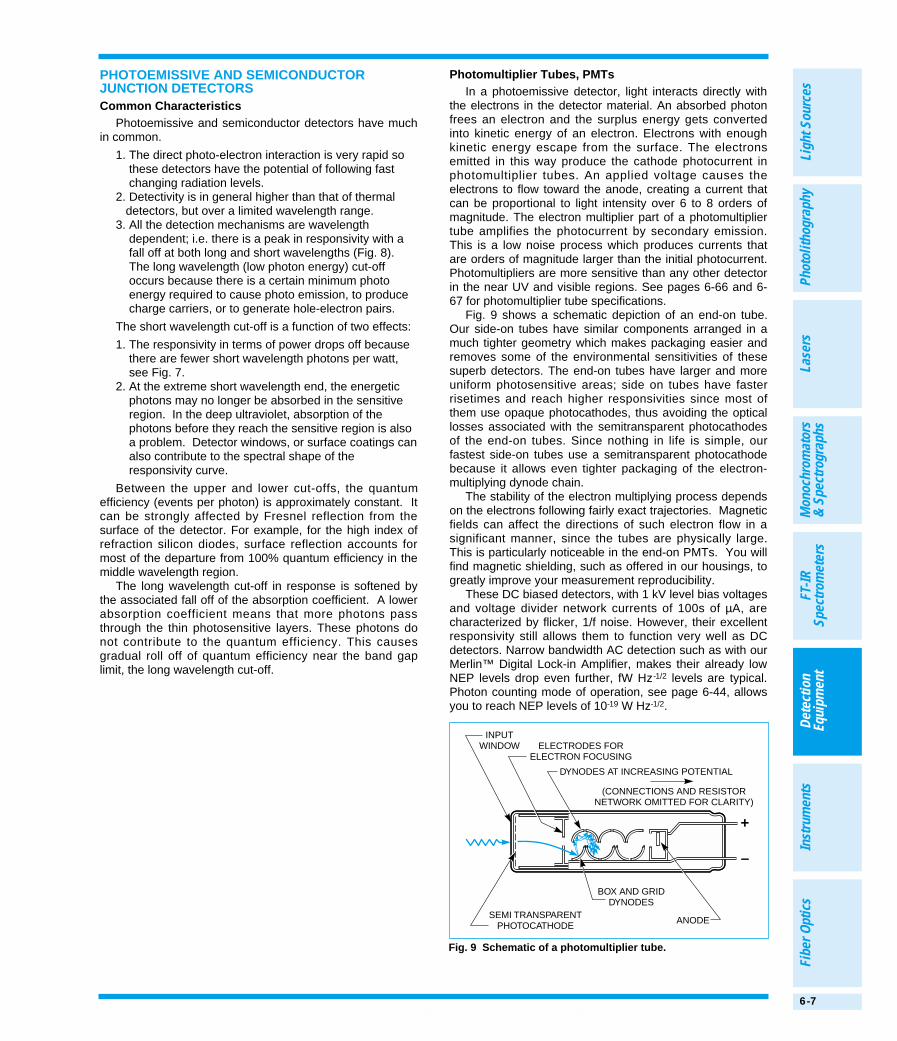
Before we discuss the different ineff iciencies ofconversion of photons to electrical signal, we shouldmention one significant difference between thermal andphoton detectors. Thermal detectors respond to heat. Thismeans that one watt delivered by 200 nm UV photons,produces the same response as one watt delivered by 10µm infrared photons. Photon detectors produce at most oneresponse element, prior to any amplification, per incomingphoton. The energy carried by individual photons isinversely proportional to their wavelength. Therefore, forthe same radiant power, the photon flux is much lower inthe UV than in the IR. Accordingly, photon detectorresponsivity, in terms of V/W or A/W, is significantly lower inthe ultraviolet part of the spectrum than in the infrared.When evaluating detector absolute performance it isimportant not only to look at the responsivity curves, vital asthey may be to your actual application, but also at thequantum efficiency (QE) curves. The QE curve shows whatpercentage of the incoming photon flux is being convertedinto electrical signals, the efficiency of the detector. Arelative responsivity curve for a 100% efficient photondetector is shown in Fig. 7.
Fig. 8 demonstrates a typical responsivity curve of asilicon detector and the corresponding quantum efficiencycurve. We use it to discuss some of the inefficiencies inconverting the incoming photon flux into an electrical signal.An ideal silicon detector has zero responsivity and quantumefficiency for photons with energies less than the band gapenergy, or wavelength longer than approximately 1.1 µm.Just below the long wavelength limit the responsivity andQE should shoot up to approximately 0.9 A/W responsivityand 100% efficiency corresponding to each of the incidentphotons being converted into a single electron worth ofcharge. For all the shorter wavelength photons we couldexpect 100% quantum efficiency and the responsivity tobehave in a fashion similar to the curve in Fig. 7.
We see in Fig. 8 some of the features we were expectingbut the onset of the responsivity is not as sudden asexpected; we never get to 100% quantum efficiency, andwe lose efficiency again at short wavelengths. Some of thereasons are discussed in the following pages.
DETECTORS TECHNICAL DISCUSSION
Contact us for further information on any of the products in this catalog6-6
200 400 600 800 1000 1200
WAVELENGTH (nm)
1
0.1
0.01
100
10
1
QE
RESPONSIVITY
RE
SP
ON
SIV
ITY
(A
/W)
QU
AN
TU
M E
FF
ICIE
NC
Y (
%)
Fig. 8 Silicon responsivity and quantum efficiency.
0 10 20 30 40 50
WAVELENGTH (µm)
1
0.1
0.01
0.001
RE
SP
ON
SE
/PO
WE
R
PHOTON DETECTOR
THERMAL DETECTOR
Fig. 7 Relative spectral responsivities of perfect detectors.
PHOTOEMISSIVE AND SEMICONDUCTORJUNCTION DETECTORSCommon Characteristics
Photoemissive and semiconductor detectors have muchin common.
1. The direct photo-electron interaction is very rapid sothese detectors have the potential of following fastchanging radiation levels.
2. Detectivity is in general higher than that of thermaldetectors, but over a limited wavelength range.
3. All the detection mechanisms are wavelengthdependent; i.e. there is a peak in responsivity with afall off at both long and short wavelengths (Fig. 8).The long wavelength (low photon energy) cut-offoccurs because there is a certain minimum photoenergy required to cause photo emission, to producecharge carriers, or to generate hole-electron pairs.
The short wavelength cut-off is a function of two effects:
1. The responsivity in terms of power drops off becausethere are fewer short wavelength photons per watt,see Fig. 7.
2. At the extreme short wavelength end, the energeticphotons may no longer be absorbed in the sensitiveregion. In the deep ultraviolet, absorption of thephotons before they reach the sensitive region is alsoa problem. Detector windows, or surface coatings canalso contribute to the spectral shape of theresponsivity curve.
Between the upper and lower cut-offs, the quantumefficiency (events per photon) is approximately constant. Itcan be strongly affected by Fresnel reflection from thesurface of the detector. For example, for the high index ofrefraction silicon diodes, surface reflection accounts formost of the departure from 100% quantum efficiency in themiddle wavelength region.
The long wavelength cut-off in response is softened bythe associated fall off of the absorption coefficient. A lowerabsorption coefficient means that more photons passthrough the thin photosensitive layers. These photons donot contribute to the quantum efficiency. This causesgradual roll off of quantum efficiency near the band gaplimit, the long wavelength cut-off.
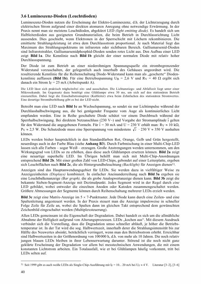
Photomultiplier Tubes, PMTsIn a photoemissive detector, light interacts directly with
the electrons in the detector material. An absorbed photonfrees an electron and the surplus energy gets convertedinto kinetic energy of an electron. Electrons with enoughkinetic energy escape from the surface. The electronsemitted in this way produce the cathode photocurrent inphotomultiplier tubes. An applied voltage causes theelectrons to flow toward the anode, creating a current thatcan be proportional to light intensity over 6 to 8 orders ofmagnitude. The electron multiplier part of a photomultipliertube amplifies the photocurrent by secondary emission.This is a low noise process which produces currents thatare orders of magnitude larger than the initial photocurrent.Photomultipliers are more sensitive than any other detectorin the near UV and visible regions. See pages 6-66 and 6-67 for photomultiplier tube specifications.
Fig. 9 shows a schematic depiction of an end-on tube.Our side-on tubes have similar components arranged in amuch tighter geometry which makes packaging easier andremoves some of the environmental sensitivities of thesesuperb detectors. The end-on tubes have larger and moreuniform photosensitive areas; side on tubes have fasterrisetimes and reach higher responsivities since most ofthem use opaque photocathodes, thus avoiding the opticallosses associated with the semitransparent photocathodesof the end-on tubes. Since nothing in life is simple, ourfastest side-on tubes use a semitransparent photocathodebecause it allows even tighter packaging of the electron-multiplying dynode chain.
The stability of the electron multiplying process dependson the electrons following fairly exact trajectories. Magneticfields can affect the directions of such electron flow in asignificant manner, since the tubes are physically large.This is particularly noticeable in the end-on PMTs. You willfind magnetic shielding, such as offered in our housings, togreatly improve your measurement reproducibility.
These DC biased detectors, with 1 kV level bias voltagesand voltage divider network currents of 100s of µA, arecharacterized by flicker, 1/f noise. However, their excellentresponsivity still allows them to function very well as DCdetectors. Narrow bandwidth AC detection such as with ourMerlin™ Digital Lock-in Amplifier, makes their already lowNEP levels drop even further, fW Hz-1/2 levels are typical.Photon counting mode of operation, see page 6-44, allowsyou to reach NEP levels of 10-19 W Hz-1/2.
Tel 203•377•8282 Fax 203•378•2457 E-Mail [email protected] URL www.oriel.com
Ligh
t Sou
rces
Phot
olith
ogra
phy
Lase
rsFT
-IRSp
ectro
met
ers
Mon
ochr
omat
ors
&Sp
ectro
grap
hsDe
tect
ion
Equi
pmen
tIn
stru
men
ts
6-7
Fibe
r Opt
ics
INPUTWINDOW
SEMI TRANSPARENTPHOTOCATHODE
ELECTRODES FORELECTRON FOCUSING
DYNODES AT INCREASING POTENTIAL
(CONNECTIONS AND RESISTORNETWORK OMITTED FOR CLARITY)
_+
BOX AND GRIDDYNODES
ANODE
Fig. 9 Schematic of a photomultiplier tube.

Junction PhotodiodesThere are several ways of classifying semiconductor
detectors. All are photoconductive, but here we use thephotoconductive detectors' name for devices which rely onphotoconductivity in the bulk and do not necessarily havejunctions. We will talk more about them on page 6-10.
Junction detectors (or photodiodes) have a p-n junctionformed in them. Many junction detectors can be used in thephotovoltaic mode without a bias, or in the photoconductivemode when a reverse bias is applied. They can alsoprovide photocurrent amplification through an avalancheionization process when back biased at near breakdownvoltage in properly designed structures.
In the photovoltaic mode, the electron-hole pairs(produced by photon absorption) migrate to opposite sidesof the junction thus producing a voltage (and also a current,if the device is connected in a circuit).
In the photoconductive mode, a reverse bias is appliedacross the junction. Light produces electron-hole pairswhich greatly increase the conductance. The currentproduced by the bias and free carriers is proportional to thelight intensity over a wide range.
Silicon PhotodiodesSilicon photodiodes are the most common detectors of
light used in instrumentation. The spectral response (Fig. 8on page 6-6) covers the UV, the visible and the nearinfrared. The linearity and dynamic range are excellent (Fig.1 on page 6-2); getting a signal is simple.
Fig. 10 shows the typical structure of a si l iconphotodiode. Photons pass through the thin top layer togenerate electrons and holes near the junction. Thejunction is a region depleted of current carriers, bothelectrons and holes, by the gradients of the potentialsassociated with the energy bands. It is formed between thep and n type silicon. The junction drives holes into the pmaterial and the electrons into the n material. This results ina voltage difference between the two regions, and if theyare connected by external circuitry, a current.
Unbiased Operation - Photovoltaic ModeBecause the 1/f noise increases with bias, this mode has
the better NEP at low frequencies. In fact the signal to noiseratio is better than that for biased operation at frequenciesbelow 100 kHz and much better below 1 kHz.
Biased Operation - Photoconductive ModeOperation with reverse bias reduces junction
capacitance and thus increases the speed of response ofthe diode. It is the preferred mode of operation for pulseddetectors.
Linear RangeSilicon diodes require a low impedance load resistor to
provide a linear output in a photovoltaic mode. This makesthe maximum output voltage too low to achieve widedynamic range when using an oscilloscope as a monitor. Atransimpedance amplifier solves the major linearityrestrictions, by providing near "zero" load impedance, andproduces higher output voltages. It also limits the highfrequency response of the system.
Wide range linear performance is much easier toachieve in the back biased mode of operation. Linear outputpersists almost all the way to bias voltage allowing easydisplay on an oscilloscope. We provide 6 V back bias fromlong life lithium batteries for our biased detectors.
GaNThese wide band gap diodes offer UV sensitivity
while they reject VIS-IR background, thus facilitatingmeasurements in this difficult wavelength range.
InSbThese liquid Nitrogen cooled detectors, used with
our FT-IR instruments, on page 5-19, offer ultimateperformance in the 2 to 5 µm range.
Ge, InGaAs, Extended InGaAs PhotodiodesJust about everything we said about silicon detectors
can also be said about the these diodes. They find mostapplications in the NIR, 0.8 to 2.5 µm. Their noiseperformance does not match that of Si and therefore weoffer TE cooled versions of them, besides the roomtemperature ones.
HgCdZnTe PhotodiodesThings get even more confusing as far as junction
photoconductors vs bulk photoconductors with these smallband gap IR photodetectors. However, at least one roomtemperature implementation of these detectors doesfunction in a photovoltaic mode and thus deserves to belisted in this section. Their current biased versions fit betterwith the PbS and PbSe photoconductors than with backbiased junction diodes. Therefore we talk about them a littlemore in that section, page 6-75.
We offer these detectors for the 2 to 12 µm wavelengthrange. Optical immersion is offered with most of them totake better advantage of the detector active area.
DETECTORS TECHNICAL DISCUSSION
Contact us for further information on any of the products in this catalog6-8
ACTIVE AREA
p AREA+
DEPLETIONREGION
n TYPE SILICON
n MATERIAL(FOR CONTACT)
-
METAL CONTACT
SYMBOLICFORM
Fig. 10 Model of a silicon photodiode. The junction betweenthe p+ and depletion regions give this detector itsname.

MULTICHANNEL DETECTORSThe detectors we've been describing until now are single,
discrete devices. Now we talk about multichannel detectors -photodiode arrays and charge coupled devices. The majordifferences between them lie in sizes of sensitive elements orpixels, the linear versus two dimensional value of the arrays,and the signal handling and readout methods. OurLineSpec™ and most of our InstaSpec™ family ofmultichannel detectors (pages 6-106 to 6-119) utilize siliconas a detector and are therefore sensitive in the 200 to 1100nm spectral range. We now also offer InGaAs PDAs (pages6-120 to 6-123) which are sensitive from 800 to 1700 nm.
The most useful arrays, and the only kind in our catalog,are of a self scanning type. This means that individualdetector elements, and their associated circuitry, integratethe incident photon flux for some time and then are read outin a serial fashion. This is significantly different from the realtime operation of single element detector systems. This selfscanning mode of operation limits the nine or ten orders ofmagnitude dynamic range of individual photodiodes to amore practical three to five orders of magnitude, devicedependent. High density packing of the smallphotosensitive pixels, to minimize non-photoresponsiveareas and provide high resolution, limits the capacity of thecharge storing structures. The major benefit of this chargestorage capability is that usually only a single data channelis needed to read the information from all the spectral orimaging channels.
All of the arrays share the major advantage ofmultichannel or multiplexing capability. They make possiblean almost instantaneous acquisition of one or more fullspectroradiometric data sets when coupled to a standard orimaging spectrograph. The traditional technique would haveinvolved mechanical scanning of one or more mono-chromators to sequentially bring various wavelengths oflight to the single detector location.
Photodiode Arrays (PDAs)Our PDAs are of a linear format. The aspect ratio of
individual pixels, 25 µm wide by 25 mm high for the siliconbased models, and 50 µm wide by 200 µm high for theInGaAs models, is designed to complement spectrographfunction. Narrow width gives high resolution; significantheight allows more signal collection. They operate in aphotoconductive mode. The individual diode elementsrespond to the photon flux by producing photocurrents.Those in turn charge individual storage capacitors. Thecapacitors are read and discharged by on-chip circuitry andthe information is fed out in a timed sequence.
Integration t ime becomes a new and signif icantparameter when setting up your measurement with thearrays. Dark current plays a more significant role with thesestoring detectors, since with very long integration times youmay reach full capacity of all the storage elements and thuswipe out all the useful information. A concept of saturationtime is used to describe this phenomenon. Fig. 11 showstypical temperature dependence of saturation time forPDAs.
We offer a number of PDA based systems. Compared toCCDs, their advantage is lower cost and higher lightexposure capability. Their disadvantage involves higherreadout noise, hundreds of thousands of electrons perchannel, which limits their ultimate detectivity.
LineSpec™ Charge Coupled Devices (CCDs)These inexpensive linear CCD detectors, with 14 x 14 µm
or 14 x 200 µm pixels, allow high speed, low cost datacollection, for intermediate illumination level applications.
InstaSpec™ Charge Coupled Devices (CCDs)These two dimensional arrays offer different electronic
construction than PDAs. They are characterized byextremely low readout noise, down to a few electrons worthper pixel, and good separation between signal channels -no blooming. Nothing in life being free, they are somewhatmore expensive than PDAs.
Typical pixel elements are 27 µm square. Softwareoptions allow you to take advantage of the two dimensionalnature of CCDs for a spectroscopic form of imaging. (Youcould use them for standard high light level imaging, but avideo recorder tube can do that for significantly lower cost.)Fig. 12 shows this spectroscopic “imaging”. Multiple,spatially separated inputs illuminate the entrance slit of animaging spectrograph. The spectrally resolved image of thesources illuminates the CCD at the output plane of thespectrograph. Multiple spectra, e.g. of excitation andvarious responses, can then be displayed simultaneouslyfor comparison and analysis.
Tel 203•377•8282 Fax 203•378•2457 E-Mail [email protected] URL www.oriel.com
Ligh
t Sou
rces
Phot
olith
ogra
phy
Lase
rsFT
-IRSp
ectro
met
ers
Mon
ochr
omat
ors
&Sp
ectro
grap
hsDe
tect
ion
Equi
pmen
tIn
stru
men
ts
6-9
Fibe
r Opt
ics
8 10 12 14 16 18 20 22 24 26
1000
800
600
400
200
TEMPERATURE ( C)o
SAT
UR
ATIO
NT
IME
(s)
-30 -20 -10 0 10 20 30
8
6
4
2
0
TEMPERATURE ( C)o
SAT
UR
ATIO
NT
IME
(H
RS
)
Fig. 11 PDA saturation time vs temperature.
Fig. 12 Fibers imaged through the MS260i™ ImagingSpectrograph, and captured with InstaSpec™ IV CCD.

PHOTOCONDUCTIVE DETECTORSIn photoconductive detectors, absorbed incident photons
produce free charge carriers. These change the electricalconductivity of the detector. An applied voltage, or bias,causes a current to flow which is proportional to the photonirradiance (it helps if the dark resistance is very high). Leadsulfide and lead selenide are examples of this type ofdetector. Fig. 13 shows this concept.
PbS and PbSe detectors are fabricated by chemicallydepositing polycrystalline film on a quartz substrate. Goldelectrodes are plated to the edges of the film to provideelectrical contact and the whole assembly is sealed inside apackage with an appropriate window, quartz or sapphire.See Fig. 14. The cooled lead salt detectors also include theTE cooling stages and a thermistor sensor inside of thehousing. This minimizes the cooling requirements, since thehousing minimizes heat transfer from the environment tothe detector element. The heat being generated by the TEcoolers also protects the window from condensation.
Liquid Nitrogen cooled MCT detectors, used in our MIR8000™ FT-IR instruments, page 5-21, offer ultimatedetectivity in the 2 to 17 µm range. The TE cooledHgCdZnTe family offers somewhat lower performance, butremoves the need for liquid nitrogen refilling.
The epitaxially grown HgCdZnTe family of detectors ischaracterized by low impedance, but when properly biasedand interfaced also provides linear performance. Thisversatile room and near room temperature operation familyof detectors does not exactly fit either the junction or bulkphotoconductor description. However, it is similar to one orthe other in its different modes of operation. In thephotoconductive mode of operation it is characterized bysignificantly faster risetimes than the lead salt detectors,especially at longer wavelengths.
Bias requirements, and the associated heating, as wellas noise generation is smaller in smaller detectors. Oneway to make a small detector look optically like a bigdetector is through the use of optical immersion, Fig. 15.
This approach makes the detector surface look n² timeslarger, where n is the index of refraction of the lens, for thehyperspherical lens shape used in our optically immerseddetectors. The monolithic construction of these detectors,(the epitaxial layer is grown directly on the lens substrate)makes this approach highly effective for HgCdZnTedetectors.
DETECTORS TECHNICAL DISCUSSION
Contact us for further information on any of the products in this catalog6-10
LENS
OPTICALAREA
ELECTRICALAREA
Fig. 15 Principle of optical immersion.
2.0 4.0 6.0 8.0 10.0 12.0
1E11
1E10
1E9
1E8
D*
(cm
Hz
W)
1/2
-1
WAVELENGTH (µm)
PbS
PbSe
HgCdZnTe
Fig. 16 Typical detectivities of some of our cooled IRdetectors.
.029(0.15)
WL
GOLD ELECTRODE
QUARTZ ORSAPPHIRE WINDOW
PbS ACTIVEAREA
QUARTZSUBSTRATE
.006 CU CLADSTEEL WIRE
HERMETICALLYSEALED
TO-5 CASE
Fig. 14 Typical lead salt detector.
DEPOSITEDPHOTOCONDUCTOR
SUBSTRATE
V
Fig. 13 Schematic of a photoconductive detector.
Dimensions in inches (mm)
40
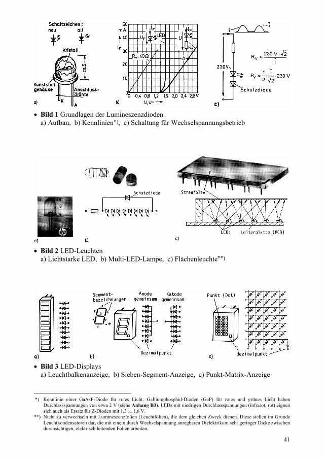
3.6 Lumineszenz-Dioden (Leuchtdioden) Lumineszenz-Dioden nutzen die Erscheinung der Elektro-Lumineszenz, d.h. der Lichterzeugung durch elektrischen Strom aufgrund einer direkten atomaren Anregung ohne notwendige Erwärmung. In der Praxis nennt man sie meistens Leuchtdioden, abgekürzt LED (light emitting diode). Es handelt sich um Halbleiterdioden aus geeigneten Grundmaterialien, die beim Betrieb in Durchlassrichtung Licht aussenden. Dies geschieht, wenn Elektronen in der Sperrschicht mit Löchern rekombinieren. Die emittierte Strahlungsleistung ist etwa dem Durchlassstrom proportional. Je nach Material liegt das Maximum des Strahlungsspektrums im infraroten oder sichtbaren Bereich. Galliumarsenid-Dioden sind Infrarotstrahler, Galliumarsenidphosphid-Dioden senden rotes Licht aus. Den Aufbau einer LED zeigt Bild 1a. Die Kennlinie nach Bild 1b gleicht der einer normalen Diode mit relativ hoher Durchlassspannung.Der Diode ist zum Betrieb an einer niederohmigen Spannungsquelle ein strombegrenzender Widerstand vorzuschalten, der gelegentlich auch innerhalb des Gehäuses angeordnet wird. Die resultierende Kennlinie für die Reihenschaltung Diode-Widerstand kann man als „gescherte“ Dioden-kennlinie auffassen (Bild 1b). Für eine Betriebsspannung UB = 2,6 V und RV = 40 ergibt sich danach ein Strom IF = 25 mA (Arbeitspunkt A).
Die LED lässt sich praktisch trägheitsfrei ein- und ausschalten. Die Lichtanstiegs- und Abfallzeit liegt unter einer Mikrosekunde. Im Gegensatz dazu benötigt eine Glühlampe etwa 30 ms, um sich auf den stationären Betrieb einzustellen. Dabei liegt die Einschaltstromspitze (Kaltleiter) etwa beim Zehnfachen des stationären Stromwertes. Eine derartige Stromüberhöhung gibt es bei der LED nicht.
Betreibt man eine LED nach Bild 1c an Wechselspannung, so sendet sie nur Lichtimpulse während der Durchlasshalbschwingung aus, die bei genügender Frequenz vom Auge als kontinuierliches Licht empfunden werden. Eine in Reihe geschaltete Diode schützt vor einem Durchbruch während der Sperrhalbschwingung. Bei direktem Netzanschluss (230 V~) und Vorgabe der Stromamplitude i gelten für den Widerstand die angegebenen Formeln. Für i = 30 mA und U = 230 V erhält man: RV 10 k ,PV 2,5 W. Die Schutzdiode muss eine Sperrspannung von mindestens 2 · 230 V 350 V aushalten können.LEDs werden bisher hauptsächlich in den Standardfarben Rot, Orange, Gelb und Grün hergestellt, neuerdings auch in der Farbe Blau (siehe Anhang B3). Durch Farbmischung in einer Multi-Chip-LED lassen sich alle Farben – sogar Weiß – erzeugen. Große Anstrengungen werden unternommen, um den Wirkungsgrad von LEDs so zu erhöhen, dass diese auch Glühlampen ersetzen können. Bild 2a zeigt eine neuartige superhelle LED. Im Übrigen behilft man sich mit Multi-Chip-Anordnungen entsprechend Bild 2b. Mit einer großen Zahl von LED-Chips, gebondet auf einer Leiterplatte, ergeben sich Leuchtflächen nach Bild 2c, die als Hintergrundbeleuchtung (Backlight) für Anzeigen dienen1).Anzeigen sind das Hauptanwendungsgebiet für LEDs. Sie werden dazu in vielfältiger Weise zu Anzeigeeinheiten (Displays) kombiniert. In einfacher Aneinanderreihung nach Bild 3a ergeben sie eine Leuchtbalkenanzeige (Bar graph), die als grobe Analogwertanzeige dienen kann. Bild 3b zeigt die bekannte Sieben-Segment-Anzeige mit Dezimalpunkt. Jedes Segment wird in der Regel durch eine LED gebildet, wobei entweder die einzelnen Anoden oder Katoden zusammengeschaltet werden. Größere Abmessungen der Segmente können durch Reihenschaltung mehrerer LEDs erzielt werden.
Bild 3c zeigt eine Matrix-Anzeige im 5 7-Punktraster. Jede Diode kann durch eine Zeilen- und eine Spaltenleitung angesteuert werden. In der Praxis steuert man die Anzeige impulsweise in schneller Folge Zeile für Zeile an, wobei die Spalten dann im gleichen Takt entsprechend dem gewünschten Zeichenbild eingeschaltet werden (Multiplexsteuerung). Allen LEDs gemeinsam ist die Eigenschaft der Degradation. Dabei handelt es sich um die allmähliche Abnahme der Helligkeit aufgrund von Alterungsprozessen. LEDs „kochen aus“. Mit diesem Ausdruck verbindet sich die Vorstellung, dass die Degradation umso schneller abläuft, je höher die Betriebs-temperatur ist. In der Tat wird die sog. Halbwertszeit, innerhalb derer die Strahlungsintensität bis zur Hälfte des Neuwertes absinkt, beträchtlich verringert, wenn man den Betriebsstrom erhöht. Erreichbar sind Halbwertszeiten in der Größenordnung von 100000 h, d.h. von mehr als 10 Jahren. Die noch relativ jungen blauen LEDs bleiben in ihrer Lebenserwartung darunter. Störend ist die noch nicht ganz geklärte Erscheinung der Degradation vor allem bei messtechnischen Anwendungen, die mit einem konstanten Lichtstrom arbeiten. Ein Totalausfall, wie er bei Glühlampen häufig vorkommt, tritt bei LEDs selten auf.
1) Seit 1999 gibt es auch weiße LEDs als Single-Chip-Ausführung mit IF = 10... 20 mA bei UF 4 V. Literatur [3–2], [3–6]
41
Bild 1 Grundlagen der Lumineszenzdiodena) Aufbau, b) Kennlinien*), c) Schaltung für Wechselspannungsbetrieb
Bild 2 LED-Leuchtena) Lichtstarke LED, b) Multi-LED-Lampe, c) Flächenleuchte**)
Bild 3 LED-Displaysa) Leuchtbalkenanzeige, b) Sieben-Segment-Anzeige, c) Punkt-Matrix-Anzeige
*) Kennlinie einer GaAsP-Diode für rotes Licht. Galliumphosphid-Dioden (GaP) für rotes und grünes Licht haben
Durchlassspannungen von etwa 2 V (siehe Anhang B3). LEDs mit niedrigen Durchlassspannungen (infrarot, rot) eignen sich auch als Ersatz für Z-Dioden mit 1,3 ... 1,6 V.
**) Nicht zu verwechseln mit Lumineszenzfolien (Leuchtfolien), die dem gleichen Zweck dienen. Diese stellen im Grunde Leuchtkondensatoren dar, die mit einem durch Wechselspannung anregbaren Dielektrikum sehr geringer Dicke zwischen durchsichtigen, elektrisch leitenden Folien arbeiten.

276
17 Optoelektronik
17.1 Fototransistoren und Fotothyristoren Unter Optoelektronik versteht man das Anwendungsgebiet aller elektronischen Bauelemente, die Licht in ein elektrisches Signal umformen bzw. die umgekehrte Funktion ausüben. Da es sich dabei häufig nur um Varianten konventioneller Bauelemente handelt, wurden einige bereits im vorangegan-genen Text besprochen: Fotowiderstände, Fotodioden bzw. Fotoelemente, Leuchtdioden, Anzeige-bausteine und Bildröhren. Im Folgenden sollen Fototransistoren und -thyristoren behandelt werden. Unter einem Fototransistor versteht man normalerweise einen npn-Bipolartransistor, bei dem die Basis-Kollektor-Diode als Fotodiode ausgebildet ist. Man stellt sich daher nach Bild 1a den Fototransistor vor als einen normalen Transistor mit einer zugeschalteten Fotodiode. Der Basis-anschluss ist grundsätzlich nicht erforderlich, wird aber dennoch oft angelegt, um zusätzlich eine elektrische Steuerung vornehmen zu können. Der Fotostrom seinerseits wirkt wie ein interner licht-gesteuerter Basisstrom und erscheint mit dem Stromverstärkungsfaktor B – genau genommen 1 + B – multipliziert als Kollektorstrom IC. Bei reiner Lichtsteuerung ergibt sich damit qualitativ eine Kennlinienschar nach Bild 1b. Der dort auftretende Dunkelstrom ist identisch mit dem üblichen Reststrom ICEO = (1 + B) · ICBO1 ).Bild 1c zeigt Ausführungsformen und Schaltzeichen von Fototransistoren. Dort wird auch der häufig vorkommende Foto-Darlingtontransistor angegeben, der wegen der zusätzlichen Stromverstärkung durch den nachgeschalteten Transistor eine besonders hohe Lichtempfindlichkeit besitzt, leider aber auch eine erhöhte Temperaturempfindlichkeit. Fototransistoren werden zumeist im Schaltbetrieb eingesetzt, wobei sie von Lichtimpulsen aufgesteuert werden. Das geschieht im Bild 2 durch eine nahe benachbarte LED. Beim Schalten des Diodenstromes IF mit dem Transistor T wird der von der Diode gesendete Lichtstrom ein- und abgeschaltet. Entsprechend steigt und fällt der Kollektorstrom des Fototransistors, der wegen der offenen Basis mit dem jeweiligen Emitterstrom identisch ist. Es treten Schaltzeiten auf wie beim normalen Bipolartransistor: Anstiegs- und Abfallzeiten sowie eine Speicherzeit tS2). Damit ergeben sich die angegebenen Zeitverläufe für die Spannung u2, wonach man die Flankenzeiten näherungs-weise durch eine Konstante beschreiben kann. Diese wird hauptsächlich bestimmt durch den angegebenen Arbeitswiderstand R und eine mit der Stromverstärkung B hochtransformierte Basis-Kollektorkapazität:
= R · CBC · B = 2k ·5pF ·200 = 2µs für die Werte R = 2 k , CBC = 5pF und B = 200. Die Basis-Kollektor-Kapazität CBC wird beim Schaltbetrieb jeweils umgeladen. Bezogen auf die Kollektor-Emitter-Strecke, erscheint sie um den Faktor B erhöht, weil der kapazitive Strom genau wie der Fotostrom mit diesem Faktor vervielfacht wird. Da man den Kollektor-Basis-Übergang im Interesse einer guten Fotoempfindlichkeit großflächiger ausbildet als bei normalen Transistoren, ist die Kapazität CBC auch relativ groß. Deshalb erreicht man eine niedrige Zeitkonstante nur über einen kleinen Arbeitswiderstand R, beispielsweise durch die Zwischenschaltung eines Transistors T2 in Basisschaltung nach Bild 2c mit R = 1/s, wobei s die Steilheit des Transistors T2 ist. Die Speicherzeit ts ist auch hier eine Funktion der Sättigung und hängt ab von dem Grad der Übersteuerung, d.h. von der Beleuchtungsstärke. Man kann die Speicherzeit verringern durch einen Widerstand (> 10 k ) zwischen Basis und Emitter, über den die Basis schneller ausgeräumt wird. Ein derartiger Widerstand verringert allerdings auch die Fotoempfindlichkeit, da er den Fotostrom Ip teilweise nach außen ableitet. Leider wird damit bei unveränderter Beleuchtung das Aufsteuern des Transistors verlangsamt. Das Sperren wird jedoch stets beschleunigt.
Ein praktisch bedeutendes optoelektronisches Bauelement ist auch der Fotothyristor nach Bild 3a. Erunterscheidet sich von einem normalen Thyristor im Wesentlichen nur dadurch, dass die gemeinsame Basis-Kollektor-Sperrschicht der beiden integrierten Transistoren als Fotodiode ausgebildet ist3). Über einen intern oder extern angeordneten Widerstand RGK kann man einen Teil des Fotostromes IPableiten und somit die Zündempfindlichkeit einstellen. Fotothyristoren sind als diskrete Bauelemente nur selten anzutreffen. Man verwendet sie meistens als Schaltglied in Verbindung mit einer LED in Optokopplern. Das gilt im besonderen Maße für den „Foto-Triac“ nach Bild 3b, der als Antiparallelschaltung zweier Fotothyristoren einen lichtgesteuerten Wechselstromschalter darstellt4).
1) Siehe Gleichstromersatzbild im Abschnitt 10.3. 2) Zu den Schaltzeiten vgl. Abschnitt 10.4.3) Zur Funktion eines Thyristors siehe Abschnitt 14.11.4) Zu entsprechenden Optokopplern siehe Anhang B17; zum Triac siehe Abschnitt 19.5.

277
Bild 1 Fototransistorena) Ersatzbild, b) Kennlinien, c) Ausführungsformen und Schaltzeichen
Bild 2 Schaltverhalten des Fototransistors**)
a) Emitterschaltung, b) Kollektorschaltung, c) Kaskodeschaltung
Bild 3 Fotothyristor und Fototriac a) Fotothyristor, b) Fototriac
*) Für die Darstellung des Gleichstromverhaltens insgesamt verwendet man zweckmäßig das Ersatzbild nach Abschnitt
10.3, das um eine Stromquelle mit dem Fotostrom zu ergänzen ist. **) Die im Bild 2 dargestellte Kombination LED-Fototransistor in einer abgeschlossenen Baueinheit bezeichnet man als
Optokoppler (siehe Abschnitt 17.2). Zur Kaskodeschaltung siehe Abschnitt 10.12.

278
17.2 Optokoppler Unter einem Optokoppler versteht man einen Lichtempfänger (z.B. Fototransistor) in einer optischen Kopplung mit einem Lichtsender (z.B. LED) in einem gemeinsamen Gehäuse. Bild 1a zeigt die Standard-Ausführung mit einer äußeren Beschaltung für eine Impulsübertragung. Die Steuerung der LED geschieht hier im Gegensatz zum vorigen Abschnitt mit einem Paralleltransistor. Es handelt sich dabei lediglich um eine alternative Ansteuerungsart. Das hervorstechende Merkmal eines Optokopplers ist die galvanische Trennung zwischen Eingang und Ausgang. Man spricht auch von einem Optoisolator (optocoupler, optoisolator). Bei den meistgebräuchlichen Ausführungen im Plastik-DIP mit 4 bis 8 Anschlüssen wird eine Isolations-festigkeit von mehr als 1 kV erreicht. Als wesentliche Kenngröße dient der sog. Stromübertragungsfaktor CTR (current transfer ratio) mit der Definition CTR = IC/IF. Im aktiven Betrieb (nicht übersteuert) liegt dieser bei einfachen Optokopplern nach Bild 1a zwischen 0,1 und 1. Er ist vom Arbeitspunkt und der Temperatur abhängig und dient als Maß für die Empfindlichkeit. Besonders hohe Werte (> 1) werden erzielt mit Darlingtontransistoren. Leider ist dabei das dynamische Verhalten schlecht. Der Darlington-Optokoppler ist nur im unteren Kilohertzbereich brauchbar, während der Standard-Optokoppler Grenzfrequenzen von etwa 100 kHz erreicht1).Steile Schaltflanken am Ausgang gewinnt man mit dem Fototrigger nach Bild 1b, der in Verbindung mit einem externen pnp-Transistor über eine Mitkopplungsschleife verfügt und kippartig schaltet. Dabei wird der Basisanschluss des Fototransistors zur Rückkopplung genutzt. Ein kleiner Kondensator (180 pF) fördert als „Beschleunigungskondensator“ den Kippvorgang. Für höhere Frequenzen um 1 MHz eignen sich „schnelle Optokoppler“ nach Bild 1c, die als Empfangselement eine Fotodiode anstelle des relativ trägen Fototransistors verwenden. Die Industrie bietet dazu verschiedene Varianten an, zum Teil auch mit Triggerausgang und in Verbindung mit logischen Koppelgliedern. Wenn sowohl das Sende- als auch das Empfangselement kontinuierlich steuerbar ist, sind auch analogtechnische Anwendungen möglich. Bild 2a zeigt ein Beispiel für eine NF-Übertragung. Eingangsseitig handelt es sich um eine steuerbare Stromquelle für die LED entsprechend Abschnitt 10.10 und ausgangsseitig um einen stromgesteuerten Emitterfolger. Bei einem Optokoppler mit CTR = 1 ist der Spannungs-Übertragungsfaktor vom Eingang zum Ausgang etwa gleich dem Wider-standsverhältnis RE2/RE1. Für CTR < 1 tritt eine entsprechende Abschwächung auf. Bild 2b zeigt eine Ausgangsschaltung mit Gegenkopplung über eine externe Ausgangsstufe. Dadurch wird der Arbeitspunkt des Fototransistors stabilisiert und nichtlineare Verzerrungen werden bei richtiger Bemessung herabgesetzt. Bild 2c zeigt die gleiche Schaltung für einen schnellen Optokoppler, z.B. 6N 135. Die Eingangsschaltung kann in beiden Fällen wie im Bild 2a aufgebaut werden.Die höchste Linearität und vor allem Stabilität gegenüber Temperaturänderungen und Alterungs-effekten erreicht man durch Schaltungen mit einer optischen Rückkopplung über ein zweites Empfangselement (Fotodiode oder Fototransistor). Bild 3a zeigt eine derartige Schaltung mit dem Optokoppler IL 300. Dieser enthält eine LED und zwei gleiche Fotodioden, wobei der Symmetrie-fehler unter 1 % liegt. Der Stromübertragungsfaktor CTR = ip/iF beträgt etwa 0,007. In der Schaltung nach Bild 3a bewirkt eine positive Spannung u1 einen Strom iF für die LED. Die dadurch in gleicher Weise bestrahlten Fotodioden D1 und D2 erzeugen gleiche Ströme ip1 und ip2.Aufgrund der virtuellen Masse am N-Eingang des OPs arbeiten sie beide im Kurzschlussbetrieb mit Spannung Null, und zwar Diode Dl als Fotodiode und Diode D2 als Fotoelement. Im stationären Betrieb wird die LED stets soweit aufgesteuert, dass der Eingangsstrom i1 voll von Diode D1 übernommen wird. So ergeben sich die angeschriebenen Gleichungen und ein Übertragungsfaktor Au,der nur vom Verhältnis zweier Widerstände bestimmt wird. Aufgrund der galvanischen Trennung zwischen Eingang und Ausgang spricht man von einem Isolations- oder Trennverstärker. Bild 3b zeigt eine ausgeführte Schaltung. Zur Sicherstellung eines ausreichenden Stromes für die LED wird dem OP ein Transistor als Stromverstärker nachgeschaltet. Mit Widerstand RV1 stellt man zweckmäßig bei u1 = 0 einen bestimmten Vorstrom für die LED ein und zieht dann mit Widerstand RV2 den Ausgang auf Null. Die Schaltung eignet sich so für die Übertragung von Spannungen beliebiger Polarität, d.h. auch für Wechselspannungen.
1) Zu diesen und anderen Optokopplern siehe Anhang B17. Literatur: [17–1], [17–2], [17–7]

279
Bild 1 Optokoppler und Grundschaltungen a) Standard-Optokoppler, b) Optokoppler mit Fototrigger, c) „schneller“ Optokoppler
Bild 2 NF-Übertragung mit Optokopplern a) Grundschaltung, b) mit Gegenkopplung*), c) mit „schnellem“ Optokoppler
Bild 3 Analoge Signalübertragung mit Trennverstärker**)
a) für positive Eingangsspannung (Prinzipschaltung), b) für Gleich- und Wechselspannungen
*) Die Gegenkopplung wirkt stabilisierend gegen die Auswirkungen von Exemplarstreuungen der Optokoppler sowie ihrer
Temperaturabhängigkeit und gegenüber dem Einfluss von Alterungseffekten. Die Letzteren werden hauptsächlich durch die Degradation der LEDs verursacht (siehe Abschnitt 3.6).
**) Der IL 300 ist ein Optokopppler der Fa. Siemens. Die Fotodioden sind als schnelle PIN-Dioden ausgebildet. Bei diesen befindet sich zwischen P- und N-Gebiet noch eine I-Zone (Intrinsic Eigenleitung), wodurch die Kapazität verringert wird. Fertige Trennverstärker liefert die Fa. Burr-Brown.

280
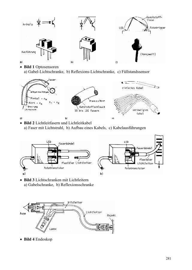
17.3 Lichtschranken und Lichtleiter Lichtschranken gehören zur Gruppe der Optosensoren, die unter Ausnutzung optischer Effekte die Erfassung und Messung mechanischer Größen gestatten. Bild 1 zeigt nebeneinander Prinzip und Ausführungsbeispiele zur Gabelschranke, zum Reflexionstaster und zu dem noch relativ jungen Füllstandssensor. Sie alle sind Anordnungen mit einem Lichtsender (z.B. LED) und einem Lichtempfänger (z.B. Fototransistor oder Fototrigger) in optischer Kopplung und können daher auch als Optokoppler aufgefasst werden. Die Schaltungstechnik ist entsprechend. Im Gegensatz zum normalen Optokoppler wird hier eine Steuerwirkung nicht über die LED, sondern durch eine Änderung in der Lichtübertragung vorgenommen. Bei der Gabelschranke geschieht dies durch mechanische Unterbrechung des Lichtstrahls und beim Reflexionstaster durch Änderung der Reflexion auf einer benachbarten Fläche. Wie beim normalen Optokoppler verwendet man praktisch ausschließlich infrarot strahlende GaAs-LEDs, die mit ihrem Strahlungsspektrum gut an die spektrale Empfindlichkeit moderner Si-Fototransistoren angepasst sind. Beim Reflexionstaster setzt man häufig Darlingtonausführungen ein, weil diese wegen der doppelten Stromverstärkung mit weniger Licht zur Durchsteuerung auskommen. Üblicherweise sind LED und Fototransistor an der Lichtdurchgangs-stelle mit einer Linse versehen, so dass in vielen Fällen eine zusätzliche Optik entbehrlich ist. Besonders interessant ist der an dritter Stelle gezeigte Füllstandssensor. Eine LED und ein Fototrigger sind an der Grundfläche einer klaren Kunststoffhalbkugel so eingegossen, dass das Licht normaler-weise von der Außenfläche der Halbkugel nach innen auf den Fototrigger totalreflektiert wird. Wird die Halbkugel von einer Flüssigkeit benetzt, so ändert sich der Brechungsindex an der Grenzfläche, und das Licht kann in die Flüssigkeit austreten. Der Fototrigger wird dunkel. Die Kunststoffhalbkugel stellt im Grunde einen Lichtleiter dar mit der Fähigkeit, Lichtstrahlen in einer bestimmten Weise zu führen. Für allgemeine Anwendungen der Lichtleitung werden wegen ihrer Flexibilität hauptsächlich dünne Glas- oder Kunststofffasern verwendet. Bild 2a zeigt die Lichtführung in einer einzelnen Faser. Lichtstrahlen, die innerhalb eines bestimmten Öffnungswinkels auf der Stirnseite eintreten, werden an der Grenzschicht zwischen dem Kern und einem Mantel mit kleinerer Brechzahl n totalreflektiert und treten über einen Zickzack-Weg am anderen Faserende wieder aus. Dabei tritt eine gewisse Dämpfung auf, die von der Wellenlänge des Lichtes abhängig ist, außerdem auch vom Material. Glas ist lichtdurchlässiger als Kunststoff. Den Anwendungsbereich der Lichtleitung mit Glas- oder Kunststofffasern bezeichnet man als Faseroptik (fibre optics). Bild 2b zeigt den Aufbau eines Lichtleitkabels, wie er mit Glasfasern üblich ist. Die Faserenden werden verklebt und poliert und im Übrigen dann nach Bild 2c mit Endhülsen eingefasst. Durch Aufspaltung des Faserbündels auf mehrere Teilbündel sind mehrarmige Lichtleiter herstellbar. Man kann auch Querschnittswandlungen vornehmen, beispielsweise zum Übergang von einem runden auf einen eckigen Querschnitt. Bild 3 zeigt Anwendungsbeispiele, bei denen solche Möglichkeiten vorteilhaft genutzt werden können. Die gezeigten Lichtschranken mit Lichtleitern ermöglichen eine Signalaufnahme an schwer zugänglichen und von der Elektronik entfernten Objekten. Ist das Faserbündel an der Eintritts- und Austrittsfläche in fester und gleicher Ordnung zusammen-gesetzt, so spricht man von einem kohärenten Bündel oder auch Bildleiter. Jeder von der Ein-trittsfläche aufgenommene Lichtstrahl tritt an der gleichen Stelle auf der anderen Seite wieder aus. Mit einem Lichtleiter dieser Art lassen sich demnach Bilder übertragen, wobei das Auflösungs-vermögen umso besser wird, je kleiner der Faserdurchmesser ist. Für Bildleiter werden daher besonders dünne Fasern verwendet, teilweise mit Durchmessern unter 20 µm. Ihre hauptsächliche Anwendung liegt in der Endoskopie, im Bereich der medizinischen und technischen Diagnostik (Bild 4). Bildleiter werden auch in starrer Form hergestellt, indem man beim Herstellungsprozess die Außen-haut der Fasern miteinander verschmilzt. Das hat den Vorteil, dass der ungenutzte Zwischenraum zwischen den einzelnen Fasern verringert wird und ein gutes Auflösungsvermögen erzielt wird. Ein sehr dickes aber kurzes Bündel dieser Art bildet eine Faserplatte, deren Stirnflächen plan oder aus besonderen Gründen auch konkav oder konvex geschliffen werden können. Durch eine plan-konkave Platte lässt sich ein gekrümmtes Bild ebnen, beispielsweise das Oszillogramm auf einem nichtebenen Schirm eines Oszilloskops. Bei mehrstufigen Bildverstärkern werden Faserplatten auch als Fenster-und Koppelelemente eingesetzt (siehe Abschnitt 8.5).
Literatur: [17–3], [17–4]
281
Bild 1 Optosensorena) Gabel-Lichtschranke, b) Reflexions-Lichtschranke, c) Füllstandssensor
Bild 2 Lichtleitfasern und Lichtleitkabel a) Faser mit Lichtstrahl, b) Aufbau eines Kabels, c) Kabelausführungen
Bild 3 Lichtschranken mit Lichtleitern a) Gabelschranke, b) Reflexionsschranke
Bild 4 Endoskop

282
17.4 Optische Nachrichtentechnik Lichtleiter werden heute oft anstelle von Kupferleitungen zur Signalübertragung über kürzere und längere Wege eingesetzt. Vorteilhaft ist dabei immer die Potentialtrennung zwischen Sender und Empfänger sowie die Unempfindlichkeit gegenüber elektromagnetischen Störfeldern. Da zumindest bei größeren Entfernungen die Wellennatur des Lichtes eine Rolle spielt, hat sich für die nachrichtentechnische Anwendung die Bezeichnung Lichtwellenleiter (LWL) eingeführt. In der Regel wird für einen Nachrichtenkanal nur ein einfasriges Lichtleitkabel verwendet (Bild 1).Bei kurzen Entfernungen unter 50 m genügen Kunststoffleiter, die mit einem scharfen Messer auf Maß geschnitten und über Steckverbindungen leicht an ein Sende- und Empfangselement angekoppelt werden.Mehrfasrige Kabel haben den Vorteil, dass man Signale auf mehrere Wege verteilen kann. Dazu legt man Verzweigungsstellen an entsprechend Bild 1b. Die Schaltungstechnik auf der elektrischen Seite unterscheidet sich prinzipiell nicht von derjenigen bei Optokopplern. Um bei Glasfasern ausreichende Flexibilität zu gewährleisten, sind Durchmesser unter 200 µm erforderlich. Für die Bearbeitung sind besondere Werkzeuge nötig, und beim Aufbau von Steckverbindungen ist höchste Präzision erforderlich. Aufgrund der besseren Lichtdurchlässigkeit kommt aber für größere Entfernungen nur die Glasfaser als Übertragungsmedium in Frage. Bild 2macht den Unterschied zur Plastikfaser durch einen Vergleich der Dämpfungswerte deutlich, die stark vom Material und der Wellenlänge des Lichtes abhängen. Nutzt man bei einer hochwertigen Glasfaser das „Übertragungsfenster“ 1 oder 2 im nahen Infrarotbereich, so erhält man eine Dämpfung um 1 dB/km. Im dritten Fenster kommt man sogar auf Werte von 0,2 dB/km herunter. Demgegenüber betragen derzeit die günstigsten Werte für die Plastikfaser etwa 150 dB/km, wenn man mit sichtbarem Licht im grün/gelben Bereich arbeitet. Auf einer Strecke von 20 m ergibt sich damit bereits eine Dämpfung von 3 dB, d.h. ein Lichtverlust von 50 %. Hinzu kommen weitere Verluste an den Steckverbindungen. Bild 3 macht deutlich, dass die optische Nachrichtentechnik im elektromagnetischen Spektrum nur einen relativ schmalen Frequenzbereich zwischen 1014 Hz und 1015 Hz nutzt. Angesichts der hohen Absolutwerte der Frequenz ist die entsprechende Bandbreite f jedoch außerordentlich groß, verglichen mit üblichen Werten in der konventionellen Nachrichtentechnik. Für die Weitverkehrs-technik stehen auch geeignete Sende- und Empfangselemente bereit, mit denen man in den verschiedenen Übertragungsfenstern optimal arbeiten kann. Auf der Sendeseite handelt es sich dabei um spezielle lichtstarke LEDs und Laserdioden (LDs). Die Letzteren besitzen wie die LED eine pn-Struktur, wobei aber in komplizierter Weise ein innerer Resonanz- und Verstärkungseffekt ausgenutzt wird. Im Gegensatz zur LED tritt dabei das Licht in scharf gebündelter Form und im Wesentlichen monochromatisch an der Stirnseite des Halbleiterplättchens aus. Auf der Empfangsseite sind es PIN-Dioden und sog. Avalanche-Fotodioden (APDs). Die Ersteren zeichnen sich durch eine geringe Sperrschichtkapazität aus, wodurch kurze Schaltzeiten möglich werden1). Die Letzteren nutzen den Lawinen-Effekt (Avalanche-Effekt), wie er von der Z-Diode her bekannt ist, zur Verstärkung der Empfangssignale.
Beim Lichtleiter selbst unterscheidet man neben der Materialart – Glas oder Plastik – sein Profil. Darunter versteht man nach Bild 4 den Verlauf des Brechungsindex n über dem Radius r. Bei einer „Stufenindexfaser“ ändert sich dieser sprunghaft zwischen Kern und Mantel. In einer derartigen Faser mit relativ dickem Kern kommen aufgrund unterschiedlicher Ausbreitungswege (Zickzack-Wege bzw. „Wellenmoden“) gleichzeitig eingekoppelte Wellenzüge des Lichtes mit einer gewissen Zeitdifferenz am Ende der Faser an. Das bedeutet, dass ein schmaler Lichtimpuls am Ausgang verbreitert erscheint und dicht aufeinander folgende Impulse sogar ineinander fließen können. Diese als Dispersion bezeichnete Erscheinung nimmt mit der Leitungslänge zu und begrenzt die Anwendbarkeit nach hohen Frequenzen hin. Ein wirksames Gegenmittel ist die drastische Verringerung des Kerns bis auf einen Durchmesser unter 10 µm. Aus der „Multimodefaser“ wird dann eine „Monomodefaser“ mit nur einer Ausbreitungs-richtung ohne Dispersion. In der Weitverkehrstechnik hat sich diese heute weitgehend durchgesetzt gegenüber der „Gradientenfaser“, die dort bisher dominierte. In dieser läuft das Licht auf gekrümmten Bahnen. Auf der äußeren (längeren) Bahn im optisch dünneren Medium benötigt es etwa die gleiche Zeit wie auf der mittleren (kürzeren) Bahn durch das optisch dichtere Medium. Damit bleibt die Dispersion auch hier relativ gering.
1) Siehe auch Abschnitt 17.2. Literatur: [17–5], [17–6], [17–7], [17–8]

283
Bild 1 Optische Übertragungsstrecke und Verbindungselemente*)
a) einfasriges System, b) mehrfasriges System
Bild 2 Typischer Dämpfungsverlauf Bild 3 Elektromagnetisches Strahlungsspektrum
Multimodefaser mit Stufenprofil (Stufenindexfaser)
Monomodefaser mit Stufenprofil (Stufenindexfaser)
Multimodefaser mit Gradientenprofil (Gradientenindexfaser)
Bild 4 Aufbau und Merkmale verschiedener Fasertypen (Maße in m, Klammerwerte gelten für Kunststofffaser)
*) Steckverbinder mit Kunststoffleitern sind relativ unproblematisch. Der Lichtleiter wird samt Schutzmantel in eine Auf-
nahmebuchse eingeführt und festgeschraubt.
106
8.6 Flüssigkristall-Anzeigen (LC-Displays) LC-Display (Liquid Crystal Display) ist die englische Bezeichnung für Flüssigkristall-Anzeige auf der Basis der Flüssigkristallzelle nach Bild 1a. Diese stellt im Grunde einen ebenen Plattenkondensator dar mit einer „nematischen“ Flüssigkeit als Dielektrikum und transparenten Zinn-Oxidschichten auf Glas als Beläge. Nematisch nennt man einen Flüssigkeitszustand, in dem die Moleküle eine bestimmte Ausrichtung besitzen, die unter dem Einfluss eines elektrischen Feldes veränderbar ist. Damit ändert sich auch die Lichtdurchlässigkeit, was bei einer segmentweisen Unterteilung einer der beiden Elektroden zur Darstellung von Ziffern und Zeichen genutzt werden kann.Bild 1b zeigt eine derartige Anordnung mit der Zeichendarstellung auf dem Grundglas, während die gemeinsame Gegenelektrode dem Betrachter zugewandt ist. Von der Frontseite her einfallendes Licht kann den Kristall durchdringen und wird von der auf der Rückseite angebrachten Reflektorfolie zurückgestrahlt, so dass die Flüssigkeit hell erscheint. Legt man eine Spannung an zwischen einem oder mehreren Segmenten und der gemeinsamen Gegenelektrode, so wird in diesem Bereich der Flüssig-kristall lichtundurchlässig und erscheint daher dunkel. Die eben beschriebene „reflektive“ Betriebsweise setzt eine Lichteinstrahlung von der Frontseite her voraus. Möglich ist auch ein „transmissiver“ Betrieb mit rückseitiger Beleuchtung. Mit einer halbdurchlässigen Reflektorfolie kann man beide Betriebsweisen kombinieren (transflektiver Be-trieb), beispielsweise in Verbindung mit einer geeigneten Hintergrundbeleuchtung, um die Lesbarkeit bei schwachem Tageslicht sicherzustellen1). Fremdlicht ist immer erforderlich, da der Flüssigkristall selbst kein Licht erzeugt. Es handelt sich um eine passive Anzeigeform. Bild 1c zeigt die Ausführung einer mehrstelligen Sieben-Segment-Anzeige. In der Regel wird heute die Segmentierung auf dem Frontglas vorgenommen, während die gemein-same Gegenelektrode als sog. Backplane (BP) sich auf dem Grundglas befindet. Der grundsätzliche Wirkungsmechanismus ändert sich dadurch jedoch nicht. Bild 2a zeigt zu diesem Fall die physikali-schen Vorgänge mehr im Detail mit einem Blick in das aufgeklappte Display. Bei der üblichen „Drehzelle“(TN-Zelle, Twisted Nematic-Cell) ist der Kristall (links) um 90° in sich verdreht. Über eine Polarisationsfolie (unten) eintretendes polarisiertes Licht wird in der Zelle ebenfalls um 90° gedreht, so dass es einen quer gestellten Polarisator auf der Gegenseite durchdringen kann. Hebt man die Moleküldrehung durch Anlegen einer elektrischen Spannung auf (rechts), so wird der Lichtdurchgang unterbunden. Das entspricht der bereits oben beschriebenen Funktion. Zum Ansteuern einer LC-Zelle genügt eine Spannung von wenigen Volt (2 V bis 5 V) bei einer Stromaufnahme in der Größenordnung Mikroampere. Wegen der Gefahr einer elektrolytischen Zersetzung ist Dauerbetrieb nur mit Wechselspannung zulässig (vorzugsweise rechteckförmig mit 100 Hz). Die Ansteuerung geschieht üblicherweise nach der Methode der Phasenumschaltung mit speziellen Ansteuerbausteinen nach Bild 2b. Gleichphasige Potentialbewegung z.B. am Segment f und der Gegenelektrode (BP) ergibt keine Spannung UFB. Der Kristall ist an der betreffenden Stelle also lichtdurchlässig. Bei gegenphasiger Potentialbewegung am Segment e entsteht eine rechteckförmige Wechselspannung UEB. Dort sperrt die Zelle und das Segment erscheint dunkel. Das Umschalten geschieht jeweils mit einer gewissen Trägheit, wie Bild 2c für das beliebige Segment x zeigt. Die oben beschriebene direkte (oder statische) Ansteuerung ist praktisch nur durchführbar bei einer überschaubaren Anzahl von Segmenten. Bei vielstelligen Anzeigen geht man über zur Multiplexsteuerung, auch dynamische Steuerung genannt1). Bild 3a zeigt wieder das Prinzip am Beispiel der Sieben-Segment-Anzeige mit Dezimalpunkt. Die „Backplane“ ist dreifach unterteilt mit den Anschlüssen B1, B2 und B3. Die Segmente werden gruppenweise an die Leitungen S1, S2 und S3 geschaltet. Das Segment e erreicht man also jetzt über die Leitungen B2 und S1. Es wird im Beispiel nur während eines Drittels der Periode T eingeschaltet, wenn die Spaltenleitung S1 jeweils das entgegengesetzte Potential (negativ) zur Reihenleitung B2 (positiv) erhält. So kommt man mit 6 Leitungen aus anstelle von 9 bei direkter Ansteuerung. Besonders drastisch ist die Leitungsersparnis bei Punkt-Matrix-Anzeigen mit sehr vielen Segmenten, hier Dot oder Pixel (picture element) genannt. Für 20000 Pixel genügen 100 Reihen- und 200 Spaltenleitungen im Gegensatz zu 20001 Leitungen bei direkter Steuerung. Um den Faktor 10 höher noch liegen die Zahlen beim LC-Bildschirm, wo heute Aktiv-Matrix-Steuerung angewendet wird (Bild 3c). Dabei werden die einzelnen Pixel über integrierte MOS-Transistoren, sog. Dünnfilm-Transistoren angesteuert.
1) Siehe dazu auch Abschnitt 3.6. Literatur: [8–9], [8–10], [8–11], [8–12], [8–13]

107
Bild 1 Flüssigkristallanzeige (Grundlagen) a) Flüsssigkristallzelle, b) Aufbau eines Displays, c) 7-Segment-Display
Bild 2 Feldeffekt-Drehzellen (TN-Zellen)*)
a) Aufbau und Wirkungsweise**), b) direkte Ansteuerung, c) Schaltverhalten
Bild 3 Multiplexsteuerung (Matrixsteuerung, dynamische Steuerung) a) Grundschema, b) Matrixersatzbild, c) aktive Matrix (TFT-LCD) ***)
*) Erfunden von Schadt und Helfrich (1971). **) Darstellung der „positiven“ Betriebsweise (Positiv-Mode). Durch eine Parallelausrichtung der Polarisatoren lässt
sich die Schalterfunktion umkehren: Lichtdurchlass mit Spannung, Lichtsperre ohne Spannung (negative Betriebsweise, Negativ-Mode).
***) Großflächig ausgebildete LCDs mit Aktiv-Matrix-Steuerung bilden die Grundlage moderner Fernsehbildschirme. Diese verdrängen mehr und mehr die Bildröhren und behaupten sich auch gegenüber konkurrierenden Plasma-Bildschirmen, bei denen die Pixel durch winzige Gasentladungen gebildet werden.