electronics lab-332 semester 4 - madinpoly.com lab mnl 332.pdf · electronics lab-332 semester 4...
TRANSCRIPT

ELECTRONICS LAB-332
SEMESTER 4
CHARACTERISTICS OF P-N JUNCTION DIODE
AIM
To determine the forward characteristics of a p-n junction diode and determine the static and dynamic
resistance.
COMPONENTS AND EQUIPMENTS REQUIRED
SI
No
NAME SPECIFICATION QUANTITY
1
2
3
4
5
6
7
8
POWER SUPPLY
VOLTMETER
AMMETER
DIODE
RESISTOR
POTENTIOMETER
BREAD BOARD
CONNECTING WIRES
0-30V
0-20V
0-100 mA
IN 4001-Si OR
OA 79-Ge
1KΩ
1KΩ
1 NO
1 NO
1 NO
1 NO
1 NO
1 NO
1NO
AS REQUIRED
THEORY
When a P type and N type semiconductors are joined together, a junction diode is created .It has a unique
ability to permit current only in one direction. The lead connected to P type is called anode and the lead
connected to N type is called cathode.If the anode of the diode is connected to the +ve terminal of a
battery and cathode to the –ve terminal,the set up is called forward bias.the diode does not pass any
current till the battery voltage exceeds the potential barrier( o.7 V for Si & 0.3 V for Ge). Once the battery
potential exceeds the barrier potential high forward current in the order of mA flows through the diode
due to the movements of hole and electrons.
The static resistance or DC resistance is the ratio of DC voltage across the diode to the
DC current flows through it. Dynamic resistance or AC resistance of the diode at any point is the
reciprocal of the slope of the charaecteristic at that point.
ie dynamic resistance= change in voltage/ change in current = ΔV/ΔI
PROCEDURE
1. Set up the circuits as shown in figure on bread board.
2. Switch on the power supply
3. Varying the voltage across the diode in steps and find corresponding current.

4. Repeat the above steps for different values of voltage
TABULATION:
RESULT
Plotted the forward characteristics of PN junction Si diode and its
Static resistance =…………….
Dynamic resistance =………….
mA
V
R1
1k
0-30 V
1K POT
+
+
_
_
1N4001
0-1V
0-50mA
V in volt I in mA
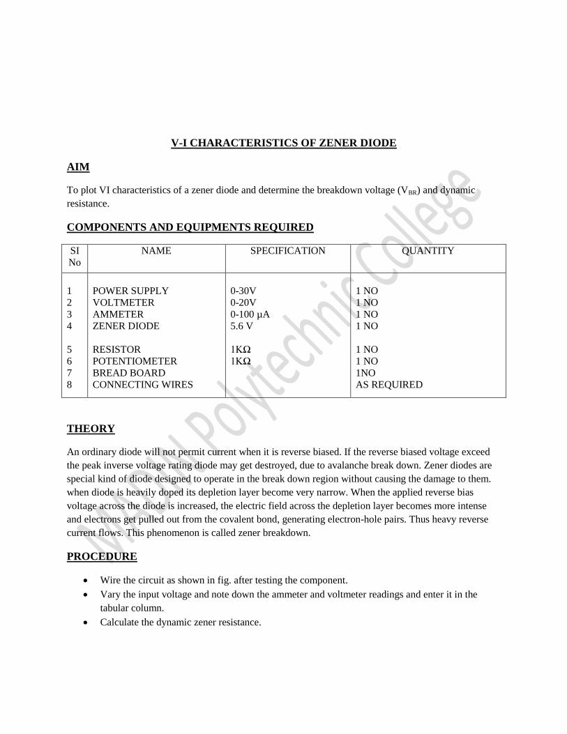
V-I CHARACTERISTICS OF ZENER DIODE
AIM
To plot VI characteristics of a zener diode and determine the breakdown voltage (VBR) and dynamic
resistance.
COMPONENTS AND EQUIPMENTS REQUIRED
SI
No
NAME SPECIFICATION QUANTITY
1
2
3
4
5
6
7
8
POWER SUPPLY
VOLTMETER
AMMETER
ZENER DIODE
RESISTOR
POTENTIOMETER
BREAD BOARD
CONNECTING WIRES
0-30V
0-20V
0-100 µA
5.6 V
1KΩ
1KΩ
1 NO
1 NO
1 NO
1 NO
1 NO
1 NO
1NO
AS REQUIRED
THEORY
An ordinary diode will not permit current when it is reverse biased. If the reverse biased voltage exceed
the peak inverse voltage rating diode may get destroyed, due to avalanche break down. Zener diodes are
special kind of diode designed to operate in the break down region without causing the damage to them.
when diode is heavily doped its depletion layer become very narrow. When the applied reverse bias
voltage across the diode is increased, the electric field across the depletion layer becomes more intense
and electrons get pulled out from the covalent bond, generating electron-hole pairs. Thus heavy reverse
current flows. This phenomenon is called zener breakdown.
PROCEDURE
Wire the circuit as shown in fig. after testing the component.
Vary the input voltage and note down the ammeter and voltmeter readings and enter it in the
tabular column.
Calculate the dynamic zener resistance.

TABULATION
V in volt I in mA
RESULT
Plotted the VI characteristics of Zener diode and its
Break down voltage (VBR) = …………….
Dynamic resistance = ………….
mA
V
R1
1k
0-30 V
1K POT
+
+
_
_
0-20 V
0-100mA
SZ5.6
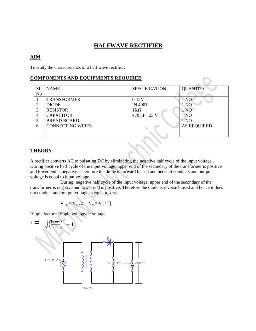
HALFWAVE RECTIFIER
AIM
To study the characteristics of a half wave rectifier.
COMPONENTS AND EQUIPMENTS REQUIRED
SI
No
NAME SPECIFICATION QUANTITY
1
2
3
4
5
6
TRANSFORMER
DIODE
RESISTOR
CAPACITOR
BREAD BOARD
CONNECTING WIRES
0-12V
IN 4001
1KΩ
470 μF , 25 V
1 NO
1 NO
1 NO
1 NO
1 NO
AS REQUIRED
THEORY
A rectifier converts AC to pulsating DC by eliminating the negative half cycle of the input voltage .
During positive half cycle of the input voltage, upper end of the secondary of the transformer is positive
and lower end is negative. Therefore the diode is forward biased and hence it conducts and out put
voltage is equal to input voltage.
During negative half cycle of the input voltage, upper end of the secondary of the
transformer is negative and lower end is positive. Therefore the diode is reverse biased and hence it does
not conduct and out put voltage is equal to zero.
Vrms = Vm /2 Vdc= Vm / ∏
Ripple factor= Ripple voltage/dc voltage
ᵞ = 𝑉𝑟𝑚𝑠
𝑉𝑑𝑐 2
− 1
1k0-230V/50Hz
230V/9V
D
470 microF OUTPUT

PROCEDURE
1. Set up the circuits on bread board
2.Observe wave form across RL on the CRO.
3.Note the peak value
4.Calculate the ripple factor and Vdc using the equations.
5.Repeat the same procedure with filter circuit.
RESULT
Studied the characteristics of half wave rectifier.
Theoretical value of ripple factor =………...
Practical value of ripple factor =……………
Difference between Theoretical value and Practical value =………...

CENTRE TAPPED RECTIFIER
AIM
To study the characteristics of a centre tapped rectifier.
COMPONENTS AND EQUIPMENTS REQUIRED
SI
No
NAME SPECIFICATION QUANTITY
1
2
3
4
5
6
TRANSFORMER
DIODE
RESISTOR
CAPACITOR
BREAD BOARD
CONNECTING WIRES
9-0-9V
1N 4001
1KΩ
470 μF , 25 V
1 NO
2 NO
1 NO
1 NO
1 NO
AS REQUIRED
THEORY
A rectifier converts AC to pulsating DC.During positive half cycle of the input voltage, upper end of the
secondary of the transformer is positive and lower end is negative. Therefore the diode D1 is forward
biased and diode D2 is reverse biased .Therefore D1 conducts and out put voltage is equal to input voltage.
During negative half cycle of the input voltage, upper end of the secondary of the
transformer is negative and lower end is positive. Therefore the diode D1 is reverse biased and diode D2
forward biased, hence it conducts and output voltage is same as that of positive half cycle.
Vrms = Vm / 2 Vdc=2 Vm / ∏
Ripple factor = Ripple voltage/dc voltage
ᵞ = 𝑉𝑟𝑚𝑠
𝑉𝑑𝑐 2
− 1
230V/50Hz
470 microF
D1
D2
9-0-9
1K

PROCEDURE
1. Set up the circuits on bread board
2. Observe the transformer secondary voltage(Vac) and wave form across RL on the CRO.
3. Note the peak value
4. Calculate the ripple factor and Vdc using the equations.
5. Repeat the same procedure with filter circuit.
RESULT
Studied the characteristics of centre tapped rectifier.
Theoretical value of ripple factor =………...
Practical value of ripple factor =……………
Difference between Theoretical value and Practical value =………...

BRIDGE RECTIFIER
AIM
To study the characteristics of a centre tapped rectifier.
COMPONENTS AND EQUIPMENTS REQUIRED
SI
No
NAME SPECIFICATION QUANTITY
1
2
3
4
5
6
TRANSFORMER
DIODE
RESISTOR
CAPACITOR
BREAD BOARD
CONNECTING WIRES
0-12V
IN 4001
1KΩ
470 μF , 25 V
1 NO
4 NO
1 NO
1 NO
1 NO
AS REQUIRED
THEORY
A rectifier converts AC to pulsating DC.During positive half cycle of the input voltage, upper end of the
secondary of the transformer is positive and lower end is negative. Therefore the diode D1 and D3 are
forward biased and diode D2 and D4 are reverse biased .Therefore diode D1 and D3 conducts and out put
voltage is equal to the input voltage.
During negative half cycle of the input voltage, upper end of the secondary of the
transformer is negative and lower end is positive. Therefore the diode D1 and D3 are reverse biased and
diode D2 and D4 are forward biased, hence it conducts and out put voltage is same as that of positive half
cycle.
Vrms = Vm / 2 Vdc=2 Vm / ∏
Ripple factor= Ripple voltage/dc voltage
ᵞ = 𝑉𝑟𝑚𝑠
𝑉𝑑𝑐 2
− 1

PROCEDURE
1. Set up the circuits on bread board
2. Observe the transformer secondary voltage(Vac) and wave form across RL on the CRO.
3. Note the peak value
4. Calculate the ripple factor and Vdc using the equations.
5. Repeat the same procedure with filter circuit.
RESULT
Studied the characteristics of bridge rectifier.
Theoretical value of ripple factor =………...
Practical value of ripple factor =……………
Difference between Theoretical value and Practical value =………...
~
~
+-230V/50Hz
470 microF
D1
D2
9-0-9
1KD3
D4

COMMON EMITTER TRANSISTOR CHARACTERISTICS
AIM
To plot the VI characteristics of common emitter configuration of a given transistor and plot the DC load
line.
COMPONENTS AND EQUIPMENTS REQUIRED
SI
No
NAME SPECIFICATION QUANTITY
1
2
3
4
5
6
7
8
POWER SUPPLY
VOLTMETER
AMMETER
TRANSISTOR
RESISTOR
POTENTIOMETER
BREAD BOARD
CONNECTING WIRES
0-30 V
0-10V, 0-30V
0-100 mA, 0-100 μA
BC 107
1.5 KΩ
1 KΩ
2 NOS
1 EACH
1 EACH
1 NO
1 NO
2 NOS
1 NO
AS REQUIRED
THEORY A transistor is a 3 terminal active device. The 3 terminals are emitter(E),base(B)and collector(C).In
CE configuration we make the emitter common to both input and output for normal operation.The base-
emitter junction is forward biased and collector-emitter junction is reverse biased.
The input characteristics is plotted between input current(IB) and the input voltage(VBE) with keeping
output voltage (VCE) constant. The input dynamic resistance ri is calculated using the equation
ri= ΔVBE/ΔIB , keeping VCE is constant.
The output characteristics is plotted between output current(IC) and the output voltage(VCE) with
keeping input current (IB)constant.
The output dynamic resistance r0 is calculated using the equation
ro= ΔVCE/ΔIC , keeping IB is constant.
PROCEDURE
For input characteristics
1. Check the transistor using multimeter. Switch on the power supply keeping rheostat at minimum
position. Switch off the collector to emitter power supply.
2. Note down the base current for different values of VBE.
3. Repeat the step 2 for different values of VCE , say 3V, 6V.
4. Draw the characteristics on a graph sheet and calculate dynamic input resistance.
For out put characteristics
1. Check the transistor using multimeter. Switch on the power supply keeping rheostat at minimum
position. Switch off the base to emitter power supply.
2. Note down the collector current for different values of VCE.
3. Repeat the step 2 for different values of base current , say 80μA, 100μA.
4. Draw the characteristics on a graph sheet and calculate dynamic out put resistance.

TABULATION
Input charecteristics Out put charecteristics
IB = 60μA IB = 80μA IB = 100μA IC VCE. IC VCE. IC VCE.
RESULT
Plotted the input and out put charecteristics of a CE transistor.
Dynamic input resistance = ……………
Dynamic out put resistance = ………….
1
23
mA
uA
V
V0-5V
1K POT
47K
0-100microA
BC 107
VBE
0-1V
0-100mA
0-30V
0-30V
1K POT
1K
+
+
+
+_
_
_
_
IB
IC
VCE
VCE = 0V VCE = 3V VCE = 6V IB VBE. IB VBE. IB VBE.

RC PHASE SHIFT OSCILLATOR
AIM
To set up an RC phase shift oscillator and to observe the sinusoidal output waveform.
COMPONENTS AND EQUIPMENTS REQUIRED
SI
No
NAME SPECIFICATION QUANTITY
1
2
3
4
5
6
POWER SUPPLY
TRANSISTOR
RESISTORS
CAPACITORS
BREAD BOARD
CONNECTING WIRES
12 V
BC 107
4.7 KΩ
10 K, 2.2K, 47K, 680Ω
0.01μF
22μF , 1μF
1 NO
1 NO
3 NOS
1 EACH
3 NOS
1 EACH
1 NO
AS REQUIRED
THEORY
An oscillator is an electronic circuit for generating an ac signal voltage with a dc supply as the only input
requirement. The frequency of the generated signal is decided by circuit constants. An oscillator requires
an amplifier and a positive feed back from out put to input. The barkhausen criterian for sustained
oscillation is (1) loop gain=1 ie Aβ =1 , where A is the gain and β is the feed back factor
(2) Total phase shift =00 or 360
0
A CE amplifier introduces a 1800 phase shift and feed back network another 180
0. Feed back
network consist of 3 RC network each produces a 600 and hence total 180
0.
Frequency of oscillation f = 1/ 2∏RC√6

PROCEDURE
1. Set up the amplifier part of the oscillator and test the dc conditions.
2. Connect the feedback network and observe the sine wave on CRO and measure its amplitude and
frequency.
RESULT
Observed the sinusoidal wave form at the out put of oscillator.
VCC_ARROW
1
23
4.7K 4.7K
4.7K
0.01mF 0.01mF0.01mF
1mF
22mF10K
2.2K47K
680 OHM
BC 107
Vcc +12V
V0

ASTABLE MULTIVIBRATOR
AIM
To set up an astable mulitivibrator using transistors, study its performance and observe the wave form at
various points.
COMPONENTS AND EQUIPMENTS REQUIRED
SI
No
NAME SPECIFICATION QUANTITY
1
2
3
4
5
6
7
POWER SUPPLY
TRANSISTOR
RESISTORS
CAPACITORS
LED
BREAD BOARD
CONNECTING WIRES
6 V
BC 548
10 KΩ
1KΩ
100μF
GREEN, RED
1 NO
2 NOS
2 NOS
2 NOS
2 NOS
1 EACH
1 NO
AS REQUIRED
THEORY
Astable multivibrator is also called free running oscillator. It does not have a stable state. This circuit
transist from one quasi stable state to the other and back automatically depending upon the charging and
discharging time of two capacitors.
When one transistor is in ON state other remains in OFF state. The collector voltage of the on
transistor is approximately 0.3 V and that of OFF transistor is VCC. Suppose transistor Q1 is OFF and Q2 is
ON

PROCEDURE
1. Verify the condition of all components.
2. Set up the circuit and observe the collector and base waveforms of both the transistors.
RESULT
Observed the collector and base waveforms of both the transistors.
1
23
1
23
LEDLED
IKIK 10K 10K
BC 548
BC 548
100microF 100microF
Vcc=+6V
Q1 Q2
C2C1
R1 R2
RC2RC1