electroabsorption spectroscopy — direct determination of the strong piezoelectric field in...
TRANSCRIPT
Electroabsorption Spectroscopy ––Direct Determination of the Strong Piezoelectric Fieldin InGaN/GaN Heterostructure Diodes
P. Kiesel1) (a), F. Renner (a), M. Kneissl (b), N. M. Johnson (b), and
G. H. Dohler (a)
(a) Institute for Technical Physics I, Friedrich-Alexander University Erlangen-Nurnberg,Erwin-Rommel-Str. 1, D-91058 Erlangen, Germany
(b) Xerox Palo Alto Research Center, Palo Alto, CA, USA
(Received July 2, 2001; accepted August 14, 2001)
Subject classification: 77.65.–j; 78.20.Ci; 78.66.Fd; S7.14
We report on room temperature electroabsorption measurements on (In)GaN heterostructure p–i–ndiodes. This technique allows a precise determination of the strong changes of internal fields at theInGaN/GaN hetero interface due to differences in the spontaneous polarisation and strain-inducedpiezoelectric fields. The measured fields vary between 1 and 1.4 MV/cm for thin InGaN layers withan In content ranging from approximately 7% to 9%. Absorption spectroscopy is also well suited toinvestigate the optical properties of GaN layers. In contrast to Si-doped or intrinsic materialMg-doped GaN films reveal a pronounced absorption tail below the band edge with absorption coef-ficients of about 30 cm––1 at typical emission wavelengths (l � 400 nm) of InGaN laser diodes.
Introduction The GaN material system has proven to be an excellent material foropto-electronic components in the near-ultraviolet and visible spectral range as well asfor high temperature and high speed electronics [1]. Although there are already com-mercial devices available there is still a considerable lack of understanding regardingfundamental material issues.
Electroabsorption spectroscopy is a powerful and sensitive technique to obtain de-tailed information about optical properties and the electronic band structure of semi-conductors. Surprisingly, only a few studies have been performed so far on group-IIInitride-based semiconductor films, although many optical properties in these films haveyet to be accurately determined. For example, in wurtzite InGaN/GaN heterostructures,large internal fields exist due to strain-induced piezoelectric fields and differences in thespontaneous polarisation [2, 3]. These internal fields have been discussed in many theo-retical and experimental publications but reliable values for these fields are still lackingand their impact on light emitting devices is still debated. In this paper, we will showthat electroabsorption spectroscopy on GaN heterostructure p–i–n diodes with thinInGaN layers in the intrinsic region provide an excellent method for determining accu-rate values for the internal field. The principle idea of this method is to compensate thestrong internal fields in the InGaN layer by applying a p–n voltage.
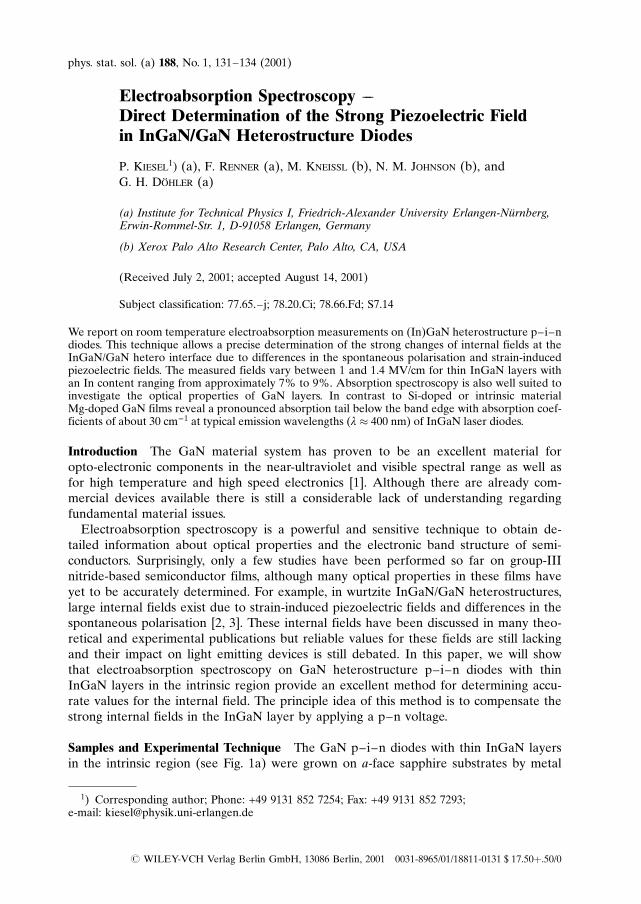
Samples and Experimental Technique The GaN p–i–n diodes with thin InGaN layersin the intrinsic region (see Fig. 1a) were grown on a-face sapphire substrates by metal
1) Corresponding author; Phone: +49 9131 852 7254; Fax: +49 9131 852 7293;e-mail: [email protected]
phys. stat. sol. (a) 188, No. 1, 131–134 (2001)
# WILEY-VCH Verlag Berlin GmbH, 13086 Berlin, 2001 0031-8965/01/18811-0131 $ 17.50þ.50/0
organic chemical vapour deposition (MOCVD). Figure 1b shows the calculated banddiagram of such a heterostructure diode at zero bias assuming no field and a highpiezoelectric field of 1.5 MV/cm in the InGaN layer, respectively.
By applying a p–n voltage U to the heterostructure diodes we are able to control theelectric fields within the intrinsic region of the p–i–n diode. This leads to field-inducedabsorption changes for photon energies around the band gap of the semiconductormaterials within the intrinsic region. Since the thin InGaN layer and the surroundingGaN are exhibiting different band gap energies, the electroabsorption in both materialscan be observed separately. The field-induced absorption changes can be resolved veryprecisely by measuring the transmitted light for various applied voltages. These investi-gations can be performed at room temperature even with diodes containing only asingle narrow quantum well.
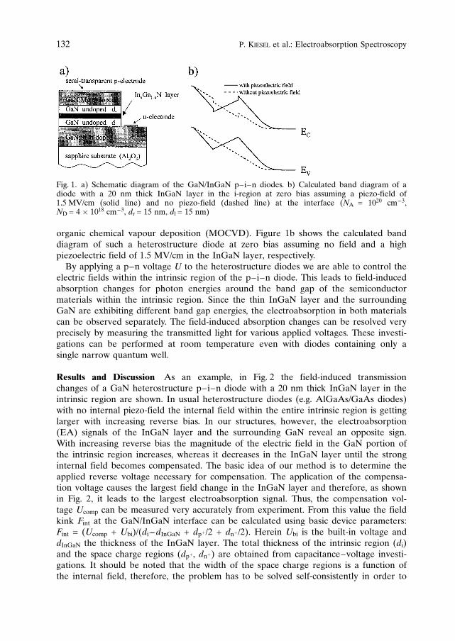
Results and Discussion As an example, in Fig. 2 the field-induced transmissionchanges of a GaN heterostructure p–i–n diode with a 20 nm thick InGaN layer in theintrinsic region are shown. In usual heterostructure diodes (e.g. AlGaAs/GaAs diodes)with no internal piezo-field the internal field within the entire intrinsic region is gettinglarger with increasing reverse bias. In our structures, however, the electroabsorption(EA) signals of the InGaN layer and the surrounding GaN reveal an opposite sign.With increasing reverse bias the magnitude of the electric field in the GaN portion ofthe intrinsic region increases, whereas it decreases in the InGaN layer until the stronginternal field becomes compensated. The basic idea of our method is to determine theapplied reverse voltage necessary for compensation. The application of the compensa-tion voltage causes the largest field change in the InGaN layer and therefore, as shownin Fig. 2, it leads to the largest electroabsorption signal. Thus, the compensation vol-tage Ucomp can be measured very accurately from experiment. From this value the fieldkink Fint at the GaN/InGaN interface can be calculated using basic device parameters:Fint = (Ucomp + Ubi)/(di––dInGaN + dpþ/2 + dnþ/2). Herein Ubi is the built-in voltage anddInGaN the thickness of the InGaN layer. The total thickness of the intrinsic region (di)and the space charge regions (dpþ, dnþ) are obtained from capacitance–voltage investi-gations. It should be noted that the width of the space charge regions is a function ofthe internal field, therefore, the problem has to be solved self-consistently in order to
132 P. Kiesel et al.: Electroabsorption Spectroscopy
Fig. 1. a) Schematic diagram of the GaN/InGaN p–i–n diodes. b) Calculated band diagram of adiode with a 20 nm thick InGaN layer in the i-region at zero bias assuming a piezo-field of1.5 MV/cm (solid line) and no piezo-field (dashed line) at the interface (NA = 1020 cm––3,ND = 4 � 1018 cm––3, dr = 15 nm, dl = 15 nm)
get an accurate value for Fint. Under the assumption that the difference in the sponta-neous polarisation of GaN and InGaN is relatively small, the determined value for Fint
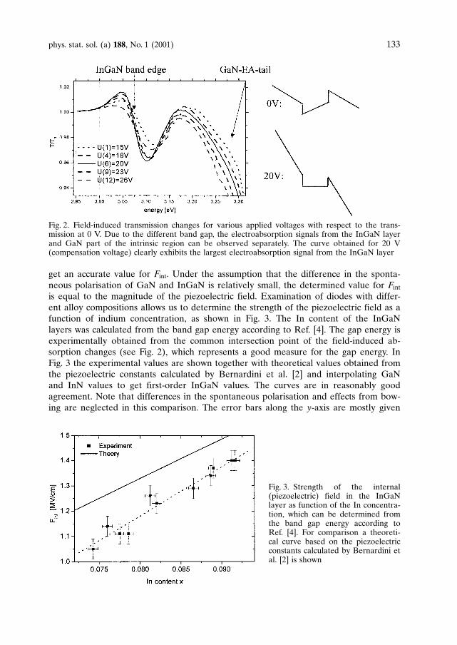
is equal to the magnitude of the piezoelectric field. Examination of diodes with differ-ent alloy compositions allows us to determine the strength of the piezoelectric field as afunction of indium concentration, as shown in Fig. 3. The In content of the InGaNlayers was calculated from the band gap energy according to Ref. [4]. The gap energy isexperimentally obtained from the common intersection point of the field-induced ab-sorption changes (see Fig. 2), which represents a good measure for the gap energy. InFig. 3 the experimental values are shown together with theoretical values obtained fromthe piezoelectric constants calculated by Bernardini et al. [2] and interpolating GaNand InN values to get first-order InGaN values. The curves are in reasonably goodagreement. Note that differences in the spontaneous polarisation and effects from bow-ing are neglected in this comparison. The error bars along the y-axis are mostly given
phys. stat. sol. (a) 188, No. 1 (2001) 133
Fig. 2. Field-induced transmission changes for various applied voltages with respect to the trans-mission at 0 V. Due to the different band gap, the electroabsorption signals from the InGaN layerand GaN part of the intrinsic region can be observed separately. The curve obtained for 20 V(compensation voltage) clearly exhibits the largest electroabsorption signal from the InGaN layer
Fig. 3. Strength of the internal(piezoelectric) field in the InGaNlayer as function of the In concentra-tion, which can be determined fromthe band gap energy according toRef. [4]. For comparison a theoreti-cal curve based on the piezoelectricconstants calculated by Bernardini etal. [2] is shown
due to the uncertainty in the determination of the space charge region from the C–Vmeasurements and the error from measuring Ucomp. The error with regard to the Incontent is due to the uncertainty in the experimental determination of the band gapenergy. A potential systematic error arising from the calculation of the In content fromthe gap energy according to Ref. [4] is neglected. Finally, I want to emphasis that usingthis technique the determination of internal field is not influenced by free carriers, be-cause the thin InGaN layer is incorporated in the intrinsic region of a p–i–n diode.
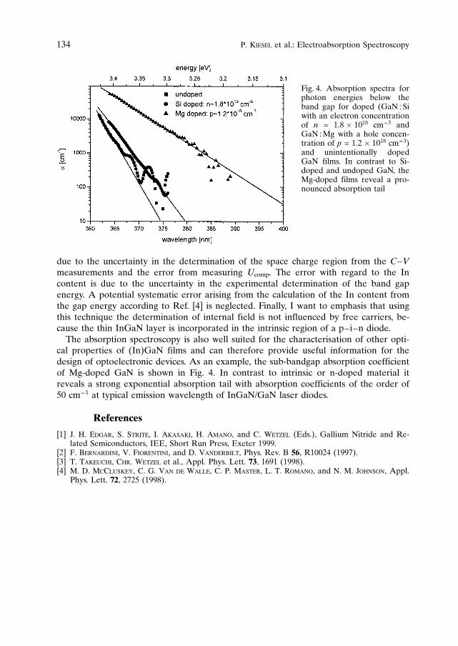
The absorption spectroscopy is also well suited for the characterisation of other opti-cal properties of (In)GaN films and can therefore provide useful information for thedesign of optoelectronic devices. As an example, the sub-bandgap absorption coefficientof Mg-doped GaN is shown in Fig. 4. In contrast to intrinsic or n-doped material itreveals a strong exponential absorption tail with absorption coefficients of the order of50 cm––1 at typical emission wavelength of InGaN/GaN laser diodes.
References
[1] J. H. Edgar, S. Strite, I. Akasaki, H. Amano, and C. Wetzel (Eds.), Gallium Nitride and Re-lated Semiconductors, IEE, Short Run Press, Exeter 1999.
[2] F. Bernardini, V. Fiorentini, and D. Vanderbilt, Phys. Rev. B 56, R10024 (1997).[3] T. Takeuchi, Chr. Wetzel et al., Appl. Phys. Lett. 73, 1691 (1998).[4] M. D. McCluskey, C. G. Van de Walle, C. P. Master, L. T. Romano, and N. M. Johnson, Appl.
Phys. Lett. 72, 2725 (1998).
134 P. Kiesel et al.: Electroabsorption Spectroscopy
Fig. 4. Absorption spectra forphoton energies below theband gap for doped (GaN : Siwith an electron concentrationof n = 1.8 � 1018 cm––3 andGaN : Mg with a hole concen-tration of p = 1.2 � 1018 cm––3)and unintentionally dopedGaN films. In contrast to Si-doped and undoped GaN, theMg-doped films reveal a pro-nounced absorption tail