electrical dependencies of optical modulation capabilities ... · electrical dependencies of...
TRANSCRIPT
Electrical dependencies of optical modulationcapabilities in digitally addressed parallelaligned liquid crystal on silicon devices
Francisco Javier Martínez,a,b Andrés Márquez,a,b,* Sergi Gallego,a,b Manuel Ortuño,a,b Jorge Francés,a,bAugusto Beléndez,a,b and Inmaculada Pascualb,caUniversidad de Alicante, Dept. de Física, Ing. de Sistemas y T. Señal, Ap. 99, Alicante E-03080, SpainbUniversidad de Alicante, I.U. Física Aplicada a las Ciencias y las Tecnologías, Ap. 99, Alicante E-03080, SpaincUniversidad de Alicante, Dept. de Óptica, Farmacología y Anatomía, Ap. 99, Alicante E-03080, Spain
Abstract. Parallel aligned liquid crystal on silicon (PA-LCoS) displays have found wide acceptance in applica-tions requiring phase-only modulation. Among LCoS devices, and PA-LCoS as a specific case, digital address-ing has become a very common technology. In principle, modern digital technology provides some benefits withrespect to analog addressing such as reduced interpixel cross-talk, lower power consumption and supply volt-age, gray level scale repeatability, high programmability, and noise robustness. However, there are also somedegradating issues, such as flicker, which may be enhanced. We analyze the characteristics of the digital pulsewidth modulated voltage signals in relation to their effect on the optical modulation capabilities of LCoS displays.We apply calibration techniques developed in our laboratory, basically the classical linear polarimeter extendedto take into account the existence of flicker. Various digital sequence formats are discussed, focusing the analy-sis on the variations in the magnitude of the applied voltages across the LC layer. From this analysis, we obtainhow to amplify the retardance dynamic range and how to enhance linearity in the device without enhancingflicker and without diminishing the number of available quantization levels. Electrical configurations intendedfor phase-only and intensity modulation regimes, useful in diffractive optics, are given. © 2014 Society of Photo-Optical Instrumentation Engineers (SPIE) [DOI: 10.1117/1.OE.53.6.067104]
Keywords: liquid crystal on silicon displays; parallel aligned; retardance measurement; phase-only modulation; spatial light modu-lation; flicker; diffractive optics; pulse width modulation.
Paper 140570P received Apr. 4, 2014; revised manuscript received May 20, 2014; accepted for publication May 22, 2014; publishedonline Jun. 24, 2014.
1 IntroductionLiquid crystal (LC) microdisplays have found widespreaduse as spatial light modulators (SLM) in applications suchas in diffractive optics,1 optical storage,2 optical metrology,3
reconfigurable interconnects,4,5 or quantum optical compu-ting.6 Among microdisplays, liquid crystal on silicon (LCoS)devices have become the most attractive system for theseapplications due to their very high spatial resolution andvery high light efficiency.7–9 LCoS displays are technologi-cally complex devices where the electrical signal appliedcontrols the optical transmission in each pixel. A propercharacterization and configuration of the main electricalparameters are crucial to generate the required optical modu-lation regimes in SLM applications, as exemplified by Luand Saleh10 with the previous analog liquid crystal displays(LCDs) taking into account the applied voltage dynamicrange and bias voltage. Interplay between electrical and opti-cal performance parameters has also been useful for identi-fying the origin for degradation effects in LCDs, such as theanamorphic and frequency dependent modulation,11 alsoreported in both digital12 and analog13 LCoS devices. Anadditional degradation effect detected in LCoS displays byseveral authors14–17 is that they produce phase flicker and/or depolarization, especially the ones with a digital back-plane18 due to the pulsed nature of the voltage signal
addressed.8,9,19,20 Among the different LC layer geometries,parallel aligned LCoS (PA-LCoS) devices are especiallyinteresting since they allow easy operation as phase-onlydevices without coupled amplitude modulation.8,9 No depo-larization operation is also available; however, they may stillexhibit phase fluctuations.18 Recently, we proposed a methodto characterize not only the linear retardance but also theamount of phase flicker in the optical signal21 valid for pa-rallel aligned LC devices. This method, the extended linearpolarimeter, has demonstrated its applicability to PA-LCoSdisplays21 exhibiting phase flicker; therefore, it can beused in the analysis of the influence of the electrical para-meters on the optical modulation performance propertiesof LCoS displays. This method is an elaboration of theclassical linear polarimeter which may be found to measurethe birefringence in LCs22 and in waveplates.23
As described by Lueder,24 pixel circuitry in the LCoS back-plane8,24–26 can be based on dynamic random-access memory(DRAM) or on static random-access memory (SRAM), whichis accordingly related to the differentiation between analogand digital addressing.27,28 If a memory is provided at thepixel in the form of an analog storage capacitor (DRAM)or digital memory circuit (SRAM), the array can be frame-addressed, i.e., all pixels are addressed simultaneously. Thishas the advantage of reducing the low frequency flickerof the line-addressed arrays, which was typical in LCDs.11
*Address all correspondence to: Andrés Márquez, E-mail: [email protected] 0091-3286/2014/$25.00 © 2014 SPIE
Optical Engineering 067104-1 June 2014 • Vol. 53(6)
Optical Engineering 53(6), 067104 (June 2014)
Downloaded From: http://opticalengineering.spiedigitallibrary.org/ on 07/16/2014 Terms of Use: http://spiedl.org/terms
Various reasons have motivated the introduction of digitalbackplanes in LCoS technology. The digital scheme is usu-ally more stable than analog and shows a repeatable perfor-mance. Field inversion is possible at the kilohertz range (e.g.,for each modulation pulse) without image retention. Thescheme does not suffer from electrical cross-talk (i.e., nolow pass filtering of the signal).29 A lower power consump-tion and a lower supply voltage are possible with the digitalbackplane.8,20 Digital driving can control the precise graylevel scale. Another advantage of pulse modulation is thatthe LC is driven between zero and saturation voltages in atime multiplexed fashion,26–28 so that the slow response ofswitching between adjacent voltage states is avoided. Thenematic LC responds to the root-mean-square (RMS) of theapplied waveform integrated over the switching time of theLC. However, the time varying AC modulation of the drivingvoltage is partially transferred to the LC and produces a tem-poral fluctuation or flicker of the reflected light as describedin Refs. 18–20, i.e., the electro-optical response of the SLMis not constant over the frame period. If the digital sequenceformat is properly chosen, fluctuations can be significantlydecreased to acceptable levels.21 To this goal, a proper cha-racterization not only of the phase modulation but also of theamount of phase flicker in the optical signal needs to bedone. This reasoning is not restricted to PA-LCoS devices,but it can be applicable in general to electro-optic variablelinear retarders such as the novel device proposed byRamirez et al.30 Apart from the sequence format, otheroptions (applied binary voltage value, selection of pulsecodes, and number of gray scale levels) offered by digitaladdressing need to be analyzed to produce proper phasedepth, enhanced linearity, number of quantization levelsavailable, etc.
In this work, we take advantage of the ease of imple-mentation and the effectiveness of the calibration methodproposed in Ref. 21 to characterize the basic electricalparameters controlling the digital signal addressed to a PA-LCoS display and their effect on the retardance dynamicrange and the magnitude of the flicker. Preliminary resultswere presented in Ref. 31. This enables us to produce elec-trical configurations specifically optimized for phase-only orfor amplitude-mostly modulation regimes.
2 Characterization Using the Extended LinearPolarimeter
In the following, we introduce the extended linear polari-meter proposed in Ref. 21, where the linear retarder undertest, in our case the PA-LCoS, is situated between two linearpolarizers illuminated with a monochromatic laser source. Inthe analysis shown in Ref. 21, it was demonstrated that theclassical technique based on measuring the intensity with aradiometer at the exit of the system for the parallel andcrossed configurations of the polarizers, both oriented at45 or −45 deg with respect to the neutral lines of thewaveplates, is not only a simple method but also the mostrobust to misalignments and other types of noise sourcesin the system. With respect to the classical technique, theextended linear polarimeter21 enables us to characterizethe retardance magnitude in the presence of retardance insta-bilities or flicker. Other techniques may also be applied;32,33
however, the present method is very straightforward to
implement and accurate enough for the study to be donein this work.
In the case of instabilities or fluctuations in the linearretardance, we demonstrated21 that as a first approximationfor PA-LCoS displays we may consider a model with a linearvariation of retardance with time ΓðtÞ. In this case, the aver-aged parallel and crossed polarizers intensities become
hIjjOUTi ¼I02
!sin aa
cos Γ̄"; (1)
hI⊥OUTi ¼I02
!sin aa
cos Γ̄"; (2)
where Γ̄ and a are the values for the average retardance andits flicker fluctuation amplitude, respectively. When combi-ning the two expressions, we obtain
hIjjOUTi − hI⊥OUTihIjjOUTiþ hI⊥OUTi
¼ sin aa
cos Γ̄; (3)
where we see that the cosine term becomes modulated by thepresence of a sinc function dependent on the magnitude ofthe fluctuation a. This sinc function represents the deviationfrom the classical expression typically used to obtain the li-near retardance value.21 Eventually, the average retardance Γ̄is obtained by inverting Eq. (3)
Γ̄ ¼ cos−1#hIjjOUTi − hI⊥OUTi∕hI
jjOUTiþ hI⊥OUTi
sin a∕a
$: (4)
In the case when no fluctuations exist (a ¼ 0 deg), thenEqs. (1)–(4) simplify into the classical results. We note thatEq. (4) returns the wrapped phase values in the range 0 to180 deg, which is the definition domain for the cos−1 func-tion. In general, the average retardance Γ̄ and the fluctuationamplitude a are coupled in Eqs. (1)–(4), yet at the maximaand minima (the extremals) the retardance value is known; itis a multiple of 180 deg (0 or 180 deg in the wrappeddomain). At these points, we may calculate the value for thefluctuation amplitude a and then it can be introduced inEq. (4) to produce a more accurate estimation of the averageretardance Γ̄ out of the extremals (what in Fig. 4 will becalled the “corrected” values). To obtain a, it was demon-strated that at the extremals, the absolute retardance diffe-rence Γdiff between the calculated and the true retardance val-ues is
Γdiff ¼ cos−1#sin aa
$: (5)
By inverting the set of numerical values (Γdiff ; a) providedby Eq. (5), we produce a fitting function enabling us to cal-culate a as a function of the value measured for Γdiff. Thisfitting function was calculated in Ref. 21 for a fluctuationamplitude a interval covering the range (0 deg, 110 deg)and is given by the linear expression
Optical Engineering 067104-2 June 2014 • Vol. 53(6)
Martínez et al.: Electrical dependencies of optical modulation capabilities. . .
Downloaded From: http://opticalengineering.spiedigitallibrary.org/ on 07/16/2014 Terms of Use: http://spiedl.org/terms
a ¼ 1.7795Γdiff : (6)
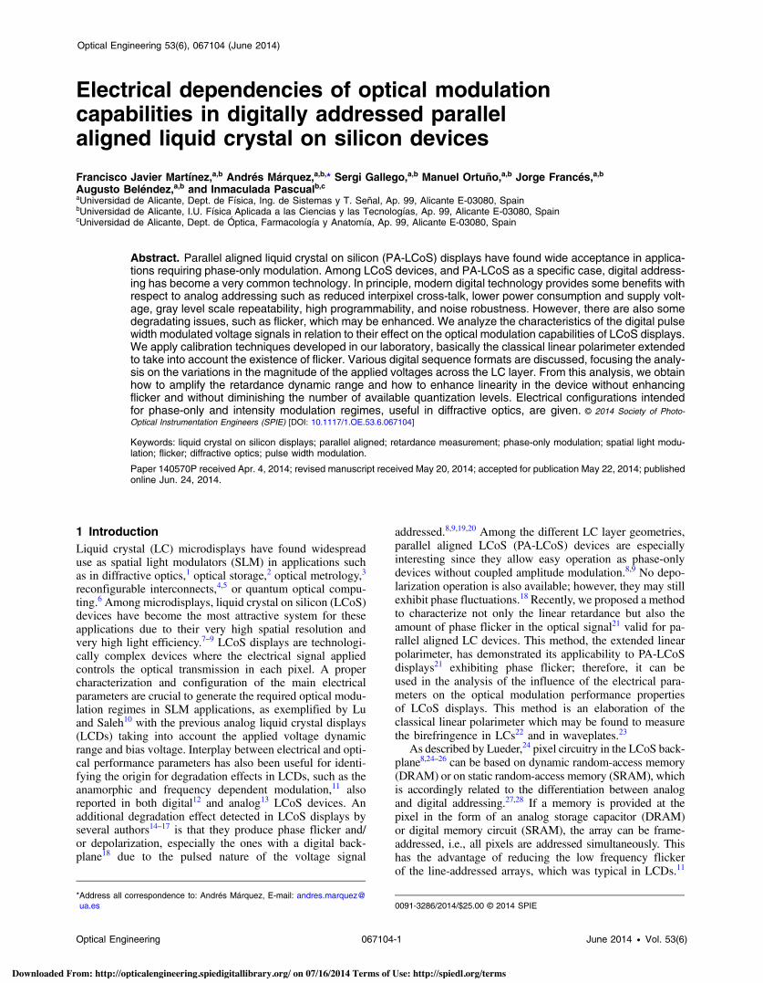
In Fig. 1, we present the experimental setup that we use inthis work to obtain the parallel and crossed polarizers inten-sities. The unexpanded beam from a He-Ne laser (633-nmwavelength) is incident onto a linear polarimeter where thereflective LCoS is the linear retarder to be measured. A quar-ter wavelength waveplate is added after the laser so thatenough light passes through the first polarizer irrespectiveof the orientation of its transmission axis. We consider qua-siperpendicular incidence at a 3-deg incidence angle onto theLCoS. We introduce one nonpolarizing cube beam splitter(NPBS) (model 10BC16NP.4, from Newport) to enableamplitude division with a 50/50 ratio of the reflectedbeam so that crossed and parallel intensities can be measuredsimultaneously (thus, two radiometers are introduced). Thisfurther enables synchronized measurement of the instantane-ous parallel and crossed polarizers intensity values simply byconnecting the two radiometers to the two channels of anoscilloscope (shown in this figure). The same setup is, there-fore, valid for the characterization of the average and theinstantaneous values. We note that in Ref. 21, we showedthat insertion of NPBS did not introduce significant polari-zation effects in the calibration when perpendicular inci-dence onto the beam splitter is considered as will be the casein this paper.
3 Digital Electrical Signal Addressing ParametersLet us provide the basic driving procedure to understand thegeneral parameters configuring the pulsed signal addressedin digital backplane LCoS displays. There are two steps:23,25
data addressing to the pixel SRAMmemory in the backplaneand LC driving. First, the input signal is processed by thecontroller and turned into bit-plane format. In this step, alook-up table (LUT) is used to determine the correct bitsequence for a target gray level. The first bit plane image iswritten to the pixel SRAM of the digital backplane, wherethe pixel memory has only “on” or “off” information. Theremay be a master and a slave memory enabling data to betransferred to a pixel at the same time that the previously
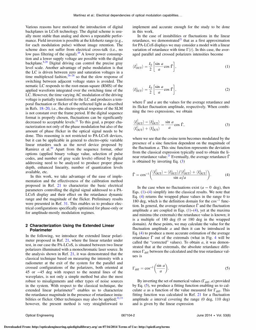
loaded data are being displayed. After the data-addressingstep is finished, the next step is to drive the LC wherethree voltage signal values, V0 and V1, low and high voltagesignals on the pixel backplane, and VITO, on the ITO trans-parent electrode on the glass substrate, are used. These volt-ages are applied to all pixels of the display area at the sametime so that every pixel is driven by the same condition. TheV0 and V1 signals are selected by the SRAM information ofthe pixel. Then, the driving voltage across the LC layer VLC
is given by VITO − V1 or VITO–V0, in the following Vbright
and Vdark, respectively. A schematic diagram for the absolutevalue of the digital signal VLC is shown in Fig. 2 (upper line),where the amplitudes for Vbright and Vdark are represented. Inthis driving scheme, the LC layer is driven by high frequencythat approximates a square wave running at several kilohertz.The nematic LC responds to the RMS value of the drivingvoltage over the switching time of the LC and the residualAC modulation is responsible for the flicker described in di-gital LCoS devices, represented in Fig. 2 (lower line). This iswhy it is generally understood that flicker noise can be mini-mized by high modulation rates.25,34
Fig. 1 Experimental setup used to measure the linear retardance as a function of the applied voltage(gray level) for a parallel aligned liquid crystal on silicon (LCoS). The setup allows both to measure aver-age and instantaneous values.
Fig. 2 Schematic diagram for the different voltage magnitudesinvolved in the digital addressing of the LCoS. Upper line driving volt-age V LC applied across the LC layer. Lower line voltage as seen bythe LC molecules.
Optical Engineering 067104-3 June 2014 • Vol. 53(6)
Martínez et al.: Electrical dependencies of optical modulation capabilities. . .
Downloaded From: http://opticalengineering.spiedigitallibrary.org/ on 07/16/2014 Terms of Use: http://spiedl.org/terms
The analysis in this paper deals with a digitally addressedphase-only LCoS, specifically the electrically controlledbirefringence LCoS display distributed by the companyHOLOEYE (Berlin, Germany). It is an active matrix reflec-tive mode device with 1920 × 1080 pixels and a 0.7 in.diagonal named the PLUTO SLM, with a pixel pitch of8.0 μm and a fill factor of 87%. The signal is addressedvia a standard digital visual interface signal. By means ofthe RS-232 interface and its corresponding provided soft-ware, we have access to the basic electrical parameters ofthe device19,20 previously described, such as the digitaladdressing sequence format (bit planes), the gamma curve,and the voltage dynamic range of the pulse width modulated(PWM) signal (through two digital potentiometers), i.e., volt-ages Vbright and Vdark.
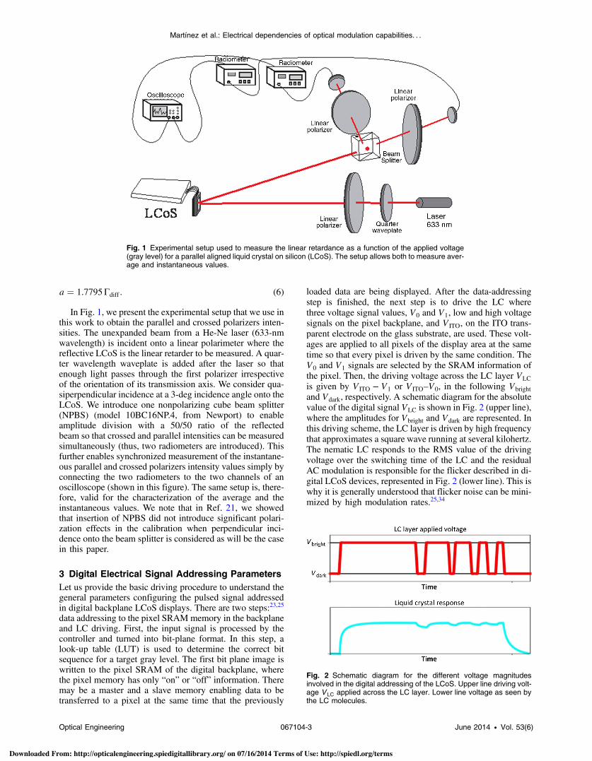
The software for the SLM is provided with a series ofconfiguration files corresponding to two different digitaladdressing sequences: the so-called 18-6 and 5-5 digitalsequences where the first number indicates the quantity of“equally weighted” bit planes and the second numberindicates the quantity of “binary” bit planes.19 This translatesinto a number of distinct voltage levels as follows: ð18þ 1Þ×26 ¼ 1216 for the sequence “18-6” and ð5þ 1Þ × 25 ¼ 192for the sequence “5-5.” The larger number of bit planesmakes the sequence 18-6 longer than the one correspondingfor the sequence 5-5. In principle, the shorter the sequence,the smaller the flicker,19 but on the other side, a largersequence provides a larger number of quantization levels.For each of the sequences, we find a series of configurationfiles which have been, in principle, optimized by the vendorfor different wavelengths to enable SLM users a fast accessto a proper operating configuration for the device adapted tothe specific application and illuminating wavelength. In ge-neral, these configuration files enable phase-only operationwith a 2π linear phase dynamic range for the specified wave-length. To this goal, the digital potentiometer values and thegamma curve, which corresponds to the LUT, need to beproperly selected.
In Sec. 2, we have presented an efficient and effectivetechnique able to discriminate, in terms of the average retar-dance dynamic range and the magnitude of the flicker,between the digital addressing sequences given with the soft-ware and driver electronics. Finer adjustment of the retar-dance dynamic range and its linearity is then feasible bymodifying the gamma curve and changing the digital poten-tiometers values. The simplicity of the linear polarimetersetup on which the method is based allows SLM users tohave access to adapt the calibration to their specific working
geometry and illuminating wavelength, adding novel pos-sibilities to the configuration files provided by the vendor.
In the rest of this paper, we focus on sequence 5-5 since itproduces less flicker than sequence 18-6, as previously com-mented on and as already demonstrated in a number ofpapers.19,35 By applying different gamma curves and differ-ent Vbright and Vdark voltages to a specific sequence we mayobtain very different retardance versus gray level curves. InFigs. 3(a)–3(c), we show three examples of gamma curvesfor the 5-5 sequence, corresponding, respectively, to the con-figuration files named “5-5 default ramp,” “5-5 linear 2pi633 nm,” and “5-5 linear 2pi 405 nm.” As we will showin Sec. 4.1, the first configuration provides the largest vol-tage modulation range available, thus enabling us to estimatethe maximum retardance dynamic range provided by theLCoS unit. The second and third configurations span aretardance range of 2π and π radians, respectively, which arethe necessary ranges to produce, respectively, a phase-onlyregime and an amplitude-mostly regime when using a va-riable linear retarder.
Figure 3(a) shows a linear mapping between the input andoutput values where all the 192 possible values associatedwith the 5-5 sequence are available. In Fig. 3(b), the mappingis highly nonlinear, especially for lower gray levels, and only95 out of the 192 possible values are available. In Fig. 3(c),the mapping is rather linear and a large quantity of gray le-vels, 175, are available.
With respect to the voltages Vbright and Vdark, we note thatboth the configuration file “5-5 default ramp” and “5-5 linear2pi 633 nm” have the same values, which are Vbright ¼3.82 V and Vdark ¼ 0.03 V. In the case of the configuration“5-5 linear 2pi 405 nm,” these values are Vbright ¼ 2.02 Vand Vdark ¼ 1.36 V. A change in these values affects thevoltage amplitude of the PWM pulses, thus affecting theaccumulated voltage experienced by the LC molecules in awhole frame period. We note that the largest voltage rangepossible is 3.82 to 0.03 V.
4 Results and Discussion
4.1 Initial ConfigurationsSome additional details are necessary to complement theexperiment description given in relation to Fig. 1. The in-tensities for both the parallel and crossed polarizer measure-ments have been obtained with the input polarizer transmis-sion axis at þ45 deg to the vertical of the laboratory, whichis the X-axis of our reference system. We note that the direc-tor for the LC (i.e., the extraordinary axis) in the LCoS isoriented along the horizontal, i.e., at þ90 deg with respect
Fig. 3 Gamma curves for the PLUTO LCoS for the configuration files: (a) “5-5 default ramp,” (b) “5-5linear 2pi 633 nm,” and (c) “5-5 linear 2pi 405 nm.”
Optical Engineering 067104-4 June 2014 • Vol. 53(6)
Martínez et al.: Electrical dependencies of optical modulation capabilities. . .
Downloaded From: http://opticalengineering.spiedigitallibrary.org/ on 07/16/2014 Terms of Use: http://spiedl.org/terms
to the X-axis. The director axis in nematic filled devices, as itis the case for our LCoS, typically corresponds to the slowaxis. Typically, the angular uncertainty on the orientation ofthe input and output polarizers with respect to the neutrallines of the LCoS can be considered to be %1 deg.
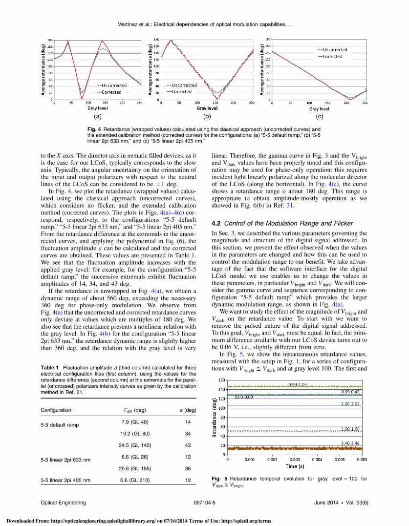
In Fig. 4, we plot the retardance (wrapped values) calcu-lated using the classical approach (uncorrected curves),which considers no flicker, and the extended calibrationmethod (corrected curves). The plots in Figs. 4(a)–4(c) cor-respond, respectively, to the configurations “5-5 defaultramp,” “5-5 linear 2pi 633 nm,” and “5-5 linear 2pi 405 nm.”From the retardance difference at the extremals in the uncor-rected curves, and applying the polynomial in Eq. (6), thefluctuation amplitude a can be calculated and the correctedcurves are obtained. These values are presented in Table 1.We see that the fluctuation amplitude increases with theapplied gray level: for example, for the configuration “5-5default ramp,” the successive extremals exhibit fluctuationamplitudes of 14, 34, and 43 deg.
If the retardance is unwrapped in Fig. 4(a), we obtain adynamic range of about 560 deg, exceeding the necessary360 deg for phase-only modulation. We observe fromFig. 4(a) that the uncorrected and corrected retardance curvesonly deviate at values which are multiples of 180 deg. Wealso see that the retardance presents a nonlinear relation withthe gray level. In Fig. 4(b) for the configuration “5-5 linear2pi 633 nm,” the retardance dynamic range is slightly higherthan 360 deg, and the relation with the gray level is very
linear. Therefore, the gamma curve in Fig. 3 and the Vbright
and Vdark values have been properly tuned and this configu-ration may be used for phase-only operation: this requiresincident light linearly polarized along the molecular directorof the LCoS (along the horizontal). In Fig. 4(c), the curveshows a retardance range o about 180 deg. This range isappropriate to obtain amplitude-mostly operation as weshowed in Fig. 6(b) in Ref. 31.
4.2 Control of the Modulation Range and FlickerIn Sec. 3, we described the various parameters governing themagnitude and structure of the digital signal addressed. Inthis section, we present the effect observed when the valuesin the parameters are changed and how this can be used tocontrol the modulation range to our benefit. We take advan-tage of the fact that the software interface for the digitalLCoS model we use enables us to change the values inthese parameters, in particular Vbright and Vdark. We will con-sider the gamma curve and sequence corresponding to con-figuration “5-5 default ramp” which provides the largerdynamic modulation range, as shown in Fig. 4(a).
We want to study the effect of the magnitude of Vbright andVdark on the retardance value. To start with we want toremove the pulsed nature of the digital signal addressed.To this goal, Vbright and Vdark must be equal. In fact, the mini-mum difference available with our LCoS device turns out tobe 0.06 V, i.e., slightly different from zero.
In Fig. 5, we show the instantaneous retardance values,measured with the setup in Fig. 1, for a series of configura-tions with Vbright ≅ Vdark and at gray level 100. The first and
Fig. 4 Retardance (wrapped values) calculated using the classical approach (uncorrected curves) andthe extended calibration method (corrected curves) for the configurations: (a) “5-5 default ramp,” (b) “5-5linear 2pi 633 nm,” and (c) “5-5 linear 2pi 405 nm.”
Table 1 Fluctuation amplitude a (third column) calculated for threeelectrical configuration files (first column), using the values for theretardance difference (second column) at the extremals for the paral-lel (or crossed) polarizers intensity curves as given by the calibrationmethod in Ref. 21.
Configuration Γdiff (deg) a (deg)
5-5 default ramp 7.9 (GL 40) 14
19.2 (GL 80) 34
24.5 (GL 140) 43
5-5 linear 2pi 633 nm 6.6 (GL 26) 12
20.6 (GL 155) 36
5-5 linear 2pi 405 nm 6.6 (GL 210) 12 Fig. 5 Retardance temporal evolution for gray level ¼ 100 forV dark ≅ V bright.
Optical Engineering 067104-5 June 2014 • Vol. 53(6)
Martínez et al.: Electrical dependencies of optical modulation capabilities. . .
Downloaded From: http://opticalengineering.spiedigitallibrary.org/ on 07/16/2014 Terms of Use: http://spiedl.org/terms
second values in each pair in the legend correspond, respec-tively, to Vdark and Vbright, ranging from (0.03 V, 0.09 V) to(3.40 V, 3.46 V), thus covering a wide voltage range. We seethat the curves show no flicker, in agreement with the factthat the pulse character in the digital signal is lost: boththe on and off bits addressed have equal voltage amplitudes.The fact that there are no temporal instabilities is also indica-tive that other origins for the flicker, such as thermal noise,can be disregarded. When applying other gray levels, theretardance values obtained remain the same and stable withtime. We note that there is a threshold value below which themolecules do not react. This can be seen because of the over-lap between the retardance curves for 0.03 and 0.39 V. Forhigher voltage values, retardance curves start to evolve anddo not overlap.
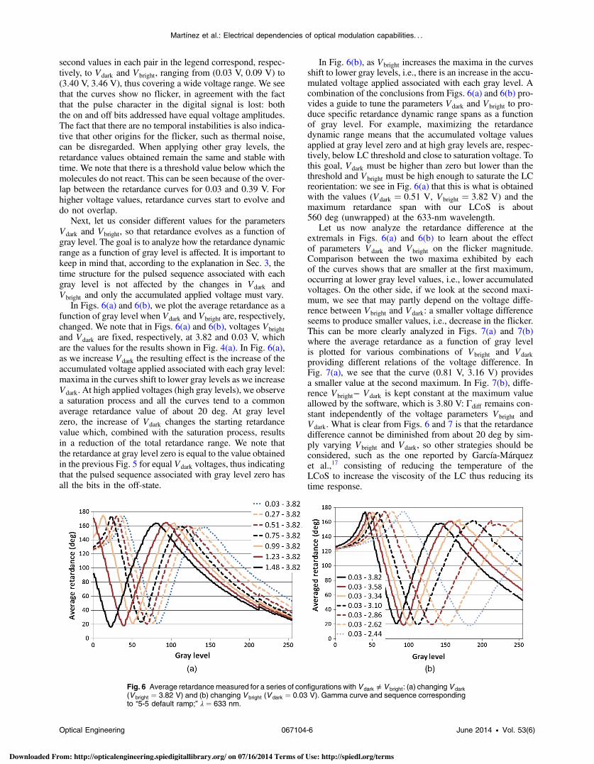
Next, let us consider different values for the parametersVdark and Vbright, so that retardance evolves as a function ofgray level. The goal is to analyze how the retardance dynamicrange as a function of gray level is affected. It is important tokeep in mind that, according to the explanation in Sec. 3, thetime structure for the pulsed sequence associated with eachgray level is not affected by the changes in Vdark andVbright and only the accumulated applied voltage must vary.
In Figs. 6(a) and 6(b), we plot the average retardance as afunction of gray level when Vdark and Vbright are, respectively,changed. We note that in Figs. 6(a) and 6(b), voltages Vbright
and Vdark are fixed, respectively, at 3.82 and 0.03 V, whichare the values for the results shown in Fig. 4(a). In Fig. 6(a),as we increase Vdark the resulting effect is the increase of theaccumulated voltage applied associated with each gray level:maxima in the curves shift to lower gray levels as we increaseVdark. At high applied voltages (high gray levels), we observea saturation process and all the curves tend to a commonaverage retardance value of about 20 deg. At gray levelzero, the increase of Vdark changes the starting retardancevalue which, combined with the saturation process, resultsin a reduction of the total retardance range. We note thatthe retardance at gray level zero is equal to the value obtainedin the previous Fig. 5 for equal Vdark voltages, thus indicatingthat the pulsed sequence associated with gray level zero hasall the bits in the off-state.
In Fig. 6(b), as Vbright increases the maxima in the curvesshift to lower gray levels, i.e., there is an increase in the accu-mulated voltage applied associated with each gray level. Acombination of the conclusions from Figs. 6(a) and 6(b) pro-vides a guide to tune the parameters Vdark and Vbright to pro-duce specific retardance dynamic range spans as a functionof gray level. For example, maximizing the retardancedynamic range means that the accumulated voltage valuesapplied at gray level zero and at high gray levels are, respec-tively, below LC threshold and close to saturation voltage. Tothis goal, Vdark must be higher than zero but lower than thethreshold and Vbright must be high enough to saturate the LCreorientation: we see in Fig. 6(a) that this is what is obtainedwith the values (Vdark ¼ 0.51 V, Vbright ¼ 3.82 V) and themaximum retardance span with our LCoS is about560 deg (unwrapped) at the 633-nm wavelength.
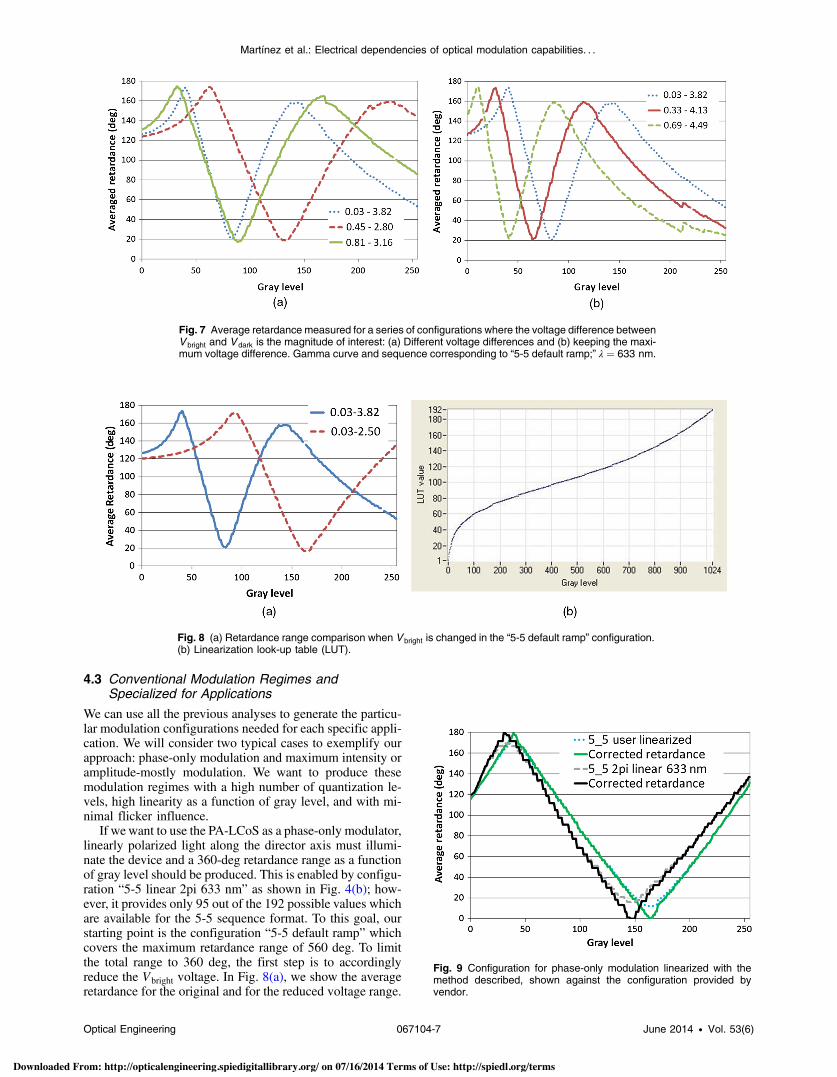
Let us now analyze the retardance difference at theextremals in Figs. 6(a) and 6(b) to learn about the effectof parameters Vdark and Vbright on the flicker magnitude.Comparison between the two maxima exhibited by eachof the curves shows that are smaller at the first maximum,occurring at lower gray level values, i.e., lower accumulatedvoltages. On the other side, if we look at the second maxi-mum, we see that may partly depend on the voltage diffe-rence between Vbright and Vdark: a smaller voltage differenceseems to produce smaller values, i.e., decrease in the flicker.This can be more clearly analyzed in Figs. 7(a) and 7(b)where the average retardance as a function of gray levelis plotted for various combinations of Vbright and Vdark
providing different relations of the voltage difference. InFig. 7(a), we see that the curve (0.81 V, 3.16 V) providesa smaller value at the second maximum. In Fig. 7(b), diffe-rence Vbright− Vdark is kept constant at the maximum valueallowed by the software, which is 3.80 V: Γdiff remains con-stant independently of the voltage parameters Vbright andVdark. What is clear from Figs. 6 and 7 is that the retardancedifference cannot be diminished from about 20 deg by sim-ply varying Vbright and Vdark, so other strategies should beconsidered, such as the one reported by García-Márquezet al.,17 consisting of reducing the temperature of theLCoS to increase the viscosity of the LC thus reducing itstime response.
Fig. 6 Average retardancemeasured for a series of configurations withV dark ≠ V bright: (a) changing V dark(V bright ¼ 3.82 V) and (b) changing V bright (V dark ¼ 0.03 V). Gamma curve and sequence correspondingto “5-5 default ramp;” λ ¼ 633 nm.
Optical Engineering 067104-6 June 2014 • Vol. 53(6)
Martínez et al.: Electrical dependencies of optical modulation capabilities. . .
Downloaded From: http://opticalengineering.spiedigitallibrary.org/ on 07/16/2014 Terms of Use: http://spiedl.org/terms
4.3 Conventional Modulation Regimes andSpecialized for Applications
We can use all the previous analyses to generate the particu-lar modulation configurations needed for each specific appli-cation. We will consider two typical cases to exemplify ourapproach: phase-only modulation and maximum intensity oramplitude-mostly modulation. We want to produce thesemodulation regimes with a high number of quantization le-vels, high linearity as a function of gray level, and with mi-nimal flicker influence.
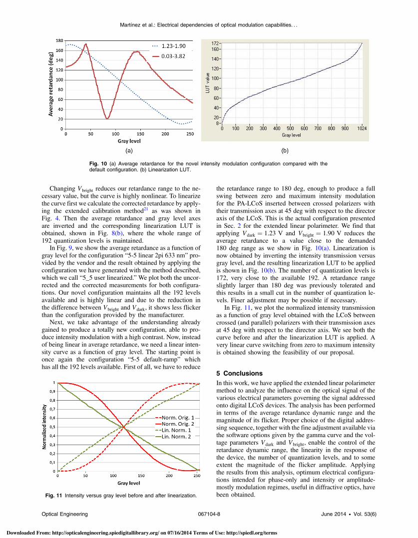
If we want to use the PA-LCoS as a phase-only modulator,linearly polarized light along the director axis must illumi-nate the device and a 360-deg retardance range as a functionof gray level should be produced. This is enabled by configu-ration “5-5 linear 2pi 633 nm” as shown in Fig. 4(b); how-ever, it provides only 95 out of the 192 possible values whichare available for the 5-5 sequence format. To this goal, ourstarting point is the configuration “5-5 default ramp” whichcovers the maximum retardance range of 560 deg. To limitthe total range to 360 deg, the first step is to accordinglyreduce the Vbright voltage. In Fig. 8(a), we show the averageretardance for the original and for the reduced voltage range.
Fig. 7 Average retardance measured for a series of configurations where the voltage difference betweenV bright and V dark is the magnitude of interest: (a) Different voltage differences and (b) keeping the maxi-mum voltage difference. Gamma curve and sequence corresponding to “5-5 default ramp;” λ ¼ 633 nm.
Fig. 8 (a) Retardance range comparison when V bright is changed in the “5-5 default ramp” configuration.(b) Linearization look-up table (LUT).
Fig. 9 Configuration for phase-only modulation linearized with themethod described, shown against the configuration provided byvendor.
Optical Engineering 067104-7 June 2014 • Vol. 53(6)
Martínez et al.: Electrical dependencies of optical modulation capabilities. . .
Downloaded From: http://opticalengineering.spiedigitallibrary.org/ on 07/16/2014 Terms of Use: http://spiedl.org/terms
Changing Vbright reduces our retardance range to the ne-cessary value, but the curve is highly nonlinear. To linearizethe curve first we calculate the corrected retardance by apply-ing the extended calibration method21 as was shown inFig. 4. Then the average retardance and gray level axesare inverted and the corresponding linearization LUT isobtained, shown in Fig. 8(b), where the whole range of192 quantization levels is maintained.
In Fig. 9, we show the average retardance as a function ofgray level for the configuration “5-5 linear 2pi 633 nm” pro-vided by the vendor and the result obtained by applying theconfiguration we have generated with the method described,which we call “5_5 user linearized.” We plot both the uncor-rected and the corrected measurements for both configura-tions. Our novel configuration maintains all the 192 levelsavailable and is highly linear and due to the reduction inthe difference between Vbright and Vdark, it shows less flickerthan the configuration provided by the manufacturer.
Next, we take advantage of the understanding alreadygained to produce a totally new configuration, able to pro-duce intensity modulation with a high contrast. Now, insteadof being linear in average retardance, we need a linear inten-sity curve as a function of gray level. The starting point isonce again the configuration “5-5 default-ramp” whichhas all the 192 levels available. First of all, we have to reduce
the retardance range to 180 deg, enough to produce a fullswing between zero and maximum intensity modulationfor the PA-LCoS inserted between crossed polarizers withtheir transmission axes at 45 deg with respect to the directoraxis of the LCoS. This is the actual configuration presentedin Sec. 2 for the extended linear polarimeter. We find thatapplying Vdark ¼ 1.23 V and Vbright ¼ 1.90 V reduces theaverage retardance to a value close to the demanded180 deg range as we show in Fig. 10(a). Linearization isnow obtained by inverting the intensity transmission versusgray level, and the resulting linearization LUT to be appliedis shown in Fig. 10(b). The number of quantization levels is172, very close to the available 192. A retardance rangeslightly larger than 180 deg was previously tolerated andthis results in a small cut in the number of quantization le-vels. Finer adjustment may be possible if necessary.
In Fig. 11, we plot the normalized intensity transmissionas a function of gray level obtained with the LCoS betweencrossed (and parallel) polarizers with their transmission axesat 45 deg with respect to the director axis. We see both thecurve before and after the linearization LUT is applied. Avery linear curve switching from zero to maximum intensityis obtained showing the feasibility of our proposal.
5 ConclusionsIn this work, we have applied the extended linear polarimetermethod to analyze the influence on the optical signal of thevarious electrical parameters governing the signal addressedonto digital LCoS devices. The analysis has been performedin terms of the average retardance dynamic range and themagnitude of its flicker. Proper choice of the digital addres-sing sequence, together with the fine adjustment available viathe software options given by the gamma curve and the vol-tage parameters Vdark and Vbright, enable the control of theretardance dynamic range, the linearity in the response ofthe device, the number of quantization levels, and to someextent the magnitude of the flicker amplitude. Applyingthe results from this analysis, optimum electrical configura-tions intended for phase-only and intensity or amplitude-mostly modulation regimes, useful in diffractive optics, havebeen obtained.
Fig. 10 (a) Average retardance for the novel intensity modulation configuration compared with thedefault configuration. (b) Linearization LUT.
Fig. 11 Intensity versus gray level before and after linearization.
Optical Engineering 067104-8 June 2014 • Vol. 53(6)
Martínez et al.: Electrical dependencies of optical modulation capabilities. . .
Downloaded From: http://opticalengineering.spiedigitallibrary.org/ on 07/16/2014 Terms of Use: http://spiedl.org/terms
AcknowledgmentsThis work was supported by the Ministerio de Trabajo yCompetitividad of Spain (projects FIS2011-29803-C02-01and FIS2011-29803-C02-02), by the Generalitat Valencianaof Spain (projects PROMETEO/2011/021 and ISIC/2012/013), and by the Universidad de Alicante (project GRE12-14).
References1. J. Turunen and F.Wyrowski, Eds.,Diffractive Optics for Industrial and
Commercial Applications, Akademie Verlag, Berlin (1997).2. H. J. Coufal, D. Psaltis, and B. T. Sincerbox, Eds., Holographic Data
Storage, Springer-Verlag, Berlin (2000).3. W. Osten, C. Kohler, and J. Liesener, “Evaluation and application
of spatial light modulators for optical metrology,” Opt. Pura Apl.38(3), 71–81 (2005).
4. M. A. F. Roelens et al., “Dispersion trimming in a reconfigurable wave-length selective switch,” J. Lightwave Technol. 26(1), 73–78 (2008).
5. M. Salsi et al., “Mode-division multiplexing of 2 100 Gb∕s channelsusing an LCOS-based spatial modulator,” J. Lightwave Technol. 30(4),618–623 (2012).
6. M. A. Solís-Prosser et al., “Preparing arbitrary pure states of spatialqudits with a single phase-only spatial light modulator,” Opt. Lett.38(22), 4762–4765 (2013).
7. S. T. Wu and D. K. Yang, Reflective Liquid Crystal Displays, JohnWiley & Sons Inc., Chichester (2005).
8. N. Collings et al., “The applications and technology of phase-onlyliquid crystal on silicon devices,” J. Display Technol. 7(3), 112–119 (2011).
9. Z. Zhang et al., “High quality assembly of phase-only liquid crystal onsilicon (LCOS) devices,” J. Display Technol. 7(3), 120–126 (2011).
10. K. Lu and B. E. A. Saleh, “Theory and design of the liquid crystal TVasan optical spatial phase modulator,” Opt. Eng. 29(3), 240–246 (1990).
11. A. Márquez et al., “Electrical origin and compensation for two sourcesof degradation of the spatial frequency response exhibited by liquidcrystal displays,” Opt. Eng. 46(11), 114001 (2007).
12. L. Lobato et al., “Characterization of the anamorphic and spatialfrequency dependent phenomenon in liquid crystal on silicon dis-plays,” J. Eur. Opt. Soc. Rapid Pub. 6, 11012S (2011).
13. J. Albero et al., “Second order diffractive optical elements in a spatiallight modulator with large phase dynamic range,” Opt. Lasers Eng.51(2), 111–115 (2013).
14. J. E. Wolfe and R. A. Chipman, “Polarimetric characterization ofliquid-crystal-on-silicon panels,” Appl. Opt. 45(8), 1688–1703 (2006).
15. P. Clemente et al., “Use of polar decomposition of Mueller matrices foroptimizing the phase response of a liquid-crystal-on-silicon display,”Opt. Express 16(3), 1965–1974 (2008).
16. A. Lizana et al., “Time-resolved Mueller matrix analysis of a liquidcrystal on silicon display,” Appl. Opt. 47(23), 4267–4274 (2008).
17. J. García-Márquez et al., “Flicker minimization in an LCoS spatiallight modulator,” Opt. Express 20(8), 8431–8441 (2012).
18. A. Lizana et al., “Influence of the temporal fluctuations phenomena onthe ECB LCoS performance,” Proc. SPIE 7442, 74420G (2009).
19. A. Hermerschmidt et al., “Wave front generation using a phase-onlymodulating liquid-crystalbased micro-display with HDTV resolution,”Proc. SPIE 6584, 65840E (2007).
20. J. R. Moore et al., “The silicon backplane design for an LCOS polari-zation-insensitive phase hologram SLM,” IEEE Photonic Technol.Lett. 20(1), 60–62 (2008).
21. F. J. Martínez et al., “Extended linear polarimeter to measure retard-ance and flicker: application to LCoS devices in two working geom-etries,” Opt. Eng. 53(1), 014105 (2014).
22. S. T. Wu, U. Efron, and L. D. Hess, “Birefringence measurements ofliquid crystals,” Appl. Opt. 23(21), 3911–3915 (1984).
23. A. Márquez et al., “Characterization of the retardance of a wave plateto increase the robustness of amplitude-only and phase-only modula-tions of a liquid crystal display,” J. Mod. Opt. 52(4), 633–650 (2005).
24. E. Lueder, “Liquid crystal on silicon displays,” in Liquid CrystalDisplays: Addressing Schemes and Electro-Optical Effects,” 2nded., pp. 353–361, John Wiley & Sons, Chichester (2010).
25. JVC Newsroom, Electronic Home Expo 2007, Press Release, “D-ILA™ Projector Technology: the path to high resolution projectiondisplays,” http://pro.jvc.com/pro/pr/2007/ehexpo/dila_wpaper.pdf (1November 2013).
26. J. Van den Steen, “Design of LCOS microdisplay backplanes for pro-jection applications,” pp. 136, Ph.D. Thesis, Gent University, Gent,Belgium (2006).
27. C. Cui-ying et al., “Study of the methods to realize gray scale for LCoSbased on sub-frame modulation,” in Proc. of the Symposium onPhotonics and Optoelectronics (SOPO), IEEE, New York (2011).
28. J.-S. Kang and O.-K. Kwon, “Digital driving method for low framefrequency and 256 gray scales in liquid crystal on silicon panels,”J. Display Technol. 8(12), 723–729 (2012).
29. G. Lazarev et al., “LCOS spatial light modulators: trends and appli-cations,” in Optical Imaging and Metrology: AdvancedTechnologies, W. Osten and N. Reingand, Eds., pp. 1–29, JohnWiley & Sons, Weinheim (2012).
30. C. Ramirez et al., “Point diffraction interferometer with a liquid crystalmonopixel,” Opt. Express 21(7), 8116–8124 (2013).
31. A. Márquez et al., “Study of the modulation capabilities of parallelaligned liquid crystal on silicon displays,” Proc. SPIE 8855,885504 (2013).
32. C. Ramirez et al., “Polarimetric method for liquid crystal displays char-acterization in presence of phase fluctuations,” Opt. Express 21(3),3182–3192 (2013).
33. F. J. Martínez et al., “Retardance and flicker modeling and characteri-zation of electrooptic linear retarders by averaged Stokes polarimetry,”Opt. Lett. 39(4), 1011–1014 (2014).
34. Jasper Display Corporation News, “FPD 2012 Jasper Announced1080p LCOS for phase modulation,” http://www.jasperdisplay.com/news/detail/308/ (1 November 2013).
35. A. Lizana et al., “The minimum Euclidean distance principle appliedto improve the modulation diffraction efficiency in digitally con-trolled spatial light modulators,” Opt. Express 18(10), 10581–10593 (2010).
Francisco Javier Martínez received his BS degree in electronic engi-neering from University of Valencia in 1996 and his BS degree inphysics in 1999. Currently, he is a research assistant with the AppliedPhysics to Science and Technology Institute from University of Ali-cante, and assistant professor of electronics at Miguel HernandezUniversity. His research interests include diffractive optics andholography.
Andrés Márquez received his MSc and PhD degrees in physics fromUniversidad Autónoma de Barcelona in 1997 and 2001, respectively.In 2000, he joined the Universidad de Alicante, where he is an asso-ciate professor of applied physics. His research interests include holo-graphic recording materials, liquid crystal spatial light modulators,optical image processing, and diffractive optics.
Sergi Gallego obtained his Msc degree in physics at University ofValencia in 2001 and his PhD degree at the University of Alicante,Spain, in 2005, where he works as a lecturer. His research interestsinclude holographic recording materials, diffraction, liquid crystal dis-plays applied to holography, diffractive elements, and photopolymers.He has authored or coauthored 1 patent and more than 60 publica-tions in renowned international journals.
Manuel Ortuño received his MSc degree in organic chemistry fromthe University of Murcia, Spain, in 1993. He received his MSc degreein chemical engineering in 1999 and a PhD degree in physics from theUniversity of Alicante, Spain, in 2005. In 2004, he joined theUniversidad de Alicante, where he is an associate professor. Hisresearch interests include light sensitive materials, photopolymers,holographic recording materials, liquid crystals, dyes and greenmaterials.
Jorge Francés received a PhD degree at the University of Alicante in2011. He received his MSEE in 2009 and his BSEE in 2006, both fromthe Technical University of Valencia, Valencia, Spain. He has beenworking as an assistant lecturer with the University of Alicantesince 2008. His main research interests include physical optics,sound and vibration, and numerical simulation.
Augusto Beléndez received his MSc degree and PhD degree inphysics from the University of Valencia, Spain, in 1986 and 1990,respectively. In 1996 he became full professor of applied physicsat the University of Alicante. He is mainly interested in holography,holographic recording materials, holographic optical elements, opticalprocessing, nonlinear oscillations and teaching of physics and engi-neering. He has published more than 250 technical papers and pre-sented more than 210 papers at scientific conferences.
Inmaculada Pascual received her MSc degree in physics from Uni-versity of Granada in 1985 and her PhD degree from University ofValencia in 1990. She is a full professor of optics at the Universityof Alicante. She has carried out research in holography, mainly onholographic recording material, holographic optical elements, andoptical data storage. She has published more than 125 papers andpresented more than 170 papers at scientific conferences.
Optical Engineering 067104-9 June 2014 • Vol. 53(6)
Martínez et al.: Electrical dependencies of optical modulation capabilities. . .
Downloaded From: http://opticalengineering.spiedigitallibrary.org/ on 07/16/2014 Terms of Use: http://spiedl.org/terms