efficient and sustained photoelectrochemical...
TRANSCRIPT
S1
Supporting information for
Efficient and Sustained Photoelectrochemical Water Oxidation by Cobalt Oxide/Silicon Photoanodes with
Nanotextured Interfaces
Jinhui Yang,†‡ Karl Walczak,†‡ Eitan Anzenberg,†‡ Francesca M. Toma, †¶ Guangbi Yuan,§ Jeffrey Beeman,†‡ Adam Schwartzberg,ǁ Yongjing Lin, †‡+ Mark Hettick, †‡+ Ali Javey, †+ Joel W. Ager, †‡ Junko Yano,†§ Heinz Frei,†§ Ian D. Sharp*†§ †Joint Center for Artificial Photosynthesis (JCAP), Lawrence Berkeley National Laboratory, Berkeley, CA 94720, USA. ‡Material Sciences Division, ¶Chemical Science Division, §Physical Biosciences Division, and ǁMolecular Foundry, Lawrence Berkeley National Laboratory, Berkeley, CA 94720, USA +Electrical Engineering and Computer Sciences,University of California, Berkeley, CA, 94720, USA.
Experimental Details
Formation of p+n-Si junctions by diffusion or ion implantation
Starting substrates were single side polished Czochralski-grown n-type (P-doped) prime grade (100) Si wafers with resistivity of 3.0 - 10 Ω cm. Two separate methods were utilized for junction formation: drive-in diffusion and ion implantation, as described below. Diffused junction wafers were utilized for initial studies and process development. However, it was later determined that ion implanted junctions ultimately enabled higher photovoltages to be established with reduced series resistances. All trends in stability and performance were the same, whether junctions were formed via diffusion or ion implantation. Reference measurements of electrocatalytic activity were also performed on p+-Si (100) (B-doped) wafers with resistivity of 0.001-0.005 Ω cm-1. Junction formation via drive-in diffusion Prior to processing, the wafers were cleaned with a 10 min Piranha (H2O2:H2SO4) dip followed by 1 min HF acid (10:1) dip, with a DI water rinse after each step. Following these cleaning steps, the wafers were immediately loaded into an atmospheric pressure furnace, which was continuously purged with 5000 sccm N2 during heating and cooling phases. The chamber was closed and heated to 1050 °C. Once the atmospheric pressure furnace stabilized at 1050 °C, boron diffusion and activation were performed in a single step by flowing boron trichloride and helium (BCl3/He) at 180 sccm and H2/N2 at 3000 sccm into the chamber for 2.5 hour. The BCl3 and Si reacted with oxygen in the chamber, decomposing to B2O3 and SiO2 to form a borosilicate glass layer, as well as a small amount of silicon nitride. Next, the BCl3/He was turned-off, the chamber was cooled to 500 °C, and the wafers were removed from the furnace. Following the diffusion process, the wafers were soaked in BHF (5:1) for 45 minutes to remove the borosilicate glass layer. The sheet resistance was measured across the wafer to be, on average, 6-7 Ω/sq, confirming formation of a highly doped junction layer > 1020 cm-3. Processing of wafers was conducted in the Marvell Nanofabrication Laboratory at the University of California, Berkeley.
S2
Junction formation via ion implantation As an alternate, and ultimately superior, method to junction formation, ion implantation was employed. Room temperature implantation was performed at a 7° incident angle using 11B accelerated to 45 keV with a dose of 1×1014 cm-2 and 32 keV with a dose of 5×1014 cm-2. In order to reduce contact resistance, the backsides of the wafers were implanted with 31P at 140 keV with a dose of 1×1014 cm-2 and 75 keV with a dose of 5×1014 cm-2. Dopant activation, both for the junction p+ layer and the contact n+ layer, was achieved via rapid thermal annealing at 1000 °C for 15 s under flowing nitrogen. Verification of junction formation Solid state measurements were performed to verify successful junction formation. However, the purpose of these measurements was to confirm establishment of junction photovoltage and not to optimize for contact resistance or illuminated area. Electrical contact was made to the emitter and backside using a Ga-In eutectic. For the case of diffusion doped devices, the backside of the wafer was first phyically lapped to access the n-type base. A microprobe with a tungsten tip was used to make electrical contact to the liquid metal contact on the emitter – though opaque, illumination and collection from the periphery of the emitter contact were sufficient to verify junction formation and photovoltage. The current-voltage characteristics were measured using a Keithley 2400 source meter and a Solar Light 16S-300-005 simulator set at an irradiance of 100 mW/cm2 with an AM 1.5 filter set. Confirmation that all processes resulted in the establishment and retention of >500 mV open circuit voltage was ensured prior to detailed photoelectrochemical testing. Nanotexturing surfaces via substrate bias sputtering
Substrate bias sputtering was originally developed for surface cleaning of semiconductor surfaces prior to additional layer deposition, in which the formation of ideal interfaces is essential for realizing high performance.1 For this purpose, the bias should be well controlled to just remove a very thin layer of native oxide or other contaminant species from the surface of the wafer. The use of Ar ion bombardment was demonstrated to effectively reduce the silicon epitaxy temperature.2 Substrate bias sputtering has also been applied in combination with target bias to control the quality of deposition.3 In this paper, we made use of the substrate bias sputtering both to remove surface contamination and to achieve nanotextured surfaces of p+n-Si. The substrate bias sputtering of p+n-Si was performed with an AJA International ATC Orion 5 sputtering machine equipped with a load lock. The sputtering condition was optimized by changing the radio frequency (RF) power (5-15 W), Ar pressure (5-15 mTorr), and duration time (5-30 min). The p+n-Si substrate was first cleaned by sonication in DI water and then in isopropanol for 5 min each, followed by etching in buffered HF for 5 min immediately prior to the sputtering. XPS and solar cell characteristic measurements (solid state JV) were conducted immediately after sputtering. The optimal sputtering condition was determined (15 W, 10 mT Ar, and 10 min) by XPS to monitor the removal of remnant nitrogen from the drive-in diffusion process used for p+ doping of some wafers. Furthermore, solid state current-voltage characteristics were used to ensure that the open circuit voltage (Voc ) was not adversely affected and remained above 500 mV. Deposition of CoOx by atomic layer deposition (ALD)
Prior to ALD, all Si samples, including bias sputtered samples, were treated in buffered HF for 2 min to remove the native oxide formed by intermediate air exposure. The CoOx catalyst films were deposited using a remote plasma-enhanced atomic layer deposition (Oxford FLexAl) (ALD) process at 300 °C. Cobalt precursor was CoCp2 (98% Strem Chemicals) and oxygen plasma was the oxidant.4 The precursor lines, carrier gas lines, and the reactor walls were kept at 120 °C. The CoCp2 precursor bubbler was heated up to 80 °C and bubbled with 200 sccm high purity Ar gas during the precursor exposure half cycles. Oxygen gas flow was held constant at 60 sccm throughout the deposition process. The cobalt

S3
precursor exposure half cycle consisted of 5 s CoCp2 dosing and 5 s purging. The remote oxygen plasma half cycle consisted of 1 s pre-plasma treatment, 5 s plasma exposures, and 15 s purging. The applied plasma power was 300 W and was applied for 5 s during the oxygen plasma half cycle. The deposition chamber was maintained at 15 mTorr at all times. The film thicknesses were measured using UVISEL spectroscopic ellipsometer (Horiba Jobin Yvon). The average growth rate was 0.7 Å/cycle. Photoelectrochemical testing
Photoelectrochemical (PEC) linear sweep voltammetry and stability testing (chronoamperometry and chronopotentiometry) were performed using a Biologic potentiostat and a three electrode cell containing quartz windows using a platinum wire as counter electrode, a Hg/HgO (1 M NaOH) or Ag/AgCl (3 M NaCl) as reference electrode, and p+n-Si as the working electrode. Si working electrodes with area ranging from 0.2 to 0.8 cm2 were fabricated by scratching an indium-gallium eutectic (Aldrich) into the backside of the wafer and a fixing a copper wire using conductive silver epoxy (Circuit Works). The copper wire was passed through a glass tube and the wafer was insulated and attached to the glass tube with Loctite 615 Hysol Epoxi-patch or 7460 adhesive. Electrodes were dried overnight before testing. The supporting electrolyte was aqueous 1 M NaOH (pH13.6). For the long term stability test, a home-made Teflon photoelectrochemical cell that incorporates an O-ring compression sealing to the front of the sample, a copper rod contacting the backside of Si working electrodes, which was scratched by an indium-gallium eutectic (Aldrich), and a quartz window was also used. The effective area is about 0.26 cm2. All measurements were performed using an air saturated solution. PEC tests were performed at 100 mW/cm2 using a Solar Light 16S-300-005 solar simulator equipped with an AM1.5 filter set. All data were recorded following initial light-dark testing and without ohmic drop correction.
Cyclic voltammetry in ferri/ferrocynide aqueous solution (both 10 mM in 1 M KCl) was performed with a Biologic potentiostat using a Ag/AgCl (3M NaCl) reference electrode, a platinum wire as counter electrode, and CoOx/p+n-Si as working electrode cell with the same configuration as the PEC test described above. The voltammograms were recorded at sweep rates of 100 mV s-1.
Incident photon to current efficiency (IPCE) was measured in a home-built setup, using a 150 W Xenon lamp (Newport) coupled with a 1/8m Monochromator (Oriel) as the light source. The intensity of monochromatic light was calibrated with a Si photodiode (Thorlabs FDS100-CAL). The working electrode was biased at 1.5 V vs RHE with a Gamry Reference 600 potentialstat in a three electrode cell containing quartz windows and using a platinum wire as counter electrode, a Hg/HgO (1 M NaOH) as reference electrode, and CoOx/p+n-Si as the working electrode.
XPS measurements
X-ray photoelectron spectroscopy (XPS) was performed using a monochromatized Al Kα source (hν = 1486.6 eV), operated at 225 W, on a Kratos Axis Ultra DLD system at a takeoff angle of 0º relative to the surface normal, and pass energy for narrow scan spectra of 20 eV, corresponding to an instrument resolution of approximately 600 meV. Spectral fitting was done using Casa XPS analysis software. Spectral positions were corrected using adventitious carbon by shifting the C 1s core level position to 284.8 eV and curves were fit with quasi-Voigt lines following Shirley background subtraction.
AFM measurement
Atomic force microscopy (AFM) images were collected with a Bruker Dimension Icon operating in tapping mode using Bruker TAP150A probes (Sb doped Si; Spring constant: 5 N/m; Frequency: 150kHz),

S4
and ScanAsyst mode using Bruker ScanAsyst-Air probes (silicon tip; silicon nitride cantilever, spring constant: 0.4 N m−1,frequency: 70 KHz) for Si and CoOx/Si, respectively.
The scan size was typically 1 µm × 1 µm. The images were analyzed using the AFM software NanoScope version 1.5. Flattening was performed to remove curvature and slope from images. After flattening, the root mean square (rms) roughness was calculated. The rms roughness, Rq, is given by the standard deviation of the data:
𝑅𝑞 =�
� (𝑧𝑖 − 𝑧𝑎𝑣𝑔)2
𝑁
𝑖=0𝑁 − 1
where zavg is the average height value within the given area, zi is the height at point i, and N is the number of data points within a given area.
Cross-section TEM
CoOx/p+n Si samples were cleaved into two strips (~0.2x1 cm), carefully cleaned and glued with M-Bond® resin by the CoOx side (sample/glue/sample sandwich assembly). The sandwich was pressed and annealed for 90 min. Then TEM specimens were prepared by mechanical polishing (MultiPrep Polishing System 8”, Allied High Tech Product Inc), and by high precision polishing with ion abrasion at 4-100 eV at a temperature of ~ -120 ºC (PIPS II, Gatan). High resolution transmission electron microscopy images were obtained with a CM200 FEI microscope at 200 kV.
XANES measurement and data analysis
X-ray absorption near edge structure (XANES) spectra were collected at the Advanced Light Source (ALS) on Beamline 10.3.2. The radiation was monochromatized by a Si (111) double-crystal monochromator. The intensity of the incident X-ray was monitored by an N2-filled ionization chamber (I0) in front of the sample. The energy was calculated using a glitch in I0 relative to the absorption edge of a Co foil. All data were collected at room temperature. An X-ray grazing incidence angle of ~5° was employed for surface enhancement. Data reduction of the XAS spectra was performed using custom software. Pre-edge and post-edge contributions were subtracted from the XAS spectra, and the result was normalized with respect to the edge jump.

S5
Supplementary Figures
Figure S1. AFM images of p+n-Si by driven-in diffusion (a) before and (b) after CoOx depostion . The rms roughness (Rq) is increased from 1.3 to 2.9 nm.
Figure S2. Cross-section TEM images of CoOx/p+n Si by ion-implantation with nanotextured interfaces in a wide range.
(a) (b)

S6
Figure S3. Photocurrent density versus applied potential (J-E) curves of CoOx/p+n-Si with planar (black ) and nanotextured (red) interfaces as a function of number of ALD cycles. The growth rate, which was determined by ellipsometry measurement, was initially approximately 0.7 Angstrom per cycle, and became about 0.5 Angstrom per cycle with increasing cycles, so the overall thickness for 30, 60, 100 cycles were about 2, 3 and 5 nm, respectively. The thickness of 4-5 nm for 100 cycles sample was also confirmed from cross-section TEM. The p+n-Si devices shown here were made by the B diffusion process, which led to smaller photovoltages and more anodic onset potential than for the implanted p+n-Si devices shown in the main text. Nevertheless, nanotextured devices resulted in J-E enhancement compared to planar devices regardless of method for p+n-Si junction formation (see Fig. S3).
Figure S4. Photocurrent density versus applied potential (J-E) characteristics following 100 ALD cycles of CoOx on planar (black) and nanotextured (red) p+n-Si formed via ion implantation. As described in the main text, a larger saturation current density and improved photoanodic onset potential is obtained for
1.0 1.2 1.4 1.6 1.80
5
10
15
20
25
30 60 cycles
J (m
A c
m-2)
E ( V vs RHE)1.0 1.2 1.4 1.6 1.8
E (V vs RHE)
30 cycles
1.0 1.2 1.4 1.6 1.8
100 cycles
E (V vs RHE)

S7
nanostructured devices. Comparison to Figure S3 highlights the improved photoelectrochemical behavior for ion implanted devices compared to diffusion doped devices. This improvement is attributed to more precise control over doping in the p+ layer, as well as reduction of the back contact resistance via formation of an n+ contact layer. All trends of stability and performance were found to be the same, regardless of method of junction and back contact formation.
Figure S5. Incident-photon-to-current-efficiency (IPCE) measurement of 100 ALD cycles CoOx on p+n-Si with planar (black) and nanotextured (red) interfaces at a fixed bias voltage of 1.5 V vs. RHE in 1 M NaOH. Consistent with findings from J-E measurements (Figures S3 and S4), the quantum efficiency is improved for nanotextured devices compared to planar devices. The higher IPCE for the nanotextured sample at longer wavelengths indicates that reduced interfacial resistance promotes charge transfer over carrier recombination and is consistent with the observed increase of the saturation current density. However, at shorter wavelengths, light absorption and carrier generation occur closer to the surface of the silicon, where competition between surface recombination and interfacial charge transfer is more pronounced.5 The observation that IPCE is similar for both nanotextured and planar devices at short wavelengths reveals that surface recombination dominates for both types of photoelectrode when light absorption is localized to the near surface region. This result suggests that additional performance enhancements could be achieved by improved interface state passivation, which is an interesting direction but beyond the scope of the present work.

S8
Figure S6. Saturation current density dependence on light intensity for 100 ALD cycles CoOx on p+n-Si with planar (black) and nanotextured (red) interfaces in 1 M NaOH. For both materials, a linear dependence is found, indicating light-limited current. In addition, the saturation current density is larger for nanotextured devices compared to planar devices for all irradiances.
Figure S7. Cyclic voltammetry of CoOx/p+n-Si (100 ALD cycles) with planar (black) and nanotextured (red) interfaces under illumination in ferri/ferrocynide aqueous solution (both 10 mM in 1 M KCl). The peak-to-peak separation is 0.25 V on the nanotextured sample versus 1.2 V on the planar sample.
S9
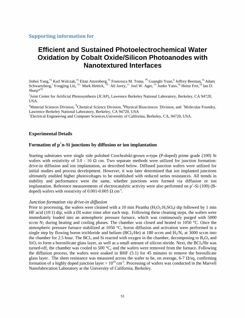
Figure S8. Chronoamperometry curves of CoOx/p+n-Si (drive-in diffusion, 60 ALD cycles) with planar (black) and nanotextured (red) interfaces at 1.6 V vs. RHE in 1 M NaOH under one sun illumination. The red and blue traces show the first and second sequential measurements, respectively, on the same nanotextured CoOx/p+n-Si device.
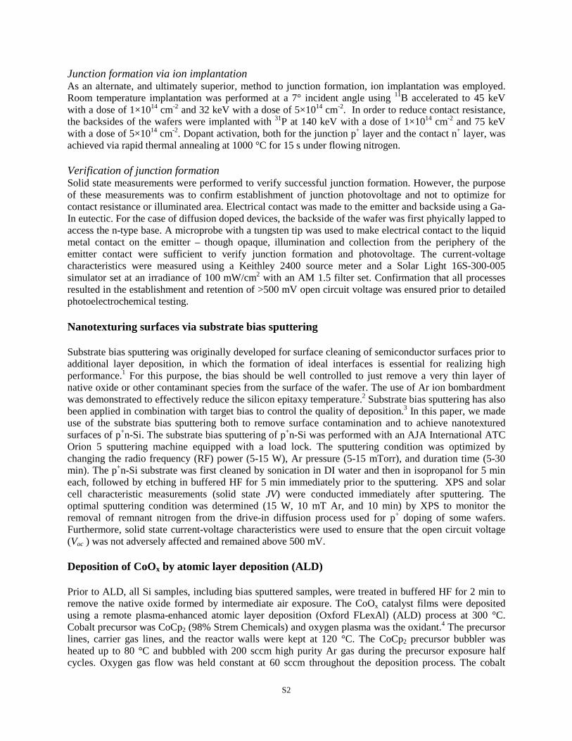
Figure S9. Comparison of J-E curves for planar (black) and nanotextured (red) CoOx/p+n-Si (60 ALD cycles) before (solid lines) and after (dashed lines) the stability tests shown in Figure S7. Planar devices are characterized by significant corrosion and a corresponding decline in photoelectrochemical J-E response, whereas no detectable degradation is observed for the case of nanotextured devices.
0 5 10 15 20 25 300
5
10
15
20
25
J (m
A c
m-2)
t (min)

S10
Figure S10 Co 2p XPS of nanotextured CoOx/p+n Si before (black) and after (red) 24 hours’ PEC test.
Figure S11 AFM images of ion implanted, nanotextured CoOx/p+n Si before (a) and after (b) PEC testing for 24 h.
810 805 800 795 790 785 780 775
Inte
nsity
(a.u
.)
Binding Energy (eV)
(a) (b)

S11
Figure S12 AFM images of ion-implanted CoOx/p+n Si with planar (a,b) and nanotextured (c,d) interfaces before (a,c) and after (b, d) soaking in 1 M NaOH for 24 hours .
Figure S13 Co 2p XPS of CoOx/p+n Si with planar (a) and nanotextured (b) interfaces before (black curves) and after (red curves) soaking in 1 M NaOH for 24 hours .
(a) (b)
(c) (d)

S12
Figure S14. Co 2p core level of CoOx on Si as a function of the number of ALD cycles. Although spin-orbit split Co 2p3/2 and Co 2p1/2 components are presented, all fitting and quoted binding energies refer to the Co 2p3/2 region. For the case of 10 ALD cycles of CoOx, the primary emission peak is observed at 780.7 eV, with a second peak at 782.5 eV and a clear satellite peak centered at 786.3 eV. With increasing number of ALD cycles, the primary emission peak shifts to lower binding energy: 780.2 eV for 30 cycles, 779.6 eV for 60 and 100 cycles. The second peak also shifts to lower BE for 30 cycles, and splits into two peaks at 781.0 and 782.3 eV for both 60 and 100 ALD cycles. The intensity of the 786.3 eV shake-up satellite decreases with increasing number of ALD cycles. An additional satellite peak at approximately 789.6 eV increases in intensity with increasing number of ALD cycles. As described in the main text, comparison of these features to reference spectra (Figure S15) and CoOx ALD literature reveals that thin CoOx ALD layers are dominated by Co(II). Though this could be in the form of Co(OH)2, it is likely to be CoO given the Co(Cp)2 and O2 precursors used for deposition. With increasing number of ALD cycles, the surface becomes dominated by Co3O4.
810 800 790 780 770
Inte
nsity
(a.u
.)
Binding Energy (eV)
10 cycles
30 cycles
60 cycles
100 cycles

S13
Figure S15. XPS of Co 2p core level spectra from Co3O4 (upper) and Co(OH)2 (lower) reference samples. Fitting of the Co 2p3/2 features was performed using parameters from the literature.6,7 The main differences are: (1) the primary emission peak shifts from 780.7 eV for Co(OH)2 to a lower binding energy (BE), 779.6 eV, for Co3O4; (2) the second strong emission peak of Co(OH)2 at 782.3 eV splits into two peaks for Co3O4; (3) a strong shake-up satellite peak at 786.3 eV, which is characteristic of Co(II), is strong for Co(OH)2 but has a significantly reduced intensity for Co3O4; (4) the intensity of the satellite peak at 789.6 eV is stronger in Co3O4 than that in Co(OH)2. As described in the text and shown in Figure S14, these features are used to determine the composition of the CoOx as a function of number of ALD cycles.
Figure S16. XPS of Co 2p core level spectra of CoOx/p+n Si-before and after PEC testing for 1 hour. Fitting of the Co 2p3/2 features was performed using parameters from the literature.6,7 The surface composition is transformed from Co3O4 to CoO(OH), which is characterized by the distinct shift of Co 2p core level emission to larger binding energies, and the emergence of a strong hydroxide-related peak in the O1s region (see Figure S17).
Binding Energy (eV)
Inte
nsity
(a.u
.)
CoOx/p+nSiafterPEC
CoOx/p+nSi

S14
Figure S17. XPS of the O 1s core level region for nanostructured CoOx/p+n-Si (60 ALD cycles) before (black) and after (red) the 1 h PEC stability test in Figure S8. Curve fitting was performed using parameters from literature.6-7 Comparison of O 1s spectra reveals the presence of a relatively narrow peak at 530.0 eV from CoOx. The presence of an additional broad peak at higher binding energy can be assigned to hydroxyl groups, as well as some contribution from adsorbed water. The rise of this emission peak following PEC testing is consistent with formation of CoO(OH). Though the area ratio of the low and high binding energy peaks should be approximately 1:1 for CoO(OH), water adsorption both before and after reaction leads to additional spectral intensity in the higher binding energy region. However, analysis of the Co 2p core level region (see main text) provides additional evidence for CoO(OH) formation.
References
(1) Burger, W. R.; Reif, R. J. Appl. Phys. 1987, 62, 4255. (2) Ohmi, T.; Ichikawa, T.; Shibata, T.; Matsudo, K.; Iwabuchi, H. Appl. Phys. Lett. 1988, 53, 45. (3) Sundgren, J. E.; Johansson, B. O.; Hentzell, H. T. G.; Karlsson, S. E. Thin Solid Films 1983, 105, 385. (4) Donders, M.; Knoops, H.; Kessels, W.; Notten, P. J. Electrochem. Soc. 2011, 158, G92. (5) Sze, S.; 2 ed.; John Wiley & Sons, New York: 1981; Vol. 14, p 799. (6) Biesinger, M. C.; Payne, B. P.; Grosvenor, A. P.; Lau, L. W. M.; Gerson, A. R.; Smart, R. S. C. Appl. Surf. Sci. 2011, 257, 2717. (7) Yang, J.; Liu, H.; Martens, W. N.; Frost, R. L. J. Phys. Chem. C 2009, 114, 111.