effect of the electrophoretic deposition of au nps in the ... · pdf fileof the...
TRANSCRIPT
Electrochimica Acta 188 (2016) 710–717
Effect of the electrophoretic deposition of Au NPs in the performanceCdS QDs sensitized solar Cells
I. Zarazúaa,c, D. Esparzaa, T. López-Lukea, A. Ceja-Fdeza, J. Reyes-Gomezb, I. Mora-Seróc,E. de la Rosaa,*aCentro de Investigaciones en Óptica, A.P. 1-948 León, Gto. 37150, Mexicob Facultad de Ciencias, Universidad de Colima, Colima Col. 28045, Mexicoc Institute of Advanced Materials, Universitat Jaume I, 12071 Castelló, Spain
A R T I C L E I N F O
Article history:Received 8 July 2015Received in revised form 19 November 2015Accepted 25 November 2015Available online 27 November 2015
Keywords:Solar CellsQuantum dotsImpedance spectroscopyAu Nanoparticles
A B S T R A C T
Solution-processed mesoscopic oxide semiconductor-based materials offer potentially low-cost and highstability alternative for next generation of solar cells, and metallic nanoparticles had shown to be a goodalternative to improve specific parameters in such kind of devices. In the present work, it is showed thesystematic study of the effect of electrophoretic gold nanospheres (Au NPs) with cadmium sulfideQuantum Dots (CdS QDs) sensitized TiO2 solar cells. Au NPs were added by electrophoretic deposition atseveral times (0.5, 2.5 and 7.5 minutes) and CdS QDs were deposited by a Successive Ionic LayerAbsorption and Reaction (SILAR) method. Electrophoretic deposition allowed to significantly decreasethe Au NPs deposition times respect previously reported methods. The results show that Au NPs reducethe photocurrent (from 9.85 to 9.44 mA/cm2) at the same time that increase the open circuit voltage (Voc)(from 575 to 618 mV) and the Fill Factor (FF) (from 46 to 51%) which result in a final increase of thephotoconversion efficiency (h) (from 2.63 to 2.96% for 0.5 min of deposit). A systematic characterizationpermitted to identify the origin of the variations observed in the solar cell parameters with and withoutAu NPs. Incident Photon to Current conversion efficiency (IPCE) demonstrate that the Au NPs reduces theamount of light that reach the CdS QDs and Impedance Spectroscopy (IS) analysis, indicates a downshiftin the TiO2 conduction band (CB) and decreases the recombination processes, resulting in the observedincrease in the FF and Voc.
ã 2015 Published by Elsevier Ltd.
Contents lists available at ScienceDirect
Electrochimica Acta
journal homepa ge: www.elsev ier .com/locate /e lectacta
1. Introduction
Nanomaterials have emerged as a new and promising alterna-tive for harvesting solar energy [1–7]. The use of nanomaterials forsolar cells could reduce production costs due to the low synthesistemperature and deposition methods [1], although the photo-conversion efficiency for such devices is still generally much lowerthan that of the best silicon-based solar cells (h=25%) [8]. Theadvantages of nanostructured solar cells include the possibility tomanipulate factors such as shape and size of the particles toimprove the conversion efficiency, making them commerciallyfeasible [9–12]. One key factor to increase conversion efficiency isto improve both electron and hole mobility to avoid recombina-tion. One of the most studied hybrid-type nanostructured solar
* Corresponding author. Fax: +52 477 441 42 09.E-mail address: [email protected] (E. de la Rosa).
http://dx.doi.org/10.1016/j.electacta.2015.11.1270013-4686/ã 2015 Published by Elsevier Ltd.
cells is the Grätzel or dye sensitized solar cell (DSSC) [11,13–16].DSSCs typically consist of TiO2 NCs acting as a highly porous, wideband gap semiconductor for electron collection, and dye moleculesadsorbed onto the TiO2 NCs surface acting as sensitizers to harvestsolar light. The largest photoconversion efficiency of DSSC reportedin literature is 12%, obtained with a ruthenium-based dye [16,17].Unfortunately, this type of solar cell is expensive because of thehigh cost of the dye.
Quantum dots (QDs), e.g., CdSe, CdTe, CdS, PbS, PbSe, Bi2S3, andInP [12,15,18–21], have been studied as an alternative to rutheniumdyes in DSSC to reduce costs and increase efficiency. QDs have largeextinction coefficients in the visible region and, after bandgapexcitation, undergo charge separation, injecting electrons to theconduction band of the metal oxide [22]. Therefore, it is possible toincrease the driven force for electron transfer by controlling thecrystallite size of QDs, which in turn can improve the conversionefficiency [23].
I. Zarazúa et al. / Electrochimica Acta 188 (2016) 710–717 711
The photoresponse of semiconductors has also been improvedwith the presence of metallic NPs such as gold (Au) and silver (Ag),although the mechanism of the observed enhancement is notcompletely understood [9–12,24–26]. It has been suggested thatsuch NPs enhance the visible-light-induced electron-transferprocess via Surface plasmon resonance [11,13–16]. However,mechanistic evidence that directly supports electron transferarising from plasmon excitation remains elusive.[10,11,16,17,27,28].Enhancement of photoconversion efficiency has also been reportedin Si thin films in the presence of Au NPs. In this case, the proposedmechanism was based on the absorption enhancement of Si thinfilm via the excitation of the surface plasmon resonance (SPR)[16,17,29,30]. However, for larger particle sizes, the dominantmechanism is based on the increment of light scattering andabsorption of the Si-thin film [12,15,18–21,31–33]. Similarly, astrong increase in photoconversion efficiency with QD-sensitizedAu-TiO2 NP composite have been found which was attributed toenhanced absorption of QDs caused by increased scattering of lightby the Au NPs [24]. Other authors, had found that Au NPs act aselectron traps to help separate the photogenerated charges andsubsequently improve interfacial charge transfer [21,25,26,34,35].Studies also have shown a shift in the Fermi level to a morenegative level (in respect to vacuum) by doping the semiconductorwith metal NPs. This shift enhances the efficiency of the interfacialcharge transfer process [36]. Alternatively, metallic NPs have beensuggested to act as sensitizers in TiO2 NCs and zinc oxide (ZnO)nanowires, similar to organic dyes, based on the photo- responseand the absorption spectra of metallic NPs [26,37]. In such a case,the electron injection from Au NPs to TiO2 competes effectivelywith electron relaxation within Au NPs.
In this work, we report a systematic characterization of CdS QDssensitized TiO2 films decorated with Au NPs at different times ofelectrophoretic deposition. The objective is to improve the overallphotoconversion efficiency by extracting more efficiently theelectrons from the QDs with the help of Au NPs. A detailed study ofthe structural, optical, and photoelectrochemical properties wascarried out to gain new insight into the underlying mechanism.Impedance analyses indicate that Au NPs deposited by this methodaffect at the same time two parameters, reducing the recombina-tion processes and downshifting position of the TiO2's CB, whichresult in an increase of the Voc, the electron transport andconsequently the FF and h.
2. Experimental
2.1. Preparation of TiO2 sensitized films
2.1.1. MaterialsTiO2 Paste (WER2-0 Reflector) and TiO2 Paste (DSL 18NR-T)
were obtained from DYESOL, Titanium (IV) isopropoxide (97%),Acetylacetone (>99%), Cadmium acetate dehydrate (Cd(CH3COO)2�2H2O), Zinc acetate dihydrate (Zn(CH3COO)2�2H2O)and Sodium hydroxide (NaOH) were obtained from Sigma-Aldrich.Sulphur (S), and Sodium sulphide (Na2S�9H2O) were obtained fromKARAL and Fluorine-doped tin oxide (FTO) TEC-15 by MTI.
2.1.2. TiO2 film PreparationFluorine-doped tin oxide (FTO) glasses were cleaned with
water, acetone and ethanol in an ultrasonic bath for 15 min eachbefore use. All the photoelectrodes were made of three differentTiO2 layers stacked one on the top of the other. 1) Compact layer:A solution of titanium (IV) Isopropoxide (0.2 M) in acetylacetone/ethanol (1:1 V:V) deposited by spray pyrolysis over an FTO andsintered at 450 �C for 30 min to obtain a 190 nm layer. This layerwill avoid shortcuts reducing the recombination processesbetween the electrolyte and the FTO. 2) Transparent layer: TiO2
paste, (DSL 18-NRT, 20 nm average particle size) is deposited overthe compact layer by Doctor Blade method obtaining a 6 mm thickfilm. This layer will be the active layer i. e. where the sensitizerswill be adsorbed and the mayor of the photo absorption processwill be done. And 3) Scattering layer: a 9 mm layer is obtained bydoctor blading depositing Wer2-O Reflector paste (400 nmparticle size). This last layer will scatter the light that has passedthrough the first two layers without been absorbed, giving asecond chance to be absorbed by the QDs. [15,38–40] In the caseof samples for Electron microscopy the scattering layer wasomitted to compare de TiO2 particles of the mesopourus layerwith the deposited nanoparticles. The films were sintered for30 min at 450 �C to obtain a good electrical contact betweennanoparticles.
2.1.3. Au nanoparticles synthesisThe synthesis of Au NPs was based on the Turkevich method, by
adding 3.75 ml of 1%wt. sodium citrate solution to a 0.001 M HAuCl4boiling solution and stirring at 500 rpm, until ruby red solution. Thenthe solution was cooled to room temperature and filtered. With thisprocedure13 nm particles were obtained. The size and shape wereverified via UV–vis absorption spectroscopy and TEM.
2.1.4. Au depositAfter synthesis, the Au NPs were deposited on the TiO2 films by
electrophoresis. The samples were placed face to face with an FTOat distance of 0.2 cm and inserted in a cuvette with 2.5 mL of acolloidal suspension of the corresponding Au nanoparticles. Next, a5 V DC voltage was applied between the TiO2 films for severaldeposition times.
2.1.5. Film sensitizationThe TiO2/Au Nps electrodes were in situ sensitized with CdS
QDs grown by SILAR. For this purpose, solutions of 0.05 M Cd(CH3COO)2 dissolved in ethanol as Cd2+ source and 0.05 M Na2S inmethanol:water (V:V = 1:1) as S2� source, were used. A singleSILAR cycle consisted of 1 min dip-coating the TiO2 electrode intothe cadmium solution (Cd2+) and subsequently into the sulfidesolutions, also during 1 min. After each dipping step in a precursorsolution, the electrodes were thoroughly rinsed by immersion inthe corresponding solvent in order to remove the excess ofprecursor. Seven SILAR cycles were done to obtain a uniformcoverage of the TiO2 NPs with CdS QDs. To enhance thephotovoltaic performance ZnS is deposited by SILAR for passivateCdS surface and reduce the recombination of electrons in the TiO2
to the polysulfide electrolyte [21,25,26,34,35,41–43]. ZnS passiv-ation was obtained by using 0.1 M of Zn(CH3COO)2�2H2O and 0.1 Mof Na2S both dissolved in water as Zn2+ and S2� sourcesrespectively. The films were dipped for 1 min/dip in the solutionsduring 2 SILAR cycles.
2.1.6. Counter electrode manufacturing and assembling of solar cellsCu2S counter electrodes were fabricated by immersing brass foil
in an HCl solution (38% by volume) at 90 �C for 1 hour. Thesesubstrates were sulfated by adding a drop of poly- sulfideelectrolyte solution made by mixing solutions of Na2S (1 M), S(1.0 M), and NaOH (0.1 M) in distilled water. The solar cells wereconstructed by assembling the Cu2S counter electrode and thesensitized TiO2 film electrode with a binder clip separated by ascotch spacer. Lastly, a polysulfide electrolyte was introduced bydropping into the solar cell.
2.2. Characterization
Transmission Electron Microscopy (TEM) images were obtainedfrom a FEI- Titan 80-300 KeV, microscope, equipped with ultra-
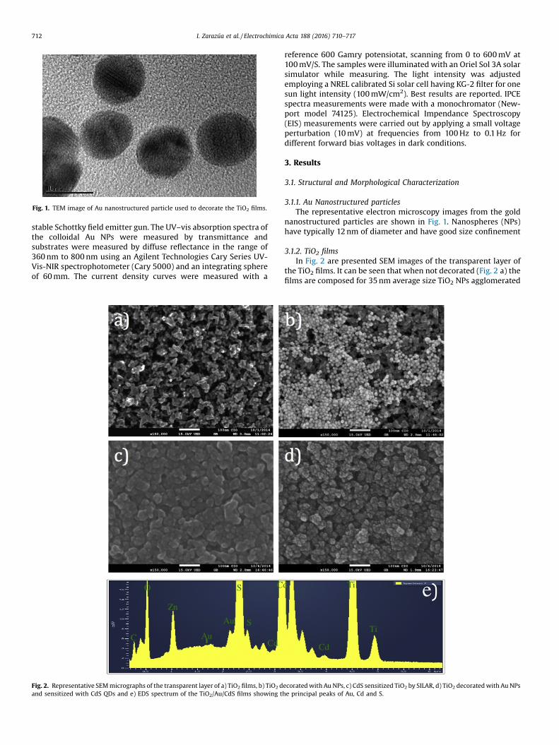
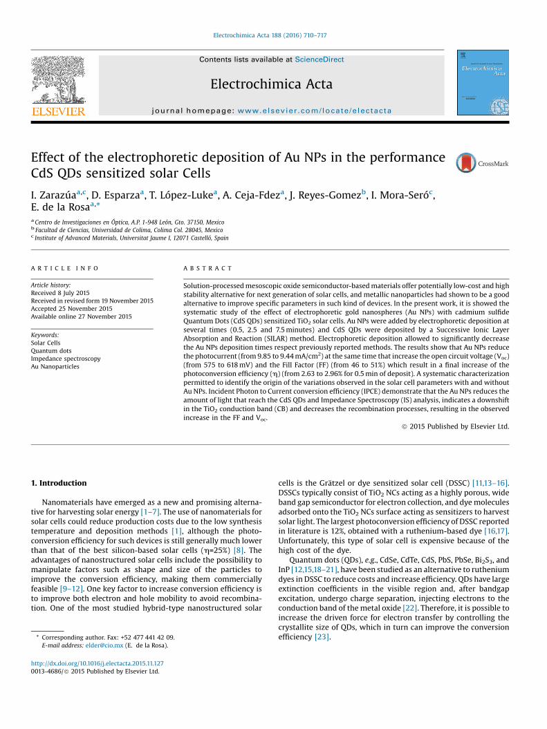
Fig. 1. TEM image of Au nanostructured particle used to decorate the TiO2 films.
712 I. Zarazúa et al. / Electrochimica Acta 188 (2016) 710–717
stable Schottky field emitter gun. The UV–vis absorption spectra ofthe colloidal Au NPs were measured by transmittance andsubstrates were measured by diffuse reflectance in the range of360 nm to 800 nm using an Agilent Technologies Cary Series UV-Vis-NIR spectrophotometer (Cary 5000) and an integrating sphereof 60 mm. The current density curves were measured with a
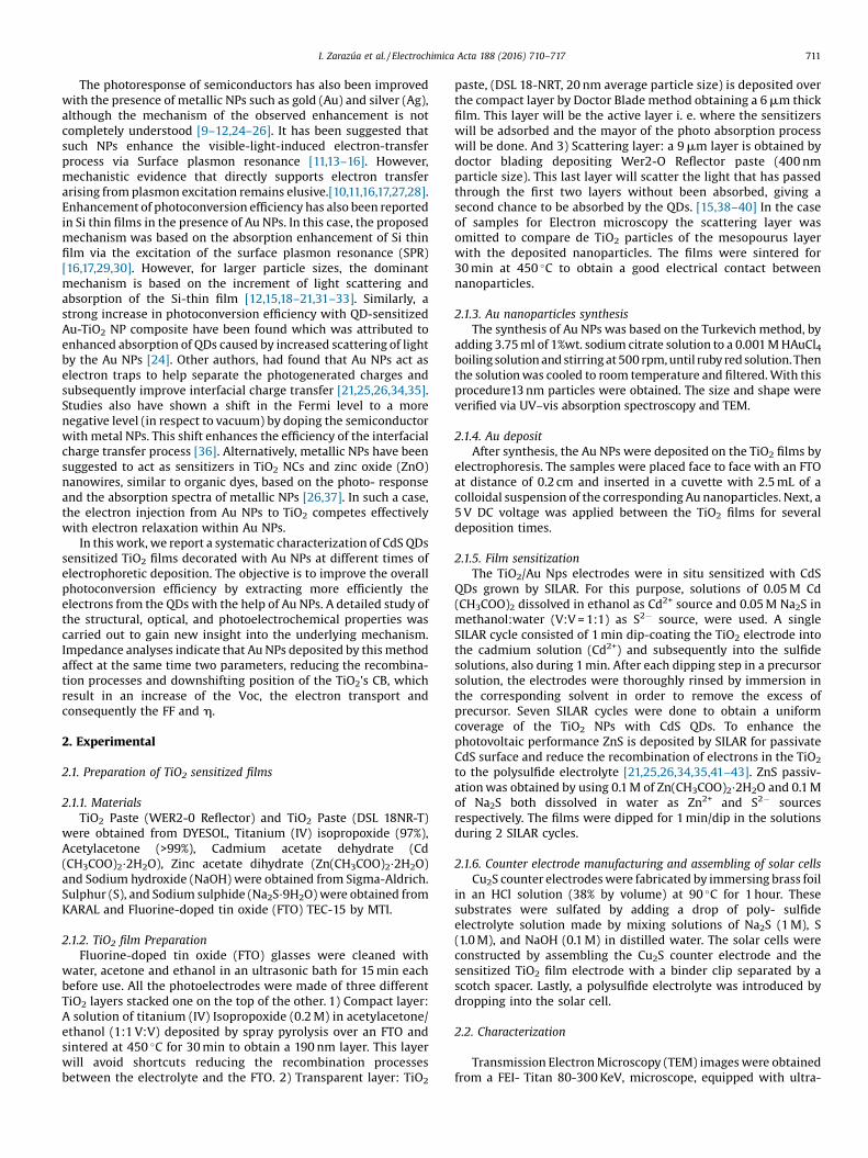
Fig. 2. Representative SEM micrographs of the transparent layer of a) TiO2 films, b) TiO2 dand sensitized with CdS QDs and e) EDS spectrum of the TiO2/Au/CdS films showing t
reference 600 Gamry potensiotat, scanning from 0 to 600 mV at100 mV/S. The samples were illuminated with an Oriel Sol 3A solarsimulator while measuring. The light intensity was adjustedemploying a NREL calibrated Si solar cell having KG-2 filter for onesun light intensity (100 mW/cm2). Best results are reported. IPCEspectra measurements were made with a monochromator (New-port model 74125). Electrochemical Impendance Spectroscopy(EIS) measurements were carried out by applying a small voltageperturbation (10 mV) at frequencies from 100 Hz to 0.1 Hz fordifferent forward bias voltages in dark conditions.
3. Results
3.1. Structural and Morphological Characterization
3.1.1. Au Nanostructured particlesThe representative electron microscopy images from the gold
nanostructured particles are shown in Fig. 1. Nanospheres (NPs)have typically 12 nm of diameter and have good size confinement
3.1.2. TiO2 filmsIn Fig. 2 are presented SEM images of the transparent layer of
the TiO2 films. It can be seen that when not decorated (Fig. 2 a) thefilms are composed for 35 nm average size TiO2 NPs agglomerated
ecorated with Au NPs, c) CdS sensitized TiO2 by SILAR, d) TiO2 decorated with Au NPshe principal peaks of Au, Cd and S.
, [nm]
Fig. 3. Representative absorption spectra of TiO2 films decorated with Au NPs andsensitized with CdS QDs. Showing the spectra of colloidal Au NPs.
I. Zarazúa et al. / Electrochimica Acta 188 (2016) 710–717 713
in a homogenous high porous arrangement. When Au NPs areelectrophoretic deposited (see Fig. 2 b), spherical particles ofapproximately 13 nm are observed on the film indifferently of thepolarity applied to the sample during the deposit. The size andshape of the nanoparticles indicate that they are Au NPs. Here alsocan be seen that the TiO2 NPs are not modified by theelectrophoresis. When the films are SILAR sensitized the TiO2
NPs are completely covered by the CdS QDs, partially filling thespaces between the particles. This gives the films a soft and lessporous appearance (see Fig. 2 c). Finally, when the films aredecorated with Au NPs and sensitized with CdS to form TiO2/Au/CdS samples (Fig. 2 d), a uniform coverage of the film with the QDsis obtained. But the appearance of the deposit is gnarled due to thepresence of the Au NPs. EDS analyses of the films (Fig. 2 e) confirmthe presence of the Au NPs and Cd and S from the QDs.
3.1.3. Optical AbsorptionThe absorption spectra of the Au NPs, bare TiO2 films, CdS QDs
sensitized TiO2 films, 2.5 minutes Au NPs electrophoretic decoratedfilms, Au decorated/CdS QDssensitizedTiO2films are shown in Fig. 3.The Au NPs absorption (red circles) presents a well-defined peak at519 nm that is consistent with the surface plasmon resonance (SPR)for such size of NPs. The TiO2 films (black solid line) have almost noabsorption in the visible region, rapidly increasing for wavelengths(l) lower than 400 nm. When Au NPs deposit is done for 2.5 min(orange +) there is a uniform increase in the absorption between380 and 800 nm, pointing to a light scattering effect. While, CdSsensitization of the TiO2 films (blue doted line) produces anabsorption shoulder from 400 to 500 nm, which corresponds tothe absorption of the CdS QDs[36,41,44]. Finally, when CdSsensitization is done in 2.5 min Au NPs decorated films, the shapein obtained spectra is similar to the films only sensitized with CdS
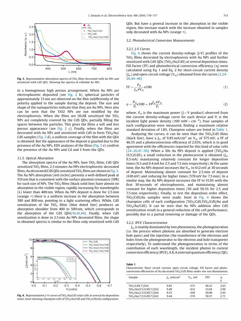
Fig. 4. Representative J–V curves of TiO2/Au/CdS solar cells at several Au depositiontimes. Inset showing champion cells of TiO2/Au/CdS and TiO2/CdS/Au configuration.
QDs. But have a general increase in the absorption in the visibleregion, this increase match with the increase obtained in samplesonly decorated with Au NPs (orange +).
3.2. Photoelectrical Conversion Measurements
3.2.1. J-V CurvesFig. 4 shows the current density-voltage (J-V) profiles of the
TiO2 films decorated by electrophoresis with Au NPs and furthersensitized with CdS QDs (TiO2/Au/CdS) at several deposition times.Fill Factor (FF) and photoelectrical conversion efficiency (h) werecalculated using Eq. 1 and Eq. 2 for short-circuit current density(Jsc) and open-circuit voltage (Voc) obtained from the curves [2,24–26,44–46]
FF ¼ Pm
JscxVocx100 ð1Þ
h ¼ Pm
Pix100 ¼ FF
JscxVoc
Pið2Þ
where, Pm is the maximum power (J � V product) observed fromthe current density-voltage curve for each device and Pi is theincident light power density (100 mW � cm�2). Four samples ofeach configuration were measured, finding a maximum relativestandard deviation of 1.8%. Champion values are listed in Table 1.
Analyzing the curves, it can be seen than the TiO2/CdS films(black line), have a Jsc of 9.85 mA/cm2 an Voc of 575 mV, a FF of46.5% and a photoconversion efficiency of 2.63%, which is in goodagreement with the efficiencies reported for this kind of solar cells[24–26,47–50]. When a 30s Au NPs deposit is applied (TiO2/Au(0.5)/CdS), a small reduction in the photocurrent is obtained (Jsc9.5 mA) maintaining relatively constant for longer depositiontimes (9.5 and 9.4 mA for 2.5 and 7.5 min respectively). At the sametime, the Au NPs deposit increases the Voc to 612 mV at 30 secondsof deposit. Maintaining almost constant for 2.5 min of deposit(618 mV) and reducing for higher times (570 mV for 7.5 min). In asimilar way, the Au NPs deposit increases the FF to 51.0% with thefirst 30 seconds of electrophoresis, and maintaining almostconstant for higher deposition times (50 and 50.3% for 2.5 and7.5 min respectively). Finally, to test the deposition order effect,TiO2/CdS/Au samples were made. Inset in Fig. 4 shows thechampion cells of each configuration (TiO2/CdS,TiO2/CdS/Au andTiO2/Au/CdS). It can be seen that Au NPs addition after CdSsensitization result in a general reduction of the cell performance,possibly due to a partial removing or damage of the QDs.
3.2.2. IPCE CharacterizationJsc is mainly dominated by two phenomena, the photogeneration
(i.e. the process where photons are absorbed to generate electronhole pairs) and the injection (the transference of the electrons andholes from the photogenerator to the electron and hole transporterrespectively). To understand the photogeneration in terms of thecontribution of each wavelength, the incident photon to currentconversion efficiency (IPCE), A.K.A.external quantum efficiency (QE),
Table 1Characteristic Short circuit current, open circuit voltage, Fill Factor and photo-conversion efficiencies of Au decorated TiO2/CdS films under one sun illumination.
Sample Jsc mA/cm2 Voc mV FF% h%
TiO2/CdS(7)/ZnS 9.85 -575 46.52 2.63TiO2/Au(0.5)/CdS(7)/ZnS 9.48 -612 51.04 2.96TiO2/Au(2.5)/CdS(7)/ZnS 9.53 �618 50.06 2.95TiO2/Au(7.5)/CdS(7)/ZnS 9.44 �570 50.37 2.71
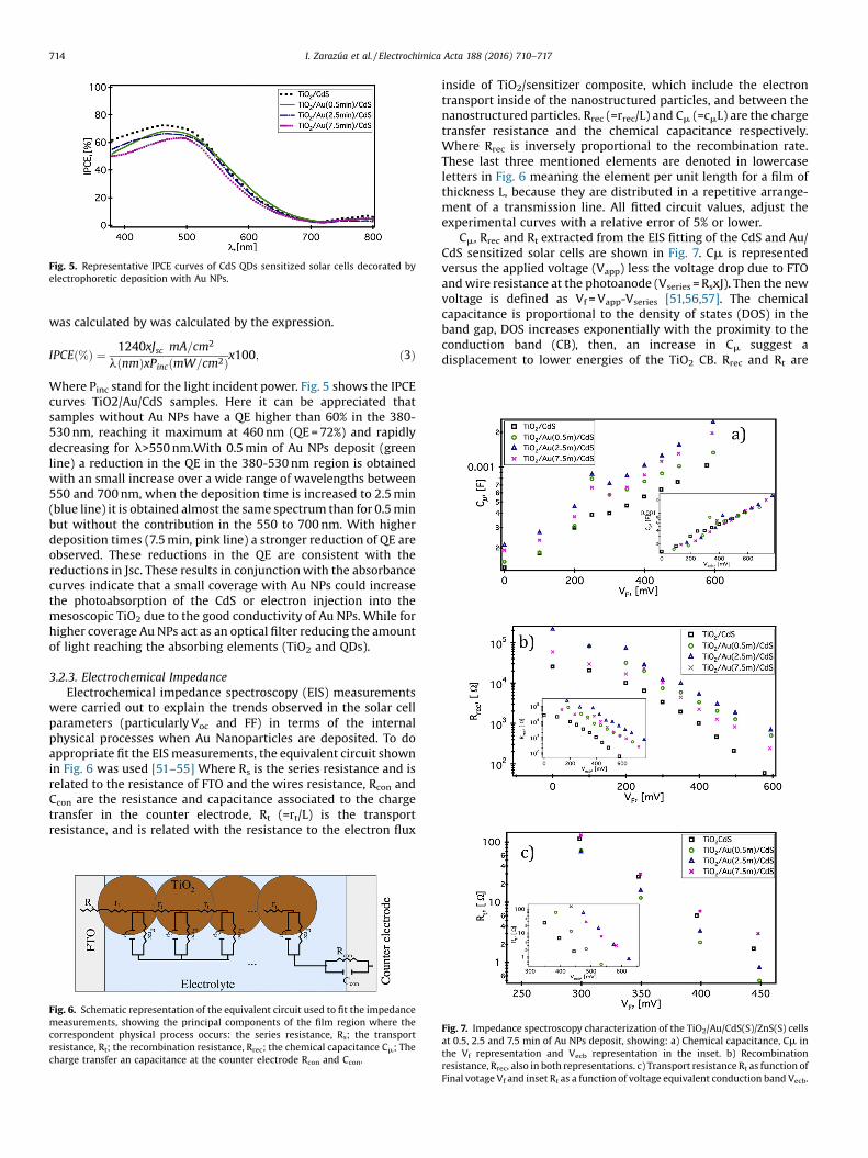
Fig. 5. Representative IPCE curves of CdS QDs sensitized solar cells decorated byelectrophoretic deposition with Au NPs.
714 I. Zarazúa et al. / Electrochimica Acta 188 (2016) 710–717
was calculated by was calculated by the expression.
IPCE %ð Þ ¼ 1240xJsc mA=cm2� �
l nmð ÞxPinc mW=cm2ð Þx100; ð3Þ
Where Pinc stand for the light incident power. Fig. 5 shows the IPCEcurves TiO2/Au/CdS samples. Here it can be appreciated thatsamples without Au NPs have a QE higher than 60% in the 380-530 nm, reaching it maximum at 460 nm (QE = 72%) and rapidlydecreasing for l>550 nm.With 0.5 min of Au NPs deposit (greenline) a reduction in the QE in the 380-530 nm region is obtainedwith an small increase over a wide range of wavelengths between550 and 700 nm, when the deposition time is increased to 2.5 min(blue line) it is obtained almost the same spectrum than for 0.5 minbut without the contribution in the 550 to 700 nm. With higherdeposition times (7.5 min, pink line) a stronger reduction of QE areobserved. These reductions in the QE are consistent with thereductions in Jsc. These results in conjunction with the absorbancecurves indicate that a small coverage with Au NPs could increasethe photoabsorption of the CdS or electron injection into themesoscopic TiO2 due to the good conductivity of Au NPs. While forhigher coverage Au NPs act as an optical filter reducing the amountof light reaching the absorbing elements (TiO2 and QDs).
3.2.3. Electrochemical ImpedanceElectrochemical impedance spectroscopy (EIS) measurements
were carried out to explain the trends observed in the solar cellparameters (particularly Voc and FF) in terms of the internalphysical processes when Au Nanoparticles are deposited. To doappropriate fit the EIS measurements, the equivalent circuit shownin Fig. 6 was used [51–55] Where Rs is the series resistance and isrelated to the resistance of FTO and the wires resistance, Rcon andCcon are the resistance and capacitance associated to the chargetransfer in the counter electrode, Rt (=rt/L) is the transportresistance, and is related with the resistance to the electron flux
Fig. 6. Schematic representation of the equivalent circuit used to fit the impedancemeasurements, showing the principal components of the film region where thecorrespondent physical process occurs: the series resistance, Rs; the transportresistance, Rt; the recombination resistance, Rrec; the chemical capacitance Cm; Thecharge transfer an capacitance at the counter electrode Rcon and Ccon.
inside of TiO2/sensitizer composite, which include the electrontransport inside of the nanostructured particles, and between thenanostructured particles. Rrec (=rrec/L) and Cm (=cmL) are the chargetransfer resistance and the chemical capacitance respectively.Where Rrec is inversely proportional to the recombination rate.These last three mentioned elements are denoted in lowercaseletters in Fig. 6 meaning the element per unit length for a film ofthickness L, because they are distributed in a repetitive arrange-ment of a transmission line. All fitted circuit values, adjust theexperimental curves with a relative error of 5% or lower.
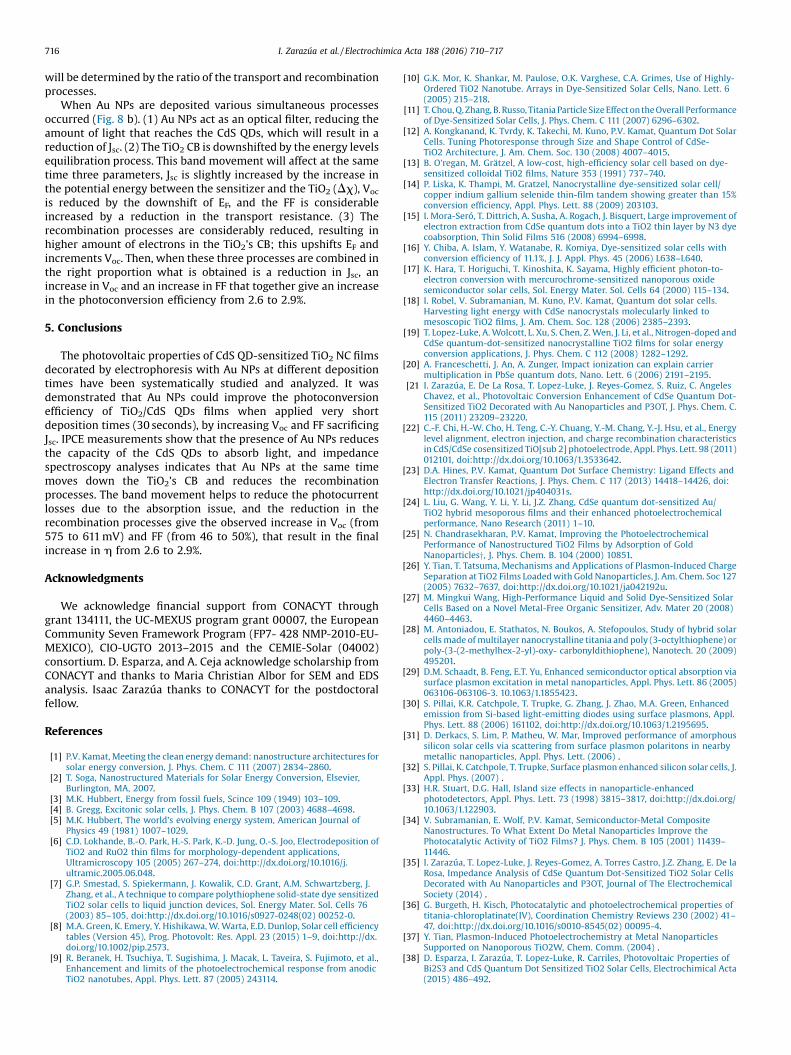
Cm, Rrec and Rt extracted from the EIS fitting of the CdS and Au/CdS sensitized solar cells are shown in Fig. 7. Cm is representedversus the applied voltage (Vapp) less the voltage drop due to FTOand wire resistance at the photoanode (Vseries = RsxJ). Then the newvoltage is defined as Vf = Vapp-Vseries [51,56,57]. The chemicalcapacitance is proportional to the density of states (DOS) in theband gap, DOS increases exponentially with the proximity to theconduction band (CB), then, an increase in Cm suggest adisplacement to lower energies of the TiO2 CB. Rrec and Rt are
Fig. 7. Impedance spectroscopy characterization of the TiO2/Au/CdS(S)/ZnS(S) cellsat 0.5, 2.5 and 7.5 min of Au NPs deposit, showing: a) Chemical capacitance, Cm inthe Vf representation and Vecb representation in the inset. b) Recombinationresistance, Rrec, also in both representations. c) Transport resistance Rt as function ofFinal votage Vf and inset Rt as a function of voltage equivalent conduction band Vecb.
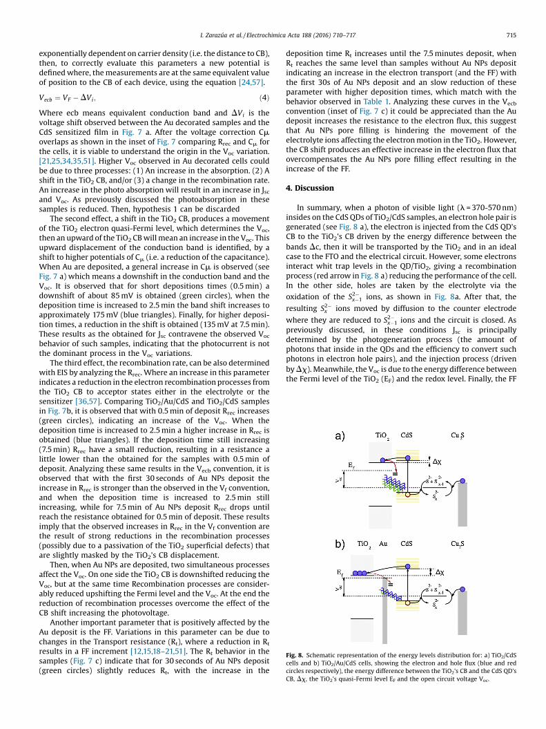
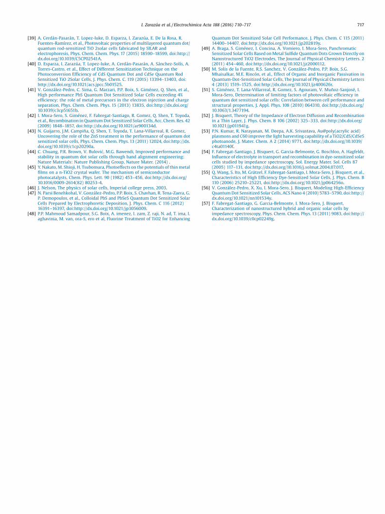
Fig. 8. Schematic representation of the energy levels distribution for: a) TiO2/CdScells and b) TiO2/Au/CdS cells, showing the electron and hole flux (blue and redcircles respectively), the energy difference between the TiO2's CB and the CdS QD's
I. Zarazúa et al. / Electrochimica Acta 188 (2016) 710–717 715
exponentially dependent on carrier density (i.e. the distance to CB),then, to correctly evaluate this parameters a new potential isdefined where, the measurements are at the same equivalent valueof position to the CB of each device, using the equation [24,57].
Vecb ¼ VF � DVi; ð4ÞWhere ecb means equivalent conduction band and DVi is thevoltage shift observed between the Au decorated samples and theCdS sensitized film in Fig. 7 a. After the voltage correction Cmoverlaps as shown in the inset of Fig. 7 comparing Rrec and Cm forthe cells, it is viable to understand the origin in the Voc variation.[21,25,34,35,51]. Higher Voc observed in Au decorated cells couldbe due to three processes: (1) An increase in the absorption. (2) Ashift in the TiO2 CB, and/or (3) a change in the recombination rate.An increase in the photo absorption will result in an increase in Jscand Voc. As previously discussed the photoabsorption in thesesamples is reduced. Then, hypothesis 1 can be discarded
The second effect, a shift in the TiO2 CB, produces a movementof the TiO2 electron quasi-Fermi level, which determines the Voc,then an upward of the TiO2 CB will mean an increase in the Voc. Thisupward displacement of the conduction band is identified, by ashift to higher potentials of Cm (i.e. a reduction of the capacitance).When Au are deposited, a general increase in Cm is observed (seeFig. 7 a) which means a downshift in the conduction band and theVoc. It is observed that for short depositions times (0.5 min) adownshift of about 85 mV is obtained (green circles), when thedeposition time is increased to 2.5 min the band shift increases toapproximately 175 mV (blue triangles). Finally, for higher deposi-tion times, a reduction in the shift is obtained (135 mV at 7.5 min).These results as the obtained for Jsc contravene the observed Voc
behavior of such samples, indicating that the photocurrent is notthe dominant process in the Voc variations.
The third effect, the recombination rate, can be also determinedwith EIS by analyzing the Rrec. Where an increase in this parameterindicates a reduction in the electron recombination processes fromthe TiO2 CB to acceptor states either in the electrolyte or thesensitizer [36,57]. Comparing TiO2/Au/CdS and TiO2/CdS samplesin Fig. 7b, it is observed that with 0.5 min of deposit Rrec increases(green circles), indicating an increase of the Voc. When thedeposition time is increased to 2.5 min a higher increase in Rrec isobtained (blue triangles). If the deposition time still increasing(7.5 min) Rrec have a small reduction, resulting in a resistance alittle lower than the obtained for the samples with 0.5 min ofdeposit. Analyzing these same results in the Vecb convention, it isobserved that with the first 30 seconds of Au NPs deposit theincrease in Rrec is stronger than the observed in the Vf convention,and when the deposition time is increased to 2.5 min stillincreasing, while for 7.5 min of Au NPs deposit Rrec drops untilreach the resistance obtained for 0.5 min of deposit. These resultsimply that the observed increases in Rrec in the Vf convention arethe result of strong reductions in the recombination processes(possibly due to a passivation of the TiO2 superficial defects) thatare slightly masked by the TiO2's CB displacement.
Then, when Au NPs are deposited, two simultaneous processesaffect the Voc. On one side the TiO2 CB is downshifted reducing theVoc, but at the same time Recombination processes are consider-ably reduced upshifting the Fermi level and the Voc. At the end thereduction of recombination processes overcome the effect of theCB shift increasing the photovoltage.
Another important parameter that is positively affected by theAu deposit is the FF. Variations in this parameter can be due tochanges in the Transport resistance (Rt), where a reduction in Rt
results in a FF increment [12,15,18–21,51]. The Rt behavior in thesamples (Fig. 7 c) indicate that for 30 seconds of Au NPs deposit(green circles) slightly reduces Rt, with the increase in the
deposition time Rt increases until the 7.5 minutes deposit, whenRt reaches the same level than samples without Au NPs depositindicating an increase in the electron transport (and the FF) withthe first 30s of Au NPs deposit and an slow reduction of theseparameter with higher deposition times, which match with thebehavior observed in Table 1. Analyzing these curves in the Vecb
convention (inset of Fig. 7 c) it could be appreciated than the Audeposit increases the resistance to the electron flux, this suggestthat Au NPs pore filling is hindering the movement of theelectrolyte ions affecting the electron motion in the TiO2. However,the CB shift produces an effective increase in the electron flux thatovercompensates the Au NPs pore filling effect resulting in theincrease of the FF.
4. Discussion
In summary, when a photon of visible light (l = 370-570 nm)insides on the CdS QDs of TiO2/CdS samples, an electron hole pair isgenerated (see Fig. 8 a), the electron is injected from the CdS QD'sCB to the TiO2's CB driven by the energy difference between thebands Dc, then it will be transported by the TiO2 and in an idealcase to the FTO and the electrical circuit. However, some electronsinteract whit trap levels in the QD/TiO2, giving a recombinationprocess (red arrow in Fig. 8 a) reducing the performance of the cell.In the other side, holes are taken by the electrolyte via the
oxidation of the S2�x�1 ions, as shown in Fig. 8a. After that, the
resulting S2�x ions moved by diffusion to the counter electrode
where they are reduced to S2�x�1 ions and the circuit is closed. Aspreviously discussed, in these conditions Jsc is principallydetermined by the photogeneration process (the amount ofphotons that inside in the QDs and the efficiency to convert suchphotons in electron hole pairs), and the injection process (drivenby Dx). Meanwhile, the Voc is due to the energy difference betweenthe Fermi level of the TiO2 (EF) and the redox level. Finally, the FF
CB, Dx, the TiO2's quasi-Fermi level EF and the open circuit voltage Voc.
716 I. Zarazúa et al. / Electrochimica Acta 188 (2016) 710–717
will be determined by the ratio of the transport and recombinationprocesses.
When Au NPs are deposited various simultaneous processesoccurred (Fig. 8 b). (1) Au NPs act as an optical filter, reducing theamount of light that reaches the CdS QDs, which will result in areduction of Jsc. (2) The TiO2 CB is downshifted by the energy levelsequilibration process. This band movement will affect at the sametime three parameters, Jsc is slightly increased by the increase inthe potential energy between the sensitizer and the TiO2 (Dx), Voc
is reduced by the downshift of EF, and the FF is considerableincreased by a reduction in the transport resistance. (3) Therecombination processes are considerably reduced, resulting inhigher amount of electrons in the TiO2's CB; this upshifts EF andincrements Voc. Then, when these three processes are combined inthe right proportion what is obtained is a reduction in Jsc, anincrease in Voc and an increase in FF that together give an increasein the photoconversion efficiency from 2.6 to 2.9%.
5. Conclusions
The photovoltaic properties of CdS QD-sensitized TiO2 NC filmsdecorated by electrophoresis with Au NPs at different depositiontimes have been systematically studied and analyzed. It wasdemonstrated that Au NPs could improve the photoconversionefficiency of TiO2/CdS QDs films when applied very shortdeposition times (30 seconds), by increasing Voc and FF sacrificingJsc. IPCE measurements show that the presence of Au NPs reducesthe capacity of the CdS QDs to absorb light, and impedancespectroscopy analyses indicates that Au NPs at the same timemoves down the TiO2's CB and reduces the recombinationprocesses. The band movement helps to reduce the photocurrentlosses due to the absorption issue, and the reduction in therecombination processes give the observed increase in Voc (from575 to 611 mV) and FF (from 46 to 50%), that result in the finalincrease in h from 2.6 to 2.9%.
Acknowledgments
We acknowledge financial support from CONACYT throughgrant 134111, the UC-MEXUS program grant 00007, the EuropeanCommunity Seven Framework Program (FP7- 428 NMP-2010-EU-MEXICO), CIO-UGTO 2013–2015 and the CEMIE-Solar (04002)consortium. D. Esparza, and A. Ceja acknowledge scholarship fromCONACYT and thanks to Maria Christian Albor for SEM and EDSanalysis. Isaac Zarazúa thanks to CONACYT for the postdoctoralfellow.
References
[1] P.V. Kamat, Meeting the clean energy demand: nanostructure architectures forsolar energy conversion, J. Phys. Chem. C 111 (2007) 2834–2860.
[2] T. Soga, Nanostructured Materials for Solar Energy Conversion, Elsevier,Burlington, MA, 2007.
[3] M.K. Hubbert, Energy from fossil fuels, Scince 109 (1949) 103–109.[4] B. Gregg, Excitonic solar cells, J. Phys. Chem. B 107 (2003) 4688–4698.[5] M.K. Hubbert, The world's evolving energy system, American Journal of
Physics 49 (1981) 1007–1029.[6] C.D. Lokhande, B.-O. Park, H.-S. Park, K.-D. Jung, O.-S. Joo, Electrodeposition of
TiO2 and RuO2 thin films for morphology-dependent applications,Ultramicroscopy 105 (2005) 267–274, doi:http://dx.doi.org/10.1016/j.ultramic.2005.06.048.
[7] G.P. Smestad, S. Spiekermann, J. Kowalik, C.D. Grant, A.M. Schwartzberg, J.Zhang, et al., A technique to compare polythiophene solid-state dye sensitizedTiO2 solar cells to liquid junction devices, Sol. Energy Mater. Sol. Cells 76(2003) 85–105, doi:http://dx.doi.org/10.1016/s0927-0248(02) 00252-0.
[8] M.A. Green, K. Emery, Y. Hishikawa, W. Warta, E.D. Dunlop, Solar cell efficiencytables (Version 45), Prog. Photovolt: Res. Appl. 23 (2015) 1–9, doi:http://dx.doi.org/10.1002/pip.2573.
[9] R. Beranek, H. Tsuchiya, T. Sugishima, J. Macak, L. Taveira, S. Fujimoto, et al.,Enhancement and limits of the photoelectrochemical response from anodicTiO2 nanotubes, Appl. Phys. Lett. 87 (2005) 243114.
[10] G.K. Mor, K. Shankar, M. Paulose, O.K. Varghese, C.A. Grimes, Use of Highly-Ordered TiO2 Nanotube. Arrays in Dye-Sensitized Solar Cells, Nano. Lett. 6(2005) 215–218.
[11] T. Chou, Q. Zhang, B. Russo, Titania Particle Size Effect on the Overall Performanceof Dye-Sensitized Solar Cells, J. Phys. Chem. C 111 (2007) 6296–6302.
[12] A. Kongkanand, K. Tvrdy, K. Takechi, M. Kuno, P.V. Kamat, Quantum Dot SolarCells. Tuning Photoresponse through Size and Shape Control of CdSe-TiO2 Architecture, J. Am. Chem. Soc. 130 (2008) 4007–4015.
[13] B. O'regan, M. Grätzel, A low-cost, high-efficiency solar cell based on dye-sensitized colloidal Ti02 films, Nature 353 (1991) 737–740.
[14] P. Liska, K. Thampi, M. Gratzel, Nanocrystalline dye-sensitized solar cell/copper indium gallium selenide thin-film tandem showing greater than 15%conversion efficiency, Appl. Phys. Lett. 88 (2009) 203103.
[15] I. Mora-Seró, T. Dittrich, A. Susha, A. Rogach, J. Bisquert, Large improvement ofelectron extraction from CdSe quantum dots into a TiO2 thin layer by N3 dyecoabsorption, Thin Solid Films 516 (2008) 6994–6998.
[16] Y. Chiba, A. Islam, Y. Watanabe, R. Komiya, Dye-sensitized solar cells withconversion efficiency of 11.1%, J. J. Appl. Phys. 45 (2006) L638–L640.
[17] K. Hara, T. Horiguchi, T. Kinoshita, K. Sayama, Highly efficient photon-to-electron conversion with mercurochrome-sensitized nanoporous oxidesemiconductor solar cells, Sol. Energy Mater. Sol. Cells 64 (2000) 115–134.
[18] I. Robel, V. Subramanian, M. Kuno, P.V. Kamat, Quantum dot solar cells.Harvesting light energy with CdSe nanocrystals molecularly linked tomesoscopic TiO2 films, J. Am. Chem. Soc. 128 (2006) 2385–2393.
[19] T. Lopez-Luke, A. Wolcott, L. Xu, S. Chen, Z. Wen, J. Li, et al., Nitrogen-doped andCdSe quantum-dot-sensitized nanocrystalline TiO2 films for solar energyconversion applications, J. Phys. Chem. C 112 (2008) 1282–1292.
[20] A. Franceschetti, J. An, A. Zunger, Impact ionization can explain carriermultiplication in PbSe quantum dots, Nano. Lett. 6 (2006) 2191–2195.
[21 I. Zarazúa, E. De La Rosa, T. Lopez-Luke, J. Reyes-Gomez, S. Ruiz, C. AngelesChavez, et al., Photovoltaic Conversion Enhancement of CdSe Quantum Dot-Sensitized TiO2 Decorated with Au Nanoparticles and P3OT, J. Phys. Chem. C.115 (2011) 23209–23220.
[22] C.-F. Chi, H.-W. Cho, H. Teng, C.-Y. Chuang, Y.-M. Chang, Y.-J. Hsu, et al., Energylevel alignment, electron injection, and charge recombination characteristicsin CdS/CdSe cosensitized TiO[sub 2] photoelectrode, Appl. Phys. Lett. 98 (2011)012101, doi:http://dx.doi.org/10.1063/1.3533642.
[23] D.A. Hines, P.V. Kamat, Quantum Dot Surface Chemistry: Ligand Effects andElectron Transfer Reactions, J. Phys. Chem. C 117 (2013) 14418–14426, doi:http://dx.doi.org/10.1021/jp404031s.
[24] L. Liu, G. Wang, Y. Li, Y. Li, J.Z. Zhang, CdSe quantum dot-sensitized Au/TiO2 hybrid mesoporous films and their enhanced photoelectrochemicalperformance, Nano Research (2011) 1–10.
[25] N. Chandrasekharan, P.V. Kamat, Improving the PhotoelectrochemicalPerformance of Nanostructured TiO2 Films by Adsorption of GoldNanoparticlesy, J. Phys. Chem. B. 104 (2000) 10851.
[26] Y. Tian, T. Tatsuma, Mechanisms and Applications of Plasmon-Induced ChargeSeparation at TiO2 Films Loaded with Gold Nanoparticles, J. Am. Chem. Soc 127(2005) 7632–7637, doi:http://dx.doi.org/10.1021/ja042192u.
[27] M. Mingkui Wang, High-Performance Liquid and Solid Dye-Sensitized SolarCells Based on a Novel Metal-Free Organic Sensitizer, Adv. Mater 20 (2008)4460–4463.
[28] M. Antoniadou, E. Stathatos, N. Boukos, A. Stefopoulos, Study of hybrid solarcells made of multilayer nanocrystalline titania and poly (3-octylthiophene) orpoly-(3-(2-methylhex-2-yl)-oxy- carbonyldithiophene), Nanotech. 20 (2009)495201.
[29] D.M. Schaadt, B. Feng, E.T. Yu, Enhanced semiconductor optical absorption viasurface plasmon excitation in metal nanoparticles, Appl. Phys. Lett. 86 (2005)063106-063106-3. 10.1063/1.1855423.
[30] S. Pillai, K.R. Catchpole, T. Trupke, G. Zhang, J. Zhao, M.A. Green, Enhancedemission from Si-based light-emitting diodes using surface plasmons, Appl.Phys. Lett. 88 (2006) 161102, doi:http://dx.doi.org/10.1063/1.2195695.
[31] D. Derkacs, S. Lim, P. Matheu, W. Mar, Improved performance of amorphoussilicon solar cells via scattering from surface plasmon polaritons in nearbymetallic nanoparticles, Appl. Phys. Lett. (2006) .
[32] S. Pillai, K. Catchpole, T. Trupke, Surface plasmon enhanced silicon solar cells, J.Appl. Phys. (2007) .
[33] H.R. Stuart, D.G. Hall, Island size effects in nanoparticle-enhancedphotodetectors, Appl. Phys. Lett. 73 (1998) 3815–3817, doi:http://dx.doi.org/10.1063/1.122903.
[34] V. Subramanian, E. Wolf, P.V. Kamat, Semiconductor-Metal CompositeNanostructures. To What Extent Do Metal Nanoparticles Improve thePhotocatalytic Activity of TiO2 Films? J. Phys. Chem. B 105 (2001) 11439–11446.
[35] I. Zarazúa, T. Lopez-Luke, J. Reyes-Gomez, A. Torres Castro, J.Z. Zhang, E. De laRosa, Impedance Analysis of CdSe Quantum Dot-Sensitized TiO2 Solar CellsDecorated with Au Nanoparticles and P3OT, Journal of The ElectrochemicalSociety (2014) .
[36] G. Burgeth, H. Kisch, Photocatalytic and photoelectrochemical properties oftitania-chloroplatinate(IV), Coordination Chemistry Reviews 230 (2002) 41–47, doi:http://dx.doi.org/10.1016/s0010-8545(02) 00095-4.
[37] Y. Tian, Plasmon-Induced Photoelectrochemistry at Metal NanoparticlesSupported on Nanoporous TiO2W, Chem. Comm. (2004) .
[38] D. Esparza, I. Zarazúa, T. Lopez-Luke, R. Carriles, Photovoltaic Properties ofBi2S3 and CdS Quantum Dot Sensitized TiO2 Solar Cells, Electrochimical Acta(2015) 486–492.
I. Zarazúa et al. / Electrochimica Acta 188 (2016) 710–717 717
[39] A. Cerdán-Pasarán, T. Lopez-luke, D. Esparza, I. Zarazúa, E. De la Rosa, R.Fuentes-Ramírez, et al., Photovoltaic properties of multilayered quantum dot/quantum rod-sensitized TiO 2solar cells fabricated by SILAR andelectrophoresis, Phys. Chem. Chem. Phys. 17 (2015) 18590–18599, doi:http://dx.doi.org/10.1039/C5CP02541A.
[40] D. Esparza, I. Zarazúa, T. Lopez-luke, A. Cerdán-Pasarán, A. Sánchez-Solís, A.Torres-Castro, et al., Effect of Different Sensitization Technique on thePhotoconversion Efficiency of CdS Quantum Dot and CdSe Quantum RodSensitized TiO 2Solar Cells, J. Phys. Chem. C. 119 (2015) 13394–13403, doi:http://dx.doi.org/10.1021/acs.jpcc.5b01525.
[41] V. González-Pedro, C. Sima, G. Marzari, P.P. Boix, S. Giménez, Q. Shen, et al.,High performance PbS Quantum Dot Sensitized Solar Cells exceeding 4%efficiency: the role of metal precursors in the electron injection and chargeseparation, Phys. Chem. Chem. Phys. 15 (2013) 13835, doi:http://dx.doi.org/10.1039/c3cp51651b.
[42] I. Mora-Sero, S. Giménez, F. Fabregat-Santiago, R. Gomez, Q. Shen, T. Toyoda,et al., Recombination in Quantum Dot Sensitized Solar Cells, Acc. Chem. Res. 42(2009) 1848–1857, doi:http://dx.doi.org/10.1021/ar900134d.
[43] N. Guijarro, J.M. Campiña, Q. Shen, T. Toyoda, T. Lana-Villarreal, R. Gomez,Uncovering the role of the ZnS treatment in the performance of quantum dotsensitized solar cells, Phys. Chem. Chem. Phys. 13 (2011) 12024, doi:http://dx.doi.org/10.1039/c1cp20290a.
[44] C. Chuang, P.R. Brown, V. Bulovi�c, M.G. Bawendi, Improved performance andstability in quantum dot solar cells through band alignment engineering:Nature Materials: Nature Publishing Group, Nature Mater. (2014) .
[45] Y. Nakato, M. Shioji, H. Tsubomura, Photoeffects on the potentials of thin metalfilms on a n-TiO2 crystal wafer. The mechanism of semiconductorphotocatalysts, Chem. Phys. Lett. 90 (1982) 453–456, doi:http://dx.doi.org/10.1016/0009-2614(82) 80253-4.
[46] J. Nelson, The physics of solar cells, Imperial college press, 2003.[47] N. Parsi Benehkohal, V. González-Pedro, P.P. Boix, S. Chavhan, R. Tena-Zaera, G.
P. Demopoulos, et al., Colloidal PbS and PbSeS Quantum Dot Sensitized SolarCells Prepared by Electrophoretic Deposition, J. Phys. Chem. C 116 (2012)16391–16397, doi:http://dx.doi.org/10.1021/jp3056009.
[48] P.P. Mahmoud Samadpour, S.G. Boix, A. imenez, I. zam, Z. raji, N. ad, T. ima, I.aghavinia, M. van, ora-S, ero et al, Fluorine Treatment of TiO2 for Enhancing
Quantum Dot Sensitized Solar Cell Performance, J. Phys. Chem. C 115 (2011)14400–14407, doi:http://dx.doi.org/10.1021/jp202819y.
[49] A. Braga, S. Giménez, I. Concina, A. Vomiero, I. Mora-Sero, PanchromaticSensitized Solar Cells Based on Metal Sulfide Quantum Dots Grown Directly onNanostructured TiO2 Electrodes, The Journal of Physical Chemistry Letters. 2(2011) 454–460, doi:http://dx.doi.org/10.1021/jz2000112.
[50] M. Solis de la Fuente, R.S. Sanchez, V. González-Pedro, P.P. Boix, S.G.Mhaisalkar, M.E. Rincón, et al., Effect of Organic and Inorganic Passivation inQuantum-Dot-Sensitized Solar Cells, The Journal of Physical Chemistry Letters4 (2013) 1519–1525, doi:http://dx.doi.org/10.1021/jz400626r.
[51] S. Giménez, T. Lana-Villarreal, R. Gomez, S. Agouram, V. Muñoz-Sanjosé, I.Mora-Sero, Determination of limiting factors of photovoltaic efficiency inquantum dot sensitized solar cells: Correlation between cell performance andstructural properties, J. Appl. Phys. 108 (2010) 064310, doi:http://dx.doi.org/10.1063/1.3477194.
[52] J. Bisquert, Theory of the Impedance of Electron Diffusion and Recombinationin a Thin Layer, J. Phys. Chem. B 106 (2002) 325–333, doi:http://dx.doi.org/10.1021/jp011941g.
[53] P.N. Kumar, R. Narayanan, M. Deepa, A.K. Srivastava, Au@poly(acrylic acid)plasmons and C60 improve the light harvesting capability of a TiO2/CdS/CdSeSphotoanode, J. Mater. Chem. A 2 (2014) 9771, doi:http://dx.doi.org/10.1039/c4ta01140f.
[54] F. Fabregat-Santiago, J. Bisquert, G. Garcia-Belmonte, G. Boschloo, A. Hagfeldt,Influence of electrolyte in transport and recombination in dye-sensitized solarcells studied by impedance spectroscopy, Sol. Energy Mater. Sol. Cells 87(2005) 117–131, doi:http://dx.doi.org/10.1016/j.solmat.2004.07.017.
[55] Q. Wang, S. Ito, M. Grätzel, F. Fabregat-Santiago, I. Mora-Sero, J. Bisquert, et al.,Characteristics of High Efficiency Dye-Sensitized Solar Cells, J. Phys. Chem. B110 (2006) 25210–25221, doi:http://dx.doi.org/10.1021/jp064256o.
[56] V. González-Pedro, X. Xu, I. Mora-Sero, J. Bisquert, Modeling High-EfficiencyQuantum Dot Sensitized Solar Cells, ACS Nano 4 (2010) 5783–5790, doi:http://dx.doi.org/10.1021/nn101534y.
[57] F. Fabregat-Santiago, G. Garcia-Belmonte, I. Mora-Sero, J. Bisquert,Characterization of nanostructured hybrid and organic solar cells byimpedance spectroscopy, Phys. Chem. Chem. Phys. 13 (2011) 9083, doi:http://dx.doi.org/10.1039/c0cp02249g.