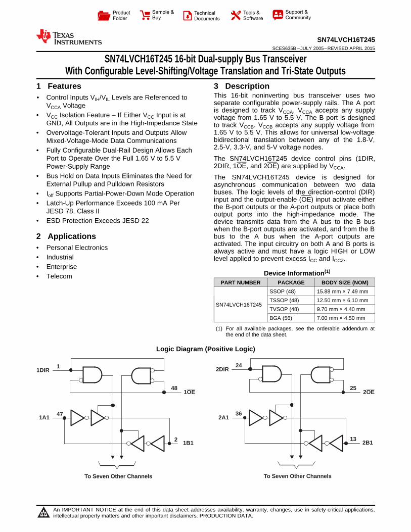
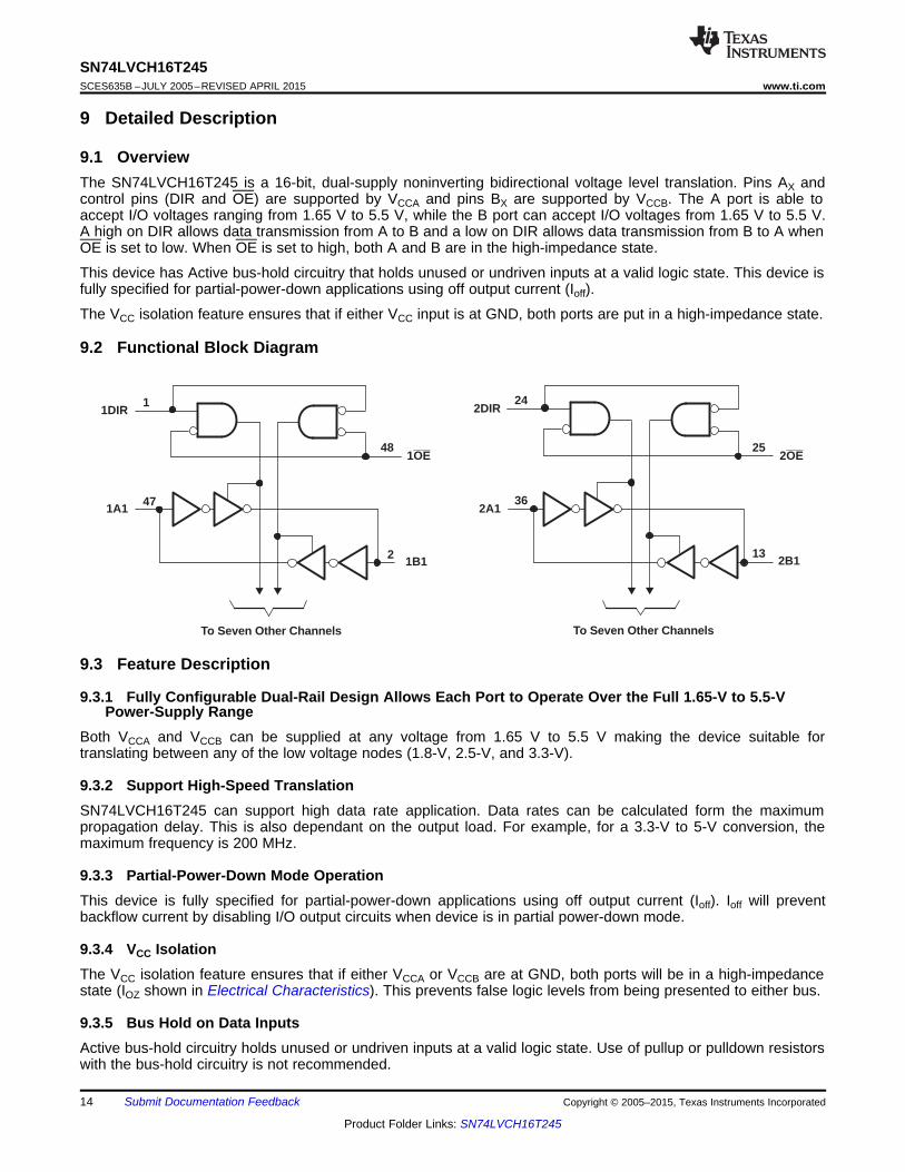
To Seven Other Channels
1DIR
1A1
1B1
1OE
To Seven Other Channels
2DIR
2A1
2B1
2OE
1
47
24
36
48
2
25
13
Product
Folder
Sample &Buy
Technical
Documents
Tools &
Software
Support &Community
SN74LVCH16T245SCES635B –JULY 2005–REVISED APRIL 2015
SN74LVCH16T245 16-bit Dual-supply Bus TransceiverWith Configurable Level-Shifting/Voltage Translation and Tri-State Outputs
1 Features 3 DescriptionThis 16-bit noninverting bus transceiver uses two
1• Control Inputs VIH/VIL Levels are Referenced toseparate configurable power-supply rails. The A portVCCA Voltageis designed to track VCCA. VCCA accepts any supply
• VCC Isolation Feature – If Either VCC Input is at voltage from 1.65 V to 5.5 V. The B port is designedGND, All Outputs are in the High-Impedance State to track VCCB. VCCB accepts any supply voltage from
1.65 V to 5.5 V. This allows for universal low-voltage• Overvoltage-Tolerant Inputs and Outputs Allowbidirectional translation between any of the 1.8-V,Mixed-Voltage-Mode Data Communications2.5-V, 3.3-V, and 5-V voltage nodes.• Fully Configurable Dual-Rail Design Allows Each
Port to Operate Over the Full 1.65 V to 5.5 V The SN74LVCH16T245 device control pins (1DIR,2DIR, 1OE, and 2OE) are supplied by VCCA.Power-Supply Range
• Bus Hold on Data Inputs Eliminates the Need for The SN74LVCH16T245 device is designed forExternal Pullup and Pulldown Resistors asynchronous communication between two data
buses. The logic levels of the direction-control (DIR)• Ioff Supports Partial-Power-Down Mode Operationinput and the output-enable (OE) input activate either• Latch-Up Performance Exceeds 100 mA Per the B-port outputs or the A-port outputs or place bothJESD 78, Class II output ports into the high-impedance mode. The
• ESD Protection Exceeds JESD 22 device transmits data from the A bus to the B buswhen the B-port outputs are activated, and from the Bbus to the A bus when the A-port outputs are2 Applicationsactivated. The input circuitry on both A and B ports is• Personal Electronics always active and must have a logic HIGH or LOW
• Industrial level applied to prevent excess ICC and ICCZ.• Enterprise
Device Information(1)• Telecom
PART NUMBER PACKAGE BODY SIZE (NOM)SSOP (48) 15.88 mm × 7.49 mmTSSOP (48) 12.50 mm × 6.10 mm
SN74LVCH16T245TVSOP (48) 9.70 mm × 4.40 mmBGA (56) 7.00 mm × 4.50 mm
(1) For all available packages, see the orderable addendum atthe end of the data sheet.
Logic Diagram (Positive Logic)
1
An IMPORTANT NOTICE at the end of this data sheet addresses availability, warranty, changes, use in safety-critical applications,intellectual property matters and other important disclaimers. PRODUCTION DATA.
SN74LVCH16T245SCES635B –JULY 2005–REVISED APRIL 2015 www.ti.com
Table of Contents1 Features .................................................................. 1 9 Detailed Description ............................................ 14
9.1 Overview ................................................................. 142 Applications ........................................................... 19.2 Functional Block Diagram ....................................... 143 Description ............................................................. 19.3 Feature Description................................................. 144 Revision History..................................................... 29.4 Device Functional Modes........................................ 155 Description (continued)......................................... 3
10 Application and Implementation........................ 166 Pin Configuration and Functions ......................... 410.1 Application Information.......................................... 167 Specifications......................................................... 610.2 Typical Application ............................................... 177.1 Absolute Maximum Ratings ..................................... 6
11 Power Supply Recommendations ..................... 197.2 ESD Ratings.............................................................. 612 Layout................................................................... 197.3 Recommended Operating Conditions ...................... 7
12.1 Layout Guidelines ................................................. 197.4 Thermal Information .................................................. 812.2 Layout Example .................................................... 207.5 Electrical Characteristics........................................... 8
13 Device and Documentation Support ................. 217.6 Switching Characteristics for VCCA = 1.8 V ±0.15 V . 913.1 Documentation Support ........................................ 217.7 Switching Characteristics for VCCA = 2.5 V ±0.2 V . 1013.2 Trademarks ........................................................... 217.8 Switching Characteristics for VCCA = 3.3 V ±0.3 V . 1013.3 Electrostatic Discharge Caution............................ 217.9 Switching Characteristics for VCCA = 5 V ±0.5 V .... 1113.4 Glossary ................................................................ 217.10 Operating Characteristics...................................... 11
14 Mechanical, Packaging, and Orderable7.11 Typical Characteristics .......................................... 12Information ........................................................... 218 Parameter Measurement Information ................ 13
4 Revision History
Changes from Revision A (August 2005) to Revision B Page
• Added Pin Configuration and Functions section, ESD Ratings table, Feature Description section, Device FunctionalModes, Application and Implementation section, Power Supply Recommendations section, Layout section, Deviceand Documentation Support section, and Mechanical, Packaging, and Orderable Information section .............................. 1
2 Submit Documentation Feedback Copyright © 2005–2015, Texas Instruments Incorporated
Product Folder Links: SN74LVCH16T245
SN74LVCH16T245www.ti.com SCES635B –JULY 2005–REVISED APRIL 2015
5 Description (continued)Active bus-hold circuitry holds unused or undriven data inputs at a valid logic state. Use of pullup or pulldownresistors with the bus-hold circuitry is not recommended. The bus-hold circuitry on the powered-up side alwaysstays active.
This device is fully specified for partial-power-down applications using Ioff. The Ioff circuitry disables the outputs,preventing damaging current backflow through the device when it is powered down.
The VCC isolation feature ensures that if either VCC input is at GND, then all outputs are in the high-impedancestate. To ensure the high-impedance state during power up or power down, OE should be tied to VCC through apullup resistor; the minimum value of the resistor is determined by the current-sinking capability of the driver.
Copyright © 2005–2015, Texas Instruments Incorporated Submit Documentation Feedback 3
Product Folder Links: SN74LVCH16T245
1
2
3
4
5
6
7
8
9
10
11
12
13
14
15
16
17
18
19
20
21
22
23
24
48
47
46
45
44
43
42
41
40
39
38
37
36
35
34
33
32
31
30
29
28
27
26
25
1DIR
1B1
1B2
GND
1B3
1B4
VCCB
1B5
1B6
GND
1B7
1B8
2B1
2B2
GND
2B3
2B4
VCCB
2B5
2B6
GND
2B7
2B8
2DIR
1OE
1A1
1A2
GND
1A3
1A4
VCCA
1A5
1A6
GND
1A7
1A8
2A1
2A2
GND
2A3
2A4
VCCA
2A5
2A6
GND
2A7
2A8
2OE
J
H
G
F
E
D
C
B
A
21 3 4 65
K
SN74LVCH16T245SCES635B –JULY 2005–REVISED APRIL 2015 www.ti.com
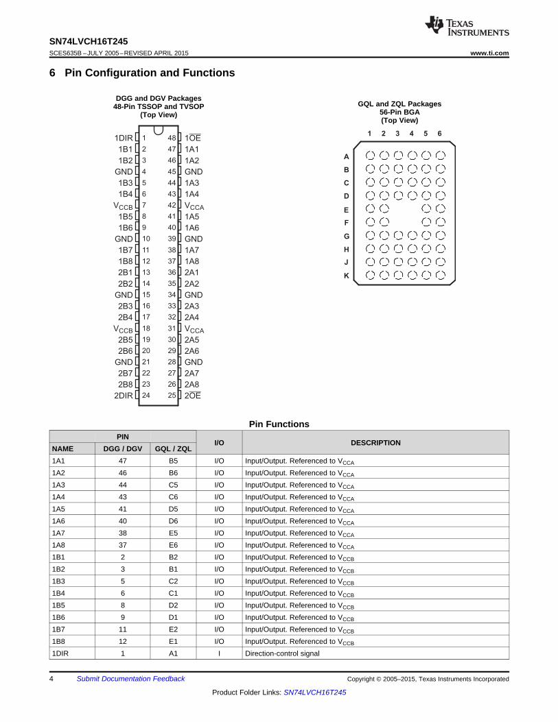
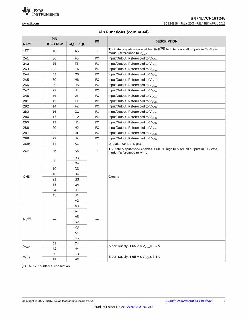
6 Pin Configuration and Functions
DGG and DGV PackagesGQL and ZQL Packages48-Pin TSSOP and TVSOP
56-Pin BGA(Top View)(Top View)
Pin FunctionsPIN
I/O DESCRIPTIONNAME DGG / DGV GQL / ZQL1A1 47 B5 I/O Input/Output. Referenced to VCCA
1A2 46 B6 I/O Input/Output. Referenced to VCCA
1A3 44 C5 I/O Input/Output. Referenced to VCCA
1A4 43 C6 I/O Input/Output. Referenced to VCCA
1A5 41 D5 I/O Input/Output. Referenced to VCCA
1A6 40 D6 I/O Input/Output. Referenced to VCCA
1A7 38 E5 I/O Input/Output. Referenced to VCCA
1A8 37 E6 I/O Input/Output. Referenced to VCCA
1B1 2 B2 I/O Input/Output. Referenced to VCCB
1B2 3 B1 I/O Input/Output. Referenced to VCCB
1B3 5 C2 I/O Input/Output. Referenced to VCCB
1B4 6 C1 I/O Input/Output. Referenced to VCCB
1B5 8 D2 I/O Input/Output. Referenced to VCCB
1B6 9 D1 I/O Input/Output. Referenced to VCCB
1B7 11 E2 I/O Input/Output. Referenced to VCCB
1B8 12 E1 I/O Input/Output. Referenced to VCCB
1DIR 1 A1 I Direction-control signal
4 Submit Documentation Feedback Copyright © 2005–2015, Texas Instruments Incorporated
Product Folder Links: SN74LVCH16T245
SN74LVCH16T245www.ti.com SCES635B –JULY 2005–REVISED APRIL 2015
Pin Functions (continued)PIN
I/O DESCRIPTIONNAME DGG / DGV GQL / ZQL
Tri-State output-mode enables. Pull OE high to place all outputs in Tri-State1OE 48 A6 I mode. Referenced to VCCA
2A1 36 F6 I/O Input/Output. Referenced to VCCA
2A2 35 F5 I/O Input/Output. Referenced to VCCA
2A3 33 G6 I/O Input/Output. Referenced to VCCA
2A4 32 G5 I/O Input/Output. Referenced to VCCA
2A5 30 H6 I/O Input/Output. Referenced to VCCA
2A6 29 H5 I/O Input/Output. Referenced to VCCA
2A7 27 J6 I/O Input/Output. Referenced to VCCA
2A8 26 J5 I/O Input/Output. Referenced to VCCA
2B1 13 F1 I/O Input/Output. Referenced to VCCB
2B2 14 F2 I/O Input/Output. Referenced to VCCB
2B3 16 G1 I/O Input/Output. Referenced to VCCB
2B4 17 G2 I/O Input/Output. Referenced to VCCB
2B5 19 H1 I/O Input/Output. Referenced to VCCB
2B6 20 H2 I/O Input/Output. Referenced to VCCB
2B7 22 J1 I/O Input/Output. Referenced to VCCB
2B8 23 J2 I/O Input/Output. Referenced to VCCB
2DIR 24 K1 I Direction-control signalTri-State output-mode enables. Pull OE high to place all outputs in Tri-State2OE 25 K6 I mode. Referenced to VCCA
B34
B410 D315 D4
GND — Ground21 G328 G434 J345 J4
A2A3A4A5
NC (1) — —K2K3K4K5
31 C4VCCA — A-port supply. 1.65 V ≤ VCCA≤ 5.5 V
42 H47 C3
VCCB — B-port supply. 1.65 V ≤ VCCB≤ 5.5 V18 H3
(1) NC – No internal connection
Copyright © 2005–2015, Texas Instruments Incorporated Submit Documentation Feedback 5
Product Folder Links: SN74LVCH16T245
SN74LVCH16T245SCES635B –JULY 2005–REVISED APRIL 2015 www.ti.com
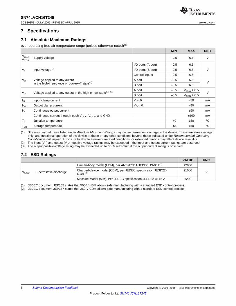
7 Specifications
7.1 Absolute Maximum Ratingsover operating free-air temperature range (unless otherwise noted) (1)
MIN MAX UNITVCCA Supply voltage –0.5 6.5 VVCCB
I/O ports (A port) –0.5 6.5VI Input voltage (2) I/O ports (B port) –0.5 6.5 V
Control inputs –0.5 6.5VO Voltage applied to any output A port –0.5 6.5
Vin the high-impedance or power-off state (2)B port –0.5 6.5A port –0.5 VCCA + 0.5
VO Voltage applied to any output in the high or low state (2) (3) VB port –0.5 VCCB + 0.5
IIK Input clamp current VI < 0 –50 mAIOK Output clamp current VO < 0 –50 mAIO Continuous output current ±50 mA
Continuous current through each VCCA, VCCB, and GND ±100 mATJ Junction temperature -40 150 °CTstg Storage temperature –65 150 °C
(1) Stresses beyond those listed under Absolute Maximum Ratings may cause permanent damage to the device. These are stress ratingsonly, and functional operation of the device at these or any other conditions beyond those indicated under Recommended OperatingConditions is not implied. Exposure to absolute-maximum-rated conditions for extended periods may affect device reliability.
(2) The input (VI ) and output (VO) negative-voltage ratings may be exceeded if the input and output current ratings are observed.(3) The output positive-voltage rating may be exceeded up to 6.5 V maximum if the output current rating is observed.
7.2 ESD RatingsVALUE UNIT
Human-body model (HBM), per ANSI/ESDA/JEDEC JS-001 (1) ±2000Charged-device model (CDM), per JEDEC specification JESD22- ±1000V(ESD) Electrostatic discharge VC101 (2)
Machine Model (MM), Per JEDEC specification JESD22-A115-A ±200
(1) JEDEC document JEP155 states that 500-V HBM allows safe manufacturing with a standard ESD control process.(2) JEDEC document JEP157 states that 250-V CDM allows safe manufacturing with a standard ESD control process.
6 Submit Documentation Feedback Copyright © 2005–2015, Texas Instruments Incorporated
Product Folder Links: SN74LVCH16T245
SN74LVCH16T245www.ti.com SCES635B –JULY 2005–REVISED APRIL 2015
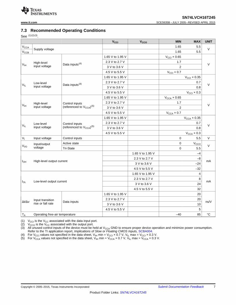
7.3 Recommended Operating ConditionsSee (1) (2) (3).
VCCI VCCO MIN MAX UNITVCCA 1.65 5.5
Supply voltage VVCCB 1.65 5.5
1.65 V to 1.95 V VCCI × 0.652.3 V to 2.7 V 1.7High-levelVIH Data inputs (4) Vinput voltage 3 V to 3.6 V 24.5 V to 5.5 V VCCI × 0.7
1.65 V to 1.95 V VCCI × 0.352.3 V to 2.7 V 0.7Low-levelVIL Data inputs (4) Vinput voltage 3 V to 3.6 V 0.84.5 V to 5.5 V VCCI × 0.3
1.65 V to 1.95 V VCCA × 0.652.3 V to 2.7 V 1.7High-level Control inputsVIH Vinput voltage (referenced to VCCA) (5) 3 V to 3.6 V 24.5 V to 5.5 V VCCA × 0.7
1.65 V to 1.95 V VCCA × 0.352.3 V to 2.7 V 0.7Low-level Control inputsVIL Vinput voltage (referenced to VCCA)(5) 3 V to 3.6 V 0.84.5 V to 5.5 V VCCA × 0.3
VI Input voltage Control inputs 0 5.5 VActive state 0 VCCOInput/outputVI/O Vvoltage Tri-State 0 5.5
1.65 V to 1.95 V –42.3 V to 2.7 V –8
IOH High-level output current mA3 V to 3.6 V –24
4.5 V to 5.5 V –321.65 V to 1.95 V 4
2.3 V to 2.7 V 8IOL Low-level output current mA
3 V to 3.6 V 244.5 V to 5.5 V 32
1.65 V to 1.95 V 202.3 V to 2.7 V 20Input transitionΔt/Δv Data inputs ns/Vrise or fall rate 3 V to 3.6 V 104.5 V to 5.5 V 5
TA Operating free-air temperature –40 85 °C
(1) VCCI is the VCC associated with the data input port.(2) VCCO is the VCC associated with the output port.(3) All unused control inputs of the device must be held at VCCA GND to ensure proper device operation and minimize power consumption.
Refer to the TI application report, Implications of Slow or Floating CMOS Inputs, SCBA004.(4) For VCCI values not specified in the data sheet, VIH min = VCCI × 0.7 V, VIL max = VCCI × 0.3 V.(5) For VCCA values not specified in the data sheet, VIH min = VCCA × 0.7 V, VIL max = VCCA × 0.3 V.
Copyright © 2005–2015, Texas Instruments Incorporated Submit Documentation Feedback 7
Product Folder Links: SN74LVCH16T245
SN74LVCH16T245SCES635B –JULY 2005–REVISED APRIL 2015 www.ti.com
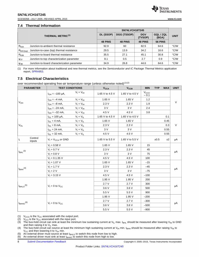
7.4 Thermal InformationSN74LVCH16T245
DL (SSOP) DGG (TSSOP) DGV GQL / ZQLTHERMAL METRIC (1) UNIT(TVSOP) (BGA)48 PINS 48 PINS 48 PINS 56 PINS
RθJA Junction-to-ambient thermal resistance 92.9 60 82.5 64.6 °C/WRθJC(top) Junction-to-case (top) thermal resistance 29.5 13.9 34.2 16.6 °C/WRθJB Junction-to-board thermal resistance 35.5 27.1 45.1 30.8 °C/WψJT Junction-to-top characterization parameter 8.1 0.5 2.7 0.9 °C/WψJB Junction-to-board characterization parameter 34.9 26.8 44.6 64.6 °C/W
(1) For more information about traditional and new thermal metrics, see the Semiconductor and IC Package Thermal Metrics applicationreport, SPRA953.
7.5 Electrical Characteristicsover recommended operating free-air temperature range (unless otherwise noted) (1) (2)
PARAMETER TEST CONDITIONS VCCA VCCB MIN TYP MAX UNITVI = VIH VCCOIOH = –100 μA, 1.65 V to 4.5 V 1.65 V to 4.5 V – 0.1
IOH = –4 mA, VI = VIH 1.65 V 1.65 V 1.2VOH VIOH = –8 mA, VI = VIH 2.3 V 2.3 V 1.9
IOH = –24 mA, VI = VIH 3 V 3 V 2.4IOH = –32 mA, VI = VIH 4.5 V 4.5 V 3.8IOL = 100 μA, VI = VIL 1.65 V to 4.5 V 1.65 V to 4.5 V 0.1IOL = 4 mA, VI = VIL 1.65 V 1.65 V 0.45
VOL IOL = 8 mA, VI = VIL 2.3 V 2.3 V 0.3 VIOL = 24 mA, VI = VIL 3 V 3 V 0.55IOL = 32 mA, VI = VIL 4.5 V 4.5 V 0.55
ControlII VI = VCCA or GND 1.65 V to 5.5 V 1.65 V to 5.5 V ±0.5 ±2 μAinputsVI = 0.58 V 1.65 V 1.65 V 15VI = 0.7 V 2.3 V 2.3 V 45
IBHL(3) μA
VI = 0.8 V 3 V 3 V 75VI = 0.1.35 V 4.5 V 4.5 V 100VI = 1.07 V 1.65 V 1.65 V –15VI = 1.7 V 2.3 V 2.3 V –45
IBHH(4) μA
VI = 2 V 3 V 3 V –75VI = 3.15 V 4.5 V 4.5 V –100
1.95 V 1.95 V 2002.7 V 2.7 V 300
IBHLO(5) VI = 0 to VCC μA
3.6 V 3.6 V 5005.5 V 5.5 V 9001.95 V 1.95 V –2002.7 V 2.7 V –300
IBHHO(6) VI = 0 to VCC μA
3.6 V 3.6 V –5005.5 V 5.5 V –900
(1) VCCO is the VCC associated with the output port.(2) VCCI is the VCC associated with the input port.(3) The bus-hold circuit can sink at least the minimum low sustaining current at VIL max. IBHL should be measured after lowering VIN to GND
and then raising it to VIL max.(4) The bus-hold circuit can source at least the minimum high sustaining current at VIH min. IBHH should be measured after raising VIN to
VCC and then lowering it to VIH min.(5) An external driver must source at least IBHLO to switch this node from low to high.(6) An external driver must sink at least IBHHO to switch this node from high to low.
8 Submit Documentation Feedback Copyright © 2005–2015, Texas Instruments Incorporated
Product Folder Links: SN74LVCH16T245
SN74LVCH16T245www.ti.com SCES635B –JULY 2005–REVISED APRIL 2015
Electrical Characteristics (continued)over recommended operating free-air temperature range (unless otherwise noted)(1)(2)
PARAMETER TEST CONDITIONS VCCA VCCB MIN TYP MAX UNITA port 0 V 0 to 5.5 V ±0.5 ±2
Ioff VI or VO = 0 to 5.5 V μAB port 0 to 5.5 V 0 V ±0.5 ±2A or B OE = VIH 1.65 V to 5.5 V 1.65 V to 5.5 V ±2port VO = VCCO or GND,IOZ μAB port VI = VCCI or GND 0 V 5.5 V ±2OE = don't
careA port 5.5 V 0 V ±21.65 V to 5.5 V 1.65 V to 5.5 V 20
ICCA VI = VCCI or GND, IO = 0 5 V 0 V 20 μA0 V 5 V –2
1.65 V to 5.5 V 1.65 V to 5.5 V 20ICCB VI = VCCI or GND, IO = 0 5 V 0 V –2 μA
0 V 5 V 20ICCA + 1.65 V to 5.5 V 1.65 V to 5.5 V 30VI = VCCI or GND, IO = 0 μAICCB
DIR at VCCA – 0.6 V,ΔICCA DIR B port = open, 3 V to 5.5 V 3 V to 5.5 V 50 μA
A port at VCCA or GNDControlCi VI = VCCA or GND 3.3 V 3.3 V 4 5 pFinputsA or BCio VO = VCCA/B or GND 3.3 V 3.3 V 8.5 10 pFport
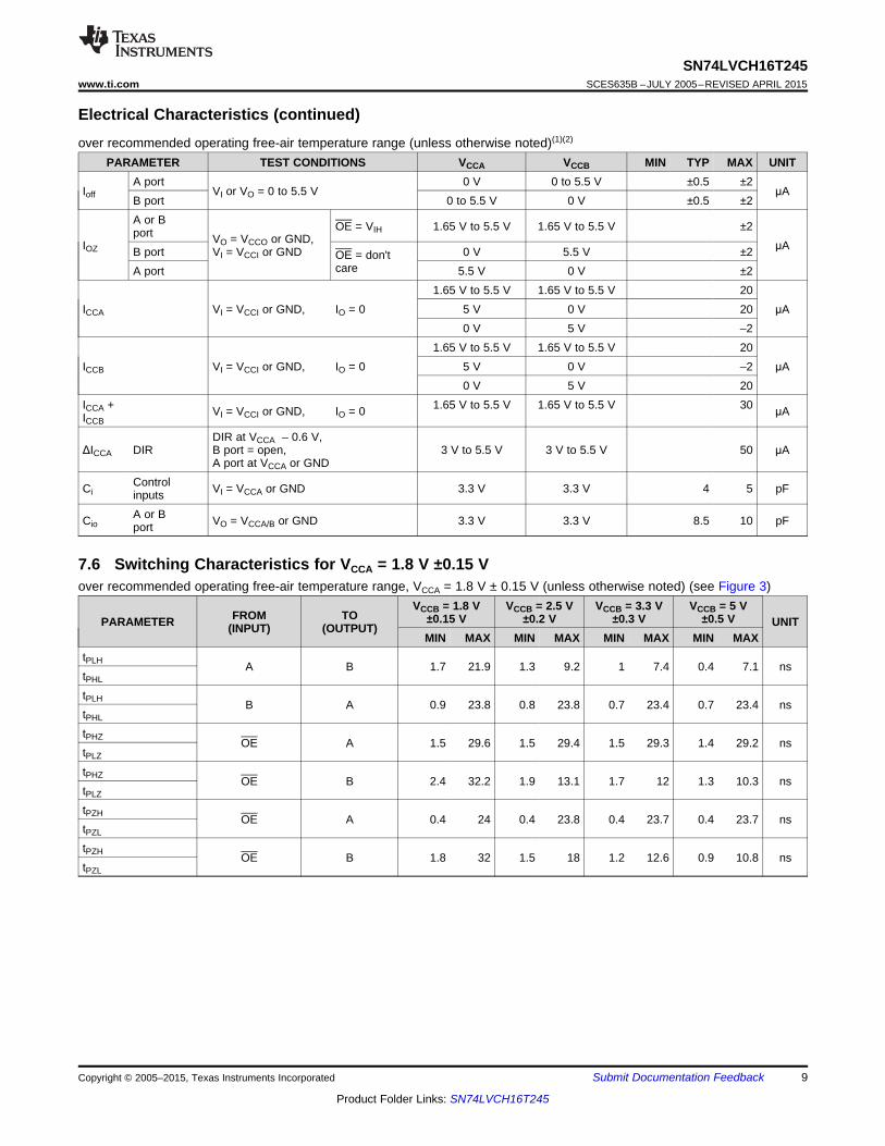
7.6 Switching Characteristics for VCCA = 1.8 V ±0.15 Vover recommended operating free-air temperature range, VCCA = 1.8 V ± 0.15 V (unless otherwise noted) (see Figure 3)
VCCB = 1.8 V VCCB = 2.5 V VCCB = 3.3 V VCCB = 5 VFROM TO ±0.15 V ±0.2 V ±0.3 V ±0.5 VPARAMETER UNIT(INPUT) (OUTPUT)
MIN MAX MIN MAX MIN MAX MIN MAXtPLH A B 1.7 21.9 1.3 9.2 1 7.4 0.4 7.1 nstPHL
tPLH B A 0.9 23.8 0.8 23.8 0.7 23.4 0.7 23.4 nstPHL
tPHZ OE A 1.5 29.6 1.5 29.4 1.5 29.3 1.4 29.2 nstPLZ
tPHZ OE B 2.4 32.2 1.9 13.1 1.7 12 1.3 10.3 nstPLZ
tPZH OE A 0.4 24 0.4 23.8 0.4 23.7 0.4 23.7 nstPZL
tPZH OE B 1.8 32 1.5 18 1.2 12.6 0.9 10.8 nstPZL
Copyright © 2005–2015, Texas Instruments Incorporated Submit Documentation Feedback 9
Product Folder Links: SN74LVCH16T245
SN74LVCH16T245SCES635B –JULY 2005–REVISED APRIL 2015 www.ti.com
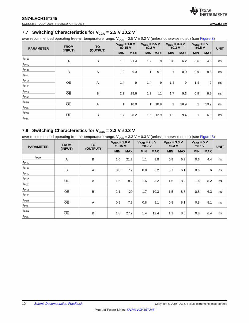
7.7 Switching Characteristics for VCCA = 2.5 V ±0.2 Vover recommended operating free-air temperature range, VCCA = 2.5 V ± 0.2 V (unless otherwise noted) (see Figure 3)
VCCB = 1.8 V VCCB = 2.5 V VCCB = 3.3 V VCCB = 5 VFROM TO ±0.15 V ±0.2 V ±0.3 V ±0.5 VPARAMETER UNIT(INPUT) (OUTPUT)
MIN MAX MIN MAX MIN MAX MIN MAXtPLH A B 1.5 21.4 1.2 9 0.8 6.2 0.6 4.8 nstPHL
tPLH B A 1.2 9.3 1 9.1 1 8.9 0.9 8.8 nstPHL
tPHZ OE A 1.4 9 1.4 9 1.4 9 1.4 9 nstPLZ
tPHZ OE B 2.3 29.6 1.8 11 1.7 9.3 0.9 6.9 nstPLZ
tPZH OE A 1 10.9 1 10.9 1 10.9 1 10.9 nstPZL
tPZH OE B 1.7 28.2 1.5 12.9 1.2 9.4 1 6.9 nstPZL
7.8 Switching Characteristics for VCCA = 3.3 V ±0.3 Vover recommended operating free-air temperature range, VCCA = 3.3 V ± 0.3 V (unless otherwise noted) (see Figure 3)
VCCB = 1.8 V VCCB = 2.5 V VCCB = 3.3 V VCCB = 5 VFROM TO ±0.15 V ±0.2 V ±0.3 V ±0.5 VPARAMETER UNIT(INPUT) (OUTPUT)
MIN MAX MIN MAX MIN MAX MIN MAXtPLH A B 1.6 21.2 1.1 8.8 0.8 6.2 0.6 4.4 ns
tPHL
tPLH B A 0.8 7.2 0.8 6.2 0.7 6.1 0.6 6 nstPHL
tPHZ OE A 1.6 8.2 1.6 8.2 1.6 8.2 1.6 8.2 nstPLZ
tPHZ OE B 2.1 29 1.7 10.3 1.5 8.8 0.8 6.3 nstPLZ
tPZH OE A 0.8 7.8 0.8 8.1 0.8 8.1 0.8 8.1 nstPZL
tPZH OE B 1.8 27.7 1.4 12.4 1.1 8.5 0.8 6.4 nstPZL
10 Submit Documentation Feedback Copyright © 2005–2015, Texas Instruments Incorporated
Product Folder Links: SN74LVCH16T245
SN74LVCH16T245www.ti.com SCES635B –JULY 2005–REVISED APRIL 2015
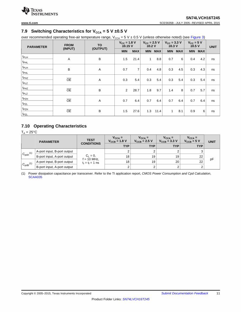
7.9 Switching Characteristics for VCCA = 5 V ±0.5 Vover recommended operating free-air temperature range, VCCA = 5 V ± 0.5 V (unless otherwise noted) (see Figure 3)
VCC = 1.8 V VCC = 2.5 V VCC = 3.3 V VCC = 5 VFROM TO ±0.15 V ±0.2 V ±0.3 V ±0.5 VPARAMETER UNIT(INPUT) (OUTPUT)
MIN MAX MIN MAX MIN MAX MIN MAXtPLH A B 1.5 21.4 1 8.8 0.7 6 0.4 4.2 nstPHL
tPLH B A 0.7 7 0.4 4.8 0.3 4.5 0.3 4.3 nstPHL
tPHZ OE A 0.3 5.4 0.3 5.4 0.3 5.4 0.3 5.4 nstPLZ
tPHZ OE B 2 28.7 1.8 9.7 1.4 8 0.7 5.7 nstPLZ
tPZH OE A 0.7 6.4 0.7 6.4 0.7 6.4 0.7 6.4 nstPZL
tPZH OE B 1.5 27.6 1.3 11.4 1 8.1 0.9 6 nstPZL
7.10 Operating CharacteristicsTA = 25°C
VCCA = VCCA = VCCA = VCCA =TEST VCCB = 1.8 V VCCB = 2.5 V VCCB = 3.3 V VCCB = 5 VPARAMETER UNITCONDITIONS
TYP TYP TYP TYPA-port input, B-port output 2 2 2 3
CpdA(1)
CL = 0,B-port input, A-port output 18 19 19 22f = 10 MHz, pF
A-port input, B-port output 18 19 20 22tr = tf = 1 nsCpdB(1)
B-port input, A-port output 2 2 2 2
(1) Power dissipation capacitance per transceiver. Refer to the TI application report, CMOS Power Consumption and Cpd Calculation,SCAA035
Copyright © 2005–2015, Texas Instruments Incorporated Submit Documentation Feedback 11
Product Folder Links: SN74LVCH16T245
0
0.2
0.4
0.6
0.8
1.0
1.2
1.4
0 20 40 60 80 100
VV
olta
ge
(V)
OL
I Current (mA)OL
-40 Co
25 Co
85 Co
4.4
4.6
4.8
5.0
5.2
5.4
5.6
0 -20 -40 -60 -80 -100
VV
olta
ge
(V)
OH
I Current (mA)OH
-40 Co
25 Co
85 Co
4.2
SN74LVCH16T245SCES635B –JULY 2005–REVISED APRIL 2015 www.ti.com
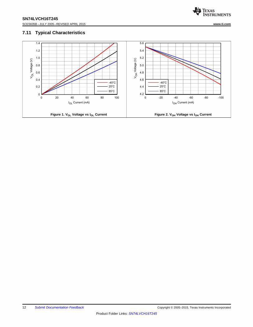
7.11 Typical Characteristics
Figure 1. VOL Voltage vs IOL Current Figure 2. VOH Voltage vs IOH Current
12 Submit Documentation Feedback Copyright © 2005–2015, Texas Instruments Incorporated
Product Folder Links: SN74LVCH16T245
VOH
VOL
From Output
Under Test
CL
(see Note A)
LOAD CIRCUIT
S1
2Ψ VCCO
Open
GND
RL
RL
tPLH tPHL
Output
Control
(low-level
enabling)
Output
Waveform 1
S1 at 2 ΨVCCO
(see Note B)
Output
Waveform 2
S1 at GND
(see Note B)
tPZL
tPZH
tPLZ
tPHZ
VCCA/2VCCA/2
VCCI/2 VCCI/2
VCCI
0 V
VCCO/2 VCCO/2
VOH
VOL
0 V
VCCO/2VOL + VTP
VCCO/2VOH − VTP
0 V
VCCI
0 V
VCCI/2 VCCI/2
tw
Input
VCCA
VCCO
VOLTAGE WAVEFORMS
PROPAGATION DELAY TIMES
VOLTAGE WAVEFORMS
PULSE DURATION
VOLTAGE WAVEFORMS
ENABLE AND DISABLE TIMES
Output
Input
tpd
tPLZ/tPZL
tPHZ/tPZH
Open
2 ΨVCCO
GND
TEST S1
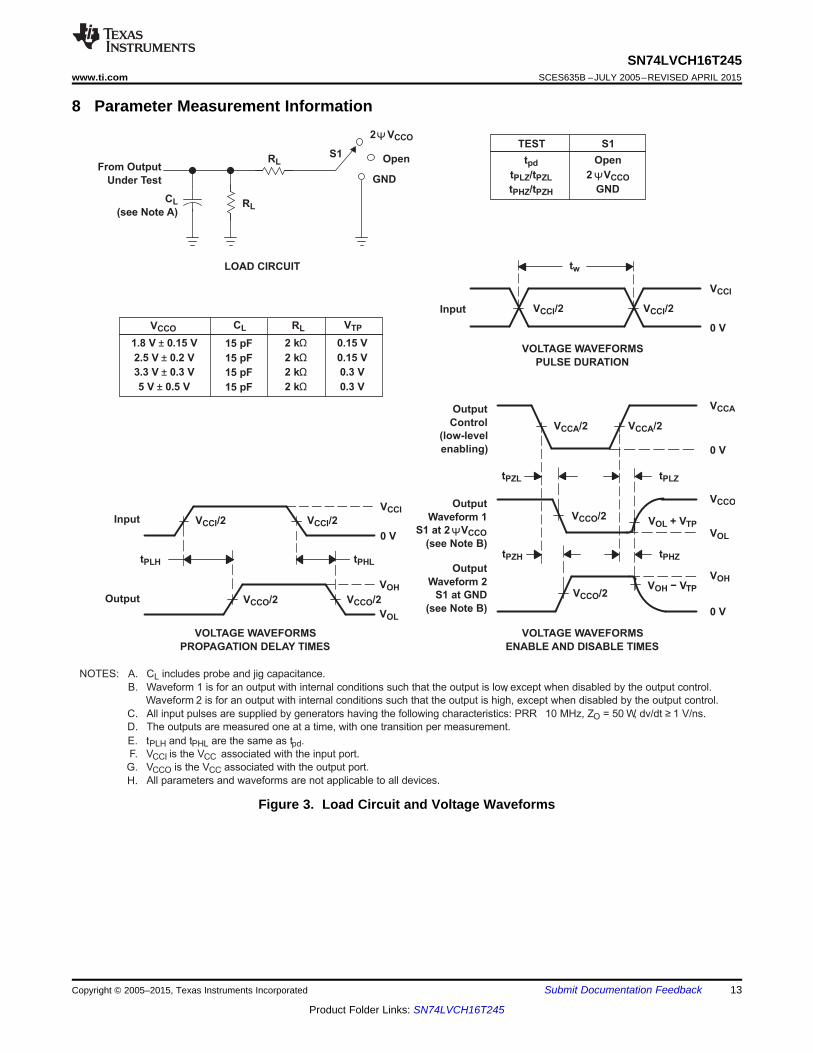
NOTES: A. CL includes probe and jig capacitance.
B. Waveform 1 is for an output with internal conditions such that the output is low, except when disabled by the output control.
Waveform 2 is for an output with internal conditions such that the output is high, except when disabled by the output control.
C. All input pulses are supplied by generators having the following characteristics: PRR 10 MHz, ZO = 50 W, dv/dt ≥ 1 V/ns.
D. The outputs are measured one at a time, with one transition per measurement.
E. tPLH and tPHL are the same as tpd.
F. VCCI is the VCC associated with the input port.
G. VCCO is the VCC associated with the output port.
H. All parameters and waveforms are not applicable to all devices.
1.8 V ± 0.15 V
2.5 V ± 0.2 V
3.3 V ± 0.3 V
5 V ± 0.5 V
2 kΩ
2 kΩ
2 kΩ
2 kΩ
VCCO RL
0.15 V
0.15 V
0.3 V
0.3 V
VTPCL
15 pF
15 pF
15 pF
15 pF
SN74LVCH16T245www.ti.com SCES635B –JULY 2005–REVISED APRIL 2015
8 Parameter Measurement Information
Figure 3. Load Circuit and Voltage Waveforms
Copyright © 2005–2015, Texas Instruments Incorporated Submit Documentation Feedback 13
Product Folder Links: SN74LVCH16T245
To Seven Other Channels
1DIR
1A1
1B1
1OE
To Seven Other Channels
2DIR
2A1
2B1
2OE
1
47
24
36
48
2
25
13
SN74LVCH16T245SCES635B –JULY 2005–REVISED APRIL 2015 www.ti.com
9 Detailed Description
9.1 OverviewThe SN74LVCH16T245 is a 16-bit, dual-supply noninverting bidirectional voltage level translation. Pins AX andcontrol pins (DIR and OE) are supported by VCCA and pins BX are supported by VCCB. The A port is able toaccept I/O voltages ranging from 1.65 V to 5.5 V, while the B port can accept I/O voltages from 1.65 V to 5.5 V.A high on DIR allows data transmission from A to B and a low on DIR allows data transmission from B to A whenOE is set to low. When OE is set to high, both A and B are in the high-impedance state.
This device has Active bus-hold circuitry that holds unused or undriven inputs at a valid logic state. This device isfully specified for partial-power-down applications using off output current (Ioff).
The VCC isolation feature ensures that if either VCC input is at GND, both ports are put in a high-impedance state.
9.2 Functional Block Diagram
9.3 Feature Description
9.3.1 Fully Configurable Dual-Rail Design Allows Each Port to Operate Over the Full 1.65-V to 5.5-VPower-Supply Range
Both VCCA and VCCB can be supplied at any voltage from 1.65 V to 5.5 V making the device suitable fortranslating between any of the low voltage nodes (1.8-V, 2.5-V, and 3.3-V).
9.3.2 Support High-Speed TranslationSN74LVCH16T245 can support high data rate application. Data rates can be calculated form the maximumpropagation delay. This is also dependant on the output load. For example, for a 3.3-V to 5-V conversion, themaximum frequency is 200 MHz.
9.3.3 Partial-Power-Down Mode OperationThis device is fully specified for partial-power-down applications using off output current (Ioff). Ioff will preventbackflow current by disabling I/O output circuits when device is in partial power-down mode.
9.3.4 VCC IsolationThe VCC isolation feature ensures that if either VCCA or VCCB are at GND, both ports will be in a high-impedancestate (IOZ shown in Electrical Characteristics). This prevents false logic levels from being presented to either bus.
9.3.5 Bus Hold on Data InputsActive bus-hold circuitry holds unused or undriven inputs at a valid logic state. Use of pullup or pulldown resistorswith the bus-hold circuitry is not recommended.
14 Submit Documentation Feedback Copyright © 2005–2015, Texas Instruments Incorporated
Product Folder Links: SN74LVCH16T245
SN74LVCH16T245www.ti.com SCES635B –JULY 2005–REVISED APRIL 2015
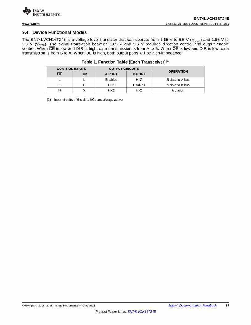
9.4 Device Functional ModesThe SN74LVCH16T245 is a voltage level translator that can operate from 1.65 V to 5.5 V (VCCA) and 1.65 V to5.5 V (VCCB). The signal translation between 1.65 V and 5.5 V requires direction control and output enablecontrol. When OE is low and DIR is high, data transmission is from A to B. When OE is low and DIR is low, datatransmission is from B to A. When OE is high, both output ports will be high-impedance.
Table 1. Function Table (Each Transceiver) (1)
CONTROL INPUTS OUTPUT CIRCUITSOPERATION
OE DIR A PORT B PORTL L Enabled Hi-Z B data to A busL H Hi-Z Enabled A data to B busH X Hi-Z Hi-Z Isolation
(1) Input circuits of the data I/Os are always active.
Copyright © 2005–2015, Texas Instruments Incorporated Submit Documentation Feedback 15
Product Folder Links: SN74LVCH16T245
SN74LVCH16T245SCES635B –JULY 2005–REVISED APRIL 2015 www.ti.com
10 Application and Implementation
NOTEInformation in the following applications sections is not part of the TI componentspecification, and TI does not warrant its accuracy or completeness. TI’s customers areresponsible for determining suitability of components for their purposes. Customers shouldvalidate and test their design implementation to confirm system functionality.
10.1 Application InformationThe SN74LVCH16T245 device can be used in level-shifting applications for interfacing devices and addressingmixed voltage incompatibility. The SN74LVCH16T245 device is ideal for data transmission where direction isdifferent for each channel.
10.1.1 Enable TimesCalculate the enable times for the SN74LVCH16T245 using the following formulas:
tPZH (DIR to A) = tPLZ (DIR to B) + tPLH (B to A) (1)tPZL (DIR to A) = tPHZ (DIR to B) + tPHL (B to A) (2)tPZH (DIR to B) = tPLZ (DIR to A) + tPLH (A to B) (3)tPZL (DIR to B) = tPHZ (DIR to A) + tPHL (A to B) (4)
In a bidirectional application, these enable times provide the maximum delay from the time the DIR bit isswitched until an output is expected. For example, if the SN74LVCH16T245 initially is transmitting from A to B,then the DIR bit is switched; the B port of the device must be disabled before presenting it with an input. After theB port has been disabled, an input signal applied to it appears on the corresponding A port after the specifiedpropagation delay.
16 Submit Documentation Feedback Copyright © 2005–2015, Texas Instruments Incorporated
Product Folder Links: SN74LVCH16T245
SN74LVCH16T245
1OE/2OE
1DIR/2DIR
1A1/2A1
1A2/2A2
1A3/2A3
1A4/2A4
1.8-V
Controller
VCCA VCCB
1B1/2B1
1B2/2B2
1B3/2B3
1B4/2B4
3.3-V
System
1.8 V
0.1 µF 0.1 µF 1 µF
3.3 V
GND GND GND
Data Data1A5/2A5
1A6/2A6
1A7/2A7
1A8/2A8
1B5/2B5
1B6/2B6
1B7/2B7
1B8/2B8
SN74LVCH16T245www.ti.com SCES635B –JULY 2005–REVISED APRIL 2015
10.2 Typical Application
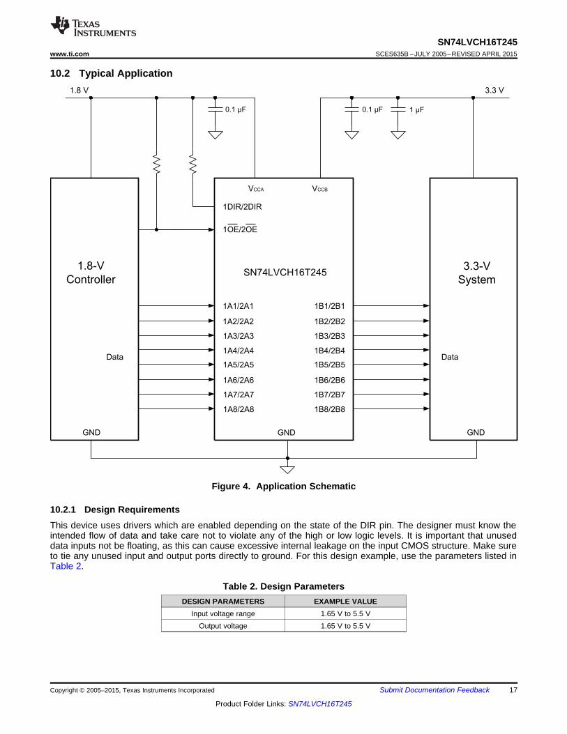
Figure 4. Application Schematic
10.2.1 Design RequirementsThis device uses drivers which are enabled depending on the state of the DIR pin. The designer must know theintended flow of data and take care not to violate any of the high or low logic levels. It is important that unuseddata inputs not be floating, as this can cause excessive internal leakage on the input CMOS structure. Make sureto tie any unused input and output ports directly to ground. For this design example, use the parameters listed inTable 2.
Table 2. Design ParametersDESIGN PARAMETERS EXAMPLE VALUE
Input voltage range 1.65 V to 5.5 VOutput voltage 1.65 V to 5.5 V
Copyright © 2005–2015, Texas Instruments Incorporated Submit Documentation Feedback 17
Product Folder Links: SN74LVCH16T245
Time (200 ns/div)
Output (5 V)
Input (1.8 V)
Voltage (
V)
SN74LVCH16T245SCES635B –JULY 2005–REVISED APRIL 2015 www.ti.com
10.2.2 Detailed Design ProcedureTo begin the design process, determine the following:• Input voltage range
– Use the supply voltage of the device that is driving the SN74LVCH16T245 device to determine the inputvoltage range. For a valid logic high the value must exceed the VIH of the input port. For a valid logic lowthe value must be less than the VIL of the input port.
• Output voltage range– Use the supply voltage of the device that the SN74LVCH16T245 device is driving to determine the output
voltage range.
10.2.3 Application Curve
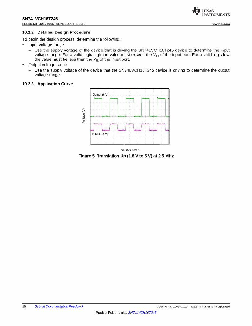
Figure 5. Translation Up (1.8 V to 5 V) at 2.5 MHz
18 Submit Documentation Feedback Copyright © 2005–2015, Texas Instruments Incorporated
Product Folder Links: SN74LVCH16T245
SN74LVCH16T245www.ti.com SCES635B –JULY 2005–REVISED APRIL 2015
11 Power Supply RecommendationsThe SN74LVCH16T245 device uses two separate configurable power-supply rails, VCCA and VCCB. VCCA acceptsany supply voltage from 1.65 V to 5.5 V and VCCB accepts any supply voltage from 1.65 V to 5.5 V. The A portand B port are designed to track VCCA and VCCB, respectively, allowing for low-voltage bidirectional translationbetween any of the 1.8-V, 2.5-V and 3.3-V voltage nodes.
The output-enable OE input circuit is designed so that it is supplied by VCCA and when the OE input is high, alloutputs are placed in the high-impedance state. To ensure the high-impedance state of the outputs during powerup or power down, the OE input pin must be tied to VCCA through a pullup resistor and must not be enabled untilVCCA and VCCB are fully ramped and stable. The minimum value of the pullup resistor to VCCA is determined bythe current-sinking capability of the driver.
12 Layout
12.1 Layout GuidelinesTo ensure reliability of the device, following common printed-circuit-board layout guidelines is recommended.• Bypass capacitors should be used on power supplies.• Short trace lengths should be used to avoid excessive loading.• Placing pads on the signal paths for loading capacitors or pullup resistors to help adjust rise and fall times of
signals depending on the system requirements.
Copyright © 2005–2015, Texas Instruments Incorporated Submit Documentation Feedback 19
Product Folder Links: SN74LVCH16T245
22
19
20
21
23
24
2B5
2B6
GND
2B7
2B8
2DIR
GND
1A2
1OE
LEGEND
VIA to Power Plane
VIA to GND Plane (Inner Layer)
Polygonal Copper Pour
44
1A8
VCCA
1A3
1A4
37
ToSystem
SN74AVCH16T245
VC
CA
Keep OE high until VCCA and VCCB are powered up
1A1
41
GND
1A5
1A6
39
1A7 38
35
34
33
32
31
29
28
2A5
2A2
2A1
2A4
GND
2A3
VCCA
2A6
GND
2A7
2A8
31
2OE
1
GND
1B2
1DIR
2
3
4
5
1B8
VCCB
1B3
1B46
7
12
1B1
8 1B5
1B69
10
1B711
13
14
15
16
17
2B2
2B1
2B4
GND
2B3
VCCB18
From Controller
Bypass Capacitor
VC
CA
ToSystem
ToSystem
ToSystem
ToSystem
ToSystem
ToSystem
ToSystem
From Controller
From Controller
From Controller
From Controller
From Controller
From Controller
From Controller
From Controller
From Controller
From Controller
From Controller
From Controller
From Controller
From Controller
From Controller
GND
ToSystem
ToSystem
ToSystem
ToSystem
VC
CA
VC
CA
Keep OE high until VCCA and VCCB are powered up
27
48
47
46
45
42
ToSystem
ToSystem
ToSystem
ToSystem
43
40
36
26
25
VCCB VCCA
VCCB
Bypass Capacitor
VCCA
SN74LVCH16T245SCES635B –JULY 2005–REVISED APRIL 2015 www.ti.com
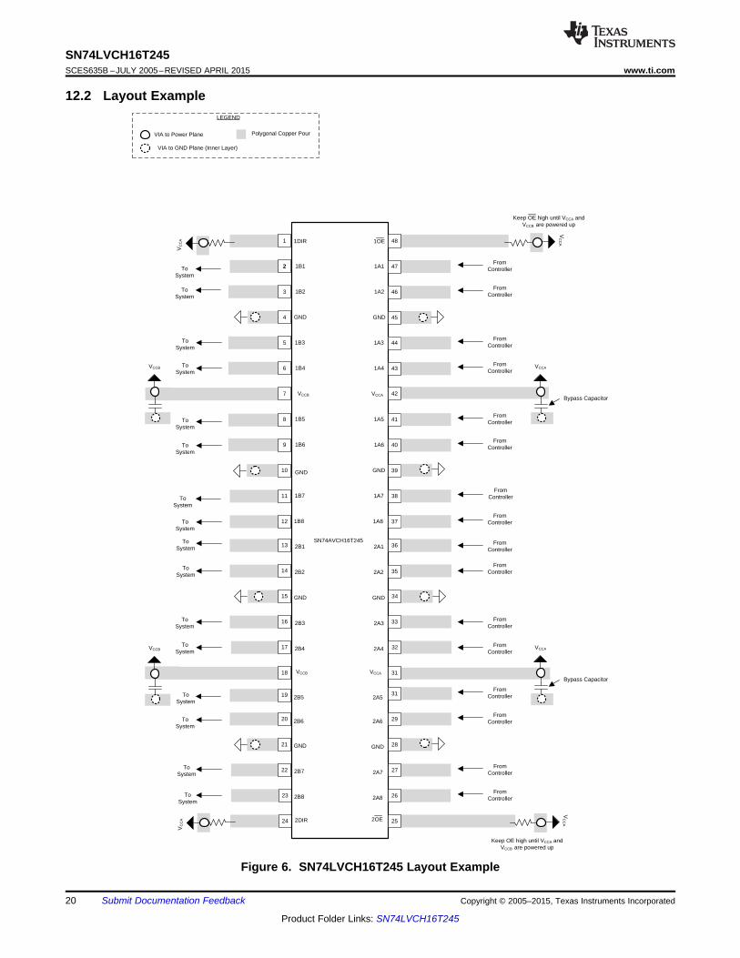
12.2 Layout Example
Figure 6. SN74LVCH16T245 Layout Example
20 Submit Documentation Feedback Copyright © 2005–2015, Texas Instruments Incorporated
Product Folder Links: SN74LVCH16T245
SN74LVCH16T245www.ti.com SCES635B –JULY 2005–REVISED APRIL 2015
13 Device and Documentation Support
13.1 Documentation Support
13.1.1 Related DocumentationFor related documentation see the following:• CMOS Power Consumption and Cpd Calculation, SCAA035• Implications of Slow or Floating CMOS Inputs, SCBA004
13.2 TrademarksAll trademarks are the property of their respective owners.
13.3 Electrostatic Discharge CautionThese devices have limited built-in ESD protection. The leads should be shorted together or the device placed in conductive foamduring storage or handling to prevent electrostatic damage to the MOS gates.
13.4 GlossarySLYZ022 — TI Glossary.
This glossary lists and explains terms, acronyms, and definitions.
14 Mechanical, Packaging, and Orderable InformationThe following pages include mechanical, packaging, and orderable information. This information is the mostcurrent data available for the designated devices. This data is subject to change without notice and revision ofthis document. For browser-based versions of this data sheet, refer to the left-hand navigation.
Copyright © 2005–2015, Texas Instruments Incorporated Submit Documentation Feedback 21
Product Folder Links: SN74LVCH16T245
PACKAGE OPTION ADDENDUM
www.ti.com 24-Aug-2018
Addendum-Page 1
PACKAGING INFORMATION
Orderable Device Status(1)
Package Type PackageDrawing
Pins PackageQty
Eco Plan(2)
Lead/Ball Finish(6)
MSL Peak Temp(3)
Op Temp (°C) Device Marking(4/5)
Samples
74LVCH16T245DGGRE4 ACTIVE TSSOP DGG 48 2000 Green (RoHS& no Sb/Br)
CU NIPDAU Level-1-260C-UNLIM -40 to 85 LVCH16T245
74LVCH16T245DLG4 ACTIVE SSOP DL 48 25 Green (RoHS& no Sb/Br)
CU NIPDAU Level-1-260C-UNLIM -40 to 85 LVCH16T245
74LVCH16T245ZQLR ACTIVE BGAMICROSTAR
JUNIOR
ZQL 56 1000 Green (RoHS& no Sb/Br)
SNAGCU Level-1-260C-UNLIM -40 to 85 NL245
SN74LVCH16T245DGGR ACTIVE TSSOP DGG 48 2000 Green (RoHS& no Sb/Br)
CU NIPDAU Level-1-260C-UNLIM -40 to 85 LVCH16T245
SN74LVCH16T245DGVR ACTIVE TVSOP DGV 48 2000 Green (RoHS& no Sb/Br)
CU NIPDAU Level-1-260C-UNLIM -40 to 85 LDHT245
SN74LVCH16T245DL ACTIVE SSOP DL 48 25 Green (RoHS& no Sb/Br)
CU NIPDAU Level-1-260C-UNLIM -40 to 85 LVCH16T245
SN74LVCH16T245DLR ACTIVE SSOP DL 48 1000 Green (RoHS& no Sb/Br)
CU NIPDAU Level-1-260C-UNLIM -40 to 85 LVCH16T245
SN74LVCH16T245KR NRND BGAMICROSTAR
JUNIOR
GQL 56 1000 TBD SNPB Level-1-240C-UNLIM -40 to 85 LDHT245
(1) The marketing status values are defined as follows:ACTIVE: Product device recommended for new designs.LIFEBUY: TI has announced that the device will be discontinued, and a lifetime-buy period is in effect.NRND: Not recommended for new designs. Device is in production to support existing customers, but TI does not recommend using this part in a new design.PREVIEW: Device has been announced but is not in production. Samples may or may not be available.OBSOLETE: TI has discontinued the production of the device.
(2) RoHS: TI defines "RoHS" to mean semiconductor products that are compliant with the current EU RoHS requirements for all 10 RoHS substances, including the requirement that RoHS substancedo not exceed 0.1% by weight in homogeneous materials. Where designed to be soldered at high temperatures, "RoHS" products are suitable for use in specified lead-free processes. TI mayreference these types of products as "Pb-Free".RoHS Exempt: TI defines "RoHS Exempt" to mean products that contain lead but are compliant with EU RoHS pursuant to a specific EU RoHS exemption.Green: TI defines "Green" to mean the content of Chlorine (Cl) and Bromine (Br) based flame retardants meet JS709B low halogen requirements of <=1000ppm threshold. Antimony trioxide basedflame retardants must also meet the <=1000ppm threshold requirement.
(3) MSL, Peak Temp. - The Moisture Sensitivity Level rating according to the JEDEC industry standard classifications, and peak solder temperature.
(4) There may be additional marking, which relates to the logo, the lot trace code information, or the environmental category on the device.
PACKAGE OPTION ADDENDUM
www.ti.com 24-Aug-2018
Addendum-Page 2
(5) Multiple Device Markings will be inside parentheses. Only one Device Marking contained in parentheses and separated by a "~" will appear on a device. If a line is indented then it is a continuationof the previous line and the two combined represent the entire Device Marking for that device.
(6) Lead/Ball Finish - Orderable Devices may have multiple material finish options. Finish options are separated by a vertical ruled line. Lead/Ball Finish values may wrap to two lines if the finishvalue exceeds the maximum column width.
Important Information and Disclaimer:The information provided on this page represents TI's knowledge and belief as of the date that it is provided. TI bases its knowledge and belief on informationprovided by third parties, and makes no representation or warranty as to the accuracy of such information. Efforts are underway to better integrate information from third parties. TI has taken andcontinues to take reasonable steps to provide representative and accurate information but may not have conducted destructive testing or chemical analysis on incoming materials and chemicals.TI and TI suppliers consider certain information to be proprietary, and thus CAS numbers and other limited information may not be available for release.
In no event shall TI's liability arising out of such information exceed the total purchase price of the TI part(s) at issue in this document sold by TI to Customer on an annual basis.
OTHER QUALIFIED VERSIONS OF SN74LVCH16T245 :
• Enhanced Product: SN74LVCH16T245-EP
NOTE: Qualified Version Definitions:
• Enhanced Product - Supports Defense, Aerospace and Medical Applications
TAPE AND REEL INFORMATION
*All dimensions are nominal
Device PackageType
PackageDrawing
Pins SPQ ReelDiameter
(mm)
ReelWidth
W1 (mm)
A0(mm)
B0(mm)
K0(mm)
P1(mm)
W(mm)
Pin1Quadrant
74LVCH16T245ZQLR BGA MI CROSTA
R JUNI OR
ZQL 56 1000 330.0 16.4 4.8 7.3 1.5 8.0 16.0 Q1
SN74LVCH16T245DGGR TSSOP DGG 48 2000 330.0 24.4 8.6 13.0 1.8 12.0 24.0 Q1
SN74LVCH16T245DGVR TVSOP DGV 48 2000 330.0 16.4 7.1 10.2 1.6 12.0 16.0 Q1
SN74LVCH16T245DLR SSOP DL 48 1000 330.0 32.4 11.35 16.2 3.1 16.0 32.0 Q1
SN74LVCH16T245KR BGA MI CROSTA
R JUNI OR
GQL 56 1000 330.0 16.4 4.8 7.3 1.5 8.0 16.0 Q1
PACKAGE MATERIALS INFORMATION
www.ti.com 11-Mar-2017
Pack Materials-Page 1
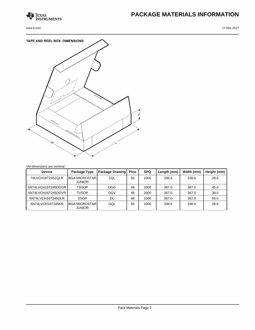
*All dimensions are nominal
Device Package Type Package Drawing Pins SPQ Length (mm) Width (mm) Height (mm)
74LVCH16T245ZQLR BGA MICROSTARJUNIOR
ZQL 56 1000 336.6 336.6 28.6
SN74LVCH16T245DGGR TSSOP DGG 48 2000 367.0 367.0 45.0
SN74LVCH16T245DGVR TVSOP DGV 48 2000 367.0 367.0 38.0
SN74LVCH16T245DLR SSOP DL 48 1000 367.0 367.0 55.0
SN74LVCH16T245KR BGA MICROSTARJUNIOR
GQL 56 1000 336.6 336.6 28.6
PACKAGE MATERIALS INFORMATION
www.ti.com 11-Mar-2017
Pack Materials-Page 2
MECHANICAL DATA
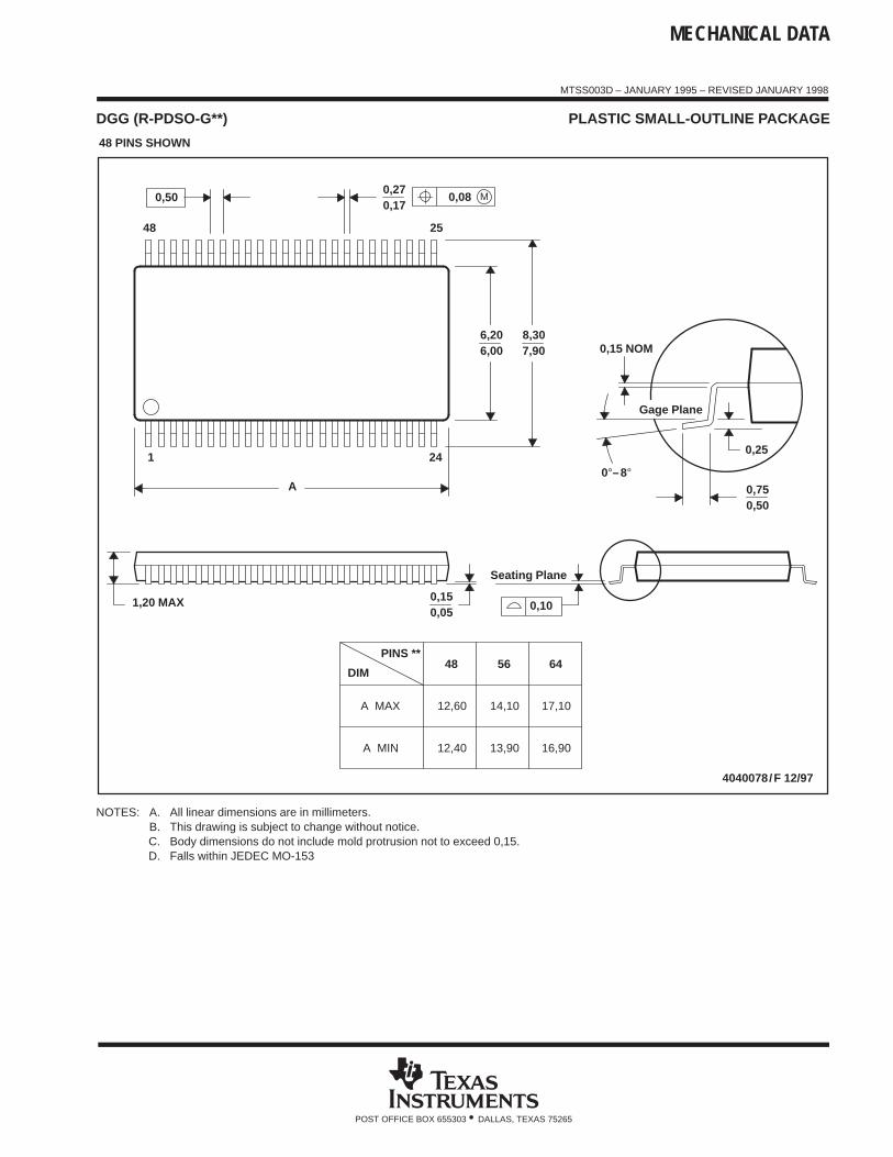
MTSS003D – JANUARY 1995 – REVISED JANUARY 1998
POST OFFICE BOX 655303 • DALLAS, TEXAS 75265
DGG (R-PDSO-G**) PLASTIC SMALL-OUTLINE PACKAGE
4040078/F 12/97
48 PINS SHOWN
0,25
0,15 NOM
Gage Plane
6,006,20 8,30
7,90
0,750,50
Seating Plane
25
0,270,17
24
A
48
1
1,20 MAX
M0,08
0,10
0,50
0°–8°
56
14,10
13,90
48DIM
A MAX
A MIN
PINS **
12,40
12,60
64
17,10
16,90
0,150,05
NOTES: A. All linear dimensions are in millimeters.B. This drawing is subject to change without notice.C. Body dimensions do not include mold protrusion not to exceed 0,15.D. Falls within JEDEC MO-153
www.ti.com
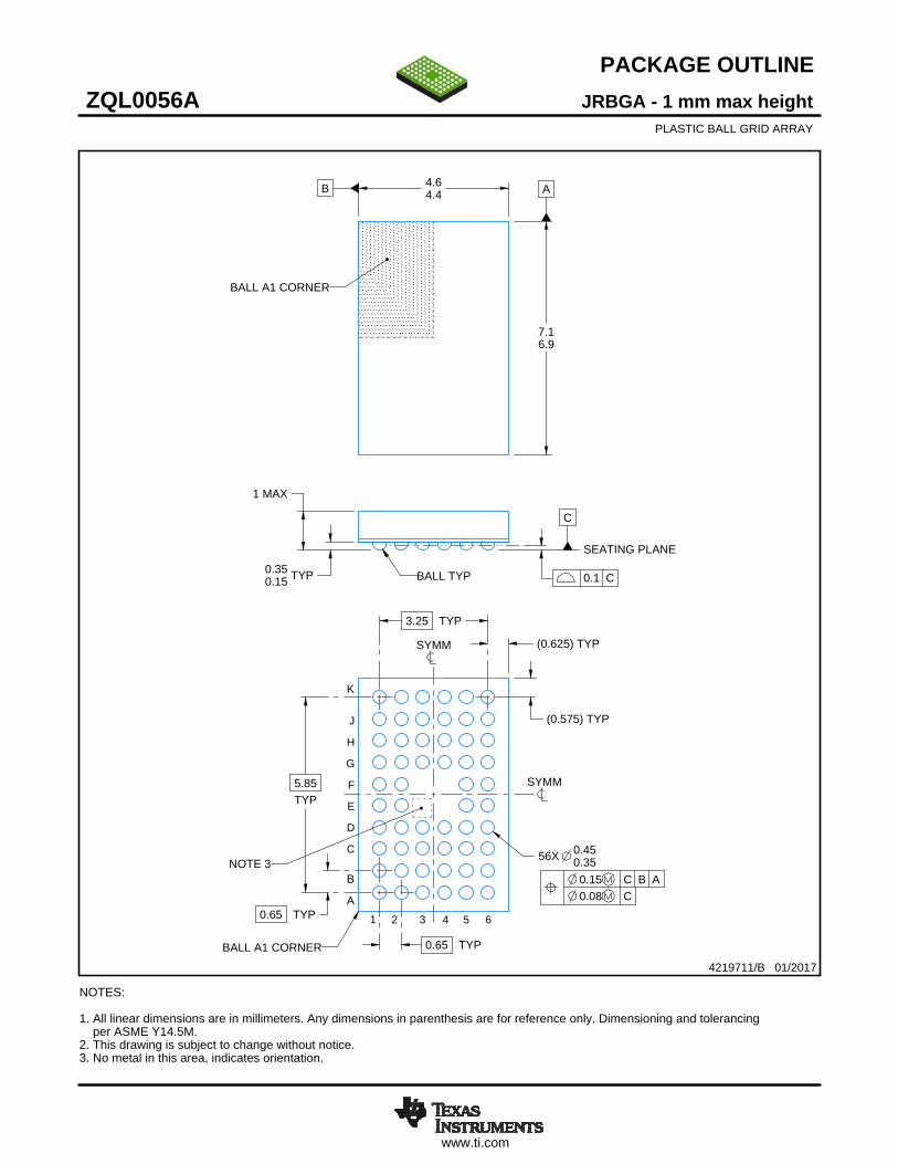
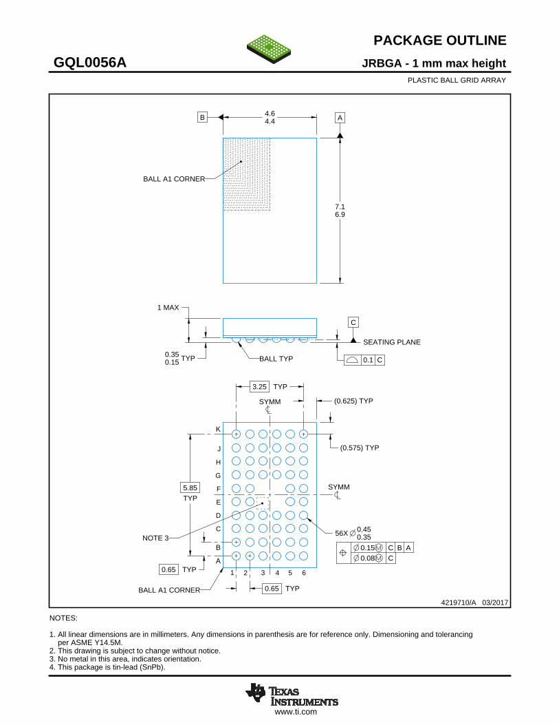
PACKAGE OUTLINE
C
1 MAX
TYP0.350.15
5.85TYP
3.25 TYP
0.65 TYP
0.65 TYP
56X 0.450.35
B 4.64.4 A
7.16.9
(0.625) TYP
(0.575) TYP
JRBGA - 1 mm max heightZQL0056APLASTIC BALL GRID ARRAY
4219711/B 01/2017
NOTES: 1. All linear dimensions are in millimeters. Any dimensions in parenthesis are for reference only. Dimensioning and tolerancing per ASME Y14.5M. 2. This drawing is subject to change without notice. 3. No metal in this area, indicates orientation.
BALL A1 CORNER
SEATING PLANE
BALL TYP 0.1 C
0.15 C B A0.08 C
SYMM
SYMM
BALL A1 CORNER
K
C
D
E
F
G
H
J
1 2 3 4 5 6
A
BNOTE 3
SCALE 2.100

www.ti.com
EXAMPLE BOARD LAYOUT
56X ( 0.33)(0.65) TYP
(0.65) TYP
( 0.33)METAL
0.05 MAXSOLDER MASKOPENING
METAL UNDERSOLDER MASK
( 0.33)SOLDER MASKOPENING
0.05 MIN
JRBGA - 1 mm max heightZQL0056APLASTIC BALL GRID ARRAY
4219711/B 01/2017
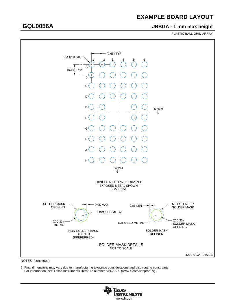
NOTES: (continued) 4. Final dimensions may vary due to manufacturing tolerance considerations and also routing constraints. For information, see Texas Instruments literature number SPRAA99 (www.ti.com/lit/spraa99).
SYMM
SYMM
LAND PATTERN EXAMPLEEXPOSED METAL SHOWN
SCALE:15X
1 2 3 4 5 6
A
C
D
E
F
G
H
J
K
B
NON-SOLDER MASKDEFINED
(PREFERRED)
SOLDER MASK DETAILSNOT TO SCALE
EXPOSED METAL
SOLDER MASKDEFINED
EXPOSED METAL

www.ti.com
EXAMPLE STENCIL DESIGN
(0.65) TYP
(0.65) TYP56X ( 0.33)
JRBGA - 1 mm max heightZQL0056APLASTIC BALL GRID ARRAY
4219711/B 01/2017
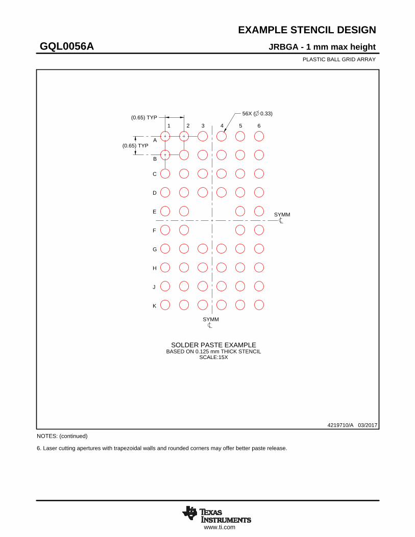
NOTES: (continued) 5. Laser cutting apertures with trapezoidal walls and rounded corners may offer better paste release.
SOLDER PASTE EXAMPLEBASED ON 0.125 mm THICK STENCIL
SCALE:15X
SYMM
SYMM
1 2 3 4 5 6
A
C
D
E
F
G
H
J
K
B
www.ti.com
PACKAGE OUTLINE
C
1 MAX
TYP0.350.15
5.85TYP
3.25 TYP
0.65 TYP
0.65 TYP
56X 0.450.35
B 4.64.4 A
7.16.9
(0.625) TYP
(0.575) TYP
JRBGA - 1 mm max heightGQL0056APLASTIC BALL GRID ARRAY
4219710/A 03/2017
NOTES: 1. All linear dimensions are in millimeters. Any dimensions in parenthesis are for reference only. Dimensioning and tolerancing per ASME Y14.5M. 2. This drawing is subject to change without notice. 3. No metal in this area, indicates orientation.4. This package is tin-lead (SnPb).
BALL A1 CORNER
SEATING PLANE
BALL TYP 0.1 C
0.15 C B A0.08 C
SYMM
SYMM
BALL A1 CORNER
K
C
D
E
F
G
H
J
1 2 3 4 5 6
A
BNOTE 3
SCALE 2.100
www.ti.com
EXAMPLE BOARD LAYOUT
56X ( 0.33)(0.65) TYP
(0.65) TYP
( 0.33)METAL
0.05 MAXSOLDER MASKOPENING
METAL UNDERSOLDER MASK
( 0.33)SOLDER MASKOPENING
0.05 MIN
JRBGA - 1 mm max heightGQL0056APLASTIC BALL GRID ARRAY
4219710/A 03/2017
NOTES: (continued) 5. Final dimensions may vary due to manufacturing tolerance considerations and also routing constraints. For information, see Texas Instruments literature number SPRAA99 (www.ti.com/lit/spraa99).
SYMM
SYMM
LAND PATTERN EXAMPLEEXPOSED METAL SHOWN
SCALE:15X
1 2 3 4 5 6
A
C
D
E
F
G
H
J
K
B
NON-SOLDER MASKDEFINED
(PREFERRED)
SOLDER MASK DETAILSNOT TO SCALE
EXPOSED METAL
SOLDER MASKDEFINED
EXPOSED METAL
www.ti.com
EXAMPLE STENCIL DESIGN
(0.65) TYP
(0.65) TYP56X ( 0.33)
JRBGA - 1 mm max heightGQL0056APLASTIC BALL GRID ARRAY
4219710/A 03/2017
NOTES: (continued) 6. Laser cutting apertures with trapezoidal walls and rounded corners may offer better paste release.
SOLDER PASTE EXAMPLEBASED ON 0.125 mm THICK STENCIL
SCALE:15X
SYMM
SYMM
1 2 3 4 5 6
A
C
D
E
F
G
H
J
K
B
IMPORTANT NOTICE
Texas Instruments Incorporated (TI) reserves the right to make corrections, enhancements, improvements and other changes to itssemiconductor products and services per JESD46, latest issue, and to discontinue any product or service per JESD48, latest issue. Buyersshould obtain the latest relevant information before placing orders and should verify that such information is current and complete.TI’s published terms of sale for semiconductor products (http://www.ti.com/sc/docs/stdterms.htm) apply to the sale of packaged integratedcircuit products that TI has qualified and released to market. Additional terms may apply to the use or sale of other types of TI products andservices.Reproduction of significant portions of TI information in TI data sheets is permissible only if reproduction is without alteration and isaccompanied by all associated warranties, conditions, limitations, and notices. TI is not responsible or liable for such reproduceddocumentation. Information of third parties may be subject to additional restrictions. Resale of TI products or services with statementsdifferent from or beyond the parameters stated by TI for that product or service voids all express and any implied warranties for theassociated TI product or service and is an unfair and deceptive business practice. TI is not responsible or liable for any such statements.Buyers and others who are developing systems that incorporate TI products (collectively, “Designers”) understand and agree that Designersremain responsible for using their independent analysis, evaluation and judgment in designing their applications and that Designers havefull and exclusive responsibility to assure the safety of Designers' applications and compliance of their applications (and of all TI productsused in or for Designers’ applications) with all applicable regulations, laws and other applicable requirements. Designer represents that, withrespect to their applications, Designer has all the necessary expertise to create and implement safeguards that (1) anticipate dangerousconsequences of failures, (2) monitor failures and their consequences, and (3) lessen the likelihood of failures that might cause harm andtake appropriate actions. Designer agrees that prior to using or distributing any applications that include TI products, Designer willthoroughly test such applications and the functionality of such TI products as used in such applications.TI’s provision of technical, application or other design advice, quality characterization, reliability data or other services or information,including, but not limited to, reference designs and materials relating to evaluation modules, (collectively, “TI Resources”) are intended toassist designers who are developing applications that incorporate TI products; by downloading, accessing or using TI Resources in anyway, Designer (individually or, if Designer is acting on behalf of a company, Designer’s company) agrees to use any particular TI Resourcesolely for this purpose and subject to the terms of this Notice.TI’s provision of TI Resources does not expand or otherwise alter TI’s applicable published warranties or warranty disclaimers for TIproducts, and no additional obligations or liabilities arise from TI providing such TI Resources. TI reserves the right to make corrections,enhancements, improvements and other changes to its TI Resources. TI has not conducted any testing other than that specificallydescribed in the published documentation for a particular TI Resource.Designer is authorized to use, copy and modify any individual TI Resource only in connection with the development of applications thatinclude the TI product(s) identified in such TI Resource. NO OTHER LICENSE, EXPRESS OR IMPLIED, BY ESTOPPEL OR OTHERWISETO ANY OTHER TI INTELLECTUAL PROPERTY RIGHT, AND NO LICENSE TO ANY TECHNOLOGY OR INTELLECTUAL PROPERTYRIGHT OF TI OR ANY THIRD PARTY IS GRANTED HEREIN, including but not limited to any patent right, copyright, mask work right, orother intellectual property right relating to any combination, machine, or process in which TI products or services are used. Informationregarding or referencing third-party products or services does not constitute a license to use such products or services, or a warranty orendorsement thereof. Use of TI Resources may require a license from a third party under the patents or other intellectual property of thethird party, or a license from TI under the patents or other intellectual property of TI.TI RESOURCES ARE PROVIDED “AS IS” AND WITH ALL FAULTS. TI DISCLAIMS ALL OTHER WARRANTIES ORREPRESENTATIONS, EXPRESS OR IMPLIED, REGARDING RESOURCES OR USE THEREOF, INCLUDING BUT NOT LIMITED TOACCURACY OR COMPLETENESS, TITLE, ANY EPIDEMIC FAILURE WARRANTY AND ANY IMPLIED WARRANTIES OFMERCHANTABILITY, FITNESS FOR A PARTICULAR PURPOSE, AND NON-INFRINGEMENT OF ANY THIRD PARTY INTELLECTUALPROPERTY RIGHTS. TI SHALL NOT BE LIABLE FOR AND SHALL NOT DEFEND OR INDEMNIFY DESIGNER AGAINST ANY CLAIM,INCLUDING BUT NOT LIMITED TO ANY INFRINGEMENT CLAIM THAT RELATES TO OR IS BASED ON ANY COMBINATION OFPRODUCTS EVEN IF DESCRIBED IN TI RESOURCES OR OTHERWISE. IN NO EVENT SHALL TI BE LIABLE FOR ANY ACTUAL,DIRECT, SPECIAL, COLLATERAL, INDIRECT, PUNITIVE, INCIDENTAL, CONSEQUENTIAL OR EXEMPLARY DAMAGES INCONNECTION WITH OR ARISING OUT OF TI RESOURCES OR USE THEREOF, AND REGARDLESS OF WHETHER TI HAS BEENADVISED OF THE POSSIBILITY OF SUCH DAMAGES.Unless TI has explicitly designated an individual product as meeting the requirements of a particular industry standard (e.g., ISO/TS 16949and ISO 26262), TI is not responsible for any failure to meet such industry standard requirements.Where TI specifically promotes products as facilitating functional safety or as compliant with industry functional safety standards, suchproducts are intended to help enable customers to design and create their own applications that meet applicable functional safety standardsand requirements. Using products in an application does not by itself establish any safety features in the application. Designers mustensure compliance with safety-related requirements and standards applicable to their applications. Designer may not use any TI products inlife-critical medical equipment unless authorized officers of the parties have executed a special contract specifically governing such use.Life-critical medical equipment is medical equipment where failure of such equipment would cause serious bodily injury or death (e.g., lifesupport, pacemakers, defibrillators, heart pumps, neurostimulators, and implantables). Such equipment includes, without limitation, allmedical devices identified by the U.S. Food and Drug Administration as Class III devices and equivalent classifications outside the U.S.TI may expressly designate certain products as completing a particular qualification (e.g., Q100, Military Grade, or Enhanced Product).Designers agree that it has the necessary expertise to select the product with the appropriate qualification designation for their applicationsand that proper product selection is at Designers’ own risk. Designers are solely responsible for compliance with all legal and regulatoryrequirements in connection with such selection.Designer will fully indemnify TI and its representatives against any damages, costs, losses, and/or liabilities arising out of Designer’s non-compliance with the terms and provisions of this Notice.
Mailing Address: Texas Instruments, Post Office Box 655303, Dallas, Texas 75265Copyright © 2018, Texas Instruments Incorporated


