A. Melloni, Progress in photonics, Firenze 2015
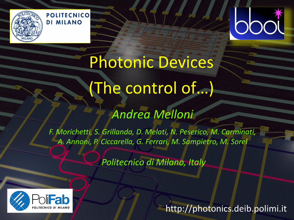
Photonic Devices
(The control of…)
Andrea Melloni
F. Morichetti, S. Grillanda, D. Melati, N. Peserico, M. Carminati, A. Annoni, P. Ciccarella, G. Ferrari, M. Sampietro, M. Sorel
Politecnico di Milano, Italy
http://photonics.deib.polimi.it
A. Melloni, Progress in photonics, Firenze 2015
400 m2
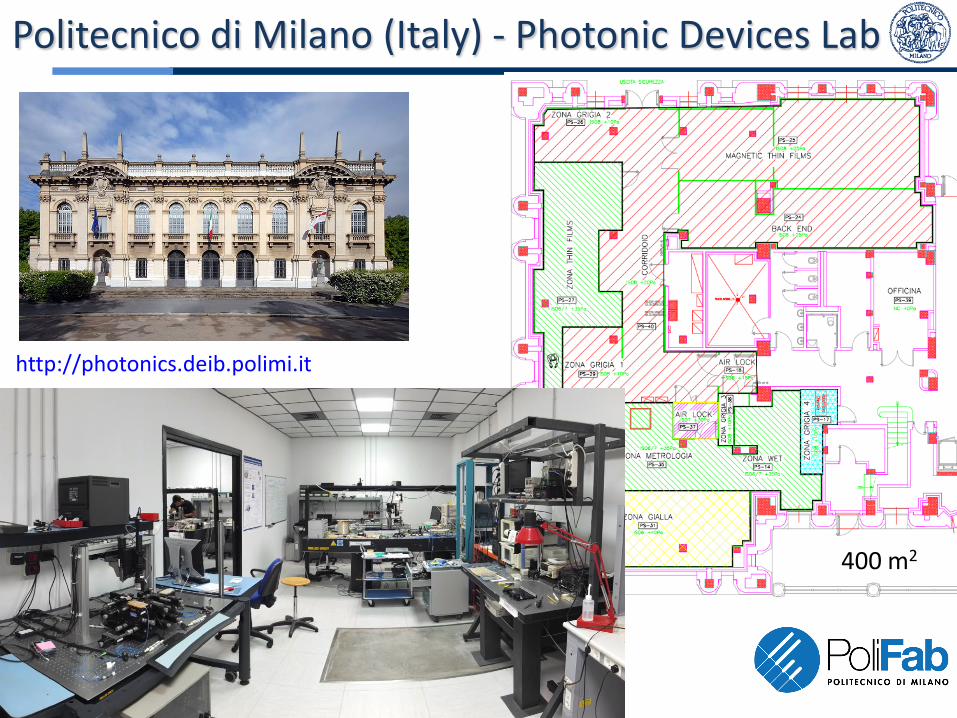
Politecnico di Milano (Italy) - Photonic Devices Lab
http://photonics.deib.polimi.it
A. Melloni, Progress in photonics, Firenze 2015
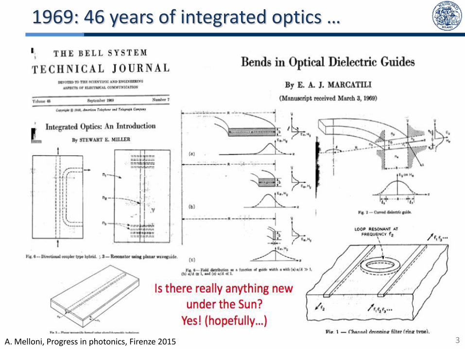
1969: 46 years of integrated optics …
3

A. Melloni, Progress in photonics, Firenze 2015
Integrated photonics: ubiquitousness and complexity
4
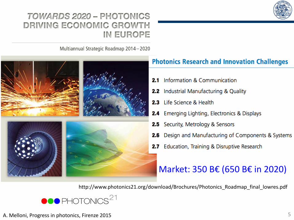
A. Melloni, Progress in photonics, Firenze 2015 5
http://www.photonics21.org/download/Brochures/Photonics_Roadmap_final_lowres.pdf
Market: 350 B€ (650 B€ in 2020)

A. Melloni, Progress in photonics, Firenze 2015
Technologies and Waveguides
Dn Ge:SiO2
0.5…3 %
SiON
2…8 %
Si3N4
38 %
SOI
140%
As2S3
60…100 %
InP
3 / 70 %
Mach-Zehnder D. Couplers, Y, MMI, Star couplers
Ring Resonators
Gratings
6
A. Melloni, Progress in photonics, Firenze 2015
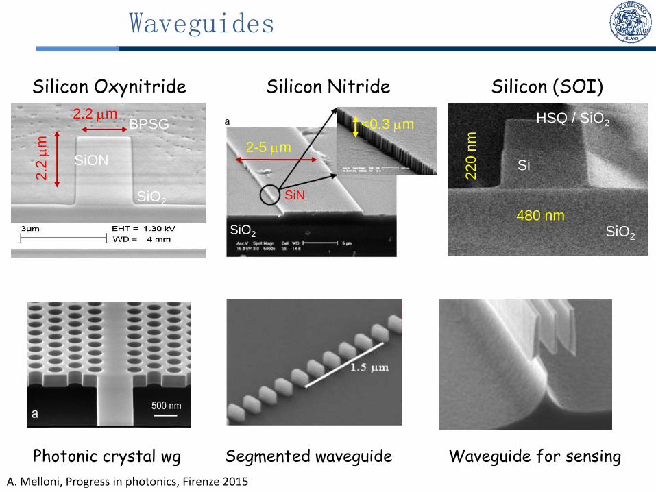
BPSG
SiO2
SiON
2.2
mm
2.2 mm
480 nm
220 n
m
HSQ / SiO2
SiO2
Si
Waveguides
Silicon Oxynitride Silicon Nitride Silicon (SOI)
<0.3 mm
2-5 mm
SiO2
SiN
Photonic crystal wg Segmented waveguide Waveguide for sensing
A. Melloni, Progress in photonics, Firenze 2015 8
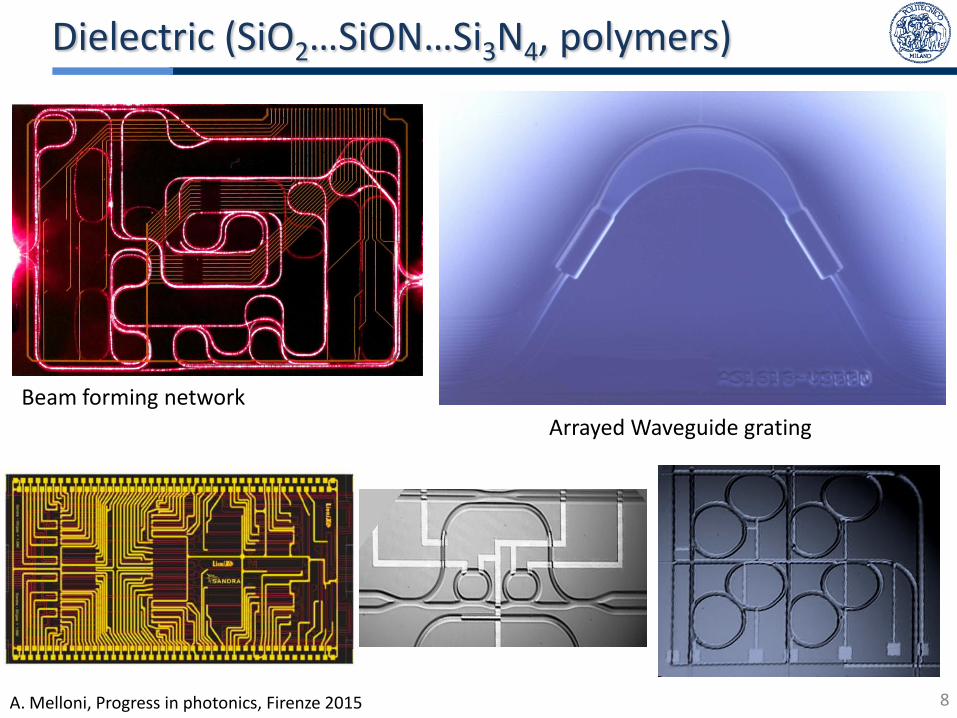
Dielectric (SiO2…SiON…Si3N4, polymers)
Beam forming network
Arrayed Waveguide grating
A. Melloni, Progress in photonics, Firenze 2015
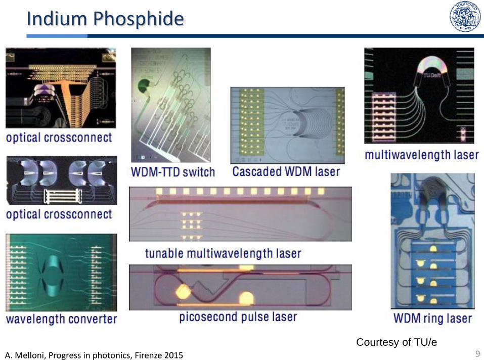
Courtesy of TU/e
Indium Phosphide
9
A. Melloni, Progress in photonics, Firenze 2015
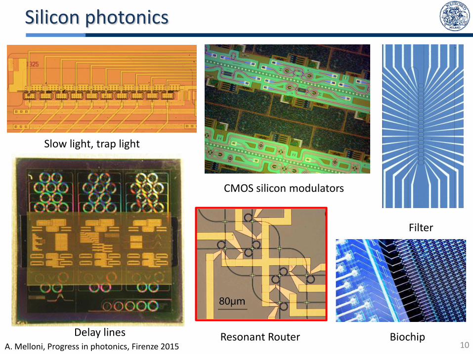
Silicon photonics
Slow light, trap light
Delay lines
CMOS silicon modulators
Resonant Router
Filter
Biochip 10
A. Melloni, Progress in photonics, Firenze 2015
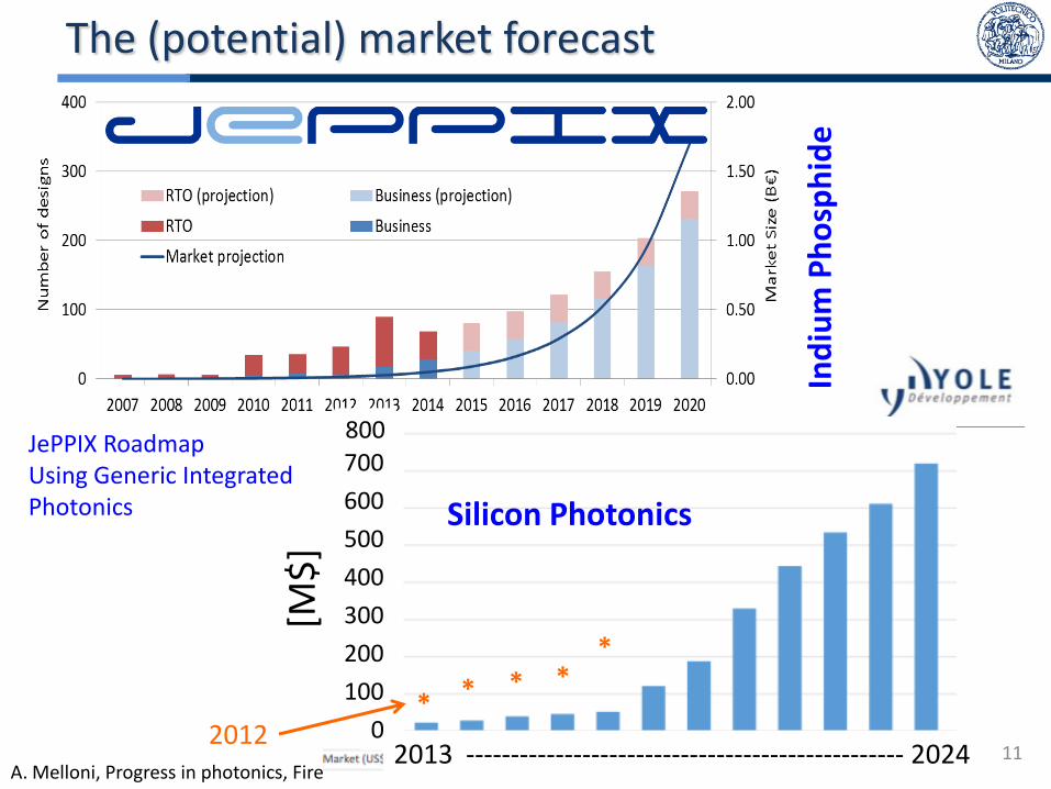
The (potential) market forecast
Ind
ium
Ph
osp
hid
e
JePPIX Roadmap Using Generic Integrated Photonics
* * *
* *
Silicon Photonics
100
200
300
400
500
600
700
[M$
]
2012 2013 ------------------------------------------------- 2024
0
800
11
A. Melloni, Progress in photonics, Firenze 2015
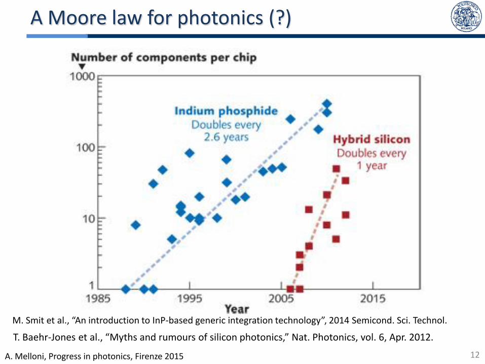
A Moore law for photonics (?)
T. Baehr-Jones et al., “Myths and rumours of silicon photonics,” Nat. Photonics, vol. 6, Apr. 2012.
12
M. Smit et al., “An introduction to InP-based generic integration technology”, 2014 Semicond. Sci. Technol.
A. Melloni, Progress in photonics, Firenze 2015
• Moore law in photonics… No scaling in photonics !
• Photonics as electronics…. Photonics is analog !
• Plasmonic, graphene, carbon nanotubes …
• CMOS compatibility… Mendeleev on chip !
• More Moore or More than Moore? … Integration, synergy
• Everyone does their job! … generic foundry scheme
• Control & feedback, toward “system-on-a-chip” paradigm
It’s a long way (in my view) …
13
A. Melloni, Progress in photonics, Firenze 2015
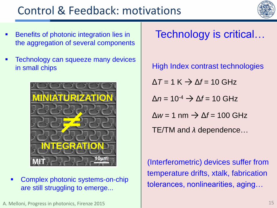
Control & Feedback: motivations
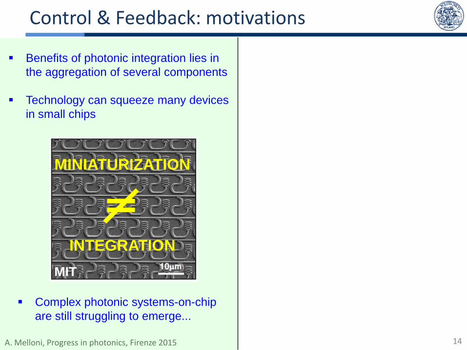
Benefits of photonic integration lies in
the aggregation of several components
Technology can squeeze many devices
in small chips
Complex photonic systems-on-chip
are still struggling to emerge...
MINIATURIZATION
INTEGRATION
MIT
14
A. Melloni, Progress in photonics, Firenze 2015
Control & Feedback: motivations
Benefits of photonic integration lies in
the aggregation of several components
Technology can squeeze many devices
in small chips
Complex photonic systems-on-chip
are still struggling to emerge...
MINIATURIZATION
INTEGRATION
MIT
Technology is critical…
(Interferometric) devices suffer from
temperature drifts, xtalk, fabrication
tolerances, nonlinearities, aging…
High Index contrast technologies
ΔT = 1 K → Δf = 10 GHz
Δn = 10-4 → Δf = 10 GHz
Δw = 1 nm → Δf = 100 GHz
TE/TM and λ dependence…
15
A. Melloni, Progress in photonics, Firenze 2015
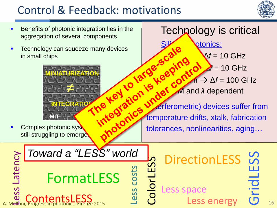
Technology is critical
(Interferometric) devices suffer from
temperature drifts, xtalk, fabrication
tolerances, nonlinearities, aging…
Benefits of photonic integration lies in the
aggregation of several components
Technology can squeeze many devices
in small chips
Complex photonic systems-on-chip are
still struggling to emerge...
MINIATURIZATION
INTEGRATION
MIT
Silicon Photonics:
ΔT = 1 K → Δf = 10 GHz
Δn = 10-4 → Δf = 10 GHz
Δw = 1 nm → Δf = 100 GHz
TE/TM and λ dependent ≠
Gri
dLE
SS
FormatLESS
ContentsLESS
DirectionLESS C
olo
rLES
S
Less energy Less space
Less
co
sts
Less
Lat
ency
Toward a “LESS” world
Control & Feedback: motivations
16
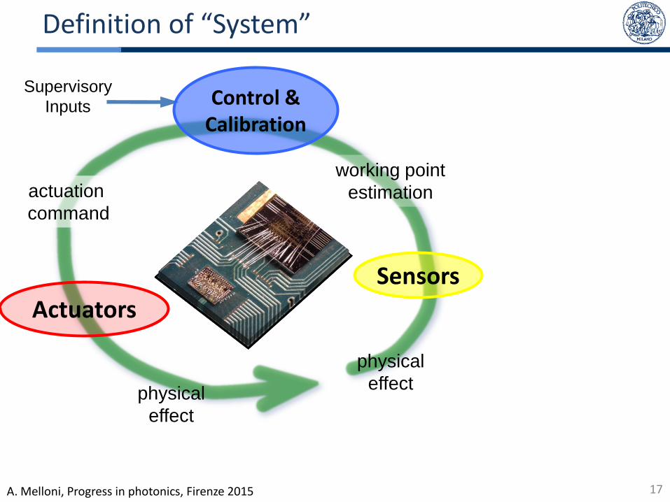
A. Melloni, Progress in photonics, Firenze 2015
physical
effect physical
effect
actuation
command
working point
estimation
Sensors
Actuators
Definition of “System”
Supervisory
Inputs Control & Calibration
17
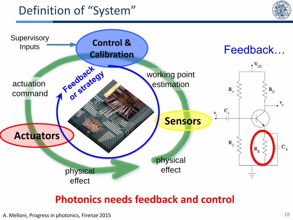
A. Melloni, Progress in photonics, Firenze 2015
physical
effect physical
effect
actuation
command
working point
estimation
Actuators
Photonics needs feedback and control
Definition of “System”
Supervisory
Inputs Control & Calibration Feedback…
Sensors
18
A. Melloni, Progress in photonics, Firenze 2015
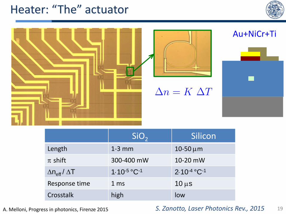
Au+NiCr+Ti
Heater: “The” actuator
SiO2 Silicon
Length 1-3 mm 10-50 mm
p shift 300-400 mW 10-20 mW
Dneff / DT 110-5 °C-1 210-4 °C-1
Response time 1 ms 10 ms
Crosstalk high low
19 S. Zanotto, Laser Photonics Rev., 2015
A. Melloni, Progress in photonics, Firenze 2015
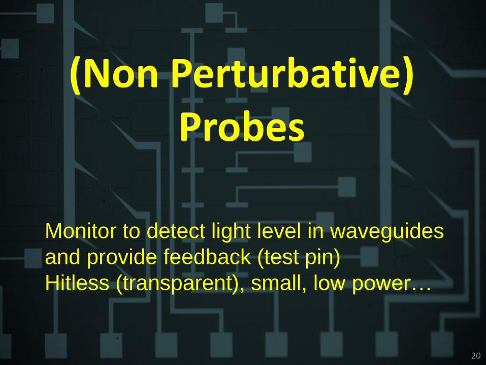
(Non Perturbative) Probes
Monitor to detect light level in waveguides
and provide feedback (test pin)
Hitless (transparent), small, low power…
20
A. Melloni, Progress in photonics, Firenze 2015
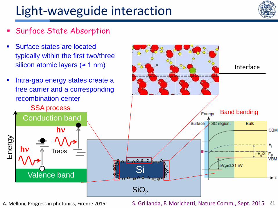
Light-waveguide interaction
Band bending
Si
SiO2
Valence band
Traps
Energ
y
hn
hn
Conduction band
SSA process
Interface
Surface State Absorption
Surface states are located
typically within the first two/three
silicon atomic layers (≈ 1 nm)
Intra-gap energy states create a
free carrier and a corresponding
recombination center
21 S. Grillanda, F. Morichetti, Nature Comm., Sept. 2015
A. Melloni, Progress in photonics, Firenze 2015
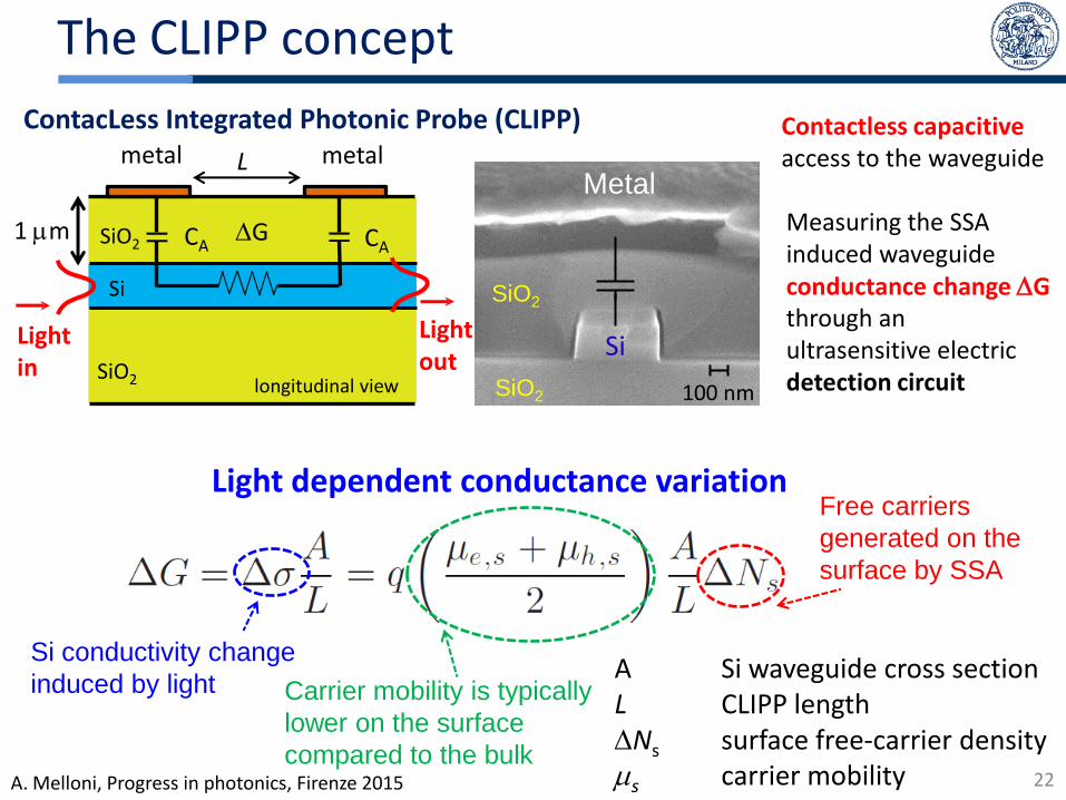
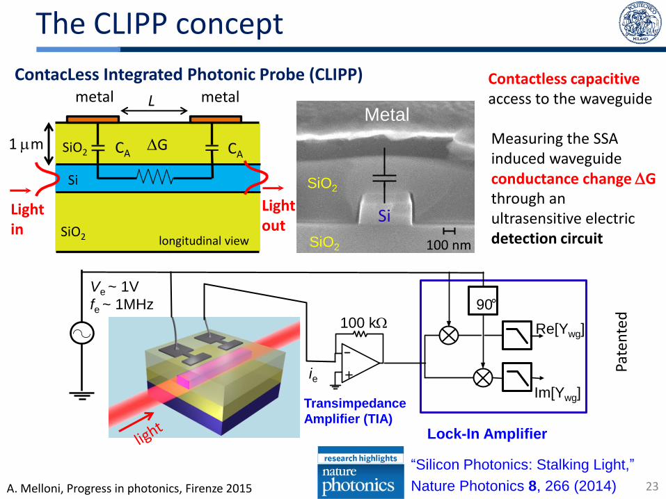
Measuring the SSA induced waveguide conductance change DG through an ultrasensitive electric detection circuit
Si
SiO2
DG CA CA SiO2
metal metal L
ContacLess Integrated Photonic Probe (CLIPP)
SiO2
SiO2
Metal
Si
100 nm
The CLIPP concept
1 mm
longitudinal view
Contactless capacitive access to the waveguide
Light in
Light out
A Si waveguide cross section L CLIPP length DNs surface free-carrier density ms carrier mobility
Light dependent conductance variation Free carriers
generated on the
surface by SSA
Carrier mobility is typically
lower on the surface
compared to the bulk
Si conductivity change
induced by light
22
A. Melloni, Progress in photonics, Firenze 2015
Measuring the SSA induced waveguide conductance change DG through an ultrasensitive electric detection circuit
Si
SiO2
DG CA CA SiO2
metal metal L
ContacLess Integrated Photonic Probe (CLIPP)
SiO2
SiO2
Metal
Si
100 nm
The CLIPP concept
1 mm
longitudinal view
Contactless capacitive access to the waveguide
Light in
Light out
Ve ~ 1V
fe ~ 1MHz
ie
90 °
Re[Ywg]
Lock-In Amplifier
100 kW V, f0
Im[Ywg]
+
Transimpedance
Amplifier (TIA)
Pate
nte
d
“Silicon Photonics: Stalking Light,”
Nature Photonics 8, 266 (2014) 23
A. Melloni, Progress in photonics, Firenze 2015
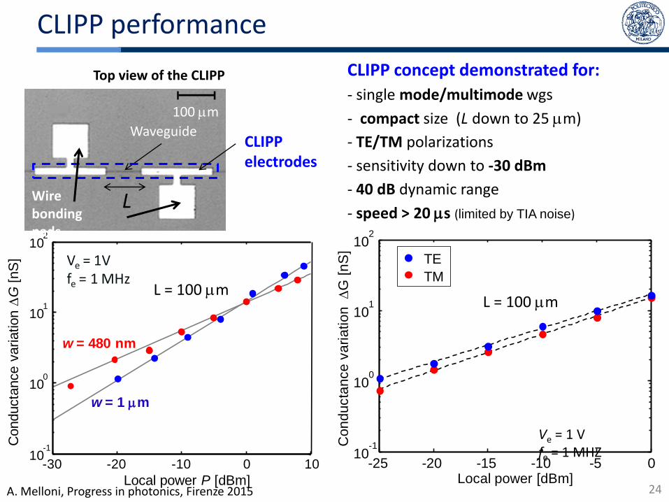
CLIPP performance
CLIPP concept demonstrated for:
- single mode/multimode wgs
- compact size (L down to 25 mm)
- TE/TM polarizations
- sensitivity down to -30 dBm
- 40 dB dynamic range
- speed > 20 ms (limited by TIA noise)
Waveguide
100 mm
-25 -20 -15 -10 -5 010
-1
100
101
102
Local power [dBm]
Con
du
cta
nce
va
ria
tio
nD
G [
nS
]
TE
TM
L
Top view of the CLIPP
-30 -20 -10 0 1010
-1
100
101
102
Conducta
nce
variation
DG
[nS
]
Local power P [dBm]
w = 480 nm
w = 1 mm
Ve = 1Vfe = 1 MHz
Ve = 1 V fe = 1 MHZ
L = 100 mm
CLIPP electrodes
Wire bonding pads
L = 100 mm
24
A. Melloni, Progress in photonics, Firenze 2015
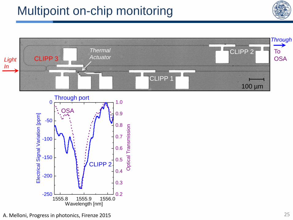
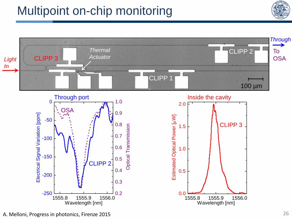
CLIPP 1
CLIPP 2 Light
In
100 µm
CLIPP 2
OSA
CLIPP 3 To
OSA
Through
Thermal
Actuator
1555.8 1555.9 1556.0-250
-200
-150
-100
-50
0
1555.8 1555.9 1556.00
50
100
150
200
250
1555.8 1555.9 1556.00.0
0.5
1.0
1.5
2.0
Estim
ate
d O
ptica
l P
ow
er
[mW
]
Ele
ctr
ica
l S
ign
al V
ariatio
n [p
pm
]
Wavelength [nm]Wavelength [nm]
InsideDrop
Ele
ctr
ica
l S
ign
al V
ariatio
n [p
pm
]
Wavelength [nm]
Through
0.2
0.3
0.4
0.5
0.6
0.7
0.8
0.9
1.0
Op
tica
l T
ran
sm
issio
n
Op
tica
l T
ran
sm
issio
n
0.0
0.1
0.2
0.3
0.4
0.5
0.6
0.7
0.8
0.9
1.0
Through port
Multipoint on-chip monitoring
25
A. Melloni, Progress in photonics, Firenze 2015
1555.8 1555.9 1556.0-250
-200
-150
-100
-50
0
1555.8 1555.9 1556.00
50
100
150
200
250
1555.8 1555.9 1556.00.0
0.5
1.0
1.5
2.0
Estim
ate
d O
ptica
l P
ow
er
[mW
]
Ele
ctr
ica
l S
ign
al V
ariatio
n [p
pm
]
Wavelength [nm]Wavelength [nm]
InsideDrop
Ele
ctr
ica
l S
ign
al V
ariatio
n [p
pm
]
Wavelength [nm]
Through
0.2
0.3
0.4
0.5
0.6
0.7
0.8
0.9
1.0
Op
tica
l T
ran
sm
issio
n
Op
tica
l T
ran
sm
issio
n
0.0
0.1
0.2
0.3
0.4
0.5
0.6
0.7
0.8
0.9
1.0
CLIPP 1
CLIPP 2 Light
In
100 µm
CLIPP 2
OSA
CLIPP 3
CLIPP 3
To
OSA
Through
Multipoint on-chip monitoring
Thermal
Actuator
Inside the cavity
1555.8 1555.9 1556.0-250
-200
-150
-100
-50
0
1555.8 1555.9 1556.00
50
100
150
200
250
1555.8 1555.9 1556.00.0
0.5
1.0
1.5
2.0
Estim
ate
d O
ptica
l P
ow
er
[mW
]
Ele
ctr
ica
l S
ign
al V
ariatio
n [p
pm
]
Wavelength [nm]Wavelength [nm]
InsideDrop
Ele
ctr
ica
l S
ign
al V
ariatio
n [p
pm
]
Wavelength [nm]
Through
0.2
0.3
0.4
0.5
0.6
0.7
0.8
0.9
1.0
Op
tica
l T
ran
sm
issio
n
Op
tica
l T
ran
sm
issio
n
0.0
0.1
0.2
0.3
0.4
0.5
0.6
0.7
0.8
0.9
1.0
Through port
26
A. Melloni, Progress in photonics, Firenze 2015
Control Layer: applications
27
A. Melloni, Progress in photonics, Firenze 2015
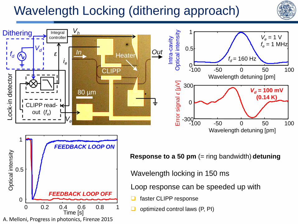
Wavelength Locking (dithering approach)
CLIPP read-
out (fe)
In Out Heater
80 µm
CLIPP
Ve
ie
Integral
controller
ε Vd
Vh
Lock-in d
ete
cto
r
Dithering
fd
Err
or
sig
na
l ε
[µV
]
Intr
a-c
avity
Op
tica
l in
ten
sity
Wavelength detuning [pm]
Wavelength detuning [pm]
Vd = 100 mV
(0.14 K)
fd = 160 Hz
-100 -50 0 50 100 0
0.5
1
-100 -50 0 50 100 -300
0
300
Response to a 50 pm (= ring bandwidth) detuning
Wavelength locking in 150 ms
Loop response can be speeded up with
faster CLIPP response
optimized control laws (P, PI) Time [s]
Op
tica
l in
ten
sity FEEDBACK LOOP ON
FEEDBACK LOOP OFF
0 0.2 0.4 0.6 0.8 1
0
0.5
1
Ve = 1 V
fe = 1 MHz

A. Melloni, Progress in photonics, Firenze 2015
V, f0
CLIPP demod. @ fe
CLIPP
demodulation
Heater
Heater
voltage Two input channels at different wavelengths
λ1 = 1549.59 nm
λ2 = λ1 + 120 pm
0 1 2 3 4 5 6 0
0.5
1
CLIPP demod. @ fe
λ2 λ1 ?
? No signal discrimination
? Heater
Heater power [mW]
Wavelength monitoring
λ2 λ1
CLIP
P s
ignal
29
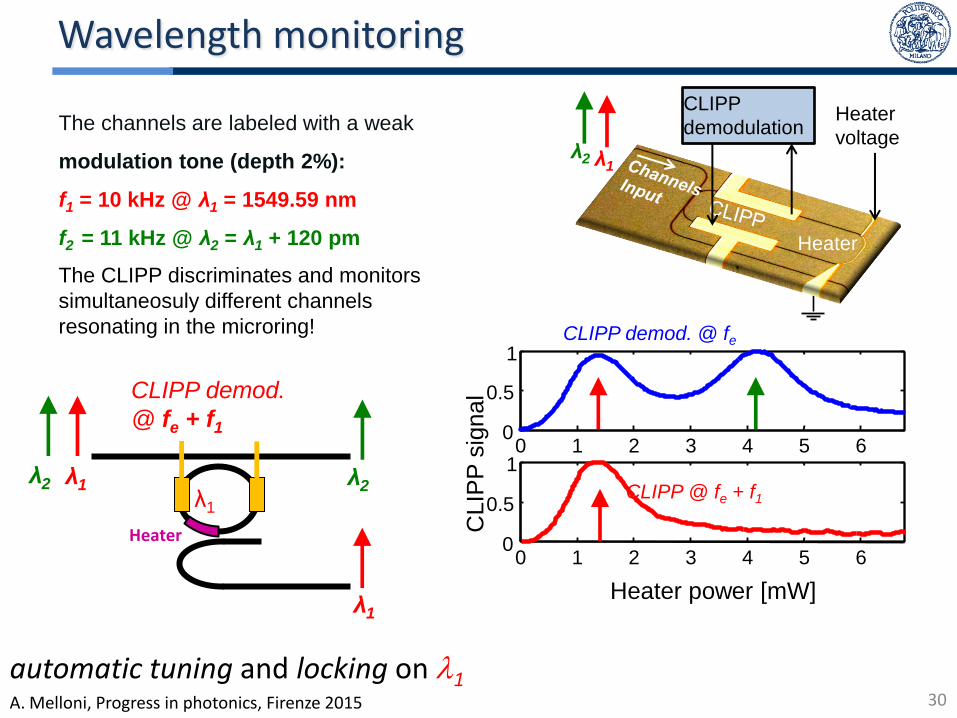
A. Melloni, Progress in photonics, Firenze 2015
CLIPP demod. @ fe
CLIPP demod.
@ fe + f1
The CLIPP discriminates and monitors
simultaneosuly different channels
resonating in the microring!
0 1 2 3 4 5 6 0
0.5
1
0 1 2 3 4 5 6 0
0.5
1
CLIPP @ fe + f1
Heater power [mW]
automatic tuning and locking on l1
λ1
Wavelength monitoring
The channels are labeled with a weak
modulation tone (depth 2%):
f1 = 10 kHz @ λ1 = 1549.59 nm
f2 = 11 kHz @ λ2 = λ1 + 120 pm V, f0
CLIPP
demodulation
Heater
Heater
voltage λ2 λ1
Heater
λ2 λ1
λ1
λ2 C
LIP
P s
ignal
30
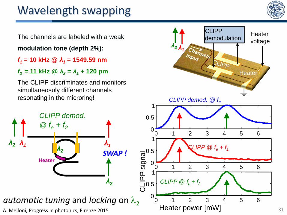
A. Melloni, Progress in photonics, Firenze 2015 Heater power [mW]
CLIP
P s
ignal
CLIPP demod. @ fe
CLIPP demod.
@ fe + f2
CLIPP @ fe + f2
0 1 2 3 4 5 6 0
0.5
1
0 1 2 3 4 5 6 0
0.5
1 0 1 2 3 4 5 6
0
0.5
1
CLIPP @ fe + f1
automatic tuning and locking on l2
SWAP !
Wavelength swapping
The CLIPP discriminates and monitors
simultaneosuly different channels
resonating in the microring!
The channels are labeled with a weak
modulation tone (depth 2%):
f1 = 10 kHz @ λ1 = 1549.59 nm
f2 = 11 kHz @ λ2 = λ1 + 120 pm V, f0
CLIPP
demodulation
Heater
Heater
voltage λ2 λ1
Heater
λ2 λ1
λ2
λ1 λ2
31

A. Melloni, Progress in photonics, Firenze 2015 32
• generate the CLIPPs driving signal Ve (fast DAC);
• provide the I/Q clock signals to the lock-ins in the ASIC;
• drive the heaters integrated onto the photonic chip (slow DACs);
• FPGA-based digital processing ;
• control of up to 16 independent feedback control-loops;
Multichannel feedback control
Motherboard
Motherboard ASIC
Photonic chip
ASIC
Photonic chip
Motherboard:
32
A. Melloni, Progress in photonics, Firenze 2015 33
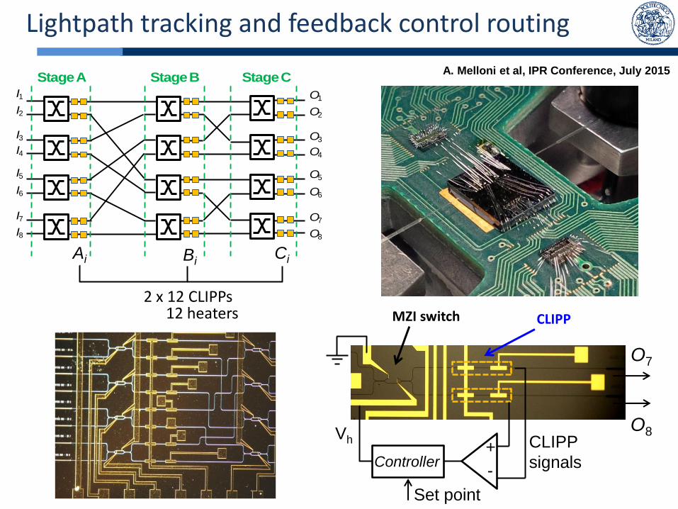
2 x 12 CLIPPs
Ai Bi Ci
Stage A Stage B Stage CI1
I2
I3
I4
I5
I6
I7
I8
O1
O2
O3
O4
O5
O6
O7
O8
CLIPP MZI switch
PHOTONI C
CHI P
O7
O8 Vh CLIPP
signals +
- Controller
Set point
Lightpath tracking and feedback control routing
A. Melloni et al, IPR Conference, July 2015
12 heaters
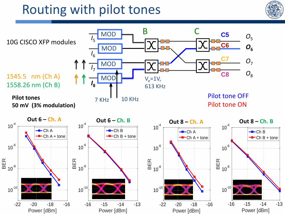
A. Melloni, Progress in photonics, Firenze 2015 -22 -20 -18 -16
10-10
10-8
10-6
10-4
Power [dBm]
BE
R
Ch A
Ch A + tone
-16 -15 -14 -13
10-10
10-8
10-6
10-4
Power [dBm]
BE
R
Ch B
Ch B + tone
-22 -20 -18 -16
10-10
10-8
10-6
10-4
Power [dBm]
BE
R
Ch A
Ch A + tone
-16 -15 -14 -13
10-10
10-8
10-6
10-4
Power [dBm]
BE
R
Ch B
Ch B + tone
Pilot tone OFF Pilot tone ON
Out 8 – Ch. A Out 8 – Ch. B Out 6 – Ch. A Out 6 – Ch. B
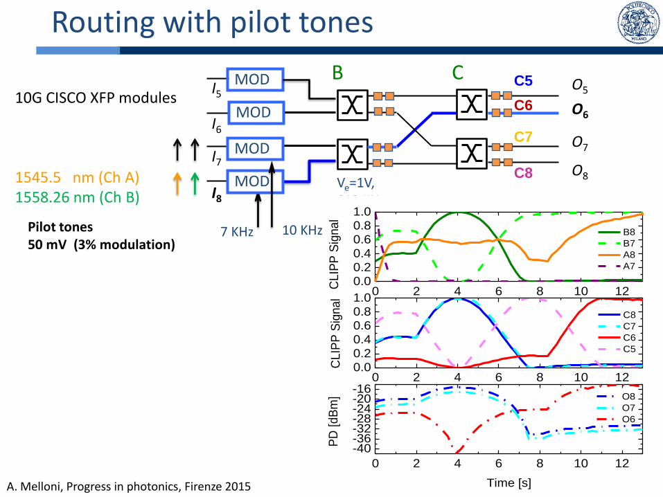
Routing with pilot tones
MOD
MOD
MOD
MOD
Pilot tones 50 mV (3% modulation)
B C
Ve=1V, 613 KHz
10 KHz 7 KHz
10G CISCO XFP modules 1545.5 nm (Ch A) 1558.26 nm (Ch B)
C5
C6
C7
C8
I8
I7
I6
I5
O8
O7
O6
O5
0 2 4 6 8 10 120.00.20.40.60.81.0
0 2 4 6 8 10 120.00.20.40.60.81.0
0 2 4 6 8 10 12
-40-36-32-28-24-20-16
C8
C7
C6
C5
CLIP
P S
ignal
B8
B7
A8
A7
CLIP
P S
ignal
O8
O7
O6
PD
[dB
m]
Time [s]
A. Melloni, Progress in photonics, Firenze 2015 -22 -20 -18 -16
10-10
10-8
10-6
10-4
Power [dBm]
BE
R
Ch A
Ch A + tone
-16 -15 -14 -13
10-10
10-8
10-6
10-4
Power [dBm]
BE
R
Ch B
Ch B + tone
-22 -20 -18 -16
10-10
10-8
10-6
10-4
Power [dBm]
BE
R
Ch A
Ch A + tone
-16 -15 -14 -13
10-10
10-8
10-6
10-4
Power [dBm]
BE
R
Ch B
Ch B + tone
Pilot tone OFF Pilot tone ON
Out 8 – Ch. A Out 8 – Ch. B Out 6 – Ch. A Out 6 – Ch. B
Routing with pilot tones
MOD
MOD
MOD
MOD
Pilot tones 50 mV (3% modulation)
B C
Ve=1V, 613 KHz
10 KHz 7 KHz
10G CISCO XFP modules 1545.5 nm (Ch A) 1558.26 nm (Ch B)
C5
C6
C7
C8
I8
I7
I6
I5
O8
O7
O6
O5
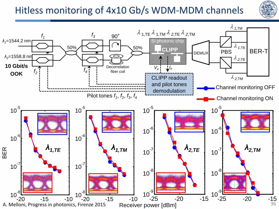
A. Melloni, Progress in photonics, Firenze 2015
λ1=1544.2 nm
λ2=1558.8 nm
Hitless monitoring of 4x10 Gb/s WDM-MDM channels
Receiver power [dBm]
BE
R
-20 -15 -1010
-8
10-7
10-6
10-5
-20 -15 -1010
-8
10-7
10-6
10-5
-25 -20 -1510
-9
10-8
10-7
10-6
10-5
-25 -20 -1510
-9
10-8
10-7
10-6
10-5
λ1,TE λ1,TM λ2,TE λ2,TM
50% 50% CLIPP
ie
CLIPP readout
and pilot tones
demodulation
90°
10 Gbit/s
OOK
l 1,TE l 1,TM l 2,TE l 2,TM
Pilot tones f1, f2, f3, f4
PBS BER-T
l 2,TM
l 1,TM
l 2,TE
l 1,TE
DEMUX
f1
f2
f3
f4
Channel monitoring OFF
Channel monitoring ON
Si photonic chip
Ve Decorrelation
fiber coil
36
A. Melloni, Progress in photonics, Firenze 2015
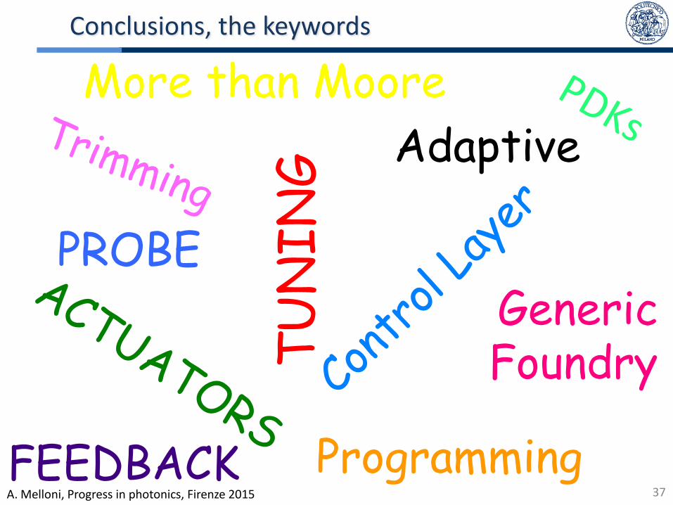
TU
NIN
G Adaptive
PROBE
Programming FEEDBACK
Conclusions, the keywords
Generic Foundry
More than Moore
37
A. Melloni, Progress in photonics, Firenze 2015
Eu Project – ICT/FET (2013-2016) Breaking the barriers of Optical Integration www.bboi.eu
Acknowledgments
We acknowledge financial support from:
Italian National Research Project SAPPHIRE
Shared Access Platform to PHotonic Integrated Resources
Prof. Marc Sorel & Dr. Michael J. Strain
James Watt Nanofabrication Center at University of Glasgow
for support in the fabrication of the silicon photonic devices
We are grateful to:


